Semiconductor Memory Device
KAWASUMI; Atsushi ; et al.
U.S. patent application number 16/558822 was filed with the patent office on 2020-09-17 for semiconductor memory device. The applicant listed for this patent is TOSHIBA MEMORY CORPORATION. Invention is credited to Tsuneo INABA, Atsushi KAWASUMI.
| Application Number | 20200295087 16/558822 |
| Document ID | / |
| Family ID | 1000004337345 |
| Filed Date | 2020-09-17 |


View All Diagrams
| United States Patent Application | 20200295087 |
| Kind Code | A1 |
| KAWASUMI; Atsushi ; et al. | September 17, 2020 |
SEMICONDUCTOR MEMORY DEVICE
Abstract
A semiconductor memory device includes a first wiring extending in a first direction, a second wiring above the first wiring and extending in a second direction, first and second memory cells electrically connected in parallel between the first and second wirings and each including a phase change material, a first insulating film on a side portion of the first cell facing the second cell in the second direction, a third wiring above the second wiring and extending in the second direction, a fourth wiring above the third wiring and extending in the first direction, third and fourth memory cells electrically connected between the third and fourth wirings in parallel and each including a phase change material, and a second insulating film on a side of the third cell facing the fourth cell in the second direction. The first film has a higher thermal insulation capacity than the second film.
| Inventors: | KAWASUMI; Atsushi; (Fujisawa Kanagawa, JP) ; INABA; Tsuneo; (Kamakura Kanagawa, JP) | ||||||||||
| Applicant: |
|
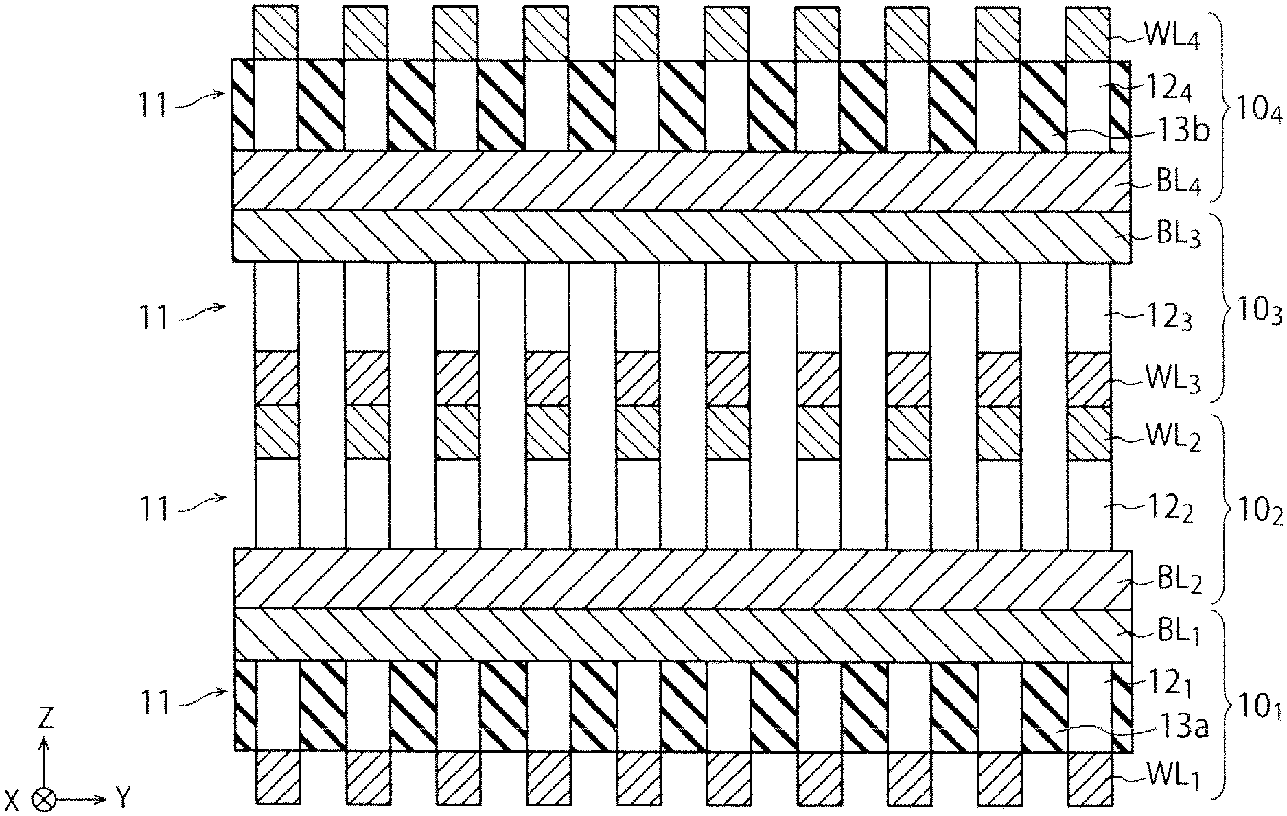
||||||||||
|---|---|---|---|---|---|---|---|---|---|---|---|
| Family ID: | 1000004337345 | ||||||||||
| Appl. No.: | 16/558822 | ||||||||||
| Filed: | September 3, 2019 |
| Current U.S. Class: | 1/1 |
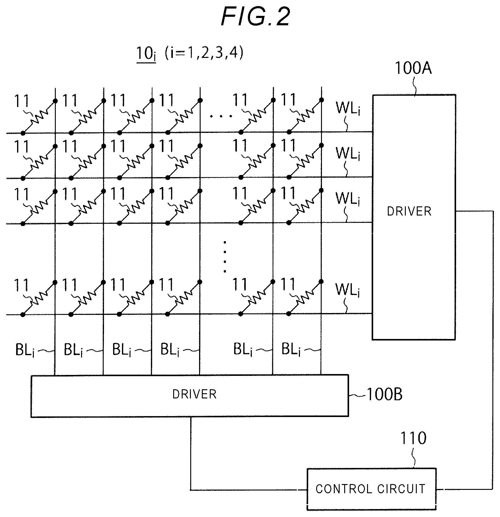
| Current CPC Class: | H01L 45/06 20130101; H01L 27/2481 20130101; H01L 45/141 20130101; H01L 45/1293 20130101 |
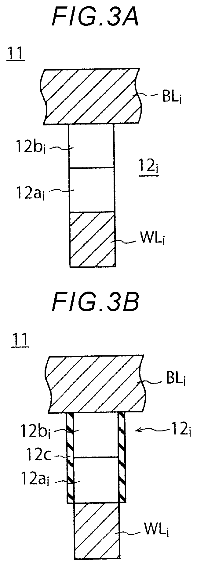
| International Class: | H01L 27/24 20060101 H01L027/24; H01L 45/00 20060101 H01L045/00 |
Foreign Application Data
| Date | Code | Application Number |
|---|---|---|
| Mar 15, 2019 | JP | 2019-048620 |
Claims
1. A semiconductor memory device comprising: a first wiring extending in a first direction; a second wiring above the first wiring and extending in a second direction intersecting the first direction; first and second memory cells electrically connected in parallel between the first and second wirings and each including a phase change material; a first insulating film on a side portion of the first memory cell that faces the second memory cell in the second direction; a third wiring above the second wiring and extending in the second direction; a fourth wiring above the third wiring and extending in the first direction; third and fourth memory cells electrically connected between the third and fourth wirings in parallel and each including a phase change material; and a second insulating film on a side portion of the third memory cell that faces the fourth memory cell in the second direction, wherein the first insulating film has a higher thermal insulation capacity than the second insulating film.
2. The semiconductor memory device according to claim 1, further comprising: a fifth wiring above the fourth wiring and extending in the first direction; a sixth wiring above the fifth wiring and extending in the second direction; fifth and sixth memory cells electrically connected in parallel between the fifth and sixth wirings and each including a phase change material; and a third insulating film on a side portion of the fifth memory cell that faces the sixth memory cell in the second direction, wherein the first insulating film has a higher thermal insulation capacity than the third insulating film.
3. The semiconductor memory device according to claim 2, wherein the second and third insulating films have substantially the same thermal insulation capacity.
4. The semiconductor memory device according to claim 1, wherein the second and third wirings are in contact with each other.
5. The semiconductor memory device according to claim 2, further comprising: a seventh wiring above the sixth wiring and extending in the second direction; an eighth wiring above the seventh wiring and extending in the first direction; seventh and eighth memory cells electrically connected in parallel between the seventh and eighth wirings and each including a phase change material; and a fourth insulating film on a side portion of the seventh memory cell that faces the eighth memory cell in the second direction, wherein the fourth insulating film has a higher thermal insulation capacity than the second and third insulating films.
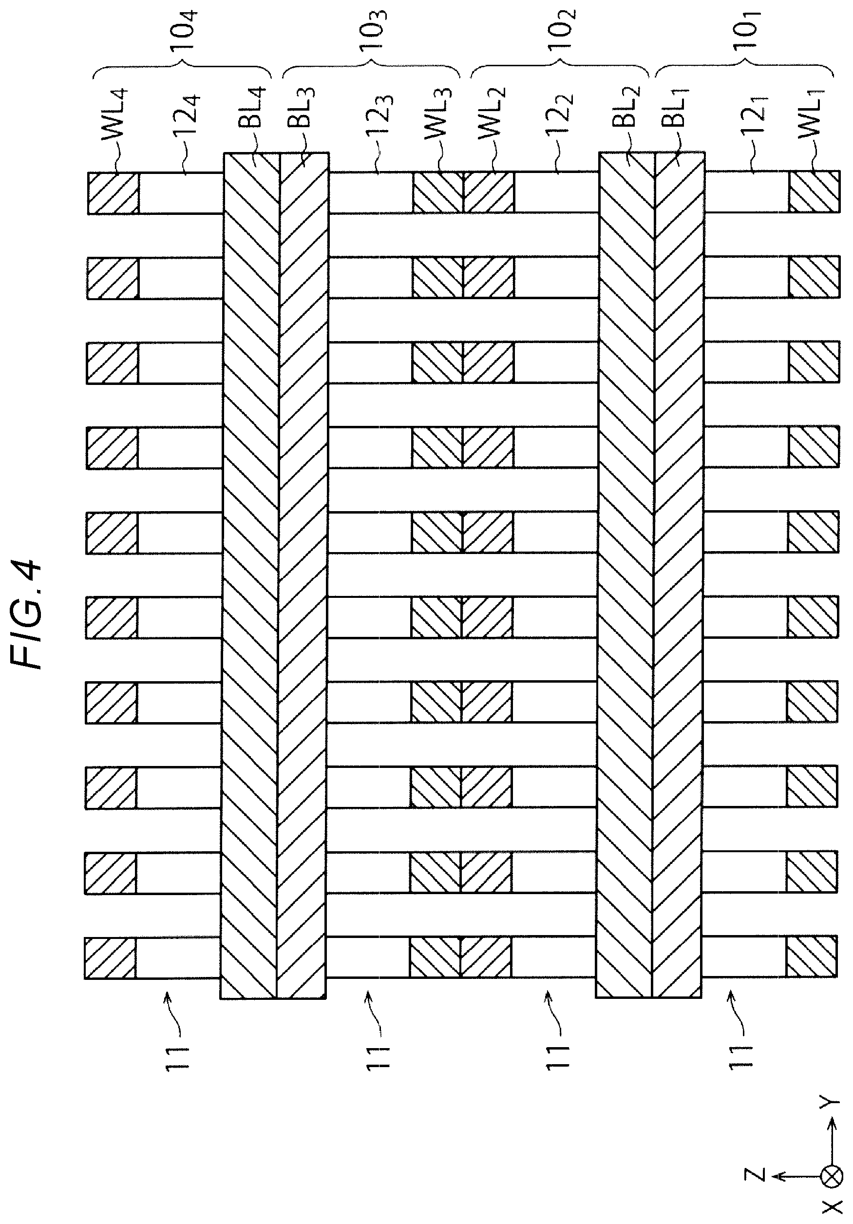
6. The semiconductor memory device according to claim 5, wherein the first wiring, the second wiring, the first and second memory cells, and the first insulating film are included in a lowermost layer of the semiconductor memory device, and the seventh wiring, the eighth wiring, the seventh and eighth memory cells, and the fourth insulating film are included in an uppermost layer of the semiconductor device.
7. The semiconductor memory device according to claim 1, wherein the first insulation film covers an entire side surface of the first memory cell.
8. The semiconductor memory device according to claim 1, wherein the first insulating film contains one of porous silicon, silicon nitride, and carbon.
9. The semiconductor memory device according claim 1, wherein each memory cell includes a storage layer containing the phase change material and a switching element to select the memory cell.
10. The semiconductor memory device according to claim 1, wherein the phrase change material is chalcogenide.
11. A semiconductor memory device comprising: a first wiring extending in a first direction; a second wiring above the first wiring and extending in a second direction intersecting the first direction; a first memory cell electrically connected between the first and second wirings and including a phase change material; a third wiring above the second wiring and extending in the second direction; a fourth wiring above the third wiring and extending in the first direction; and a second memory cell electrically connected between the third and fourth wirings and including a phase change material, wherein the first memory cell has a shorter length in the second direction than the second memory cell.
12. The semiconductor memory device according to claim 11, further comprising: a fifth wiring above the fourth wiring and extending in the first direction; a sixth wiring above the fifth wiring and extending in the second direction; a third memory cell electrically connected between the fifth and sixth wirings and including a phase change material, wherein the first memory cell has a shorter length in the second direction than the third memory cell.
13. The semiconductor memory device according to claim 12, wherein the second and third memory cells have substantially the same length in the second direction.
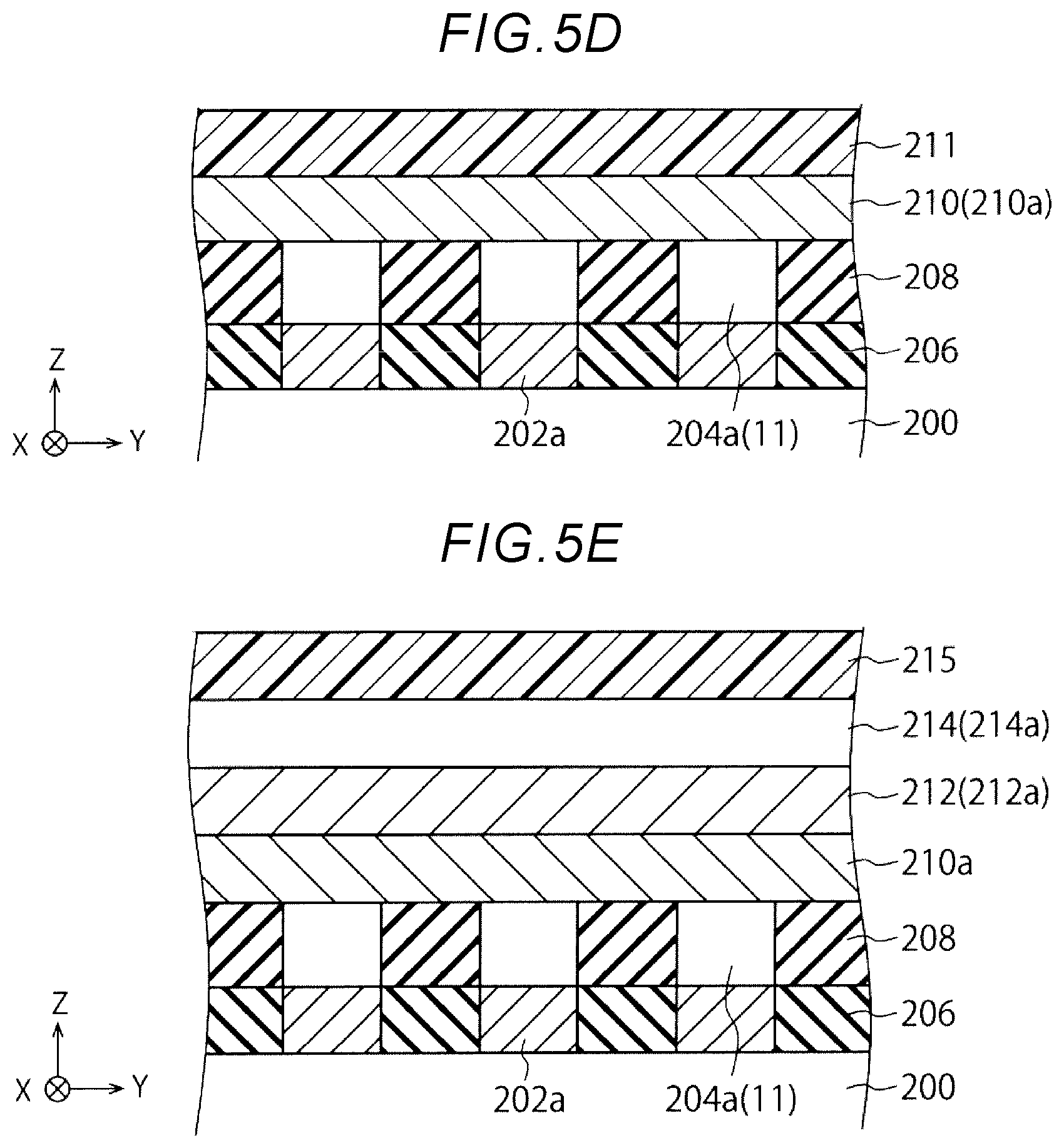
14. The semiconductor memory device according to claim 12, further comprising: a seventh wiring above the sixth wiring and extending in the second direction; an eighth wiring above the seventh wiring and extending in the first direction; and a fourth memory cell electrically connected between the seventh and eighth wirings and including a phase change material, wherein the fourth memory cell has a shorter length in the second direction than the second and third memory cells.
15. The semiconductor memory device according to claim 14, wherein the first wiring, the second wiring, the first memory cell, and the first insulating film are included in a lowermost layer of the semiconductor memory device, and the seventh wiring, the eighth wiring, and the fourth memory cell are included in an uppermost layer of the semiconductor device.
16. The semiconductor memory device according claim 11, wherein each memory cell includes a storage layer containing the phase change material and a switching element to select the memory cell.
17. The semiconductor memory device according to claim 11, wherein the phrase change material is chalcogenide.
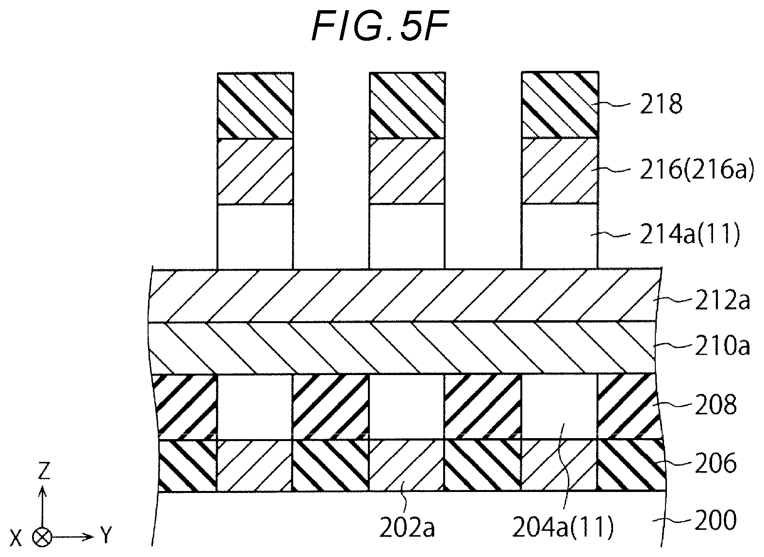
18. A semiconductor memory device comprising: a first wiring extending in a first direction; a second wiring above the first wiring and extending in a second direction intersecting the first direction; a first memory cell electrically connected between the first and second wirings and including a phase change material; a third wiring above the second wiring and extending in the second direction; a fourth wiring above the third wiring and extending in the first direction; and a second memory cell electrically connected between the third and fourth wirings and including a phase change material, wherein the first wiring has a longer length in the second direction than the fourth wiring.
19. The semiconductor memory device according to claim 18, further comprising: a fifth wiring above the fourth wiring and extending in the first direction; a sixth wiring above the fifth wiring and extending in the second direction; and a third memory cell electrically connected between the fifth and sixth wirings and including a phase change material, wherein the first wiring has a longer length in the second direction than the fifth wiring.
20. The semiconductor memory device according to claim 19, further comprising: a seventh wiring above the sixth wiring and extending in the second direction; an eighth wiring above the seventh wiring and extending in the first direction; a fourth memory cell electrically connected between the seventh and eighth wirings and including a phase change material, wherein the eighth wiring has a longer length in the second direction than the fourth and fifth wirings.
Description
CROSS-REFERENCE TO RELATED APPLICATION(S)
[0001] This application is based upon and claims the benefit of priority from Japanese Patent Application No. 2019-048620, filed Mar. 15, 2019, the entire contents of which are incorporated herein by reference.
FIELD
[0002] Embodiments described herein relate generally to a semiconductor memory device including a phase change memory element.
BACKGROUND
[0003] A known cross-point type semiconductor memory includes a phase change memory (PCM) element that is electrically connected between wirings that extend in intersecting directions and has a storage layer formed of a phase change material.
[0004] When the semiconductor memory is formed across multiple layers to achieve high integration, reliability of the operation of PCM elements in the lowermost layer and uppermost layer may be decreased.
DESCRIPTION OF THE DRAWINGS
[0005] FIG. 1 is a cross-sectional view of a semiconductor memory device according to a first embodiment.
[0006] FIG. 2 is a circuit diagram of a semiconductor memory device according to the first embodiment.
[0007] FIG. 3A is a cross-sectional view of a memory cell according to the first embodiment.
[0008] FIG. 3B is a cross-sectional view of a modification of the memory cell according to the first embodiment.
[0009] FIG. 4 is a cross-sectional view of a semiconductor memory device according to a comparative example.
[0010] FIG. 5A to FIG. 5F are cross-sectional views for explaining a method for manufacturing the semiconductor memory device according to the first embodiment.
[0011] FIG. 6 is a cross-sectional view of a semiconductor memory device according to a second embodiment.
[0012] FIG. 7A is a cross-sectional view for explaining a method for manufacturing the semiconductor memory device according to the second embodiment.
[0013] FIG. 7B is a cross-sectional view of a modification of the semiconductor memory device according to the second embodiment.
[0014] FIG. 8 is a cross-sectional view of a semiconductor memory device according to a third embodiment.
[0015] FIG. 9 is a cross-sectional view of a semiconductor memory device according to a fourth embodiment.
DETAILED DESCRIPTION
[0016] In general, according to one embodiment, a semiconductor memory device includes a first wiring extending in a first direction, a second wiring above the first wiring and extending in a second direction intersecting the first direction, first and second memory cells electrically connected in parallel between the first and second wirings and each including a phase change material, a first insulating film on a side portion of the first memory cell that faces the second memory cell in the second direction, a third wiring above the second wiring and extending in the second direction, a fourth wiring above the third wiring and extending in the first direction, third and fourth memory cells electrically connected between the third and fourth wirings in parallel and each including a phase change material, a second insulating film on a side portion of the third memory cell that faces the fourth memory cell in the second direction. The first insulating film has a higher thermal insulation capacity than the second insulating film.
First Embodiment
[0017] A cross section of a semiconductor memory device according to a first embodiment is shown in FIG. 1. The semiconductor memory device according to the first embodiment includes first to fourth semiconductor memories 10.sub.1 to 10.sub.4 that are formed across multiple layers. Each semiconductor memory 10.sub.i (i=1, . . . , 4) is a cross-point type semiconductor memory, and includes a plurality of phase change memory elements 11 (hereinafter, also referred to as memory cells). Further, each semiconductor memory 10.sub.i (i=1, . . . , 4) includes a plurality of word lines WL.sub.i (e.g., ten word lines) arranged in parallel, a plurality of bit lines BL.sub.i extending along a direction intersecting these word lines WL.sub.i, and a storage unit 12i disposed in an intersection region between the word line WL.sub.i and the bit line BL.sub.i. The plurality of bit lines BL.sub.i (i=1, . . . , 4) are also arranged in parallel in the same manner as the word line WL.sub.i. That is, in each semiconductor memory 10.sub.i (i=1, . . . , 4), each memory cell 11 includes a corresponding word line WL.sub.i, a corresponding bit line BL.sub.i, and the storage unit 12i provided in the intersection region between the word line WL.sub.i and the bit line BL.sub.i. Therefore, in FIG. 2, each semiconductor memory 10.sub.i (i=1, . . . , 4) includes 10 memory cells 11.
[0018] Each word line WL.sub.1 of the first semiconductor memory 10.sub.1 extends along x direction as shown in FIG. 1. The storage unit 12.sub.1 is disposed above these word lines WL.sub.1. The bit line BL.sub.1 is disposed above the storage unit 12.sub.1. The plurality of bit lines BL.sub.1 separately extend along y direction intersecting the x direction, and FIG. 2 only shows one bit line BL.sub.1. An interlayer insulating film (e.g., silicon oxide) (not shown) is disposed between the plurality of word lines WL.sub.1. An insulating film 13a is formed of a material having a heat insulating property higher than that of a material of the above interlayer insulating film, and is disposed between the plurality of storage units 12.sub.1. In addition, an interlayer insulating film (not shown) is disposed between the plurality of bit lines BL.sub.1. This interlayer insulating film is formed of a material having a heat insulating property lower than that of the material of the insulating film 13a.
[0019] The bit lines BL.sub.2 of the second semiconductor memory 10.sub.2 are arranged along the y direction above the bit lines BL.sub.1 of the first semiconductor memory 10.sub.1. The bit lines BL.sub.2 are arranged in parallel in the same manner as the plurality of bit lines BL.sub.1. The storage unit 12.sub.2 is disposed above each bit line BL.sub.2 of the second semiconductor memory 10.sub.2. The word lines WL.sub.2 of the second semiconductor memory 10.sub.2 are disposed above each storage unit 12.sub.2. The word lines WL.sub.2 are arranged along the x direction in the same manner as the plurality of word lines WL.sub.1. An interlayer insulating film (not shown) is disposed between the plurality of bit lines BL.sub.2, between the plurality of storage units 12.sub.2, and between the plurality of word lines WL.sub.2.
[0020] The word lines WL.sub.3 of the third semiconductor memory 10.sub.3 are disposed above the word lines WL.sub.2 of the second semiconductor memory 10.sub.2. The word lines WL.sub.3 each extend along the x direction in the same manner as the word lines WL.sub.2 of the second semiconductor memory 10.sub.2. Further, the storage units 12.sub.3 of the third semiconductor memory 10.sub.3 are disposed above these word lines WL.sub.3. The bit lines BL.sub.3 of the third semiconductor memory 10.sub.3 are disposed above the storage units 12.sub.3. The bit lines BL.sub.3 each extend along the y direction. An interlayer insulating film (not shown) is disposed between the plurality of word lines WL.sub.3, between the plurality of storage units 12.sub.3, and between the plurality of bit lines BL.sub.3.
[0021] The bit lines BL.sub.4 of the fourth semiconductor memory 10.sub.4 are disposed above the bit lines BL.sub.3 of the third semiconductor memory 10.sub.3. The bit lines BL.sub.4 each extend along the y direction in the same manner as the plurality of bit lines BL.sub.1. The storage unit 12.sub.4 is disposed above each bit line BL.sub.4 of the fourth semiconductor memory 10.sub.4. The word lines WL.sub.4 of the fourth semiconductor memory 10.sub.4 are disposed above the storage units 12.sub.4. The word lines WL.sub.4 each extend along the x direction in the same manner as the plurality of word lines WL.sub.1. An interlayer insulating film (not shown) is disposed between the plurality of bit lines BL.sub.4. An insulating film 13b is formed of a material having a higher heat insulating property than that of a material of the interlayer insulating film, and is disposed between the plurality of storage units 12.sub.4. Further, an interlayer insulating film (not shown) is disposed between the plurality of word lines WL.sub.4. The interlayer insulating film is formed of a material having a heat insulating property lower than that of the material of the insulating film 13b.
[0022] In this manner, in the semiconductor memory device according to the first embodiment and other embodiments described below, the first to fourth semiconductor memories 10.sub.1 to 10.sub.4 are stacked along z direction intersecting the x direction and the y direction.
[0023] Further, as shown in FIG. 2, in each semiconductor memory 10.sub.i (i=1, 2, 3, 4), the plurality of word lines WL.sub.i are connected to a driver 100A, and the plurality of bit lines BL.sub.i are connected to a driver 100B. The driver 100A and the driver 100B are connected to a control circuit 110. The driver 100A selects one word line among the plurality of word lines WL.sub.i based on an instruction from the control circuit 110, and applies a write voltage to the selected word line. The driver 100B selects one bit line among the plurality of bit lines BL.sub.i based on an instruction from the control circuit 110, and applies a write voltage to the selected bit line. The memory cell 11 is disposed in the intersection region between each word line WL.sub.i and each bit line BL.sub.i. One end of the memory cell 11 is connected to the corresponding word line WL.sub.i, and the other end thereof is connected to the corresponding bit line BL.sub.i. The driver 100A and the driver 100B may be provided in each semiconductor memory 10.sub.i (i=1, 2, 3, 4), or may be provided commonly in all of the semiconductor memories 10.sub.1 to 10.sub.4.
[0024] In the semiconductor memory device according to the first embodiment and any one of the second to fourth embodiments described below, the memory cell 11 used for each of the semiconductor memories 10.sub.1 to 10.sub.4 has a structure shown in FIG. 3A. The memory cell 11 includes the storage unit 12i between the corresponding word line WL.sub.i (i=1, 2, 3, 4) and the corresponding bit line BL.sub.i. The storage unit 12i has a structure in which a switching element 12a.sub.i and a storage layer 12b.sub.i are stacked. In the example shown in FIG. 3A, while the switching element 12a.sub.i is provided on a word line WL.sub.i side, and the storage layer 12b.sub.i is provided on a bit line BL.sub.i side, the switching element 12a.sub.i may be provided on the bit line BL.sub.i side, and the storage layer 12b.sub.i may be provided on the word line WL.sub.i side.
[0025] When the memory cell 11 shown in FIG. 3A is selected, the switching element 12a.sub.i has a function of preventing a write current from flowing to another memory cell 11 that is not selected through the word line WL.sub.i or the bit line BL.sub.i. That is, the switching element 12a.sub.i is used to select the memory cell. Further, for example, AsGeTeSiN or SiTe is used as the switching element 12a.sub.i.
[0026] The storage layer 12b.sub.i contains a phase change material that changes the phase between a crystalline phase and an amorphous phase. The phase change material includes, for example, a chalcogenide alloy (e.g., GeSbTe alloy). That is, the chalcogenide alloy includes chalcogenide and, for another example, an AsSbTe alloy, a TaSbTe alloy, a NbSbTe alloy, VSbTe alloy, a NbSbSe alloy, a VSbSe alloy, a WSbTe alloy, a WSbTe alloy, a MoSbTe alloy, a CrSbTe alloy, a WSbSe alloy, a MoSbSe alloy, a CrSbSe alloy or a SnSbTe alloy is used. After being heated and dissolved, the phase change material becomes the crystalline phase when subjected to slow cooling (i.e., gradual cooling) and has a low resistance value, and becomes the amorphous phase when subjected to rapid cooling and has a high resistance value. Therefore, a voltage is applied between the corresponding word line WL.sub.i and the corresponding bit line BL.sub.i of the memory cell to heat the storage unit 12i, and thereafter, if a drop speed of the voltage is increased, the phase change material of the storage unit 12i is rapidly cooled to be in the amorphous phase and to be in the high resistance state. In addition, after being heated, if the drop speed of the voltage is reduced, the phase change material of the storage unit 12i is slowly cooled to be in the crystalline state and to be in the low resistance state.
[0027] The insulating layers 13a and 13b formed of a material having a heat insulating property higher than that of a material of the interlayer insulating film contains, for example, any one of porous silicon, silicon nitride, and carbon.
[0028] For example, the word line WL.sub.i (i=1, 2, 3, 4) and the bit line BL.sub.i are formed of tungsten (W). Alternatively, the word line WL.sub.i (i=1, 2, 3, 4) and the bit line BL.sub.i may be formed of stacked structure of tungsten (W), ruthenium (Ru), and molybdenum (Mo).
[0029] In the semiconductor memory device according to the first embodiment configured as described above, at least side surfaces of the storage layer 12b.sub.1 and the storage layer 12b.sub.4 of the memory cell 11 of the lowermost layer semiconductor memory 10.sub.1 and the memory cell 11 of the uppermost layer semiconductor memory 10.sub.4 are respectively covered with the insulating film 13a and the insulating film 13b having a high heat insulating property. Therefore, when a write voltage same as that of the memory cell of another layer semiconductor memory is applied to the memory cell 11 of the lowermost layer semiconductor memory 10.sub.1 or the uppermost layer semiconductor memory 10.sub.4, the heat escaping from the storage layer to the interlayer insulating film is reduced. That is, the memory cell 11 of the lowermost layer semiconductor memory 10.sub.1 and the memory cell 11 of the uppermost layer semiconductor memory 10.sub.4 can perform a reset operation using a reduced reset current. Therefore, according to the first embodiment, it is possible to provide a semiconductor memory device capable of preventing a decrease in reliability of a reset operation even during high integration. Therefore, the number of memory cells to be written by the driver can be increased, and the number of memory cells of the semiconductor memory provided in the same layer can be increased.
[0030] (Modification)
[0031] A modification of the memory cell 11 is shown in FIG. 3B. In the semiconductor memory device according to the first embodiment and any one of the second to fourth embodiments described below, the memory cell 11 of the modification is used as the memory cell of the semiconductor memories 10.sub.1 to 10.sub.4. In the memory cell 11 shown in FIG. 3B, a heat insulating layer 12c is provided to cover at least a side surface of the storage layer 12b.sub.i (i=1, 2, 3, 4) in the memory cell shown in FIG. 3A. The heat insulating layer 12c is formed of a material having a heat insulating property higher than that of the material of the interlayer insulating film of the middle layer semiconductor memories 10.sub.2 and 10.sub.3. An interlayer insulating film having a heat insulating property lower than that of the material of the heat insulating layer 12c is provided between the memory cells 11. The heat insulating layer 12c may be provided to cover side surfaces of the switching elements 12a.sub.1 and 12a.sub.4.
[0032] When the memory cell 11 shown in FIG. 3B is used as the memory cells 11 of the middle layer semiconductor memories 10.sub.2 and 10.sub.3, the insulating films 13a and 13b formed of a material having a high heat insulating property are provided on the periphery of the memory cell 11 (i.e., the side portion of the memory cell 11) between the memory cells of the lowermost layer and uppermost layer semiconductor memories 10.sub.1 and 10.sub.4 in the same manner as the first embodiment shown in FIG. 1.
[0033] In addition, the memory cell 11 shown in FIG. 3B may also be used as the memory cells 11 of the lowermost layer and uppermost layer semiconductor memories 10.sub.1 and 10.sub.4. In this case, the memory cell 11 shown in FIG. 3B is not provided between the memory cells 11 of the middle layer semiconductor memories 10.sub.2 and 10.sub.3, and the interlayer insulating film having a low heat insulating property is provided in the same manner as the first embodiment. It is also possible to provide the memory cell 11 shown in FIG. 3B between the memory cells 11 of the semiconductor memories 10.sub.2 and 10.sub.3. In this case, a thickness of the heat insulating layer 12c in the y direction in the memory cell 11 of the semiconductor memories 10.sub.1 and 10.sub.4 is thicker than a thickness of the heat insulating layer 12c in the y direction in the memory cell 11 of the semiconductor memories 10.sub.2 and 10.sub.3.
[0034] In the present modification, it is also possible to provide a semiconductor memory device capable of preventing a decrease in reliability of a reset operation even during high integration.
Comparative Example
[0035] Next, a semiconductor memory device according to a comparative example is shown in FIG. 4. The semiconductor memory device according to the comparative example has a configuration in which a material of the interlayer insulating film disposed on the periphery of the middle layer memory cell 11 (i.e., an insulating film having a heat insulating property lower than that of the material of the insulating films 13a and 13b) is disposed in the lowermost layer and uppermost layer semiconductor memories 10.sub.1 and 10.sub.4, instead of the insulating films 13a and 13b according to the first embodiment shown in FIG. 1.
[0036] In the semiconductor memory device according to the comparative example, the bit line BL.sub.1 of the first semiconductor memory 10.sub.1 and the bit line BL.sub.2 of the second semiconductor memory 10.sub.2 are disposed overlapping each other. The word line WL.sub.2 of the second semiconductor memory 10.sub.2 and the word line WL.sub.3 of the third semiconductor memory 10.sub.3 are disposed overlapping each other. The bit line BL.sub.3 of the third semiconductor memory 10.sub.3 and the bit line BL.sub.4 of the fourth semiconductor memory 10.sub.4 are disposed overlapping each other. However, a lowermost layer wiring of the lowermost layer (i.e., word line WL.sub.1 in FIG. 4) and an uppermost layer wiring of the uppermost layer (i.e., word line WL.sub.4 in FIG. 4) of the lowermost layer of the semiconductor memories do not overlap with any other wiring (i.e., are not adjacent to any other wiring), as compared with other overlapped wirings, for example, the bit line BL.sub.1 of the first semiconductor memory 10.sub.1 and the bit line BL.sub.2 of the second semiconductor memory 10.sub.2. Thus, the thickness of each of the lowermost layer wiring and the uppermost layer wiring of the uppermost layer is thinner. Therefore, when a write voltage is applied to the corresponding memory cell 11, the wiring resistance is high.
[0037] Therefore, even when the same write voltage is applied to the corresponding bit line and the corresponding word line in a reset operation of the memory cells 11 of the lowermost layer semiconductor memory 10.sub.1 and the uppermost layer semiconductor memory 10.sub.4, that is, an operation is performed to change the state of the memory cells from the low resistance state (i.e., the crystalline state) to the high resistance state (i.e., the amorphous state), as compared with the operation the memory cells of other layer semiconductor memories 10.sub.2 and 10.sub.3, the write current supplied to the corresponding storage unit 12i is smaller, and the reset operation is not normally performed. Therefore, the number of the memory cells to be written by a writing circuit cannot be increased, and the number of the memory cells of the semiconductor memory provided in the same layer is limited.
[0038] (Method for Manufacturing Semiconductor Memory Device According to First Embodiment)
[0039] Next, a method for manufacturing the semiconductor memory device according to the first embodiment will be described with reference to FIG. 5A to FIG. 5F.
[0040] As shown in FIG. 5A, a wiring material layer 202 is formed above a semiconductor layer 200, and a memory cell material layer 204 is formed above the wiring material layer 202. Thereafter, a line-and-space shaped mask 205 that extends along the x direction is formed above the memory cell material layer 204. The mask 205 is formed of, for example, a photosensitive resin, and is formed by using a lithography technique.
[0041] Next, for example, reactive ion etching (RIE) is performed on the memory cell material layer 204 by using the mask 205 to form a line-shaped pattern 204a that extends along the x direction. Thereafter, RIE is performed on the wiring material layer 202 by using the mask 205 to form a line-shaped wiring 202a that extends along the x direction (FIG. 5B). The wiring 202a is, for example, the word line WL.sub.1 shown in FIG. 1.
[0042] Subsequently, as shown in FIG. 5C, the mask 205 is removed, then an insulating material 206 to be an interlayer insulating film is formed to cover a side portion of the wiring 202a, and thereafter, an insulating film 208 formed of a material having a heat insulating property higher than that of the insulating material 206 is formed to embed a side portion of the pattern 204a and to cover an upper surface of the pattern 204a. Thereafter, the insulating film 208 is flattened by using chemical mechanical polishing (CMP) to expose the upper surface of the pattern 204a.
[0043] Next, as shown in FIG. 5D, a wiring material layer 210 is formed to cover the pattern 204a, and a mask 211 formed of, for example, a photosensitive resin is formed above the wiring material layer 210. The mask 211 has a line-and-space shape that extends along the y direction. Subsequently, the wiring material layer 210 is patterned by using the mask 211 to form a wiring 210a. The wiring 210a is, for example, the bit line BL.sub.1 shown in FIG. 1.
[0044] Thereafter, the pattern 204a is patterned by using the mask 211 to form the memory cell 11. Subsequently, an insulating film formed of a material having a heat insulating property higher than that of the insulating material 206 is formed to cover a side surface of the memory cell 11 intersecting the x direction. Thereafter, the mask 211 is removed, and an interlayer insulating film (not shown) is formed to embed between the wirings 210a and to cover the upper surface of the wiring 210a. The interlayer insulating film is flattened by using CMP to expose the upper surface of the wiring 210a.
[0045] Next, as shown in FIG. 5E, a wiring material layer 212 is formed to cover the wiring 210a and the interlayer insulating film, and thereafter, a memory cell material layer 214 is formed. A mask 215 is formed above the memory cell material layer 214. The mask 215 has a line-and-space shape that extends along the y direction, and is formed to overlap with the wiring 210a. The memory cell material layer 214 is patterned by using the mask 215, so to form a pattern 214a. The pattern 214a has a line-and-space shape that extends along the y direction. Further, the wiring material layer 212 is patterned to form the wiring 212a.
[0046] Thereafter, the mask 215 is removed, an interlayer insulating film (not shown) is formed to embed between the wirings 212a and between the patterns 214a and to cover the pattern 214a. Subsequently, the interlayer insulating film is flattened by using CMP to expose the upper surface of the pattern 214a.
[0047] Next, as shown in FIG. 5F, a wiring material layer 216 is formed above the interlayer insulating film (not shown) and the pattern 214a, and a mask 218 is formed above the wiring material layer 216. The mask 216 has a line-and-space shape that extends along the x direction, and is formed to overlap with the wiring 202a. The wiring material layer 216 and the pattern 214a are patterned by using the mask 218, so as to form a wiring 216a and the memory cell 11. The wiring 216a is the word line WL.sub.2 shown in FIG. 1. Thereafter, the mask 218 is removed, an interlayer insulating film (not shown) is formed to embed between the wirings 216a and between the memory cells 11 and to cover the memory cell 11. The interlayer insulating film is flattened by using CMP to expose the upper surface of the memory cell 11.
[0048] Subsequently, the steps shown in FIG. 5A to FIG. 5F are repeated to complete the semiconductor memory device. At this time, in the step shown in FIG. 5C, instead of forming the insulating film 208 having a high heat insulating property, an interlayer insulating film 206 having a low heat insulating property is formed. The insulating film 208 having a heat insulating property higher than that of the interlayer insulating film 206 is formed on a side portion of the memory cell of the uppermost layer semiconductor memory.
Second Embodiment
[0049] A semiconductor memory device according to a second embodiment is shown in FIG. 6. In the semiconductor memory device according to the second embodiment, with respect to the semiconductor memory device according to the first embodiment shown in FIG. 2, the insulating film 13a having a high heat insulating property from the first semiconductor memory 10.sub.1 is removed, the insulating film 13b having a high heat insulating property from the fourth semiconductor memory 10.sub.4 is removed, and the storage unit 12.sub.1 and the storage unit 12.sub.4 are replaced with a storage unit 12A.sub.1 and a storage unit 12A.sub.4 respectively.
[0050] Compared with the storage unit 12i shown in FIG. 4, in each of the storage unit 12A.sub.1 of the first semiconductor memory 10.sub.1 and the storage unit 12A.sub.4 of the fourth semiconductor memory 10.sub.4, a width of the storage layer 12b.sub.i is narrow, that is, a length in the y direction is short. Therefore, an overall volume is smaller than that of the storage layer 12b.sub.i of other semiconductor memories 10.sub.2 and 10.sub.3, a reset current of the storage layer 12b.sub.i of the first semiconductor memory 10.sub.1 and the fourth semiconductor memory 10.sub.4 can be reduced, and a reset operation can be normally performed even when the same write voltage as in the case of the semiconductor memories 10.sub.2 and 10.sub.3 is applied. That is, reliability of the reset operation can be increased.
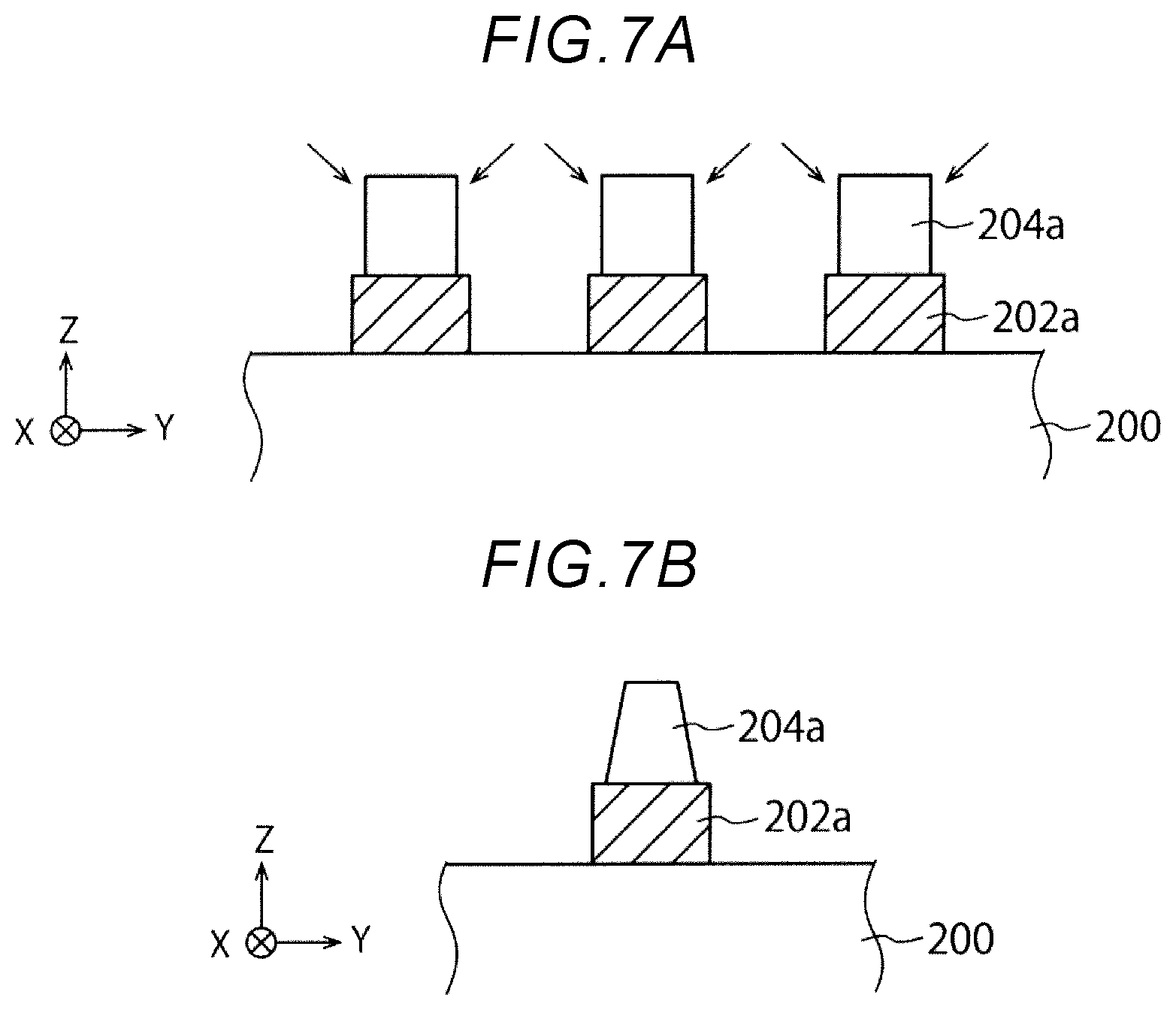
[0051] Next, a method of manufacturing the semiconductor memory device according to the second embodiment will be described with reference to FIG. 7A. The same steps explained in FIG. 5A and FIG. 5B for the semiconductor memory device according to the first embodiment are performed. Thereafter, as shown in FIG. 7A, the pattern 204a is irradiated with an ion beam from a direction inclined with respect to a stacking direction (i.e., the z direction) to slim the pattern 204a. The slimming is performed to reduce the length of the pattern 204a in the y direction. Alternatively, the slimming may be performed to reduce the length of the pattern 204a in the x direction. Further, the lengths of the patterns 204a in the x direction and the y direction may be reduced, separately.
[0052] Thereafter, the steps described in FIG. 5C to FIG. 5F are performed, and then the steps shown in FIG. 5A to FIG. 5F are repeated. At this time, in the step shown in FIG. 5C, the interlayer insulating film 206 is formed instead of forming the insulating film 208. Further, the memory cell of the uppermost layer semiconductor memory is slimmed.
[0053] In the second embodiment, as shown in FIG. 7B, the pattern 204a to be the storage layer 12b.sub.i may have a tapered shape in which a length in the y direction decreases from a lower surface to an upper surface. That is, the pattern 204a to be the storage layer 12b.sub.i may have a tapered shape in which an area of a cross section cut along the x-y plane decreases from the lower surface to the upper surface. In the pattern 204a to be the storage layer 12b.sub.i, the length of the lower surface in the y direction may be longer than the length of the upper surface in the y direction. In addition, in the pattern 204a to be the storage layer 12b.sub.i, the area of the lower surface may be larger than the area of the upper surface.
Third Embodiment
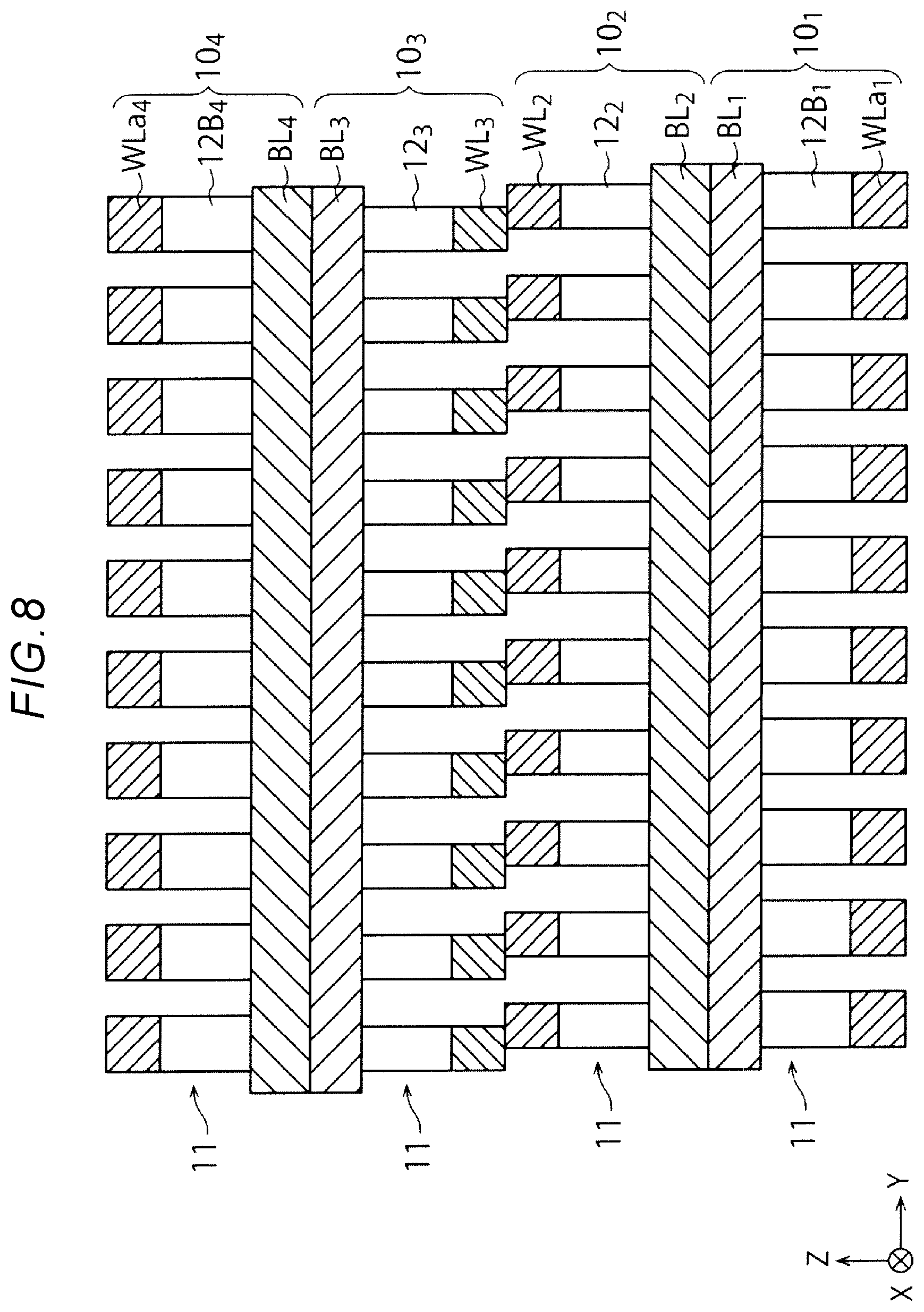
[0054] A semiconductor memory device according to a third embodiment is shown in FIG. 8. In the semiconductor memory device of the third embodiment, with respect to the semiconductor memory device according to the first embodiment shown in FIG. 2, the insulating film 13a having a high heat insulating property from the first semiconductor memory 10.sub.1 is removed, the insulating film 13b having a high heat insulating property from the fourth semiconductor memory 10.sub.4 is removed, the word line WL.sub.1 of the first semiconductor memory 10.sub.1 is replaced with a word line WLa.sub.1, the storage unit 12.sub.1 is replaced with a storage unit 12B.sub.1, the word line WL.sub.4 of the fourth semiconductor memory 10.sub.4 is replaced with a word line WLa.sub.4, and the storage unit 12.sub.4 is replaced with a storage unit 12B.sub.4.
[0055] As compared with the word line WL.sub.2 and the word line WL.sub.3, the word line WLa.sub.1 and the word line WLa.sub.4 are larger in width, that is, a length in the y direction is long, and are larger in thickness, that is, a length in the z direction is long. The lengths of the storage unit 12B.sub.1 and the storage unit 12B.sub.4 are longer than those of the storage unit 12.sub.2 and the storage unit 12.sub.3 in the y direction. The lengths of the storage units 12B.sub.1 and the storage units 12B.sub.4 in the y direction are respectively the same as the lengths of the word line WLa.sub.1 and the word line WLa.sub.4 in the y direction. This is because the storage units 12B.sub.1 and 12B.sub.4 and the word lines WLa.sub.1 and WLa.sub.4 are processed (i.e., patterned) by using the same mask. However, the storage units 12B.sub.1 and 12B.sub.4 and the word lines WLa.sub.1 and WLa.sub.4 do not need to have the same length.
[0056] In the third embodiment, the lengths of the word line WLa.sub.1 and the word line WLa.sub.4 are longer than those of the word lines WL.sub.2 and WL.sub.3 in the y and z directions. Therefore, the wiring resistance can be reduced as compared with the semiconductor memory device shown in FIG. 1, and although the reset current of the memory cells 11 of the first semiconductor memory 10.sub.1 and the fourth semiconductor memory 10.sub.4 is increased as compared with the second and the third semiconductor memories 10.sub.2 and 10.sub.3, the reset operation is stable, and reliability of the reset operation can be increased. In the third embodiment, the lengths of the word line WLa.sub.1 and the word line WLa.sub.4 are longer than those of the word lines WL.sub.2 and WL.sub.3 in both the y and z directions, but only the lengths in the y direction may be increased.
[0057] Even when the word line WLa.sub.1 and the word line WLa.sub.4 have the same length as the word lines WL.sub.2 and WL.sub.3 in the y and z directions and are formed by using a material having an electric conductivity higher than that of the word lines WL.sub.2 and WL.sub.3, the same effect can be obtained.
[0058] In addition, in the third embodiment shown in FIG. 8, the word line WL.sub.2 and the word line WL.sub.3 may be misaligned, but only a part thereof overlaps. This is because misalignment occurs between the mask that forms the word line WL.sub.2 and the mask that forms the word line WL.sub.3.
Fourth Embodiment
[0059] A semiconductor memory device according to a fourth embodiment is shown in FIG. 9. In the semiconductor memory device according to the fourth embodiment, with respect to the semiconductor memory device according to the first embodiment shown in FIG. 2, the insulating film 13a having a high heat insulating property from the first semiconductor memory 10.sub.1 is removed, the insulating film 13b having a high heat insulating property from the fourth semiconductor memory 10.sub.4 is removed, the word line WL.sub.1 of the first semiconductor memory 10.sub.1 is replaced with a word line WLb.sub.1, and the word line WL.sub.4 of the fourth semiconductor memory 10.sub.4 is replaced with a word line WLb.sub.4.
[0060] The lengths of the word line WLb.sub.1 and the word line WLb.sub.4 in the z direction are longer than, for example, twice longer the lengths of the word line WL.sub.2 and the word line WL.sub.3 in the z direction. Therefore, formation of the word line WLb.sub.1 and the word line WLb.sub.4 is performed by repeating the steps same as the steps of forming the word line WL.sub.2 or the word line WL.sub.3 twice.
[0061] In the fourth embodiment, the lengths of the word line WLb.sub.1 and the word line WLb.sub.4 are longer than those of the word lines WL.sub.2 and WL.sub.3 in the z direction. Therefore, the wiring resistance can be reduced as compared with the semiconductor memory device shown in FIG. 1. Accordingly, the reset operation is stable, and reliability of the reset operation can be improved.
[0062] Even when the word line WLb.sub.1 and the word line WLb.sub.4 have the same length as the word lines WL.sub.2 and WL.sub.3 in the z direction and are formed by using a material having an electric conductivity high than that of the word lines WL.sub.2 and WL.sub.3, the same effect can be obtained.
[0063] As described above, the semiconductor memory device according to any one of the first to fourth embodiments can increase the reliability of the reset operation.
[0064] While certain embodiments have been described, these embodiments have been presented by way of example only, and are not intended to limit the scope of the inventions. Indeed, the novel embodiments described herein may be embodied in a variety of other forms; furthermore, various omissions, substitutions and changes in the form of the embodiments described herein may be made without departing from the spirit of the inventions. The accompanying claims and their equivalents are intended to cover such forms or modifications as would fall within the scope and spirit of the inventions.
* * * * *
D00000
D00001
D00002
D00003
D00004
D00005
D00006
D00007
D00008
D00009
D00010
D00011
XML
uspto.report is an independent third-party trademark research tool that is not affiliated, endorsed, or sponsored by the United States Patent and Trademark Office (USPTO) or any other governmental organization. The information provided by uspto.report is based on publicly available data at the time of writing and is intended for informational purposes only.
While we strive to provide accurate and up-to-date information, we do not guarantee the accuracy, completeness, reliability, or suitability of the information displayed on this site. The use of this site is at your own risk. Any reliance you place on such information is therefore strictly at your own risk.
All official trademark data, including owner information, should be verified by visiting the official USPTO website at www.uspto.gov. This site is not intended to replace professional legal advice and should not be used as a substitute for consulting with a legal professional who is knowledgeable about trademark law.