Holographic Waveguide Backlight and Related Methods of Manufacturing
Waldern; Jonathan David ; et al.
U.S. patent application number 16/817524 was filed with the patent office on 2020-09-17 for holographic waveguide backlight and related methods of manufacturing. This patent application is currently assigned to DigiLens Inc.. The applicant listed for this patent is Digilens Inc.. Invention is credited to Alastair John Grant, Milan Popovich, Jonathan David Waldern.
| Application Number | 20200292745 16/817524 |
| Document ID | / |
| Family ID | 1000004722876 |
| Filed Date | 2020-09-17 |

| United States Patent Application | 20200292745 |
| Kind Code | A1 |
| Waldern; Jonathan David ; et al. | September 17, 2020 |
Holographic Waveguide Backlight and Related Methods of Manufacturing
Abstract
Systems and methods for holographic waveguide backlights in accordance with various embodiments of the invention are illustrated. One embodiment includes an optical illumination device including at least one waveguide, a source of light optically coupled to the at least one waveguide configured to emit light having a first polarization state, a first plurality of grating elements for diffracting the light having the first polarization state out of the at least one waveguide into a first set of output paths, a second plurality of grating elements for diffracting the light having the first polarization state light out of the at least one waveguide into a second set of output paths, and at least one input coupler configured to couple at least a portion of the light having the first polarization state towards the first and second pluralities of grating elements.
| Inventors: | Waldern; Jonathan David; (Los Altos Hills, CA) ; Popovich; Milan; (Leicester, GB) ; Grant; Alastair John; (San Jose, CA) | ||||||||||
| Applicant: |
|
||||||||||
|---|---|---|---|---|---|---|---|---|---|---|---|
| Assignee: | DigiLens Inc. Sunnyvale CA |
||||||||||
| Family ID: | 1000004722876 | ||||||||||
| Appl. No.: | 16/817524 | ||||||||||
| Filed: | March 12, 2020 |
Related U.S. Patent Documents
| Application Number | Filing Date | Patent Number | ||
|---|---|---|---|---|
| 62817468 | Mar 12, 2019 | |||
| Current U.S. Class: | 1/1 |
| Current CPC Class: | G02B 6/0056 20130101; G02B 5/32 20130101; G02B 6/0035 20130101 |
| International Class: | F21V 8/00 20060101 F21V008/00; G02B 5/32 20060101 G02B005/32 |
Claims
1. An optical illumination device comprising: a light guiding structure with an upper surface for extracting illumination and a lower surface; a light source optically coupled to said light guiding structure and configured to provide polarized light, said light undergoing total internal reflection within said light guiding structure; and at least one plurality of grating elements disposed in at least one grating layer for extracting light from said light guiding structure.
2. The optical illumination device of claim 1, wherein said light source is configured to emit at least first and second wavelength collimated light color sequentially, wherein said at least one plurality of grating elements comprises a first plurality of grating elements for diffracting said first wavelength light out of said light guiding structure into a first set of output paths, and a second plurality grating elements for diffracting said second wavelength light out of said light guiding structure into a second set of output paths substantially overlapping said first set of output paths.
3. The optical illumination device of claim 2, further comprising a substrate having half-wave retarding regions interspersed with clear regions overlaying said upper surface, wherein each said half wave retarding region overlaps at least one grating element in each of said first and second pluralities of grating elements; and wherein each said clear region overlaps at least one grating element in each of said first and second pluralities of grating elements.
4. The optical illumination device of claim 2, further comprising a quarter-wave retarding layer disposed, said quarter-wave retarding layer having a first surface disposed in proximity to said lower surface and a reflective surface.
5. The optical illumination device of claim 2, wherein said first plurality of grating elements is disposed in a separate grating layer to said second plurality of grating elements, wherein grating elements for diffracting said first wavelength light overlap grating elements for diffracting said second wavelength light.
6. The optical illumination device of claim 2, wherein grating elements for diffracting first and second wavelength light are disposed as uniformly interspersed first and second multiplicities of grating elements in one layer.
7. The optical illumination device of claim 2, wherein grating elements for diffracting first and second wavelength light are disposed as uniformly interspersed first and second multiplicities of grating elements in two layers, wherein grating element for diffracting a first wavelength light overlap grating elements for diffracting second wavelength light.
8. The optical illumination device of claim 2, wherein grating elements for diffracting first wavelength light have a first grating vector and grating elements for diffracting second wavelength light have a second grating vector in an opposing direction to said first grating vector.
9. The optical illumination device of claim 2, wherein grating elements for diffracting first wavelength light and grating elements for diffracting second wavelength light have grating vectors aligned in substantially parallel directions.
10. The optical illumination device of claim 2, wherein grating elements for diffracting first wavelength light and grating elements for diffracting second wavelength light are off-Bragg with respect to each other.
11. The optical illumination device of claim 2, wherein grating elements for diffracting first wavelength light are disposed in a first layer in which grating elements having a first grating vector and grating elements having a second grating vector in an opposing direction to said first grating vector are uniformly interspersed, wherein grating elements for diffracting second wavelength light are disposed in a second layer in which grating elements having a first grating vector and grating elements having a second grating vector in an opposing direction to said first grating vector are interspersed.
12. The optical illumination device of claim 2, wherein said first wavelength light has a first polarization and said second wavelength light has a second polarization orthogonal to said first polarization.
13. The optical illumination device of claim 2, wherein said first wavelength light and said second wavelength light have the same polarization.
14. The optical illumination device of claim 2, wherein grating elements for diffracting first and second wavelength light are disposed as first and second multiplicities of grating elements multiplexed in a single layer, wherein grating elements for diffracting said first wavelength are multiplexed with grating elements for diffracting said second wavelength light.
15. The optical illumination device of claim 2, wherein grating elements for diffracting first and second wavelength light are disposed as first and second multiplicities of grating elements in a stack of two contacting layers with grating elements for diffracting said first wavelength light overlapping grating elements for diffracting said second wavelength light.
16. The optical illumination device of claim 2, wherein grating elements of said first plurality are switched into a diffracting state when said light source emits said first wavelength light and grating elements of said second plurality are switched into a diffracting state when said light source emits said second wavelength light.
17. The optical illumination device of claim 2, wherein said output paths are angularly separated.
18. The optical illumination device of claim 2, wherein said output paths are substantially normal to said upper surface.
19. The optical illumination device of claim 1, wherein said at least one plurality of grating elements is disposed in at least one grating layer, wherein said light guiding structure comprises at least one waveguide, wherein each said waveguide supports at least one of said grating layers.
20. The optical illumination device of claim 1, wherein said layer is formed between transparent substrates with transparent conductive coatings applied to each said substrate, at least one of said coatings being patterned into independently addressable elements overlapping said grating elements, wherein an electrical control circuit operative to apply voltages across each said grating elements is provided.
21. The optical illumination device of claim 1, wherein each said grating element comprises at least one property selected from the group consisting of: a planar Bragg surfaces, optical power, optical retardation, diffusing properties, spatially varying diffraction efficiency, diffraction efficiency proportional to a voltage applied across said grating element, and phase retardation proportional to a voltages applied across said grating element.
22. The optical illumination device of claim 1, wherein said at least one plurality of grating elements comprises a two-dimensional array.
23. The optical illumination device of claim 1, wherein said at least one plurality of grating elements comprises a one-dimensional array of elongate elements.
24. The optical illumination device of claim 1, wherein each said grating element is recorded in a Holographic Polymer Dispersed Liquid Crystal.
25. The optical illumination device of claim 1, wherein said light is coupled into said light guide structure by a grating or a prism.
26. The optical illumination device of claim 1, wherein said light source is laser or LED.
27. The optical illumination device of claim 1, further comprising at least one component selected from the group consisting of: a beam deflector, a dichroic filter, a microlens array, beam shaper, light integrator, and a polarization rotator.
Description
CROSS-REFERENCE TO RELATED APPLICATIONS
[0001] The current application claims the benefit of and priority under 35 U.S.C. .sctn. 119(e) to U.S. Provisional Patent Application No. 62/817,468 entitled "Holographic Waveguide Backlight," filed Mar. 12, 2019. The disclosure of U.S. Provisional Patent Application No. 62/817,468 is hereby incorporated by reference in its entirety for all purposes.
FIELD OF THE INVENTION
[0002] The present invention generally relates to waveguide devices and, more specifically, to holographic waveguide backlights.
BACKGROUND
[0003] Waveguides can be referred to as structures with the capability of confining and guiding waves (i.e., restricting the spatial region in which waves can propagate). One subclass includes optical waveguides, which are structures that can guide electromagnetic waves, typically those in the visible spectrum. Waveguide structures can be designed to control the propagation path of waves using a number of different mechanisms. For example, planar waveguides can be designed to utilize diffraction gratings to diffract and couple incident light into the waveguide structure such that the in-coupled light can proceed to travel within the planar structure via total internal reflection (TIR).
[0004] Fabrication of waveguides can include the use of material systems that allow for the recording of holographic optical elements within the waveguides. One class of such material includes polymer dispersed liquid crystal (PDLC) mixtures, which are mixtures containing photopolymerizable monomers and liquid crystals. A further subclass of such mixtures includes holographic polymer dispersed liquid crystal (HPDLC) mixtures. Holographic optical elements, such as volume phase gratings, can be recorded in such a liquid mixture by illuminating the material with two mutually coherent laser beams. During the recording process, the monomers polymerize, and the mixture undergoes a photopolymerization-induced phase separation, creating regions densely populated by liquid crystal micro-droplets, interspersed with regions of clear polymer. The alternating liquid crystal-rich and liquid crystal-depleted regions form the fringe planes of the grating. The resulting grating, which is commonly referred to as a switchable Bragg grating (SBG), has all the properties normally associated with volume or Bragg gratings but with much higher refractive index modulation ranges combined with the ability to electrically tune the grating over a continuous range of diffraction efficiency (the proportion of incident light diffracted into a desired direction). The latter can extend from non-diffracting (cleared) to diffracting with close to 100% efficiency.
[0005] Waveguide optics, such as those described above, can be considered for a range of display and sensor applications. In many applications, waveguides containing one or more grating layers encoding multiple optical functions can be realized using various waveguide architectures and material systems, enabling new innovations in near-eye displays for augmented reality (AR) and virtual reality (VR), compact head-up displays (HUDs) and helmet-mounted displays or head-mounted displays (HMDs) for road transport, aviation, and military applications, and sensors for biometric and laser radar (LIDAR) applications.
SUMMARY OF THE INVENTION
[0006] Systems and methods for holographic waveguide backlights in accordance with various embodiments of the invention are illustrated. One embodiment includes an optical illumination device including a light guiding structure with an upper surface for extracting illumination and a lower surface, a light source optically coupled to the light guiding structure and configured to provide polarized light, the light undergoing total internal reflection within the light guiding structure, and at least one plurality of grating elements disposed in at least one grating layer for extracting light from the light guiding structure.
[0007] In another embodiment, the light source is configured to emit at least first and second wavelength collimated light color sequentially, wherein the at least one plurality of grating elements includes a first plurality of grating elements for diffracting the first wavelength light out of the light guiding structure into a first set of output paths, and a second plurality grating elements for diffracting the second wavelength light out of the light guiding structure into a second set of output paths substantially overlapping the first set of output paths.
[0008] In a further embodiment, the optical illumination device further includes a substrate having half-wave retarding regions interspersed with clear regions overlaying the upper surface, wherein each the half wave retarding region overlaps at least one grating element in each of the first and second pluralities of grating elements, and each the clear region overlaps at least one grating element in each of the first and second pluralities of grating elements.
[0009] In still another embodiment, the optical illumination device further includes a quarter-wave retarding layer disposed, the quarter-wave retarding layer having a first surface disposed in proximity to the lower surface and a reflective surface.
[0010] In a still further embodiment, the first plurality of grating elements is disposed in a separate grating layer to the second plurality of grating elements, wherein grating elements for diffracting the first wavelength light overlap grating elements for diffracting the second wavelength light.
[0011] In yet another embodiment, grating elements for diffracting first and second wavelength light are disposed as uniformly interspersed first and second multiplicities of grating elements in one layer.
[0012] In a yet further embodiment, grating elements for diffracting first and second wavelength light are disposed as uniformly interspersed first and second multiplicities of grating elements in two layers, wherein grating element for diffracting a first wavelength light overlap grating elements for diffracting second wavelength light.
[0013] In another additional embodiment, grating elements for diffracting first wavelength light have a first grating vector and grating elements for diffracting second wavelength light have a second grating vector in an opposing direction to the first grating vector.
[0014] In a further additional embodiment, grating elements for diffracting first wavelength light and grating elements for diffracting second wavelength light have grating vectors aligned in substantially parallel directions.
[0015] In another embodiment again, grating elements for diffracting first wavelength light and grating elements for diffracting second wavelength light are off-Bragg with respect to each other.
[0016] In a further embodiment again, grating elements for diffracting first wavelength light are disposed in a first layer in which grating elements having a first grating vector and grating elements having a second grating vector in an opposing direction to the first grating vector are uniformly interspersed, wherein grating elements for diffracting second wavelength light are disposed in a second layer in which grating elements having a first grating vector and grating elements having a second grating vector in an opposing direction to the first grating vector are interspersed.
[0017] In still yet another embodiment, the first wavelength light has a first polarization and the second wavelength light has a second polarization orthogonal to the first polarization.
[0018] In a still yet further embodiment, the first wavelength light and the second wavelength light have the same polarization.
[0019] In still another additional embodiment, grating elements for diffracting first and second wavelength light are disposed as first and second multiplicities of grating elements multiplexed in a single layer, wherein grating elements for diffracting the first wavelength are multiplexed with grating elements for diffracting the second wavelength light.
[0020] In a still further additional embodiment, grating elements for diffracting first and second wavelength light are disposed as first and second multiplicities of grating elements in a stack of two contacting layers with grating elements for diffracting the first wavelength light overlapping grating elements for diffracting the second wavelength light.
[0021] In still another embodiment again, grating elements of the first plurality are switched into a diffracting state when the light source emits the first wavelength light and grating elements of the second plurality are switched into a diffracting state when the light source emits the second wavelength light.
[0022] In a still further embodiment again, the output paths are angularly separated.
[0023] In yet another additional embodiment, the output paths are substantially normal to the upper surface.
[0024] In a yet further additional embodiment, the at least one plurality of grating elements is disposed in at least one grating layer, wherein the light guiding structure includes at least one waveguide, wherein each the waveguide supports at least one of the grating layers.
[0025] In yet another embodiment again, the layer is formed between transparent substrates with transparent conductive coatings applied to each the substrate, at least one of the coatings being patterned into independently addressable elements overlapping the grating elements, wherein an electrical control circuit operative to apply voltages across each the grating elements is provided.
[0026] In a yet further embodiment again, each the grating element includes at least one property that is one of a planar Bragg surfaces, optical power, optical retardation, diffusing properties, spatially varying diffraction efficiency, diffraction efficiency proportional to a voltage applied across the grating element, and phase retardation proportional to a voltages applied across the grating element.
[0027] In another additional embodiment again, the at least one plurality of grating elements includes a two-dimensional array.
[0028] In a further additional embodiment again, the at least one plurality of grating elements includes a one-dimensional array of elongate elements.
[0029] In still yet another additional embodiment, each the grating element is recorded in a Holographic Polymer Dispersed Liquid Crystal.
[0030] In a still yet further additional embodiment, the light is coupled into the light guide structure by a grating or a prism.
[0031] In yet another additional embodiment again, the light source is laser or LED.
[0032] In a yet further additional embodiment again, the optical illumination device further includes at least one component that is one of a beam deflector, a dichroic filter, a microlens array, beam shaper, light integrator, and a polarization rotator.
[0033] A still yet another embodiment again includes an optical illumination device including at least one waveguide, a source of light optically coupled to the at least one waveguide configured to emit light having a first polarization state, a first plurality of grating elements for diffracting the light having the first polarization state out of the at least one waveguide into a first set of output paths, a second plurality of grating elements for diffracting the light having the first polarization state light out of the at least one waveguide into a second set of output paths, and at least one input coupler configured to couple at least a portion of the light having the first polarization state towards the first and second pluralities of grating elements.
[0034] In a still yet further embodiment again, the optical illumination device further includes a quarter-wave plate having a reflective surface, and a substrate including a plurality of transparent regions and a plurality of regions supporting half-wave plates, wherein at least one of the first plurality of grating elements is configured to diffract a first portion of the light having the first polarization state towards at least one of the plurality of transparent regions, at least one of the second plurality of grating elements is configured to diffract a second portion of the light having the first polarization state towards the quarter-wave plate, and the quarter-wave plate is configured to reflect incident the light having the first polarization state towards at least one of the plurality of regions supporting half-wave plates, wherein the reflected incident light has its polarization state changed to a second polarization state that is orthogonal to the first polarization state, wherein the first and second pluralities of grating elements are formed in at least one grating layer disposed within the at least one waveguide.
[0035] In still yet another additional embodiment again, the optical illumination device further includes third and fourth pluralities of grating elements, wherein the light having a first polarization state includes light of a first wavelength band and light of a second wavelength band, the at least one input coupler includes a first input coupler for coupling the light of the first wavelength band towards the first and second pluralities of grating elements, and a second input coupler for coupling the light of the second wavelength band towards the third and fourth pluralities of grating elements.
[0036] In a still yet further additional embodiment again, the at least one waveguide includes first and second grating layers, the first and second pluralities of grating elements are interspersed within the first grating layer, the third and fourth pluralities of grating elements are interspersed with the second grating layer, the first and third pluralities of grating elements have grating vectors in a first direction, and the second and fourth pluralities of grating elements have grating vectors in an opposing direction to the first direction.
[0037] In still another additional embodiment again, the emitted light is collimated light, and source of light is configured to emit the light of the first and second wavelength bands sequentially.
[0038] In a still further additional embodiment again, the first and second pluralities of grating elements are configured to switch into a diffracting state when the source of light emits the light of the first wavelength band is emitted, and the third and fourth pluralities of grating elements are configured to switch into a diffracting state when the source of light emits the light of the second wavelength band.
[0039] In yet another additional embodiment again, the optical illumination device further includes third and fourth pluralities of grating elements, wherein the at least one waveguide includes first and second grating layers, the first and third pluralities of grating elements are interspersed within the first grating layer, the second and fourth pluralities of grating elements are interspersed within the second grating layer, the light having a first polarization state includes light of a first wavelength band and light of a second wavelength band, and the at least one input coupler includes a first input coupler for coupling the light of the first wavelength band towards the first and second pluralities of grating elements, and a second input coupler for coupling the light of the second wavelength band towards the third and fourth pluralities of grating elements.
[0040] In a yet further additional embodiment again, the optical illumination device further includes a quarter-wave plate having a reflective surface, third and fourth pluralities of grating elements, wherein the source of light is further configured to emit light having a second polarization state, the light having the first polarization state is in a first wavelength band, and the light having the second polarization state is in a second wavelength band, the third and fourth pluralities of grating elements are configured to diffract the light having the second polarization state towards the quarter-wave plate, the at least one waveguide includes first and second grating layers, the first and third pluralities of grating elements are interspersed within the first grating layer, and the second and fourth pluralities of grating elements are interspersed within the second grating layer, and the first plurality of grating elements spatially overlaps the second plurality of grating elements.
[0041] In still yet another additional embodiment again, the first plurality of grating elements has a grating vector in a first direction, and the second plurality of grating elements has a grating vector in an opposing direction to the first direction.
[0042] In a still yet further additional embodiment again, the source of light is a laser source.
[0043] Additional embodiments and features are set forth in part in the description that follows, and in part will become apparent to those skilled in the art upon examination of the specification or may be learned by the practice of the invention. A further understanding of the nature and advantages of the present invention may be realized by reference to the remaining portions of the specification and the drawings, which forms a part of this disclosure.
BRIEF DESCRIPTION OF THE DRAWINGS
[0044] The description will be more fully understood with reference to the following figures and data graphs, which are presented as exemplary embodiments of the invention and should not be construed as a complete recitation of the scope of the invention.
[0045] FIGS. 1A and 1B conceptually illustrate HPDLC SBG devices and the switching property of SBGs in accordance with various embodiments of the invention.
[0046] FIG. 2 conceptually illustrates a waveguide backlight in accordance with an embodiment of the invention.
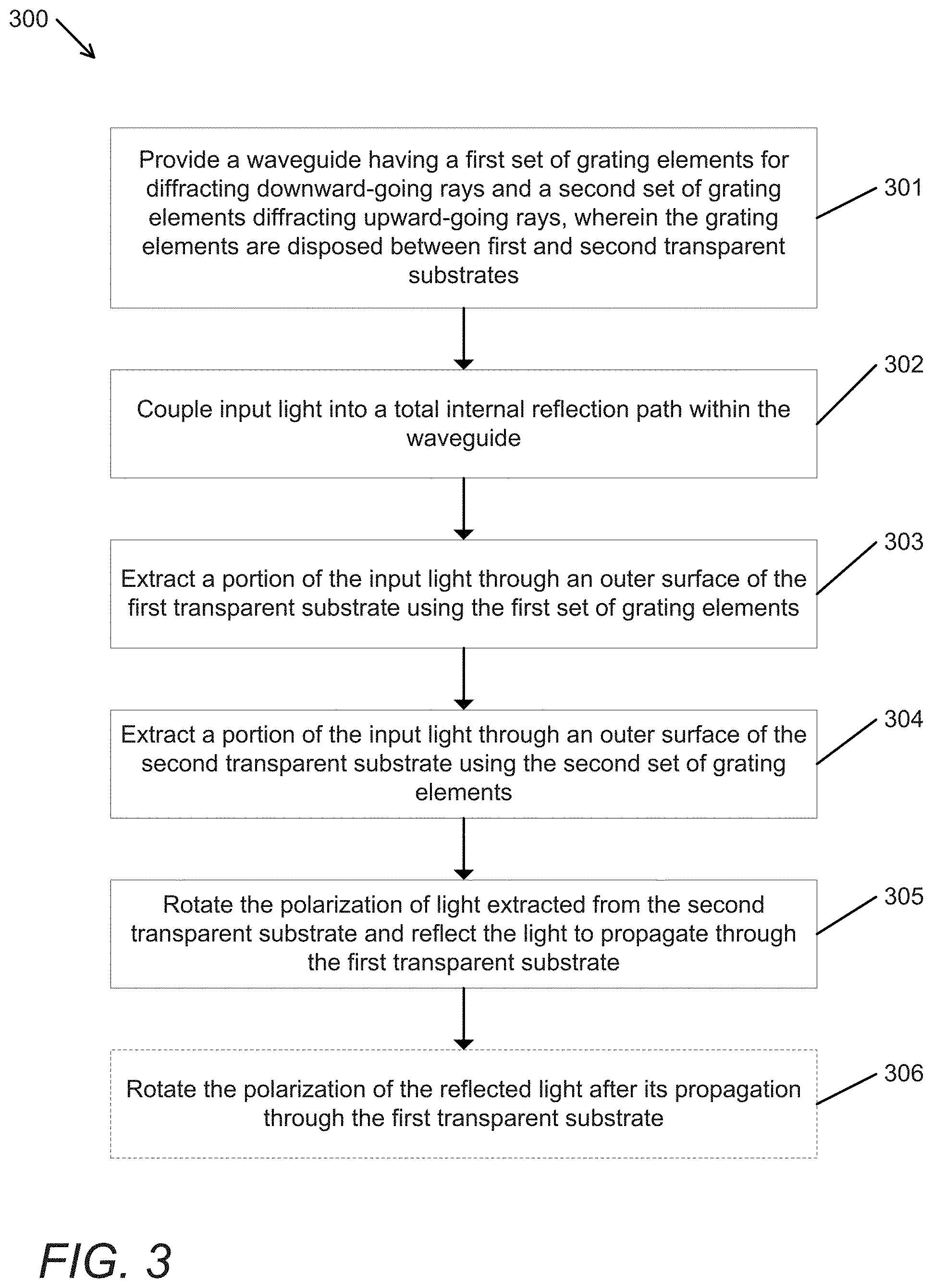
[0047] FIG. 3 conceptually illustrates a flow chart of a process for providing a waveguide backlight in accordance with an embodiment of the invention.
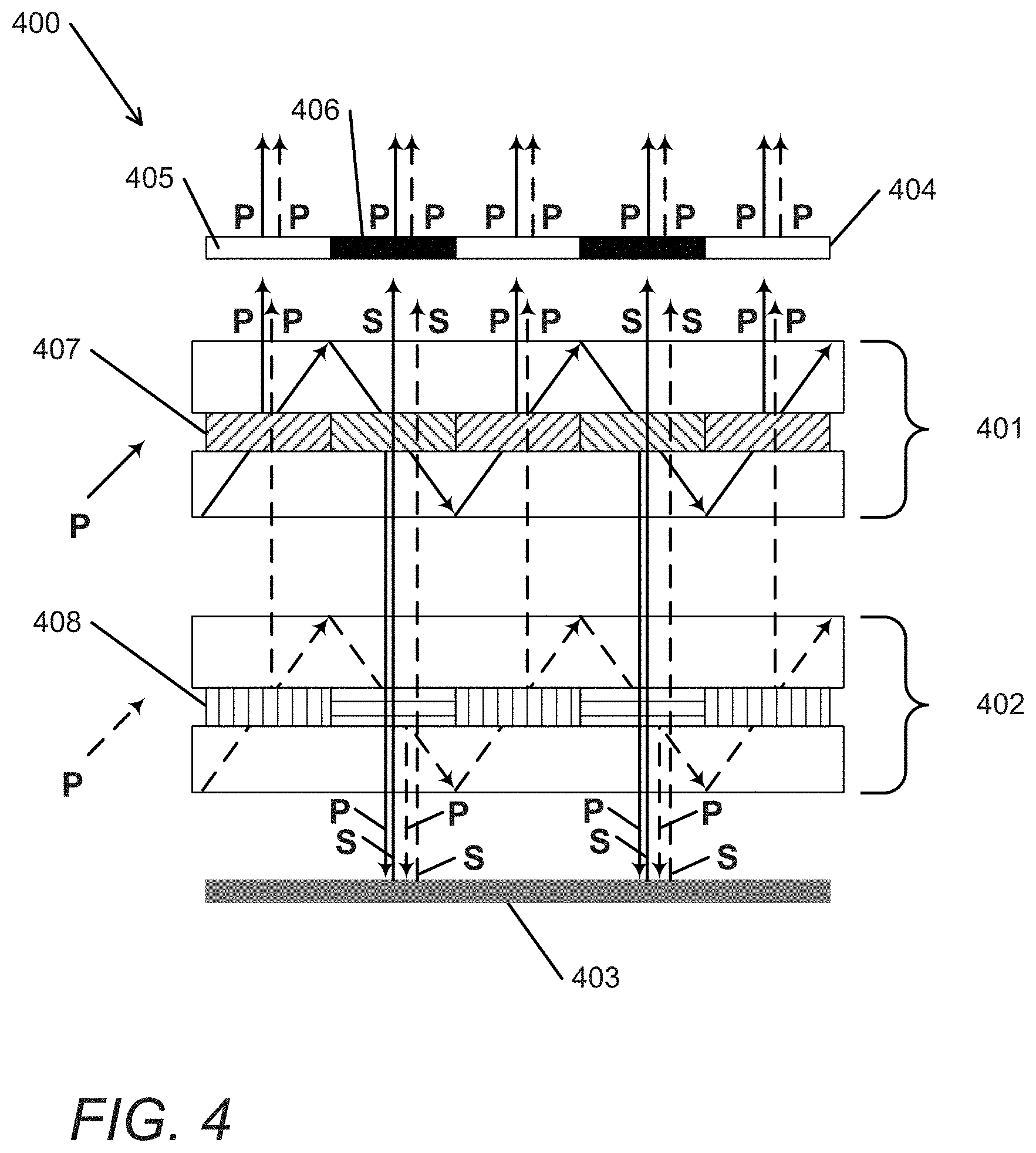
[0048] FIG. 4 conceptually illustrates a waveguide backlight with two waveguide layers in accordance with an embodiment of the invention.
[0049] FIG. 5 conceptually illustrates a waveguide backlight with a single waveguide layer in accordance with an embodiment of the invention.
[0050] FIG. 6 conceptually illustrates a waveguide backlight having two waveguide layers with alternating wavelength-diffracting grating elements in accordance with an embodiment of the invention.
[0051] FIG. 7 conceptually illustrates a waveguide backlight having a single waveguide layer with alternating wavelength-diffracting grating elements in accordance with an embodiment of the invention.
[0052] FIG. 8 conceptually illustrates a waveguide backlight having two waveguide layers with alternating wavelength-diffracting grating elements for input light having orthogonal polarizations in accordance with an embodiment of the invention.
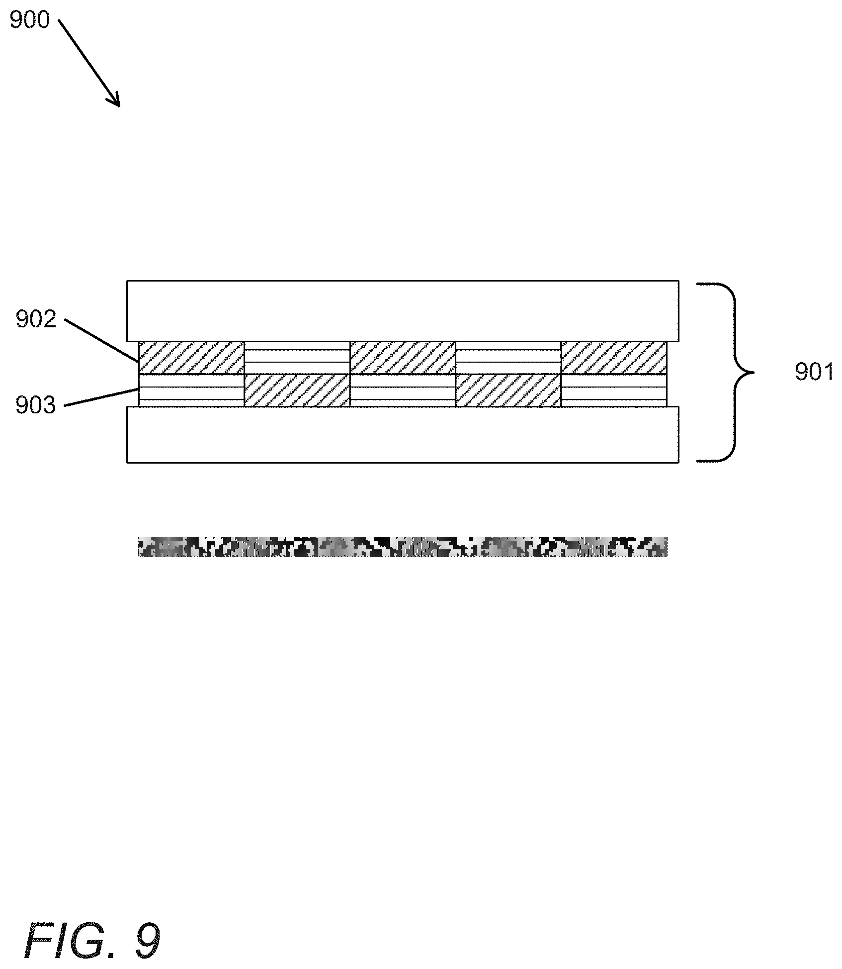
[0053] FIG. 9 conceptually illustrates a waveguide backlight having a single waveguide layer with alternating wavelength-diffracting grating elements for input light having orthogonal polarizations in accordance with an embodiment of the invention.
DETAILED DESCRIPTION
[0054] For the purposes of describing embodiments, some well-known features of optical technology known to those skilled in the art of optical design and visual displays have been omitted or simplified in order to not obscure the basic principles of the invention. Unless otherwise stated, the term "on-axis" in relation to a ray or a beam direction refers to propagation parallel to an axis normal to the surfaces of the optical components described in relation to the invention. In the following description the terms light, ray, beam, and direction may be used interchangeably and in association with each other to indicate the direction of propagation of electromagnetic radiation along rectilinear trajectories. The term light and illumination may be used in relation to the visible and infrared bands of the electromagnetic spectrum. Parts of the following description will be presented using terminology commonly employed by those skilled in the art of optical design. As used herein, the term grating may encompass a grating comprised of a set of gratings in some embodiments. For illustrative purposes, it is to be understood that the drawings are not drawn to scale unless stated otherwise.
[0055] An ideal backlight unit (BLU) should have a compact (i.e., thin) form factor and should deliver uniform luminance and color with efficient coupling of light from the illumination source and extraction from the BLU onto the display panel to be back-lit. In mobile displays, the BLU thickness should be a few millimeters. Television displays likewise require low thickness to image diagonal ratios. Traditional edge-lit solutions have failed to meet form factor and uniformity requirements. Waveguide or light guiding, which carry the illumination light by total internal reflection while extracting portions of such light from the waveguide, can provide very thin form factors. However, waveguides can suffer from spatial variations of luminance and color due to the dispersive properties of gratings typically implemented in waveguides. In some cases, dispersion can be greatly alleviated by using laser sources.
[0056] Illumination nonuniformities can arise from wavelength-dependent absorption within gratings; the small loss incurred at each beam-grating interaction can be multiplied as the beam propagates down the waveguide, leading to a progressive dimming of light along the waveguide. Where laser sources are used, which can make for a very compact light source-to-waveguide coupling optics, the high coherence of the lasers can result in a banding effect caused by gaps or overlaps due to imperfect interlacing of the total internal reflection beams. Laser-lit BLUs can also suffer from laser speckle. Another source of nonuniformity, when birefringent materials are used to form gratings, results from polarization rotations occurring at each beam bounce. This polarization variation can manifest itself as luminance nonuniformity. Color nonuniformity can also occur due to wavelength dependence of birefringence. Finally, birefringent gratings can result in spatially varying polarization at the output of the BLU. This can result in luminance and color nonuniformity when the display panel to be lit is a liquid crystal device.
[0057] Turning now to the drawings, holographic waveguide backlight in accordance with various embodiments of the invention are illustrated. In many embodiments, the waveguide backlight is implemented as a compact, efficient, highly uniform, color waveguide backlight that can be used in a range of display applications, such as but not limited to LCD monitors, digital holographic display, and mobile computing and telecommunications devices. In many embodiments, the waveguide backlight includes a waveguide and a source of light configured to provide input light. The input light can be coupled into the waveguide in a total internal reflection path using a variety of different methods. In some embodiments, an input coupler, such as but not limited to a grating or a prism, is utilized to couple light into the waveguide. In several embodiments, the source of light is configured to provide light of different wavelengths. In further embodiments, the source of light is configured to emit at least first and second wavelength collimated light color sequentially. The waveguide can include at least two sets of grating elements disposed across at least one grating layer. Each set of grating elements can be configured to operate at a specific wavelength/angular band. In many embodiments, each set of grating elements is configured to diffract and extract either upward-going or downward-going light. In several embodiments, each set of grating elements are configured for a specific wavelength band. In further embodiments, each set of grating elements include switchable Bragg gratings and is switched into a diffracting state when the light source emits wavelength light intended for that set. In some embodiments, waveplates and retarders are implemented to control the polarization of light. As can readily be appreciated, waveguide backlights in accordance with various embodiments of the invention can be implemented in numerous configurations, the specific of which can depend on the application. Waveguide backlight configurations, optical waveguide structures, materials, and manufacturing processes are discussed in the sections below in further detail.
Optical Waveguide and Grating Structures
[0058] Optical structures recorded in waveguides can include many different types of optical elements, such as but not limited to diffraction gratings. Gratings can be implemented to perform various optical functions, including but not limited to coupling light, directing light, and preventing the transmission of light. In many embodiments, the gratings are surface relief gratings that reside on the outer surface of the waveguide. In other embodiments, the grating implemented is a Bragg grating (also referred to as a volume grating), which are structures having a periodic refractive index modulation. Bragg gratings can be fabricated using a variety of different methods. One process includes interferential exposure of holographic photopolymer materials to form periodic structures. Bragg gratings can have high efficiency with little light being diffracted into higher orders. The relative amount of light in the diffracted and zero order can be varied by controlling the refractive index modulation of the grating, a property that can be used to make lossy waveguide gratings for extracting light over a large pupil.
[0059] One class of Bragg gratings used in holographic waveguide devices is the Switchable Bragg Grating (SBG). SBGs can be fabricated by first placing a thin film of a mixture of photopolymerizable monomers and liquid crystal material between substrates. The substrates can be made of various types of materials, such glass and plastics. In many cases, the substrates are in a parallel configuration. In other embodiments, the substrates form a wedge shape. One or both substrates can support electrodes, typically transparent tin oxide films, for applying an electric field across the film. The grating structure in an SBG can be recorded in the liquid material (often referred to as the syrup) through photopolymerization-induced phase separation using interferential exposure with a spatially periodic intensity modulation. Factors such as but not limited to control of the irradiation intensity, component volume fractions of the materials in the mixture, and exposure temperature can determine the resulting grating morphology and performance. As can readily be appreciated, a wide variety of materials and mixtures can be used depending on the specific requirements of a given application. In many embodiments, HPDLC material is used. During the recording process, the monomers polymerize, and the mixture undergoes a phase separation. The LC molecules aggregate to form discrete or coalesced droplets that are periodically distributed in polymer networks on the scale of optical wavelengths. The alternating liquid crystal-rich and liquid crystal-depleted regions form the fringe planes of the grating, which can produce Bragg diffraction with a strong optical polarization resulting from the orientation ordering of the LC molecules in the droplets.
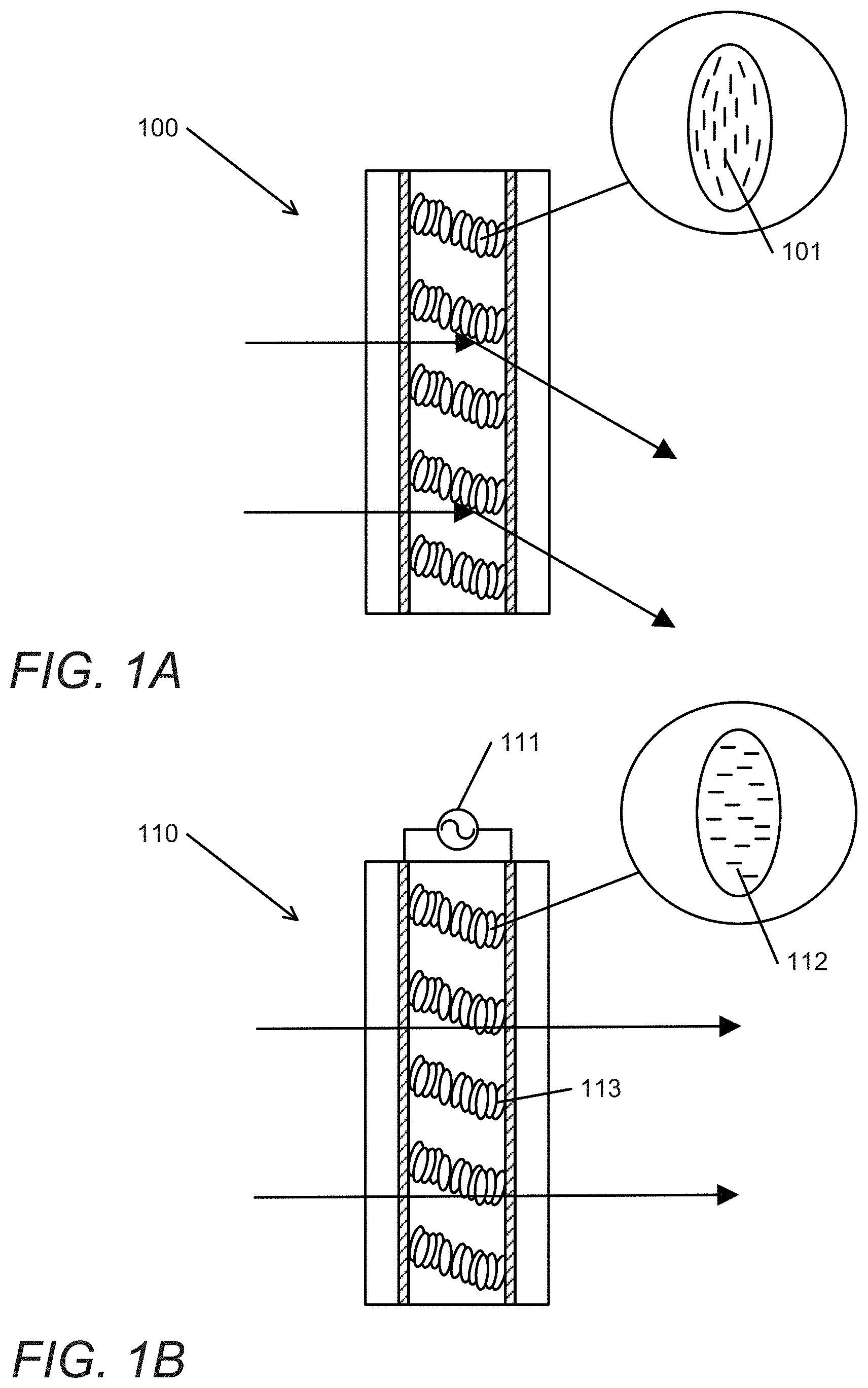
[0060] The resulting volume phase grating can exhibit very high diffraction efficiency, which can be controlled by the magnitude of the electric field applied across the film. When an electric field is applied to the grating via transparent electrodes, the natural orientation of the LC droplets can change, causing the refractive index modulation of the fringes to lower and the hologram diffraction efficiency to drop to very low levels. Typically, the electrodes are configured such that the applied electric field will be perpendicular to the substrates. In a number of embodiments, the electrodes are fabricated from indium tin oxide (ITO). In the OFF state with no electric field applied, the extraordinary axis of the liquid crystals generally aligns normal to the fringes. The grating thus exhibits high refractive index modulation and high diffraction efficiency for P-polarized light. When an electric field is applied to the HPDLC, the grating switches to the ON state wherein the extraordinary axes of the liquid crystal molecules align parallel to the applied field and hence perpendicular to the substrate. In the ON state, the grating exhibits lower refractive index modulation and lower diffraction efficiency for both S- and P-polarized light. Thus, the grating region no longer diffracts light. Each grating region can be divided into a multiplicity of grating elements such as for example a pixel matrix according to the function of the HPDLC device. Typically, the electrode on one substrate surface is uniform and continuous, while electrodes on the opposing substrate surface are patterned in accordance to the multiplicity of selectively switchable grating elements.
[0061] Typically, the SBG elements are switched clear in 30 .mu.s with a longer relaxation time to switch ON. The diffraction efficiency of the device can be adjusted, by means of the applied voltage, over a continuous range. In many cases, the device exhibits near 100% efficiency with no voltage applied and essentially zero efficiency with a sufficiently high voltage applied. In certain types of HPDLC devices, magnetic fields can be used to control the LC orientation. In some HPDLC applications, phase separation of the LC material from the polymer can be accomplished to such a degree that no discernible droplet structure results. An SBG can also be used as a passive grating. In this mode, its chief benefit is a uniquely high refractive index modulation. SBGs can be used to provide transmission or reflection gratings for free space applications. SBGs can be implemented as waveguide devices in which the HPDLC forms either the waveguide core or an evanescently coupled layer in proximity to the waveguide. The substrates used to form the HPDLC cell provide a total internal reflection (TIR) light guiding structure. Light can be coupled out of the SBG when the switchable grating diffracts the light at an angle beyond the TIR condition. In a number of embodiments, a reverse mode grating device can be implemented--i.e., the grating is in its non-diffracting (cleared) state when the applied voltage is zero and switches to its diffracting stated when a voltage is applied across the electrodes.
[0062] FIGS. 1A and 1B conceptually illustrate HPDLC SBG devices 100, 110 and the switching property of SBGs in accordance with various embodiments of the invention. In FIG. 1A, the SBG 100 is in an OFF state. As shown, the LC molecules 101 are aligned substantially normal to the fringe planes. As such, the SBG 100 exhibits high diffraction efficiency, and incident light can easily be diffracted. FIG. 1B illustrates the SBG 110 in an ON position. An applied voltage 111 can orient the optical axis of the LC molecules 112 within the droplets 113 to produce an effective refractive index that matches the polymer's refractive index, essentially creating a transparent cell where incident light is not diffracted. In the illustrative embodiment, an AC voltage source is shown. As can readily be appreciated, various voltage sources can be utilized depending on the specific requirements of a given application. Furthermore, different materials and device configurations can also be implemented. In some embodiments, the device implements different material systems and can operate in reverse with respect to the applied voltage--i.e., the device exhibits high diffraction efficiency in response to an applied voltage.
[0063] In some embodiments, LC can be extracted or evacuated from the SBG to provide a surface relief grating (SRG) that has properties very similar to a Bragg grating due to the depth of the SRG structure (which is much greater than that practically achievable using surface etching and other conventional processes commonly used to fabricate SRGs). The LC can be extracted using a variety of different methods, including but not limited to flushing with isopropyl alcohol and solvents. In many embodiments, one of the transparent substrates of the SBG is removed, and the LC is extracted. In further embodiments, the removed substrate is replaced. The SRG can be at least partially backfilled with a material of higher or lower refractive index. Such gratings offer scope for tailoring the efficiency, angular/spectral response, polarization, and other properties to suit various waveguide applications.
[0064] Waveguides in accordance with various embodiments of the invention can include various grating configurations designed for specific purposes and functions. In many embodiments, the waveguide is designed to implement a grating configuration capable of preserving eyebox size while reducing lens size by effectively expanding the exit pupil of a collimating optical system. The exit pupil can be defined as a virtual aperture where only the light rays which pass though this virtual aperture can enter the eyes of a user. In some embodiments, the waveguide includes an input grating optically coupled to a light source, a fold grating for providing a first direction beam expansion, and an output grating for providing beam expansion in a second direction, which is typically orthogonal to the first direction, and beam extraction towards the eyebox. As can readily be appreciated, the grating configuration implemented waveguide architectures can depend on the specific requirements of a given application. In some embodiments, the grating configuration includes multiple fold gratings. In several embodiments, the grating configuration includes an input grating and a second grating for performing beam expansion and beam extraction simultaneously. The second grating can include gratings of different prescriptions, for propagating different portions of the field-of-view, arranged in separate overlapping grating layers or multiplexed in a single grating layer. Multiplexed gratings can include the superimposition of at least two gratings having different grating prescriptions within the same volume. Gratings having different grating prescriptions can have different grating vectors and/or grating slant with respect to the waveguide's surface.
[0065] In several embodiments, the gratings within each layer are designed to have different spectral and/or angular responses. For example, in many embodiments, different gratings across different grating layers are overlapped, or multiplexed, to provide an increase in spectral bandwidth. In some embodiments, a full color waveguide is implemented using three grating layers, each designed to operate in a different spectral band (red, green, and blue). In other embodiments, a full color waveguide is implemented using two grating layers, a red-green grating layer and a green-blue grating layer. As can readily be appreciated, such techniques can be implemented similarly for increasing angular bandwidth operation of the waveguide. In addition to the multiplexing of gratings across different grating layers, multiple gratings can be multiplexed within a single grating layer--i.e., multiple gratings can be superimposed within the same volume. In several embodiments, the waveguide includes at least one grating layer having two or more grating prescriptions multiplexed in the same volume. In further embodiments, the waveguide includes two grating layers, each layer having two grating prescriptions multiplexed in the same volume. Multiplexing two or more grating prescriptions within the same volume can be achieved using various fabrication techniques. In a number of embodiments, a multiplexed master grating is utilized with an exposure configuration to form a multiplexed grating. In many embodiments, a multiplexed grating is fabricated by sequentially exposing an optical recording material layer with two or more configurations of exposure light, where each configuration is designed to form a grating prescription. In some embodiments, a multiplexed grating is fabricated by exposing an optical recording material layer by alternating between or among two or more configurations of exposure light, where each configuration is designed to form a grating prescription. As can readily be appreciated, various techniques, including those well known in the art, can be used as appropriate to fabricate multiplexed gratings.
[0066] In many embodiments, the waveguide can incorporate at least one of: angle multiplexed gratings, color multiplexed gratings, fold gratings, dual interaction gratings, rolled K-vector gratings, crossed fold gratings, tessellated gratings, chirped gratings, gratings with spatially varying refractive index modulation, gratings having spatially varying grating thickness, gratings having spatially varying average refractive index, gratings with spatially varying refractive index modulation tensors, and gratings having spatially varying average refractive index tensors. In some embodiments, the waveguide can incorporate at least one of: a half wave plate, a quarter wave plate, an anti-reflection coating, a beam splitting layer, an alignment layer, a photochromic back layer for glare reduction, and louvre films for glare reduction. In several embodiments, the waveguide can support gratings providing separate optical paths for different polarizations. In various embodiments, the waveguide can support gratings providing separate optical paths for different spectral bandwidths. In a number of embodiments, the gratings can be HPDLC gratings, switching gratings recorded in HPDLC (such switchable Bragg Gratings), Bragg gratings recorded in holographic photopolymer, or surface relief gratings. In many embodiments, the waveguide operates in a monochrome band. In some embodiments, the waveguide operates in the green band. In several embodiments, waveguide layers operating in different spectral bands such as red, green, and blue (RGB) can be stacked to provide a three-layer waveguiding structure. In further embodiments, the layers are stacked with air gaps between the waveguide layers. In various embodiments, the waveguide layers operate in broader bands such as blue-green and green-red to provide two-waveguide layer solutions. In other embodiments, the gratings are color multiplexed to reduce the number of grating layers. Various types of gratings can be implemented. In some embodiments, at least one grating in each layer is a switchable grating.
[0067] Waveguides incorporating optical structures such as those discussed above can be implemented in a variety of different applications, including but not limited to waveguide displays. In various embodiments, the waveguide display is implemented with an eyebox of greater than 10 mm with an eye relief greater than 25 mm. In some embodiments, the waveguide display includes a waveguide with a thickness between 2.0-5.0 mm. In many embodiments, the waveguide display can provide an image field-of-view of at least 50.degree. diagonal. In further embodiments, the waveguide display can provide an image field-of-view of at least 70.degree. diagonal. The waveguide display can employ many different types of picture generation units (PGUs). In several embodiments, the PGU can be a reflective or transmissive spatial light modulator such as a liquid crystal on Silicon (LCoS) panel or a micro electromechanical system (MEMS) panel. In a number of embodiments, the PGU can be an emissive device such as an organic light emitting diode (OLED) panel. In some embodiments, an OLED display can have a luminance greater than 4000 nits and a resolution of 4 k.times.4 k pixels. In several embodiments, the waveguide can have an optical efficiency greater than 10% such that a greater than 400 nit image luminance can be provided using an OLED display of luminance 4000 nits. Waveguides implementing P-diffracting gratings (i.e., gratings with high efficiency for P-polarized light) typically have a waveguide efficiency of 5%-6.2%. Since P-diffracting or S-diffracting gratings can waste half of the light from an unpolarized source such as an OLED panel, many embodiments are directed towards waveguides capable of providing both S-diffracting and P-diffracting gratings to allow for an increase in the efficiency of the waveguide by up to a factor of two. In some embodiments, the S-diffracting and P-diffracting gratings are implemented in separate overlapping grating layers. Alternatively, a single grating can, under certain conditions, provide high efficiency for both p-polarized and s-polarized light. In several embodiments, the waveguide includes Bragg-like gratings produced by extracting LC from HPDLC gratings, such as those described above, to enable high S and P diffraction efficiency over certain wavelength and angle ranges for suitably chosen values of grating thickness (typically, in the range 2-5 .mu.m).
Optical Recording Material Systems
[0068] HPDLC mixtures generally include LC, monomers, photoinitiator dyes, and coinitiators. The mixture (often referred to as syrup) frequently also includes a surfactant. For the purposes of describing the invention, a surfactant is defined as any chemical agent that lowers the surface tension of the total liquid mixture. The use of surfactants in PDLC mixtures is known and dates back to the earliest investigations of PDLCs. For example, a paper by R. L Sutherland et al., SPIE Vol. 2689, 158-169, 1996, the disclosure of which is incorporated herein by reference, describes a PDLC mixture including a monomer, photoinitiator, coinitiator, chain extender, and LCs to which a surfactant can be added. Surfactants are also mentioned in a paper by Natarajan et al, Journal of Nonlinear Optical Physics and Materials, Vol. 5 No. I 89-98, 1996, the disclosure of which is incorporated herein by reference. Furthermore, U.S. Pat. No. 7,018,563 by Sutherland; et al., discusses polymer-dispersed liquid crystal material for forming a polymer-dispersed liquid crystal optical element having: at least one acrylic acid monomer; at least one type of liquid crystal material; a photoinitiator dye; a coinitiator; and a surfactant. The disclosure of U.S. Pat. No. 7,018,563 is hereby incorporated by reference in its entirety.
[0069] The patent and scientific literature contains many examples of material systems and processes that can be used to fabricate SBGs, including investigations into formulating such material systems for achieving high diffraction efficiency, fast response time, low drive voltage, and so forth. U.S. Pat. No. 5,942,157 by Sutherland, and U.S. Pat. No. 5,751,452 by Tanaka et al. both describe monomer and liquid crystal material combinations suitable for fabricating SBG devices. Examples of recipes can also be found in papers dating back to the early 1990s. Many of these materials use acrylate monomers, including: [0070] R. L. Sutherland et al., Chem. Mater. 5, 1533 (1993), the disclosure of which is incorporated herein by reference, describes the use of acrylate polymers and surfactants. Specifically, the recipe includes a crosslinking multifunctional acrylate monomer; a chain extender N-vinyl pyrrolidinone, LC E7, photoinitiator rose Bengal, and coinitiator N-phenyl glycine. Surfactant octanoic acid was added in certain variants. [0071] Fontecchio et al., SID 00 Digest 774-776, 2000, the disclosure of which is incorporated herein by reference, describes a UV curable HPDLC for reflective display applications including a multi-functional acrylate monomer, LC, a photoinitiator, a coinitiators, and a chain terminator. [0072] Y. H. Cho, et al., Polymer International, 48, 1085-1090, 1999, the disclosure of which is incorporated herein by reference, discloses HPDLC recipes including acrylates. [0073] Karasawa et al., Japanese Journal of Applied Physics, Vol. 36, 6388-6392, 1997, the disclosure of which is incorporated herein by reference, describes acrylates of various functional orders. [0074] T. J. Bunning et al., Polymer Science: Part B: Polymer Physics, Vol. 35, 2825-2833, 1997, the disclosure of which is incorporated herein by reference, also describes multifunctional acrylate monomers. [0075] G. S. Iannacchione et al., Europhysics Letters Vol. 36 (6). 425-430, 1996, the disclosure of which is incorporated herein by reference, describes a PDLC mixture including a penta-acrylate monomer, LC, chain extender, coinitiators, and photoinitiator. Acrylates offer the benefits of fast kinetics, good mixing with other materials, and compatibility with film forming processes. Since acrylates are cross-linked, they tend to be mechanically robust and flexible. For example, urethane acrylates of functionality 2 (di) and 3 (tri) have been used extensively for HPDLC technology. Higher functionality materials such as penta and hex functional stems can also be used.
Modulation of Material Composition
[0076] High luminance and excellent color fidelity are important factors in various waveguide applications. In each case, high uniformity across the FOV can be desired. However, the fundamental optics of waveguides can lead to non-uniformities due to gaps or overlaps of beams bouncing down the waveguide. Further non-uniformities may arise from imperfections in the gratings and non-planarity of the waveguide substrates. In SBGs, there can exist a further issue of polarization rotation by birefringent gratings. In applicable cases, the biggest challenge is usually the fold grating where there are millions of light paths resulting from multiple intersections of the beam with the grating fringes. Careful management of grating properties, particularly the refractive index modulation, can be utilized to overcome non-uniformity.
[0077] Out of the multitude of possible beam interactions (diffraction or zero order transmission), only a subset contributes to the signal presented at the eye box. By reverse tracing from the eyebox, fold regions contributing to a given field point can be pinpointed. The precise correction to the modulation that is needed to send more into the dark regions of the output illumination can then be calculated. Having brought the output illumination uniformity for one color back on target, the procedure can be repeated for other colors. Once the index modulation pattern has been established, the design can be exported to the deposition mechanism, with each target index modulation translating to a unique deposition setting for each spatial resolution cell on the substrate to be coated/deposited. The resolution of the deposition mechanism can depend on the technical limitations of the system utilized. In many embodiments, the spatial pattern can be implemented to 30 micrometers resolution with full repeatability.
[0078] Compared with waveguides utilizing surface relief gratings (SRGs), SBG waveguides implementing manufacturing techniques in accordance with various embodiments of the invention can allow for the grating design parameters that impact efficiency and uniformity, such as but not limited to refractive index modulation and grating thickness, to be adjusted dynamically during the deposition process without the need for a different master. With SRGs where modulation is controlled by etch depth, such schemes would not be practical as each variation of the grating would entail repeating the complex and expensive tooling process. Additionally, achieving the required etch depth precision and resist imaging complexity can be very difficult.
[0079] Deposition processes in accordance with various embodiments of the invention can provide for the adjustment of grating design parameters by controlling the type of material that is to be deposited. Various embodiments of the invention can be configured to deposit different materials, or different material compositions, in different areas on the substrate. For example, deposition processes can be configured to deposit HPDLC material onto an area of a substrate that is meant to be a grating region and to deposit monomer onto an area of the substrate that is meant to be a non-grating region. In several embodiments, the deposition process is configured to deposit a layer of optical recording material that varies spatially in component composition, allowing for the modulation of various aspects of the deposited material. The deposition of material with different compositions can be implemented in several different ways. In many embodiments, more than one deposition head can be utilized to deposit different materials and mixtures. Each deposition head can be coupled to a different material/mixture reservoir. Such implementations can be used for a variety of applications. For example, different materials can be deposited for grating and non-grating areas of a waveguide cell. In some embodiments, HPDLC material is deposited onto the grating regions while only monomer is deposited onto the non-grating regions. In several embodiments, the deposition mechanism can be configured to deposit mixtures with different component compositions.
[0080] In some embodiments, spraying nozzles can be implemented to deposit multiple types of materials onto a single substrate. In waveguide applications, the spraying nozzles can be used to deposit different materials for grating and non-grating areas of the waveguide. In many embodiments, the spraying mechanism is configured for printing gratings in which at least one the material composition, birefringence, and/or thickness can be controlled using a deposition apparatus having at least two selectable spray heads. In some embodiments, the manufacturing system provides an apparatus for depositing grating recording material optimized for the control of laser banding. In several embodiments, the manufacturing system provides an apparatus for depositing grating recording material optimized for the control of polarization non-uniformity. In several embodiments, the manufacturing system provides an apparatus for depositing grating recording material optimized for the control of polarization non-uniformity in association with an alignment control layer. In a number of embodiments, the deposition workcell can be configured for the deposition of additional layers such as beam splitting coatings and environmental protection layers. Inkjet print heads can also be implemented to print different materials in different regions of the substrate.
[0081] As discussed above, deposition processes can be configured to deposit optical recording material that varies spatially in component composition. Modulation of material composition can be implemented in many different ways. In a number of embodiments, an inkjet print head can be configured to modulate material composition by utilizing the various inkjet nozzles within the print head. By altering the composition on a "dot-by-dot" basis, the layer of optical recording material can be deposited such that it has a varying composition across the planar surface of the layer. Such a system can be implemented using a variety of apparatuses including but not limited to inkjet print heads. Similar to how color systems use a palette of only a few colors to produce a spectrum of millions of discrete color values, such as the CMYK system in printers or the additive RGB system in display applications, inkjet print heads in accordance with various embodiments of the invention can be configured to print optical recording materials with varying compositions using only a few reservoirs of different materials. Different types of inkjet print heads can have different precision levels and can print with different resolutions. In many embodiments, a 300 DPI ("dots per inch") inkjet print head is utilized. Depending on the precision level, discretization of varying compositions of a given number of materials can be determined across a given area. For example, given two types of materials to be printed and an inkjet print head with a precision level of 300 DPI, there are 90,001 possible discrete values of composition ratios of the two types of materials across a square inch for a given volume of printed material if each dot location can contain either one of the two types of materials. In some embodiments, each dot location can contain either one of the two types of materials or both materials. In several embodiments, more than one inkjet print head is configured to print a layer of optical recording material with a spatially varying composition. Although the printing of dots in a two-material application is essentially a binary system, averaging the printed dots across an area can allow for discretization of a sliding scale of ratios of the two materials to be printed. For example, the amount of discrete levels of possible concentrations/ratios across a unit square is given by how many dot locations can be printed within the unit square. As such, there can be a range of different concentration combinations, ranging from 100% of the first material to 100% of the second material. As can readily be appreciated, the concepts are applicable to real units and can be determined by the precision level of the inkjet print head. Although specific examples of modulating the material composition of the printed layer are discussed, the concept of modulating material composition using inkjet print heads can be expanded to use more than two different material reservoirs and can vary in precision levels, which largely depends on the types of print heads used.
[0082] Varying the composition of the material printed can be advantageous for several reasons. For example, in many embodiments, varying the composition of the material during deposition can allow for the formation of a waveguide with gratings that have spatially varying diffraction efficiencies across different areas of the gratings. In embodiments utilizing HPDLC mixtures, this can be achieved by modulating the relative concentration of liquid crystals in the HPDLC mixture during the printing process, which creates compositions that can produce gratings with varying diffraction efficiencies when the material is exposed. In several embodiments, a first HPDLC mixture with a certain concentration of liquid crystals and a second HPDLC mixture that is liquid crystal-free are used as the printing palette in an inkjet print head for modulating the diffraction efficiencies of gratings that can be formed in the printed material. In such embodiments, discretization can be determined based on the precision of the inkjet print head. A discrete level can be given by the concentration/ratio of the materials printed across a certain area. In this example, the discrete levels range from no liquid crystal to the maximum concentration of liquid crystals in the first PDLC mixture.
[0083] The ability to vary the diffraction efficiency across a waveguide can be used for various purposes. A waveguide is typically designed to guide light internally by reflecting the light many times between the two planar surfaces of the waveguide. These multiple reflections can allow for the light path to interact with a grating multiple times. In many embodiments, a layer of material can be printed with varying composition of materials such that the gratings formed have spatially varying diffraction efficiencies to compensate for the loss of light during interactions with the gratings to allow for a uniform output intensity. For example, in some waveguide applications, an output grating is configured to provide exit pupil expansion in one direction while also coupling light out of the waveguide. The output grating can be designed such that when light within the waveguide interact with the grating, only a percentage of the light is refracted out of the waveguide. The remaining portion continues in the same light path, which remains within TIR and continues to be reflected within the waveguide. Upon a second interaction with the same output grating again, another portion of light is refracted out of the waveguide. During each refraction, the amount of light still traveling within the waveguide decreases by the amount refracted out of the waveguide. As such, the portions refracted at each interaction gradually decreases in terms of total intensity. By varying the diffraction efficiency of the grating such that it increases with propagation distance, the decrease in output intensity along each interaction can be compensated, allowing for a uniform output intensity.
[0084] Varying the diffraction efficiency can also be used to compensate for other attenuation of light within a waveguide. All objects have a degree of reflection and absorption. Light trapped in TIR within a waveguide are continually reflected between the two surfaces of the waveguide. Depending on the material that makes up the surfaces, portions of light can be absorbed by the material during each interaction. In many cases, this attenuation is small, but can be substantial across a large area where many reflections occur. In many embodiments, a waveguide cell can be printed with varying compositions such that the gratings formed from the optical recording material layer have varying diffraction efficiencies to compensate for the absorption of light from the substrates. Depending on the substrates, certain wavelengths can be more prone to absorption by the substrates. In a multi-layered waveguide design, each layer can be designed to couple in a certain range of wavelengths of light. Accordingly, the light coupled by these individual layers can be absorbed in different amounts by the substrates of the layers. For example, in a number of embodiments, the waveguide is made of a three-layered stack to implement a full color display, where each layer is designed for one of red, green, and blue. In such embodiments, gratings within each of the waveguide layers can be formed to have varying diffraction efficiencies to perform color balance optimization by compensating for color imbalance due to loss of transmission of certain wavelengths of light.
In addition to varying the liquid crystal concentration within the material in order to vary the diffraction efficiency, another technique includes varying the thickness of the waveguide cell. This can be accomplished through the use of spacers. In many embodiments, spacers are dispersed throughout the optical recording material for structural support during the construction of the waveguide cell. In some embodiments, different sizes of spacers are dispersed throughout the optical recording material. The spacers can be dispersed in ascending order of sizes across one direction of the layer of optical recording material. When the waveguide cell is constructed through lamination, the substrates sandwich the optical recording material and, with structural support from the varying sizes of spacers, create a wedge-shaped layer of optical recording material. spacers of varying sizes can be dispersed similar to the modulation process described above. Additionally, modulating spacer sizes can be combined with modulation of material compositions. In several embodiments, reservoirs of HPDLC materials each suspended with spacers of different sizes are used to print a layer of HPDLC material with spacers of varying sizes strategically dispersed to form a wedge-shaped waveguide cell. In a number of embodiments, spacer size modulation is combined with material composition modulation by providing a number of reservoirs equal to the product of the number of different sizes of spacers and the number of different materials used. For example, in one embodiment, the inkjet print head is configured to print varying concentrations of liquid crystal with two different spacer sizes. In such an embodiment, four reservoirs can be prepared: a liquid crystal-free mixture suspension with spacers of a first size, a liquid crystal-free mixture-suspension with spacers of a second size, a liquid crystal-rich mixture-suspension with spacers of a first size, and a liquid crystal-rich mixture-suspension with spacers of a second size. Further discussion regarding material modulation can be found in U.S. application Ser. No. 16/203,071 filed Nov. 18, 2018 entitled "Systems and Methods for Manufacturing Waveguide Cells." The disclosure of U.S. application Ser. No. 16/203,491 is hereby incorporated by reference in its entirety for all purposes.
Waveguide Backlights
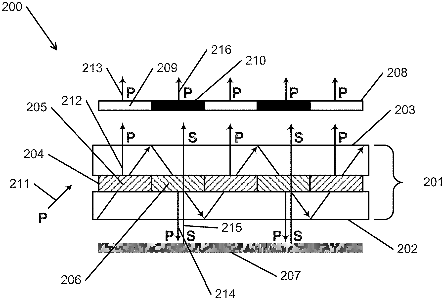
[0085] Waveguide backlights in accordance with various embodiments of the invention can be implemented using a variety of different configurations. As can readily be appreciated, the specific configuration implemented can depend on various factors, including but not limited to the intended application, cost constraints, form factor constraints, etc. In many embodiments, the waveguide backlight is implemented with at least one waveguide layer containing at least one grating layer sandwiched by first and second substrates. The substrates can include various transparent materials, including but not limited to glass and plastics. The grating layer(s) can include different sets of grating elements configured for various purposes. In some embodiments, the grating layer includes two different sets of grating elements, each set configured and designed to have high diffraction efficiency for a specific wavelength band and/or angular band. In a number of embodiments, the grating layer includes two different sets of grating elements, where each set contains grating elements having the same K-vectors. In various embodiments, the two sets of grating elements have opposing K-vectors. In several embodiments, the grating layer includes two different sets of grating elements, each set configured and designed to diffract and extract light from different directions. For example, in a number of embodiments, the grating layer includes a first set of grating elements configured to diffract TIR light that is reflected off the first substrate and to extract such light through the second substrate and a second set of grating elements configured to diffract TIR light that is reflected off the second substrate and to extract such light through the first substrate.
[0086] The grating elements implemented in waveguide backlights can be arranged in a number of different configurations. In many embodiments, the waveguide backlight includes a grating layer having first and second sets of grating elements that are interspersed with one another. In some embodiments, the first and second set of grating elements are disposed across two different grating layers. The two different grating layers can be disposed adjacent one another (i.e., the waveguide layer includes two grating layers sandwiched between two substrates) or across two different waveguide layers. As can readily be appreciated, such grating architectures can be expanded to implement more than two sets of grating elements. Furthermore, the waveguide layer(s) can be configured to implement a variety of different grating structures, including but not limited to HPDLC gratings, switching gratings recorded in HPDLC (such switchable Bragg Gratings), Bragg gratings recorded in holographic photopolymer, evacuated Bragg gratings, backfilled evacuated Bragg gratings, and surface relief gratings.
[0087] Depending on the type of gratings implemented, light polarization responses can be a large factor in how and how well the waveguide backlight operates. For example, in some embodiments, the gratings are implemented using an HPDLC material that forms gratings that are sensitive to P-polarized light. In such cases, the waveguide backlight can be designed with the appropriate considerations. The waveguide backlight can include various waveplate and retarder configurations for manipulating the polarization of light traveling throughout the waveguide backlight. In some embodiments, the waveguide backlight includes a quarter-wave plate (QWP). A QWP converts linearly polarized light into circularly polarized light and vice versa. In further embodiments, the QWP is implemented with a mirror, which can be formed on an outer surface of the QWP. Such configurations can allow for incident linearly polarized light to be reflected with its polarization orthogonally changed. For example, an incident P-polarized light ray can be converted into circularly polarized light by the QWP, reflected by the mirror to give circularly polarized light in an opposing direction, and finally converted into linearly S-polarized light. In many embodiments, the waveguide backlight includes a half-wave plate (HWP) for switching the polarization of P-polarized light into S-polarized light and vice versa. In a number of embodiments, the waveguide backlight includes a substrate supporting half wave retarders. Various types of light sources can be utilized to introduce light into the backlight. In a number of embodiments, P- and/or S-polarized light is coupled into the waveguide backlight. In several embodiments, unpolarized light is coupled into the waveguide backlight. As can readily be appreciated, the specific configuration of input light and grating structures can depend on the specific requirements of a given application.
[0088] Grating elements within a waveguide backlight can be arranged and implemented in various configurations. In several embodiments, all of the grating elements in a waveguide layer are designed to operate at a common wavelength band. As described above, the grating elements can have K-vectors configured to diffract upward-going or downward-going rays in a waveguide layer. In several embodiments, both types of gratings are provided in a waveguide layer. In further embodiments, both types of gratings are provided in a single grating layer. In some embodiments, the grating elements can have K-vectors in differing directions but operating at a common wavelength band. It should be appreciated from the discussions that any number of separate wavelength bands can be provided. FIG. 2 conceptually illustrates a waveguide backlight having two sets of interspersed grating elements in accordance with an embodiment of the invention. As shown, the waveguide backlight 200 includes: a waveguide 201 formed by substrates 202,203 sandwiching a grating layer 204. In many embodiments, a source of light (which is not illustrated) can be optically coupled to the waveguide structure 201 and can be configured to emit collimated light. The substrates 202,203 can provide a TIR structure for the input light. The grating layer 204 can include a plurality of grating elements for diffracting light out of the waveguide and, ultimately, towards an external illumination surface. In the illustrative embodiment, the grating layer 204 includes two sets of plane gratings having two grating configurations (e.g., grating elements 205,206) with opposing K-vectors for diffracting TIR light coming from different directions. For example, grating element 205 is configured to diffract light reflected from the outer surface of substrate 202 while grating element 206 is configured to diffract light reflected from the outer surface of substrate 203. For ease of clarity, the two different directions of light can also be referred to as upward- and downward-going TIR light, respectively, with the orientation of the waveguide in the figure as a frame of reference. The pair of grating configurations are repeated along the grating layer 204 in the embodiment of FIG. 2 to form two sets of interspersed grating elements.
[0089] The waveguide backlight 200 of FIG. 2 further includes a quarter wave plate 207 and a transparent layer 208 divided into clear regions 209 and regions supporting half wave retarders 210. In the illustrative embodiment, the QWP 207 is implemented along with a mirror to provide reflection of incident light while changing its polarization orthogonally. The QWP 207 and the transparent layer 208 can be separated from the waveguide 201 by air gaps or layers of low refractive index material, including but not limited to a nanoporous material. Methods of such implementations are discussed in the sections above. Referring back to FIG. 2, the illustrative embodiment shows operation of the waveguide backlight 200 where input P-polarized light 211 (which is the preferred light polarization state for diffraction by SBGs) undergoes TIR within the waveguide 201. A portion of this light (upward-going TIR light) can be diffracted (212) by grating element 205 and directed towards a clear region 209 of the transparent layer 208 to provide P-polarized output light 213. Downward-going TIR light incident on the grating element 206 can be diffracted (214) downwards and reflected (215) by the QWP 207 with its polarization rotated from P to S. The S-polarized light can travel through the grating layer 204 and proceed out of the waveguide 201 towards a half wave retarder region 210 of the transparent layer 208. After transmission through a half wave retarder region 210, the light has its polarization rotated from S to P (216). By repeating the above ray-grating interactions across the waveguide, extraction of the incident light towards a similar direction can be accomplished to a high degree. As can readily be appreciated, such configurations can include various modifications, which can depend on the specific requirements of a given application. For example, in several embodiments, the diffraction efficiencies of the grating elements can be varied along the waveguide path to control uniformity. In many embodiments, the grating elements can be electrically switchable. In some embodiments, a grating layer can be formed between transparent substrates with transparent conductive coatings applied to each substrate. At least one of the coatings can be patterned into independently addressable elements overlapping the grating elements. An electrical control circuit operative to apply voltages across each of the grating elements can be provided.
[0090] FIG. 3 conceptually illustrates a flow chart of a process for providing a waveguide backlight in accordance with an embodiment of the invention. As shown, the process 300 includes providing (301) a waveguide having a first set of grating elements for diffracting downward-going rays and a second set of grating elements diffracting upward-going rays, wherein the grating elements are disposed between first and second transparent substrates. Input light can be coupled (302) into a total internal reflection path within the waveguide. Various types of input light can be utilized. In many embodiments, narrow band laser illumination is utilized. In some embodiments, the input light is P-polarized light. A portion of the input light can be extracted (303) through an outer surface of the first transparent substrate using the first set of grating elements, and a portion of the input light can be extracted (304) through an outer surface of the second transparent substrate using the second set of grating elements. In many embodiments, the first set of grating elements is configured to extract light reflected from the outer surface of the second substrate, and the second set of grating elements is configured to extract light reflected from the outer surface of the first substrate. Various types of gratings can be implemented. In several embodiments, P-polarization sensitive gratings are utilized. In a number of embodiments, S-polarization sensitive gratings are utilized. In some embodiments, both types of gratings are implemented. As can readily be appreciated, the types of gratings utilized can depend on the type of input light. The light extracted from the second transparent surface can have its polarization rotated (305) and can be reflected towards the waveguide, propagating through to the outer surface of the first transparent surface. In many embodiments, a QWP is utilized to rotate the polarization of the light and to reflect it towards the waveguide. The light with its polarization rotated can optionally have its polarization rotated (306) again after its propagation through the outer surface of the first transparent substrate. In some embodiments, a substrate containing HWP regions can be implemented to rotate the polarization of the light after its propagation through the first transparent substrate. Although FIG. 3 illustrates a specific method of providing a waveguide backlight, various other processes can be implemented as appropriate depending on the specific requirements of a given application. For example, in some embodiments, the input light contains only P-polarized light. In other embodiments, the input light contains both S- and P-polarized light.
[0091] Waveguide backlights in accordance with various embodiments of the invention can be configured for many different applications. In many embodiments, the waveguide backlight is configured for narrow band illumination applications--i.e., the wavelength band can have a narrow bandwidth as is typically provided by a laser. In some embodiments, the wavelength band can have a broader bandwidth such as can be provided by an LED. As can readily be appreciated, the backlight can also be used to provide non-visible radiation such as infrared and ultraviolet. In some embodiments, the waveguide backlight is configured as a color waveguide backlight. Such backlights can be implemented based on principles similar to those shown in FIG. 2. In some embodiments, the backlight provides light from red, green, and blue (RGB) sources. In such embodiments, the backlight can include RGB grating elements interspersed within a single layer or disposed in some way over two or more layers. In some embodiments, separate RGB layers can be used. In several embodiments, the waveguide backlight operates using first and second wavelength input light that covers a large portion of the visible band. For example, in various embodiments, the first wavelength light covers the blue to green band, and the second wavelength light can cover the green to red band. In several embodiments, a color waveguide backlight can be implemented utilizing separate grating layers for each color component to be emitted from the backlight. In some embodiments, the waveguide backlight incorporates SBGs. In such cases, the waveguide backlight can include a first set of grating elements configured to switch into a diffracting state when the light source emits light of a first wavelength band and a second set of grating elements configured to switch into a diffracting state when the source emits light of a second wavelength band.
[0092] FIG. 4 conceptually illustrates a waveguide backlight with two waveguide layers in accordance with an embodiment of the invention. In the following paragraphs, to simplify the description of the invention, the discussions will include waveguides for emitting light in two different wavelength bands (first and second wavelength light) using first and second sets of grating elements formed in two waveguide layers, each waveguide layer containing a single grating layer. However, any number of waveguides layers and grating layers can be utilized as appropriated depending on the specific requirements of a given application. Referring back to FIG. 2A, the waveguide backlight 400 shown includes first and second waveguides 401,402. The backlight 400 further includes a quarter wave plate (QWP) 403 and a transparent substrate 404 divided into clear regions 405 and regions supporting half wave retarders 406. Each waveguide can be configured to operate according to principles similar to those shown in FIG. 2. For example, the first waveguide 401 can be configured to receive p-polarized light of a first wavelength band, and the second waveguide 402 can be configured to receive p-polarized light of a second wavelength band. In the illustrative embodiment, each of the first and second waveguides 401,402 includes a grating layer 407,408. The second waveguide 402 can include a similar configuration of grating elements to that of the first waveguide 401 but operating in a different wavelength band. For example, in the illustrative embodiment, the first waveguide 401 can include grating elements configured to operate in the red-green wavelength band while the second waveguide 402 can include grating elements configured to operate in the green-blue wavelength band, allowing for the implementation of a full color waveguide backlight. In other embodiments, a full color waveguide backlight can be implemented with three waveguide layers, each configured to operate in one of red, green, and blue wavelength band. As indicated by the two sets of rays (dashed and solid, representing rays of different wavelength light), it is shown that the ray and grating interactions of the second waveguide 402 are similar to those of the first waveguide 401. The first and second wavelength light extracted from the two waveguides can be combined to provide uniform illumination. In many embodiments, the first and second wavelength light can be introduced to the waveguides sequentially.
[0093] The waveguide structure of FIG. 4 can be equivalently implemented using a variety of different grating configurations. In some embodiments, the backlight can be implemented as a single waveguide layer containing pluralities of grating elements configured for operation at different wavelength bands. FIG. 5 conceptually illustrates a waveguide backlight with a single waveguide layer in accordance with an embodiment of the invention. As shown, the waveguide backlight 500 includes a grating configuration 501 formed of two adjacent grating layers 502,503 sandwiched by two substrates 504,505. The waveguide backlight 500 further includes a QWP 506 and a transparent substrate 507 divided into clear regions 508 and regions supporting half wave retarders 509. In the illustrative embodiment, the grating configuration 501 includes two grating layers 508,509 capable of operating in a different wavelength band. In many embodiments, the operating wavelength band of the two grating layers covers a large portion of the visible band. Each grating layer further includes two interspersed sets of grating elements 510,511 and 512,513 for diffracting upward- (510,512) and downward-going (511,513) TIR light. As can readily be appreciated, the backlight shown in FIG. 5 can operate in accordance with principles similar to those shown in FIG. 4. In FIG. 5, the two grating layers are shown in separate adjacent layers, the combination of which provides the grating configuration. In other embodiments, the grating elements across the two grating layers are multiplexed and superimposed into a single layer. For example, grating elements 510 can be multiplexed with grating elements 512, and grating elements A 311 can be multiplexed with grating elements 513.
[0094] Although FIGS. 4 and 5 illustrate specific polychromatic waveguide backlight implementations, various configurations can be implemented as appropriate depending on the specific requirements of a given application. For example, in several embodiments, the waveguide backlight includes two waveguide layers, each containing interspersed grating elements configured to operate in two wavelength bands. FIG. 6 conceptually illustrates a waveguide backlight 600 having two waveguide layers 601,602 each containing a grating layer 603,604 with alternating first wavelength-diffracting 605 and second wavelength-diffracting 606 grating elements in accordance with an embodiment of the invention. The grating elements 605,606 can all have K-vectors configured to diffract one of upward-going or downward-going TIR light through an outer surface (e.g., upward-going in the illustrative embodiment of FIG. 6) of the waveguide. In the illustrative embodiment, the first wavelength-diffracting and second wavelength-diffracting grating elements 605,606 are spatially overlapped. During operation, first wavelength P-polarized light 607 and second wavelength P-polarized light 608 can be coupled into the waveguides and undergo diffraction and extraction as indicated by rays 609,610 corresponding to first wavelength light and rays 611,612 corresponding to second wavelength light. The waveguide structure of FIG. 6 can be equivalently implemented using a variety of different grating configurations. Similar to the embodiment shown in FIG. 5, the backlight shown in FIG. 6 can be implemented with a single waveguide layer. FIG. 7 conceptually illustrates a waveguide backlight having a single waveguide layer with alternating wavelength-diffracting grating elements in accordance with an embodiment of the invention. As shown, the waveguide backlight 700 includes a single grating configuration 701 sandwiched by two substrates 702,703. The grating configuration 701 includes two grating layers 704,705. In the illustrative embodiment, two sets of grating elements 706,707 are interspersed within and across both grating layers 704,705. Grating elements from the first set 706 spatially overlap grating elements from the second set 707. The grating elements can be configured in a variety of different ways. In some embodiments, each set of grating elements are configured to diffract a specific wavelength band. In many embodiments, all of the grating vectors are configured to have similar K-vectors. In the embodiment of FIG. 7, all of the grating elements are configured with diffract and direct light towards the same direction. As can readily be appreciated, the waveguide backlight shown in FIG. 7 can operate in accordance with principles similar to those shown in FIG. 6. In FIG. 7, the two grating layers 704,705 are shown in separate adjacent layers, the combination of which provides the single grating configuration 701. In other embodiments, the grating elements within the two grating layers 704,705 are multiplexed and superimposed in the same layer--i.e., each multiplexed region contains grating element 706 and grating element 707.
[0095] Although FIGS. 2-7 illustrate specific waveguide backlights receiving P-polarized input light, waveguide backlights in accordance with various embodiments of the invention can be configured for operation with various light sources. FIG. 8 conceptually illustrates a waveguide backlight 800 having two waveguide layers 801,802 with alternating wavelength-diffracting grating elements for input light having orthogonal polarizations in accordance with an embodiment of the invention. As shown, the first waveguide layer 801 includes a first grating layer 803 with a first set of alternating first wavelength-diffracting 804 and second wavelength-diffracting 805 grating elements. Similarly, the second waveguide layer 802 includes a second grating layer 806 with a second set of alternating first wavelength-diffracting 804 and second wavelength-diffracting 805 grating elements. The waveguide backlight 800 further includes a QWP 807. Various light sources can be implemented as appropriate with such configurations. In the illustrative embodiment, the input light includes first and second wavelength light 808,809 having orthogonal polarizations. For example, the input first wavelength light 808 can be P-polarized and the input second wavelength light 809 can be S-polarized. In the illustrative embodiment, the first wavelength-diffracting grating elements 804 have K-vectors configured to diffract upward-going TIR light through the upper waveguide surface 810 of the first waveguide layer 801, and the second wavelength-diffracting grating elements 805 have K-vectors configured to diffract downward-going TIR light through the lower waveguide surface 811 of the second waveguide layer 802. As shown, the first wavelength-diffracting and second wavelength-diffracting grating elements 804,805 are spatially overlapped. The light (second wavelength light) extracted from the lower waveguide surface 813 has its polarization rotated from S to P by the QWP 807 before being retransmitted through the two waveguide layers 801,802 and out of the upper surface 810. Hence, the output light from the waveguide backlight 800 is all P-polarized. Similar to the embodiments shown in FIGS. 5 and 7, the configuration shown in FIG. 8 can be implemented within a single waveguide layer. FIG. 9 conceptually illustrates a waveguide backlight implementation 900 of the embodiment of FIG. 8 using a single waveguide layer 901 with adjacent grating layers 902,903. As can readily be appreciated, such a waveguide backlight can operate according to principles similar to those shown in FIG. 8. Furthermore, such grating layers can also be implemented as a single layer containing multiplexed gratings.
[0096] An important principle underlying the embodiments discussed above is that Bragg gratings diffract with high efficiency when light satisfies the Bragg equation to within angular and wavelength tolerances set by the angular and spectral bandwidths of the grating. The spectral and angular bandwidths can be computed using theory of volume holographic gratings. Waveguided rays falling within the above bandwidth limits are referred to as being on-Bragg while rays falling outside the bandwidth are referred to as off-Bragg.
[0097] Another factor to be addressed in displays and illumination devices, particularly those using lasers, results from beam edge mismatching as a beam undergoes TIR. For a waveguide of thickness D, distance between successive beam-surface interactions W, and a TIR angle U, the condition for seamless matching of upward and downward going TIR beams is given by the equation 2D tan(U)=W. When this condition is not met, gaps or overlaps between adjacent beam portions can occur, which result in a non-uniformity in the output illumination called banding. Banding can be alleviated to some extent by using broadband sources such as LEDs. However, the effect can be much more difficult to overcome with lasers. In many embodiments, the waveguide backlight can be configured to operate entirely in collimated space. In other words, the input light and the output beams replicated at each beam grating interaction are all collimated. In some embodiments, the input beam is scanned in at least one angular direction. In several embodiments, the cross section of the input beam can be varied with incidence angle to match a debanding condition according to the embodiments or teaching disclosed in PCT/US2018/015553 "WAVEGUIDE DEVICE WITH UNIFORM OUTPUT ILLUMINATION", the disclosure of which is incorporated herein by reference in its entirety. In a number of embodiments, the input beam cross section can be adjusted by means of edges formed on a surface or layer supported by the waveguide as discussed in the above references.
[0098] In many embodiments, light is coupled into the waveguide using a grating or a prism. In many embodiments, the optics for coupling light into the waveguides may further include, beam splitters, filters, dichroic filters, polarization components, light integrators, condenser lenses, micro lenses, beam shaping elements and other components commonly used in display illumination systems.
[0099] In many embodiments, the light source is a laser scanned in at least one angular direction using an electromechanical beam deflector. In some embodiments, the laser scanner may be an electro optical device.
[0100] In many embodiments, light can be extracted from the waveguide into output paths that are angularly separated. In many embodiments that output paths can be substantially normal to a total internal reflection surface of the waveguide. In many embodiments, the light extracted from the waveguide is collimated.
[0101] In many embodiments, a grating element includes at least one selected from the group of a planar grating, a grating with optical power, a grating providing optical retardation, and a grating with diffusing properties. In many embodiments, the grating elements can have spatially varying diffraction efficiencies to enable extraction of light along the waveguide. In many embodiments, the grating elements have diffraction efficiencies proportional to voltages applied across the electrodes. In some embodiments, the grating elements can have phase retardations proportional to voltages applied across said electrodes. In many embodiments, the grating elements can be configured as a one-dimensional array of elongate elements. In many embodiments, the gratings can be configured as two-dimensional arrays. In many embodiments, the gratings elements are recorded in a Holographic Polymer Dispersed Liquid Crystal. In many embodiments the spatio-temporal addressing of grating elements by an electrical control circuit addresses can be characterized by a cyclic process. In many embodiments, the spatio-temporal addressing of grating elements by an electrical control circuit can be characterized by a random process.
DOCTRINE OF EQUIVALENTS
[0102] While the above description contains many specific embodiments of the invention, these should not be construed as limitations on the scope of the invention, but rather as an example of one embodiment thereof. It is therefore to be understood that the present invention may be practiced in ways other than specifically described, without departing from the scope and spirit of the present invention. Thus, embodiments of the present invention should be considered in all respects as illustrative and not restrictive. Accordingly, the scope of the invention should be determined not by the embodiments illustrated, but by the appended claims and their equivalents.
* * * * *
D00000
D00001
D00002
D00003
D00004
D00005
D00006
D00007
D00008
D00009
XML
uspto.report is an independent third-party trademark research tool that is not affiliated, endorsed, or sponsored by the United States Patent and Trademark Office (USPTO) or any other governmental organization. The information provided by uspto.report is based on publicly available data at the time of writing and is intended for informational purposes only.
While we strive to provide accurate and up-to-date information, we do not guarantee the accuracy, completeness, reliability, or suitability of the information displayed on this site. The use of this site is at your own risk. Any reliance you place on such information is therefore strictly at your own risk.
All official trademark data, including owner information, should be verified by visiting the official USPTO website at www.uspto.gov. This site is not intended to replace professional legal advice and should not be used as a substitute for consulting with a legal professional who is knowledgeable about trademark law.