High Data Rate Integrated Circuit With Transmitter Configuration
Fife; Keith G. ; et al.
U.S. patent application number 16/808276 was filed with the patent office on 2020-09-10 for high data rate integrated circuit with transmitter configuration. The applicant listed for this patent is LIFE TECHNOLOGIES CORPORATION. Invention is credited to Keith G. Fife, Jungwook Yang.
| Application Number | 20200284754 16/808276 |
| Document ID | / |
| Family ID | 1000004853380 |
| Filed Date | 2020-09-10 |


View All Diagrams
| United States Patent Application | 20200284754 |
| Kind Code | A1 |
| Fife; Keith G. ; et al. | September 10, 2020 |
HIGH DATA RATE INTEGRATED CIRCUIT WITH TRANSMITTER CONFIGURATION
Abstract
A high data rate integrated circuit, such as an integrated circuit including a large sensor array, may be implemented using clock multipliers in individual power domains, coupled to sets of transmitters, including a transmitter pair configuration. Reference clock distribution circuitry on the integrated circuit distributes a relatively low speed reference clock. In a transmitter pair configuration, each pair comprises a first transmitter and a second transmitter in a transmitter power domain. Also, each pair of transmitters includes a clock multiplier connected to the reference clock distribution circuitry, and disposed between the first and second transmitters, which produces a local transmit clock.
| Inventors: | Fife; Keith G.; (Palo Alto, CA) ; Yang; Jungwook; (Waban, MA) | ||||||||||
| Applicant: |
|
||||||||||
|---|---|---|---|---|---|---|---|---|---|---|---|
| Family ID: | 1000004853380 | ||||||||||
| Appl. No.: | 16/808276 | ||||||||||
| Filed: | March 3, 2020 |
Related U.S. Patent Documents
| Application Number | Filing Date | Patent Number | ||
|---|---|---|---|---|
| 14971173 | Dec 16, 2015 | 10605767 | ||
| 16808276 | ||||
| 62093548 | Dec 18, 2014 | |||
| Current U.S. Class: | 1/1 |
| Current CPC Class: | G01N 27/4148 20130101; G06F 30/392 20200101; G06F 30/394 20200101; G01N 27/4145 20130101 |
| International Class: | G01N 27/414 20060101 G01N027/414; G06F 30/392 20060101 G06F030/392; G06F 30/394 20060101 G06F030/394 |
Claims
1. An integrated circuit, comprising: a substrate; a data source on the substrate; peripheral circuitry on the substrate coupled to the data source to produce a stream of digital data; a clock multiplier on the substrate for producing a transmit clock, the transmit clock being disposed in an individual power domain on the substrate; and a transmitter on the substrate configured to receive a stream of data from the data source, the transmitter being connected to transmit the stream of data on an output pad using the transmit clock, the transmitter being disposed in a transmitter power domain on the substrate separate from the individual power domain of the clock multiplier.
2. The integrated circuit of claim 1, wherein the data source and the peripheral circuitry are disposed in a power domain or power domains separate from the individual power domain.
3. The integrated circuit of claim 1, including a plurality of transmitters on the substrate connected to the clock multiplier.
4. The integrated circuit of claim 1, including: a plurality of clock multipliers on the substrate for producing respective local transmit clocks, including a first clock multiplier of the plurality, the clock multipliers in the plurality being disposed in an individual power domains on the substrate; and a plurality of transmitters on the substrate, including a first transmitter of the plurality, the plurality of transmitters being arranged in sets having one or more members, and wherein each set is connected to one clock multiplier in the plurality of the clock multipliers.
Description
CROSS-REFERENCE TO RELATED APPLICATIONS
[0001] This application is a divisional application of U.S. patent application Ser. No. 14/971,173, which claims priority to U.S. Provisional Application No. 62/093,548 filed Dec. 18, 2014. Each application identified in this section are incorporated by reference herein, each in its entirety.
BACKGROUND
Field of the Invention
[0002] This disclosure, in general, relates to integrated circuit sensors operating at high data rates, such as used in DNA sequencing technologies, and configurations of transmitters on integrated circuits to support such data rates.
Description of Related Art
[0003] A variety of types of sensors have been used in the detection of chemical and/or biological processes. One type is a chemically-sensitive field effect transistor (chemFET). A chemFET includes a gate, a source, a drain separated by a channel region, and a sensitive area, such as a surface on the gate adapted for contact with a fluid, coupled to the channel region. The operation of the chemFET is based on the modulation of channel conductance caused by changes, such as changes in voltage, at the sensitive area which can be due to a chemical and/or biological reaction occurring in the fluid, for example. The modulation of the channel conductance can be sensed to detect and/or determine characteristics of the chemical and/or biological reaction that cause changes at the sensitive area. One way to measure the channel conductance is to apply appropriate bias voltages to the source and drain, and measure a resulting current flowing through the chemFET. A method of measuring channel conductance can include driving a known current through the chemFET and measuring a resulting voltage at the source or drain.
[0004] An ion-sensitive field effect transistor (ISFET) is a type of chemFET that includes an ion-sensitive layer at the sensitive area. The presence of ions in a fluid containing an analyte alters the surface potential at the interface between the ion-sensitive layer and the analyte fluid which can be due to the protonation or deprotonation of surface charge groups caused by the ions present in the fluid (i.e. an analyte solution). The change in surface potential at the sensitive area of the ISFET affects the gate voltage of the device, and thereby channel conductance, which change can be measured to indicate the presence and/or concentration of ions within the solution. Arrays of ISFETs can be used for monitoring chemical and/or biological reactions, such as DNA sequencing reactions based on the detection of ions present, generated, or used during the reactions. (See, for example, U.S. Pat. No. 7,948,015 to Rothberg et al., filed Dec. 14, 2007, which is incorporated by reference herein in its entirety.) More generally, large arrays of chemFETs or other types of sensors and detectors can be employed to detect and measure static and/or dynamic amounts or concentrations of a variety of analytes in a variety of processes. For example, the processes can be chemical and/or biological reactions, cell or tissue cultures or monitoring neural activity, nucleic acid sequencing, etc.
[0005] Many transmitters for high-speed links to connect with a reader capable of receiving the data can be used to provide high data rates sourced from a single sensor chip comprising large arrays of chemFETs using. However, difficulties can arise in implementation of large numbers of transmitters on a single chip, so that data integrity may be compromised or the data rates desired are not achieved. It may be desirable to provide a technology supporting very high data rates for use in integrated circuits comprising large high-speed data sources, such as the ISFET arrays and other sensor technologies used in DNA sequencing.
SUMMARY
[0006] Technology is described herein which can improve the integrity of data transmission from a device that includes a data source on a substrate that produces data at high data rate, such as a large array of ISFETs in a DNA sequencing sensor chip.
[0007] To support high data rate in one aspect of the technology described, a plurality of transmitters may be disposed in pairs around the substrate, and configured to receive streams of data from the data source in parallel. The transmitters in the plurality of transmitters are configured to transmit the corresponding streams of data on respective output pads using a corresponding local transmit clock. The local transmit clocks are produced using a plurality of clock multipliers, such as phase locked loops, placed on the substrate and linked across short distances to the corresponding pair of transmitters adjacent to the clock multiplier. A reference clock distribution circuit may be disposed on the substrate, to distribute a reference clock having a reference frequency to the plurality of clock multipliers. Clock multipliers in the plurality provide the corresponding local transmit clocks with a transmit clock frequency that may be a multiple of the reference clock frequency.
[0008] The clock multipliers can comprise phase locked loops with low pass filters, configured to reject jitter in the reference clock. In one example, the plurality of transmitters includes at least 20 transmitters capable of transmission at data rates greater than 1 Gb per second, and such transmitters are configured in at least 10 pairs. In another example, an integrated circuit includes 24 transmitters capable of transmission of data rates greater than 5 Gb per second, for a total throughput of 120 Gb per second or higher.
[0009] In another aspect of the technology described herein, an integrated circuit employing the plurality of transmitters can comprise a plurality of power domains. A clock multiplier on the integrated circuit may be deployed in a power domain that may be separate from the transmitter to which it is coupled. The transmitter may be deployed in a power domain separate from the data source on the integrated circuit. In embodiments in which the data source includes an array of analog sensors, such as ISFETs, the data source can include an analog power domain and a digital power domain. Thus, one aspect of the technology described herein includes a clock multiplier in an individual power domain on an integrated circuit having a clock signal line connected to one or more transmitters in a power domain, or power domains, separate from that of the clock multiplier. As described above, in one embodiment, the integrated circuit includes a plurality of pairs of transmitters with one clock multiplier per pair. In other embodiments, one clock multiplier in an individual power domain may provide a transmit clock to more than two transmitters in a separate transmitter power domain.
[0010] In embodiments, all the clock multipliers in a plurality of clock multipliers may be deployed in individual power domains, which are separate from the plurality of power domains used for the sensor array, the transmitters and other peripheral circuitry on the substrate. The individual power domains for the clock multipliers can have separate ground and power pads on the chip, for connection to external power and ground sources.
[0011] The power pads and ground pads used for the plurality of power domains may be arranged on the device in a repeating order, in support of the plurality of transmitter pairs and clock multipliers.
[0012] A transmitter pair configuration is described for an integrated circuit. The transmitter pair configuration may be deployed on an integrated circuit that comprises a substrate and reference clock distribution circuitry. A plurality of pairs of transmitters may be disposed on the substrate, where each pair in the plurality comprises a first transmitter and a second transmitter disposed on the substrate in a transmitter power domain. Also, each pair of transmitters includes a clock multiplier disposed between the first and second transmitters. The clock multiplier in each pair is connected to the reference clock distribution circuitry which produces a local transmit clock for the pair of transmitters. The clock multiplier may be disposed on the substrate in an individual power domain, separate from the transmitter power domain.
[0013] Other aspects and advantages of the present technology may be seen on review of the drawings, the detailed description and the claims, which follow.
BRIEF DESCRIPTION OF THE DRAWINGS
[0014] FIG. 1 is a block diagram of components of a system for nucleic acid sequencing according to an exemplary embodiment.
[0015] FIG. 2 illustrates a cross-sectional view of a portion of the integrated circuit device and flow cell according to an exemplary embodiment.
[0016] FIG. 3 illustrates a cross-sectional view of representative sensors/detectors and corresponding reaction regions according to an exemplary embodiment.
[0017] FIG. 4 is a simplified diagram of a portion of an integrated circuit including a sensor array and phase locked loop coupled transmitter pair configuration.
[0018] FIG. 5 is a simplified diagram of a clock distribution network for an integrated circuit like that shown in FIG. 4.
[0019] FIG. 6 is a simplified diagram of a clock input buffer for a clock distribution network like that of FIG. 5.
[0020] FIG. 7 illustrates a phase locked loop coupled transmitter pair according to an embodiment of the technology described herein.
[0021] FIG. 8 is a simplified diagram of a transmit path for an integrated circuit like that shown in FIG. 4.
[0022] FIG. 9 is a simplified diagram of a phase locked loop that may be used in an integrated circuit like that shown in FIG. 4.
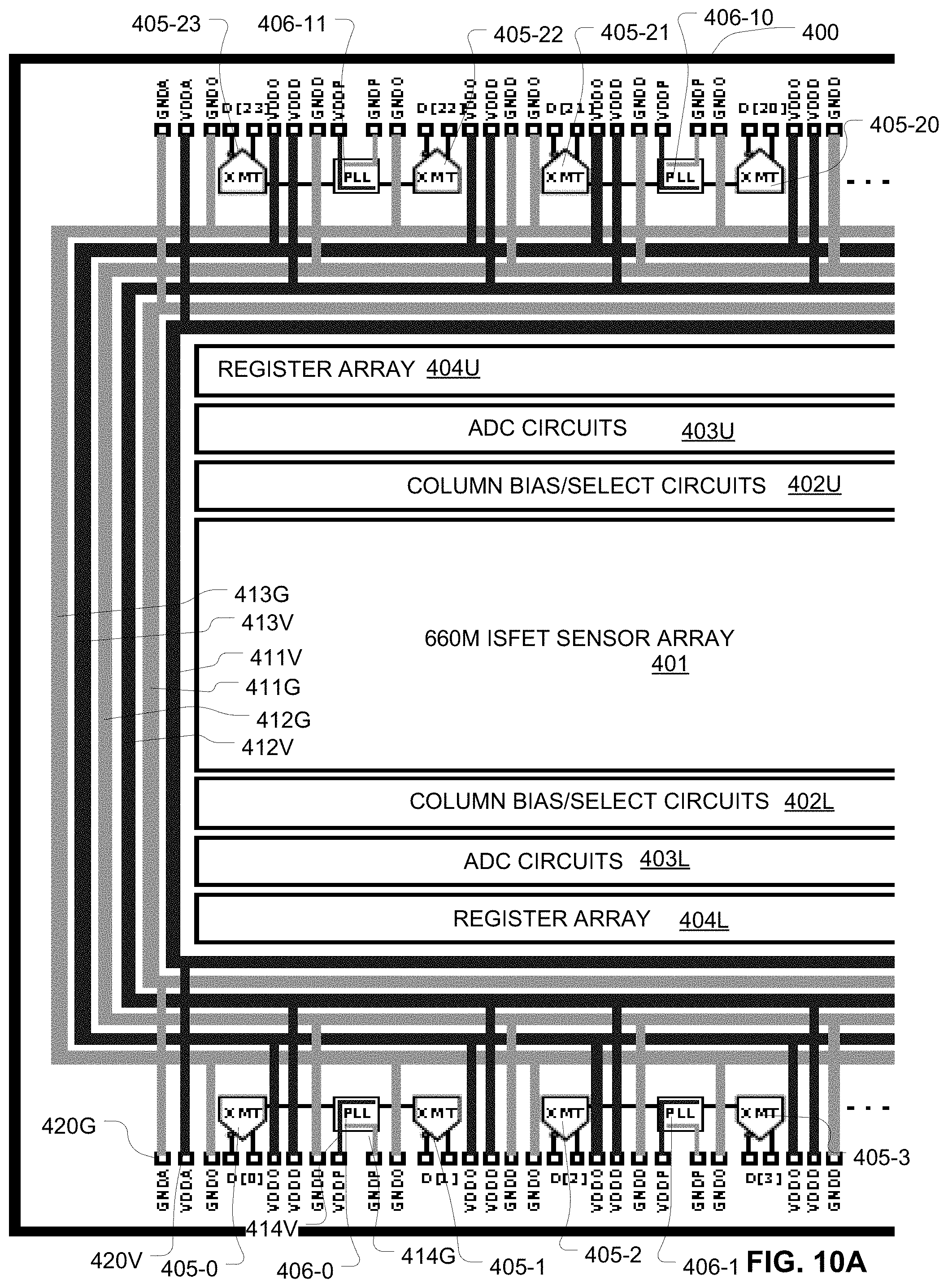
[0023] FIGS. 10A and 10B illustrate a layout of power supply traces and pads for a multiple power domain integrated circuit as described herein.
[0024] FIG. 11 is an expanded view of the power supply trace and pad layout for a portion of the integrated circuit shown in FIGS. 10A and 10B.
[0025] FIG. 12 illustrates a part of an electrostatic discharge protection network which may be used for the multiple power domain integrated circuit described herein.
[0026] FIG. 13 illustrates another part of an electrostatic discharge protection network which may be used for the multiple power domain integrated circuit described herein.
DETAILED DESCRIPTION
[0027] A detailed description of embodiments of the sensor technology and components thereof is provided with reference to FIGS. 1-13.
[0028] FIG. 1 illustrates a block diagram of components of a system for nucleic acid sequencing according to some embodiments. Such systems include device 100, which acts as a source of data that produces over 50 Gb per second of digital data, and in examples described herein, may produce over 100 Gb per second, and more. As illustrated schematically, a communication bus 127 supporting over 100 Gb per second may be desired in embodiments of the technology described herein. In an example system, a sensor chip includes over 600 million sensors, producing multiple bits per sensor, and senses at high frame rates. Additionally, a massively parallel system for transmitting data from a sensor array, or other high data rate source of data, on an integrated circuit, to a destination processor is described herein.
[0029] As shown in FIG. 1, a nucleic acid sequencing system may include flow cell 101 on integrated circuit device 100, reference electrode 108, a plurality of reagents 114 for sequencing, valve block 116, wash solution 110, valve 112, fluidics controller 118, lines 120/122/126, passages 104/109/111, waste container 106, array controller 124, a reference clock 128 and user interface 129. As shown, integrated circuit device 100 includes microwell array 107 overlying a sensor array that includes devices as described herein. Flow cell 101 includes inlet 102, outlet 103, and flow chamber 105 defining a flow path of reagents over microwell array 107. Reference electrode 108 may be of any suitable type or shape, including a concentric cylinder with a fluid passage or a wire inserted into a lumen of passage 111. Reagents 114 may be driven through the fluid pathways, valves, and flow cell 101 by pumps, gas pressure, or other suitable methods, and may be discarded into waste container 106 after exiting outlet 103 of flow cell 101. Fluidics controller 118 can control driving forces for reagents 114 and operation of valve 112 (for wash fluid) and valve block 116 (for reagents) with a suitable processor executing software-implemented logic, other controller circuitry or combinations of controller circuitry and software-implemented logic. In some embodiments, fluidics controller 118 can control delivery of individual reagents 114 to flow cell 101 and integrated circuit device 100 in a predetermined sequence, for predetermined durations, and/or at predetermined flow rates.
[0030] Microwell array 107 includes an array of reaction regions which are operationally associated with corresponding sensors in the sensor array. For example, each reaction region may be coupled to one sensor or more than one sensor suitable for detecting an analyte or reaction property of interest within that reaction region. Microwell array 107 may be integrated in integrated circuit device 100, so that microwell array 107 and the sensor array are part of a single device or chip. Flow cell 101 can have a variety of configurations for controlling the path and flow rate of reagents 114 over microwell array 107.
[0031] Array controller 124 provides bias voltages and timing and control signals to integrated circuit device 100 for reading the sensors of the sensor array. Array controller 124 also provides a reference bias voltage the reference electrode 108 to bias reagents 114 flowing over microwell array 107.
[0032] Array controller 124 may also include a reader to collect output signals from the sensors of the sensor array through output ports on integrated circuit device 100 via bus 127, which comprises a plurality of high-speed serial channels for example, carrying sample data at speeds on the order of 100 gigabits per second or greater. In one example, twenty four serial channels, each of which nominally operates at 5 Gb per second, are implemented in the bus 127. A reference clock 128 may be coupled with the device 100 to provide a stable reference clock for use in controlling high-speed serial channels. In embodiments described herein, the reference clock 128 can operate at relatively low frequencies, on the order of 100 MHz or 200 MHz. Alternatively, the reference clock may operate at data rates desired to support the high-speed serial channels. Array controller 124 can include a data processing system, with a reader board including a set of field programmable gate arrays (FPGAs), having a plurality of receivers in support of the transmitters on the device 100. Array controller 124 can include memory for storage of data and software applications, a processor for accessing data and executing applications, and components that facilitate communication with the various components of the system in FIG. 1.
[0033] The values of the output signals of the sensors can indicate physical and/or chemical parameters of one or more reactions taking place in the corresponding reaction regions in microwell array 107. For example, in some exemplary embodiments, the values of the output signals may be processed using the techniques disclosed in Rearick et al., U.S. patent application Ser. No. 13/339,846, filed Dec. 29, 2011, and in Hubbell, U.S. patent application Ser. No. 13/339,753, filed Dec. 29, 2011, which are all incorporated by reference herein in their entirety. User interface 129 can display information about flow cell 101 and the output signals received from sensors in the sensor array on integrated circuit device 100. User interface 129 can also display instrument settings and controls, and allow a user to enter or set instrument settings and controls.
[0034] Array controller 124 can collect and analyze the output signals of the sensors related to chemical and/or biological reactions occurring in response to the delivery of reagents 114. The system can also monitor and control the temperature of integrated circuit device 100 so that reactions take place and measurements are made at a known predetermined temperature. The system may be configured to let a single fluid or reagent contact reference electrode 108 throughout an entire multi-step reaction during operation. Valve 112 may be shut to prevent any wash solution 110 from flowing into passage 109 as reagents 114 are flowing. Although the flow of wash solution may be stopped, there can still be uninterrupted fluid and electrical communication between reference electrode 108, passage 109, and microwell array 107. The distance between reference electrode 108 and the junction between passages 109 and 111 may be selected so that little or no amount of the reagents flowing in passage 109, which may diffuse into passage 111, will reach reference electrode 108. In some embodiments, wash solution 110 may be selected as being in continuous contact with reference electrode 108, which may be especially useful for multi-step reactions using frequent wash steps.
[0035] FIG. 2 illustrates a cross-sectional view of a portion of an exemplary integrated circuit device 200, flow cell 201 and reference electrode 208. The device includes a sensor array (schematically 205) coupled to a microwell array (schematically 207). During operation, flow chamber 204 of flow cell 201 confines reagent flow 206 of delivered reagents across open ends of the reaction regions in microwell array 207. The volume, shape, aspect ratio (such as base width-to-well depth ratio), and other dimensional characteristics of the reaction regions may be selected based on the nature of the reaction taking place, as well as the reagents, products/byproducts, or labeling techniques (if any) that are employed. The sensors of sensor array 205 may be responsive to (and generate output signals related to) chemical and/or biological reactions within associated reaction regions in microwell array 207 to detect an analyte or reaction property of interest. The sensors of sensor array 205 may be chemically sensitive field-effect transistors (chemFETs), such as ion-sensitive field effect transistors (ISFETs). Examples of sensors and array configurations that may be used in embodiments are described in U.S. Patent Application Publication No. 2010/0300559, filed May 24, 2010, No. 2010/0197507, filed Oct. 5, 2012, No. 2010/0301398, filed Oct. 5, 2012, No. 2010/0300895, May 4, 2010, No. 2010/0137143, filed May 29, 2009, and No. 2009/0026082, filed Dec. 17, 2007, and U.S. Pat. No. 7,575,865, filed Aug. 1, 2005, each of which are incorporated by reference herein in their entirety.
[0036] The integrated circuit device 200 includes a large number of serial ports supporting connection to a massively parallel reader 211 via a set of serial channels 210. The reagent flow 206, coupled with a large array of ISFETs, presents a complex electrical and mechanical environment in which such a massively parallel communication system can operate with high integrity.
[0037] In some embodiments, other types of sensor arrays may be used in systems like that of FIG. 1, including but not limited to arrays of thermistors and arrays of optical sensors, for example.
[0038] FIG. 3 illustrates cross-sectional view of representative sensors/detectors and corresponding reaction regions according to an exemplary embodiment. In some embodiments the sensors may be chemical sensors. FIG. shows 3 two exemplary sensors 350, 351, representing a small portion of a sensor array that can include millions of sensors; even billions of sensors are contemplated. For example, the sensor array can comprise between 100 and 1,000 sensors, between 100 and 10,000 sensors, between 10,000 and 100,000 sensors, between 100,000 and 1,000,000 sensors, between 1,000,000 and 40,000,000 sensors, between 10,000,000 and 165,000,000 sensors, between 100,000,000 and 660,000,000 sensors, between 1,000,000,000 and 5,000,000,000 sensors, between 5,000,000,000 and 9,000,000,000 sensors, and up to 10,000,000,000 sensors. Windowing of the array is contemplated such that data can be obtained from all or fewer than all of the sensors. Sensor 350 is coupled to corresponding reaction region 301, and sensor 351 is coupled to corresponding reaction region 302. The two illustrated reaction regions are chemically and electrically isolated from one another and from neighboring reaction regions. The dielectric material 303 defines the reaction regions 301/302 which may be within an opening defined by an absence of dielectric material. Dielectric material 303 can comprise one or more layers of material, such as silicon dioxide or silicon nitride or any other suitable material or mixture of materials. The dimensions of the openings, and their pitch, can vary from embodiment to embodiment. In some embodiments, the openings can have a characteristic diameter, defined as the square root of 4 times the plan view cross-sectional area (A) divided by Pi (e.g., sqrt(4*A/.pi.), of not greater than 5 micrometers, such as not greater than 3.5 micrometers, not greater than 2.0 micrometers, not greater than 1.6 micrometers, not greater than 1.0 micrometers, not greater than 0.8 micrometers, not greater than 0.6 micrometers, not greater than 0.4 micrometers, not greater than 0.2 micrometers or not greater than 0.1 micrometers. The plan view area of the sensor is determined in part by the width (or diameter) of reaction regions and may be made small to provide a high density array. The footprint of a sensor may be determined and/or reduced by modifying the width (e.g. diameter) of the reaction region. In some embodiments, the density of the array may be increased or decreased based on the diameter selected for the reaction region. Low noise sensors may be provided in a high density array by reducing device and interconnect overhead, including gate area and contact area. Additional examples of sensors and their corresponding reaction regions according to additional exemplary embodiments are described in Fife et al., U.S. patent application Ser. No. 14/198,382, filed Mar. 5, 2014, based on U.S. Prov. Pat. Appl. Nos. 61/868,739, filed Aug. 22, 2013, and 61/790,866, filed Mar. 15, 2013; Fife et al., U.S. patent application Ser. No. 14/197,710, filed Mar. 5, 2014, based on U.S. Prov. Pat. Appl. Nos. 61/868,736, filed Aug. 22, 2013, and 61/790,866, filed Mar. 15, 2013; Fife et al., U.S. patent application Ser. No. 14/198,402, filed Mar. 5, 2014, based on U.S. Prov. Pat. Appl. Nos. 61/868,942, filed Aug. 22, 2013, and 61/790,866, filed Mar. 15, 2013; Fife et al., U.S. patent application Ser. No. 14/197,741, filed Mar. 5, 2014, based on U.S. Prov. Pat. Appl. Nos. 61/868,947, filed Aug. 22, 2013, and 61/790,866, filed Mar. 15, 2013; and Fife et al., U.S. patent application Ser. No. 14/198,417, filed Mar. 5, 2014, based on U.S. Prov. Pat. Appl. Nos. 61/900,907, filed Aug. 22, 2013, and 61/790,866, filed Mar. 15, 2013, which are all incorporated by reference herein in their entirety.
[0039] Sensor 350 is representative of the sensors in the sensor array. In the illustrated example, sensor 350 is a chemically-sensitive field effect transistor (chemFET), more specifically an ion-sensitive field effect transistor (ISFET) in this example. Sensor 350 includes floating gate structure 318 having sensor plate 320 coupled to reaction region 301 by electrode 307 which can have a surface adapted for contact with an electrolyte (an ionic conducting liquid). Sensor plate 320 is the uppermost floating gate conductor in floating gate structure 318. In the illustrated example, floating gate structure 318 includes multiple patterned layers of conductive material within layers of dielectric material 319. Sensor 350 also includes conduction terminals including source/drain region 321 and source/drain region 322 within semiconductor substrate 354. Source/drain region 321 and source/drain region 322 comprise doped semiconductor material having a conductivity type different from the conductivity type of substrate 354. For example, source/drain region 321 and source/drain region 322 can comprise doped P-type semiconductor material, and the substrate can comprise doped N-type semiconductor material. Channel region 323 separates source/drain region 321 and source/drain region 322. Floating gate structure 318 overlies channel region 323, and is separated from substrate 354 by gate dielectric 352. Gate dielectric may be silicon dioxide, for example. Alternatively, other suitable dielectrics may be used for gate dielectric 352 such as, for example materials with higher dielectric constants, silicon carbide (SiC), silicon nitride (Si.sub.3N.sub.4), Oxynitride, aluminum nitride (AlN), hafnium dioxide (HfO.sub.2), tin oxide (SnO.sub.2), cesium oxide (CeO2), titanium oxide (TiO2), tungsten oxide (WO3), aluminum oxide (Al2O3), lanthanum oxide (La2O3), gadolinium oxide and others, and any combination thereof.
[0040] In some embodiments, sensor 350 includes electrode 307 overlying and in communication with an uppermost floating gate conductor in the plurality of floating gate conductors. Upper surface 308 of electrode 307 defines a bottom surface of a reaction region for the sensor. Upper surface 308 of electrode 307 can act as the sensor surface of the sensitive area for sensor 350. Electrode 307 can comprise one or more of a variety of different materials to facilitate sensitivity to particular ions. For example, silicon nitride or silicon oxynitride, as well as metal oxides such as silicon oxide, aluminum or tantalum oxides, generally provide sensitivity to hydrogen ions, whereas sensing materials comprising polyvinyl chloride containing valinomycin provide sensitivity to potassium ions. Materials sensitive to other ions such as sodium, silver, iron, bromine, iodine, calcium, hydroxide, phosphate, and nitrate can also be used. In the illustrated example, electrode 307 is shown as a single layer of material. More generally, the electrically electrode can comprise one or more layers of a variety of electrically conductive materials, such as metals or ceramics, or any other suitable conductive material or mixture of materials, depending upon the implementation. The conductive material may be any suitable metallic material or alloy thereof, or may be any suitable ceramic material, or a combination thereof. Examples of metallic materials include aluminum, copper, nickel, titanium, silver, gold, platinum, hafnium, lanthanum, tantalum, tungsten, iridium, zirconium, palladium, or any suitable material or combination thereof. Examples of ceramic materials include one of titanium nitride, titanium aluminum nitride, titanium oxynitride, tantalum nitride, or any suitable combination thereof. In some embodiments, an additional sensing material (not shown) is deposited on upper surface 308 of electrode 307. In some embodiments, the electrode may be titanium nitride, and titanium oxide or titanium oxynitride may be grown on the upper surface 308 during manufacturing and/or during exposure to fluids during use. Whether an oxide is formed on the upper surface depends on the conductive material used, the manufacturing processes performed, and/or the conditions under which the sensor is operated. The electrode may be formed in various shapes (width, height, etc.) depending on the materials and/or etch techniques and/or fabrication processes etc. used during the manufacture process.
[0041] In some embodiments, reactants, wash solutions, and other reagents can move in and out of reaction region 301 by diffusion mechanism. Sensor 350 is responsive to (and can generate an output signal related to) charge 324 proximate to electrode 307. For example, when the sensor is coupled to an electrolyte, the sensor may be responsive to an electrolytic potential at the sensor surface. The responsiveness of the sensor can relate to the amount of charge that is present proximate to the electrode 307. The presence of charge 324 in an analyte solution can alter the surface potential at the interface between the analyte solution and upper surface 308 of electrode 307. For example, the surface potential may be altered by protonation or deprotonation of surface groups caused by the ions present in the analyte solution. In another example, the charge of surface functionality or absorbed chemical species may be altered by analytes in solution. Changes in the amount of charge present can cause changes in the voltage on floating gate structure 318, which in turn can cause an effective change in the threshold voltage of the transistor of sensor 350. The potential at the interface may be measured by measuring the current in channel region 323 between source region 321 and drain region 322. As a result, sensor 350 may be used directly to provide a current-based output signal on an array line connected to source region 321 or drain region 322, or indirectly with additional circuitry to provide a voltage-based output signal. Charge may be more highly concentrated near the bottom of reaction region 301. Accordingly, in some embodiments variations in the dimensions of the electrode can have an effect on the amplitude of the signal detected in response to charge 324.
[0042] In some embodiments, reactions carried out in reaction region 301 may be analytical reactions to identify or determine characteristics or properties of an analyte of interest. Such reactions can generate directly or indirectly products/byproducts that affect the amount of charge adjacent to electrode 307. If such products/byproducts are produced in small amounts or rapidly decay or react with other constituents, multiple copies of the same analyte may be analyzed in reaction region 301 at the same time in order to increase the output signal generated. In some embodiments, multiple copies of an analyte may be attached to solid phase support 312, either before or after being deposited into reaction region 301. Solid phase support 312 may be a particle, a microparticle, a nanoparticle. In some embodiments, the analyte may be attached to a bead which may be solid or porous and can further comprise a gel, or the like, or any other suitable solid support that may be introduced to a reaction region. In some embodiments, copies of an analyte may be located in a solution proximal to a sensor of a reaction region. Alternatively, copies of an analyte can bind directly to the surface of the sensor to capture agents includes the material on the surface or if there are pores on the surface (for example, copies of an analyte can bind directly to electrode 307). The solid phase support may be of varied size, for example, in a range of 100 nm to 10 micrometers. Further, the solid support may be positioned in the opening at various places. For a nucleic acid analyte, multiple, connected copies may be made by rolling circle amplification (RCA), exponential RCA, polymerase chain reaction (PCR) or like techniques, to produce an amplicon without the need of a solid support.
[0043] In various exemplary embodiments, the methods, and systems described herein can advantageously be used to process and/or analyze data and signals obtained from a biological reaction, including amplification or electronic or charged-based nucleic acid sequencing. In electronic or charged-based sequencing (such as pH-based sequencing), a nucleotide incorporation event may be determined by detecting ions (e.g., hydrogen ions) that are generated as natural products of polymerase-catalyzed nucleotide extension reactions. The detection of a nucleotide incorporation event may be used to sequence a sample or template nucleic acid, which may be a fragment of a nucleic acid sequence of interest, for example, and which may be directly or indirectly attached as a clonal population to a solid support. In some embodiments, the solid support can be a particle or a microparticle. In some embodiments, the nucleic acid sequence can be attached to a bead. The sample or template nucleic acid may be operably associated to a primer and polymerase and may be subjected to repeated cycles or "flows" of deoxynucleoside triphosphate ("dNTP") addition (which may be referred to herein as "nucleotide flows") from which nucleotide incorporations can result and washing. The primer may be annealed to the sample or template so that the primer's 3' end may be extended by a polymerase whenever dNTPs complementary to the next base in the template are added. Based on the known sequence of nucleotide flows and on measured output signals of the sensors indicative of ion concentration during each nucleotide flow, the identity of the type, sequence and number of nucleotide(s) associated with a sample nucleic acid present in a reaction region coupled to a sensor may be determined.
[0044] FIG. 4 is a simplified block diagram of part of the circuitry on an integrated circuit sensor array used for DNA sequencing. The integrated circuit includes a 660 megapixel ISFET sensor array 401 on a substrate 400. An upper set of column bias/select circuits 402U and an upper row decoder (row dec) 531 are configured for access to an upper half of the array 401. A lower set of column bias/select circuits 402L and a lower row decoder 521 are configured for access to a lower half of the array 401.
[0045] An upper set of analog-to-digital converter (ADC) circuits 403U is coupled to the upper set of column bias/select circuits 402U. An upper register array 404U is coupled to the upper set of analog-to-digital converter circuits 403U. The upper register array 404U may be configured to provide a plurality of streams of digital data through serializers (e.g. 511, 512) to corresponding transmitters (e.g. 405-23, 405-22). Each of the transmitters is coupled to a corresponding pair (a pair for D[23], a pair for D[22]) of output pads, which in turn are connected to transmission lines (not shown).
[0046] Likewise, a lower set of analog-to-digital converter circuits 403L is coupled to the lower set of column bias and select circuits 402L. A lower register array 404L is coupled to the lower set of analog-to-digital converter circuits 403L. The lower register array 404L may be configured to provide a plurality of streams of digital data through serializers (e.g. 501, 502) to corresponding transmitters (e.g. 405-0, 405-1). Each of the transmitters is coupled to a corresponding pair (D[0], D[1]) of output pads, which in turn are connected to transmission lines (not shown).
[0047] The configurations described herein support a device having a large number of gigabit per second transmitters, such as at least 20 transmitters capable of transmission at a data rate greater than 1 Gb per second, and configured in at least 10 pairs. Large numbers of gigabit per second transmitters present a context in which a class of implementation problems arises which not apparent in configurations with small numbers of transmitters. For one example, the device includes 24 transmitters capable of transmitting data at 5 Gb per second each, or faster, supporting throughput from a high speed data source of 120 Gb per second or more.
[0048] Supporting peripheral circuitry including a sequencer 532, a digital-to-analog converter 533, a gray code generator 534, and bias circuitry 535 are coupled to the upper circuitry. Also, supporting circuitry including a sequencer 522, a digital-to-analog converter 523, a gray code generator 524, and bias circuitry 525 are coupled to the lower circuitry. The chip includes a serial peripheral interface (SPI) control block 540 to support the serial ports on the device, and a fuse array 541 used in configuration of the device.
[0049] In one example operating technique, sequencer logic 522, 532 causes the circuitry to perform a frame sensing sequence. In a frame sequencing sequence, a row of ISFETs in each of the upper and lower halves of the array may be selected and biased using the upper/lower column bias/select circuits 402U/402L so that a current that may be a function of the charge in that corresponding sensor well may be produced on each column line. The upper/lower analog-to-digital converter circuits 403U/403L receive a ramp signal from the digital-to-analog converter 533, 523, and produce an output signal when the current on the corresponding column line matches the level of the ramp signal. The gray code generator 524, 534 may be sampled in response to the output signal, and the results are stored in the upper/lower register array 404U/404L. Data in the register array 404U/404L are assembled into packets, and applied in a plurality of digital data streams to the transmitters on the chip.
[0050] The illustrated part of the circuitry in FIG. 4 includes four transmitters out of a set of 24 transmitters on the substrate 400. The four transmitters illustrated include a first pair of transmitters 405-0, 405-1, and a second pair of transmitters 405-22, 405-23. As shown, one phase locked loop 406-0, including a low pass filter, is coupled to the first pair of transmitters 405-0, 405-1. Also, one phase locked loop 406-11, including a low pass filter, is coupled to the second pair of transmitters 405-22, 405-23. The phased locked loops operate as clock multipliers, each of which produces a local transmit clock and provides the local transmit clock to the transmitter on its left and to the transmitter on its right via clock lines (e.g. 407a, 407b at phase locked loop 406-0).
[0051] Each phase locked loop/low pass filter, 406-0, 406-11, is coupled with corresponding phase locked loop control block 503, 513 which stores parameters used to control and calibrate phase locked loop. This pattern may be repeated across the 24 transmitters on the chip, so that there are 12 phase locked loop blocks, and 24 transmitters. The transmitters are grouped into pairs which are coupled to individual phase locked loops. The phase locked loops are disposed on the substrate between the transmitters, so that the transmission distance from the phase locked loop to the transmitter using the clock produced in the phase locked loop may be small.
[0052] As illustrated, each of the phase locked loops 406-0, 406-11 is coupled to an individual power pad VDDP and an individual ground pad GNDP. Also, the individual power pad VDDP and the individual ground pad GNDP for each phase locked loop are disposed on the chip adjacent the phase locked loop, and between the output pads for the transmitter on the left, and the output pads for the transmitter on the right in the corresponding transmitter pair.
[0053] The individual power pad VDDP and the individual ground pad GNDP are connected to an off-chip voltage supply, which may be configured with bypass capacitors and other circuitry, to create a low noise power configuration for the phase locked loop circuits, and to reduce coupling of noise between the high-frequency phase locked loop circuits and other circuits on the substrate 400. A low-speed reference clock (not shown, see FIG. 5) may be distributed on the chip and connected to each of the phase locked loops. The clock multipliers in the illustrated embodiment are implemented using phase locked loops. Clock multipliers may be implemented using other circuitry as well, such as delay locked loops, phase interpolators, and combinations of phase locked loops, phase interpolators and/or delay locked loops.
[0054] FIG. 5 illustrates clock distribution circuitry which may be utilized with a device like that shown in FIG. 4. The clock distribution circuitry includes a clock input buffer 570 which includes CLKP and CLKN inputs configurable to receive a differential clock signal or a single ended clock signal from an off-chip clock reference. The output of the clock buffer 570 may be distributed in a daisy chain fashion to the phase locked loops 580-0 through 580-5 disposed along a lower side of the chip, and through a duty cycle correction DCC chain 571, which includes a group of cascaded DCC buffers to support transmission of the reference clock across the large chip, to the phase locked loops 580-6 through 580-11 along an upper side of the chip. In this example, the reference clock may be distributed to the transmitter units xmt0 to xmt11 on the lower side and via the DCC chain 571 to transmitter units xmt12 to xmt23 on the upper side. Each of the transmitter units includes a duty cycle correction DCC buffer, and passes the reference clock from the DCC buffer in the transmitter unit to its adjacent phase locked loop, or adjacent transmitter unit. An example of the transmitter unit circuitry including this DCC buffer is described below with reference to FIG. 7. In alternatives, the reference clock may be coupled directly to the phase locked loop circuit, and DCC buffers may be disposed on the chip in other configurations as necessary. The clock distribution circuit provides a reference clock at a relatively low frequency, such as 125 MHz, with a 50% duty cycle to each of the phase locked loops. In this example, the reference clock may be distributed asynchronously to the phase locked loops.
[0055] FIG. 6 is a block diagram of the clock input buffer 570 shown in FIG. 5. The clock input buffer 570 in this example includes a multiplexer 991. The CLKP pad is connected to both the "0" and "1" inputs of the multiplexer 991. The CLKN pad is connected to the "0" input of the multiplexer 991. A parameter set on the device, labeled cmos_sel in the figure, controls the multiplexer 991 so that it converts the differential input in one mode to a single ended output, or provides the single ended input through as the single ended output. The single ended output of the multiplexer 991 may be supplied through a NAND gate 992 to a DCC buffer (dcc) 993. The NAND gate 992 may be controlled by a control signal labeled ref_sel in this example. The output of the DCC buffer 993 may be the reference clock to be distributed on the chip.
[0056] A duty cycle correction circuit, such as that used for element 993, or used in the DCC chain 571 described with reference to FIG. 5, may be implemented using a variety of circuit structures. Examples are described in the literature, including Ogawa, et al., "A 50% DUTY-CYCLE CORRECTION CIRCUIT FOR PLL OUTPUT," IEEE International Symposium on Circuits and Systems (Volume: 4) ISCAS 2002; M. Ragavan, et al. "DUTY CYCLE CORRECTOR WITH SAR FOR DDR DRAM APPLICATION," International Journal of Advanced Research in Electrical, Electronics and Instrumentation Engineering, Vol. 2, Issue 5, May 2013.
[0057] FIG. 7 illustrates a configuration of a transmitter pair according to embodiments of the technology described herein. Each transmitter pair includes first transmitter XMT 610 and second transmitter XMT 611, which in this example correspond to the transmitter for output D[0] and the transmitter for output D[1] on the chip. A phase locked loop/low pass filter circuit 612 may be disposed between the transmitters 610, 611 in the pair. Transmitter control blocks 620, 621 are coupled to the corresponding transmitters 610, 611. Corresponding data streams 630, 631 are input to the transmit control block 620, 621 from the register array on the chip, respectively. A phase locked loop control block 622 is coupled to the phase locked loop/low pass filter 612.
[0058] Three power domains are implemented in the transmitter pair configuration shown in FIG. 7. Transmitter control blocks 620, 621, and PLL control block 622 receive power in a digital power domain based on the supply terminals VDDD and GNDD. The transmitters 610, 611 receive power in a transmitter power domain (output "O" power) based on supply terminals VDDO, GNDO. The phase locked loop/low pass filter circuits are disposed in individual power domains based on supply terminals VDDP, GNDP that are directly connected to the phase locked loop/low pass filter circuitry.
[0059] The reference clock RCLK is coupled to the phase locked loop from clock distribution circuitry, like that described above. A system clock SCLK is coupled to the transmitter control blocks 620, 621, and PLL control block 622. The system clock can operate nominally at the same frequency as the reference clock in some embodiments, but may be a different frequency. The phase locked loop 612 operates as a clock multiplier, producing a high speed, local transmit clock on line 650.
[0060] In one example, the system clock and reference clock operate at 125 MHz. The high-speed, local transmit clock may be produced at 2.5 GHz (20.times. multiplication). The transmitters in this example transmit on both the rising and falling edges of the local transmit clock, resulting in a transmission rate of 5 Gb per second. In a chip having 24 transmitters operating at 5 Gb per second, a throughput of 120 Gb per second may be achieved.
[0061] High data integrity of the transmitted data is supported using techniques including distribution of a low-speed reference clock, the configuration of the phase locked loops in individual power domains, the placement of the phase locked loops between corresponding pairs of transmitters, and local use of the locally produced high-speed transmit clocks.
[0062] FIG. 8 is a block diagram of a transmitter and transmitter control block 700 which may be used in the configuration shown in FIGS. 5 and 7. A reference clock (refclk) may be supplied as input to a single output, duty cycle correction buffer (dcc1) 710. The output of the DCC buffer 710 may be applied as an output (refclk0) for connection in daisy chain fashion as illustrated in FIG. 5. Also, the output of DCC buffer 710 may be supplied to a clock selector 711, which also includes a differential output DCC buffer. Clock selector 711 is capable of selecting between the local high-speed transmit clock, labeled PLLclk in this example, and the reference clock output from the DCC buffer 710. A control signal (rclk_sel) may be used to determine the selection. The ability to select the reference clock output from DCC buffer 710 supports testing the chip. In operating mode, the local high-speed transmit clock PLLclk may be selected. The output of the clock selector 711 may be a duty cycle-corrected, differential clock on lines 720, at the local transmit clock frequency.
[0063] The differential clock on lines 720 may be supplied to a synchronizer circuit (sync) 701, a serializer circuit (serializer) 702, a pre-driver 703, and an off-chip driver 704. The output of the off-chip driver is connected to the pads OUTP and OUTN, which are in turn connected to a transmission line. The synchronizer circuit 701 also receives the system clock (sys clk), and produces a synchronized system clock for the serializer 702. The data stream from the register arrays are applied in this example in 20 bit packets to the serializer 702. The output of the serializer may be applied to the pre-driver 703, and then off chip via the off-chip driver 704.
[0064] FIG. 9 is a block diagram of a phase locked loop 800 including a low pass filter, which may be utilized in the configuration of FIGS. 5 and 7. The phase locked loop 800 includes a phase and frequency detector (PFD) 801 connected to the reference clock (ref clk), a charge pump 802, a low pass filter 803, and a ring voltage controlled oscillator (VCO) 804. A programmable divider 805 is connected between the output of the ring VCO 804, and the input of the phase and frequency detector 801. The programmable divider 805 in this example includes a clock selector 811, a first divider 810, and a second divider 812. The clock selector 811 receives the output of the ring VCO 804 at one input, and the output of the divider 810 on a second input. The divider 810 in this example may be a divide-by-two block (/2). A control signal div<0> controls the clock selector 811. The output of the clock selector 811 may be applied as the local high-speed transmit clock pllclk. The output of the divider 810 may be applied to the input of the second divider 812. The second divider is configurable to divide by five (0:/5), or to divide by 10 (0:/10), in response to a control signal div<1>. In combination, during operation, combination of the first divider 810 and the second divider 812 provides a divide-by-20 operation in the 5 Gb per second example described above so that, in effect, the local high-speed transmit clock can operate at 20 times the frequency of the reference clock.
[0065] A variety of control parameters are coupled to the various blocks in the phase locked loop 800. Parameters "fast, lock, slow" are provided from the phase and frequency detector 801 to control circuitry. Charge pump bias parameters bias_CP<3:0> are applied to the charge pump 802. Low pass filter parameters C1<5:0> and C2<4:0> are applied to the low pass filter 803. VCO control parameters band ctl<3:0> are applied to the ring VCO 804. The phase locked loop may be digitally controlled using basic phase locked loop management for calibration and configuration, driven by link control logic on the reader board in one example. In other embodiments, phase locked loop calibration and configuration may be locally driven, or a combination of local and remote operations may be utilized.
[0066] The low pass filter in the phase locked loop may be configured with a transfer function that rejects jitter in the reference clock. This may be implemented in the charge pump and filter circuitry in the loop as it operates on the output of the phase and frequency detector nominally at the frequency of the reference clock.
[0067] FIGS. 10A and 10B illustrate layout of the transmitter circuits and power traces of an example sensor integrated circuit, in support of a multiple power domain system. The reference numerals used in FIG. 4 are used again for like components. Thus, the device includes a substrate 400. A 660 megapixel ISFET sensor array 401 may be implemented on the substrate. Upper and lower column bias and select circuits 402U, 402L, respectively, upper and lower analog-to-digital converter circuits 403U, 403L, respectively, and upper and lower register arrays 404U, 404L respectively, are implemented in the central region of the chip. Twelve transmitter pairs are disposed around the perimeter of the chip, with six pairs on the lower side of the chip, and six pairs on the upper side of the chip. The plurality of transmitter pairs includes first transmitter pair 405-0, 405-1, and second transmitter pair 405-2, 405-3, illustrated in FIG. 10A; and transmitter pair 405-8, 405-9, transmitter pair 405-10, 405-11 illustrated in FIG. 10B on the lower edge. Also, the plurality of transmitter pairs includes transmitter pair 405-12, 405-13 and transmitter pair 405-14, 405-15 illustrated in FIG. 10B and transmitter pair 405-20 405-21 transmitter pair 405-22 405-23 illustrated in FIG. 10A on the upper edge. Four additional transmitter pairs are implemented on the chip along the upper and lower edges, but are omitted from the drawing because of the cutout. Thus, 12 transmitter pairs are implemented on the substrate 400, for a total of 24 transmitters. As described above, each transmitter pair includes a local clock multiplier, implemented in this example by a phase locked loop with a low pass filter. Thus, FIGS. 10A and 10B show phase locked loops 406-0, 406-1, 406-4, 406-5, 406-6, 406-7, 406-10, and 406-11 each of which may be placed on the substrate between the transmitters in a corresponding pair of transmitters.
[0068] FIGS. 10A and 10B illustrate an example of a substrate that includes one or more power domains for a high data rate data source, such as the array of ISFETs illustrated, for the transmitters and for peripheral logic including reference clock distribution circuitry. In the layout of FIGS. 10A and 10B, the clock multipliers are disposed on the substrate in individual power domains separate from one another and from the other one or more power domains.
[0069] FIGS. 10A and 10B illustrate a configuration of power pads and power traces on the chip to support multiple power domains. The power domains include an analog power domain GNDA, VDDA, a digital power domain GNDD, VDDD, and a transmitter power domain GNDO, VDDO. In addition, the power domains include 12 individual power domains, one for each phase locked loop. The power pads are conductive pads on the substrate 400 adapted for connection to a pin or other connector structure for an electrical connection to off-chip structures. Such power pads often include a pad of patterned metal in the highest metal layer on the device. The power traces are conductive traces on the substrate adapted for distributing power across a region of the substrate. Such power traces are often implemented in the highest patterned metal layer on the device, and have relatively large width dimensions to support carrying a significant amount of current.
[0070] The analog power domain includes power pads labeled GNDA, VDDA on each of the four corners of the substrate 400. The analog power domain includes a power bus including a trace 411V connected to the VDDA power pads (e.g. 420V in the lower left), and a trace 411G connected to the GNDA power pads (e.g. 420G in the lower left). Traces 411V and 411G are configured on the device as the inside power traces, and surround the analog core of the device, which includes the sensor array 401, and portions of the other circuitry.
[0071] The digital power domain includes power pads labeled GNDD, VDDD distributed in pairs around the perimeter of the chip, including one pair between each transmitter. The digital power domain includes a power bus including a trace 412V connected to the VDDD power pads, and a trace 412G connected to the GNDD power pads. The traces 412V and 412G are placed on the device just outside the analog power domain traces 411V and 411G, and are placed adjacent digital circuitry surrounding the analog core of the chip.
[0072] The transmitter power domain includes power pads labeled GNDO, VDDO distributed in pairs around the perimeter of the chip, with one pair for every transmitter. Each pair of transmitter power domain power pads includes a GNDO pad on one side of the corresponding transmitter, and a VDDO pad on the opposite side of the corresponding transmitter. The transmitter power domain includes a power bus including trace 413V connected to the VDDO power pads and a trace 413G connected to the GNDO power pads. The traces 413V and 413G are configured on the device just outside the digital power domain traces 412V and 412G, and are placed for distribution of power supply voltages to the transmitters on the perimeter of the chip.
[0073] In this example, each phase locked loop may be disposed in an individual power domain. Thus, for the chip including 12 phase locked loops (or other clock multipliers) coupled with 24 transmitters, there are 12 clock multiplier power domains. Each local clock multiplier power domain includes a pair of power pads labeled GNDP, VDDP in the figure. The power pads GNDP and VDDP are disposed between the output pads for the transmitters. Thus, the power pads GNDP and VPPD for the phase locked loop 406-0 are disposed between the output pads for serial channel D[0] and the output pads for serial channel D[1]. Each local clock multiplier power domain includes a power trace and a ground trace confined to the phase locked loop circuitry. Thus, phase locked loop 406-0 includes a power trace 414V and a ground trace 414G. Likewise, phase locked loop 406-7 in FIG. 10B includes a power trace 415V and a ground trace 415G connected to the local power pad VDDP and ground pad GNDP respectively.
[0074] As may be seen from FIGS. 10A and 10B, the substrate 400 includes 12 pairs of transmitters having individual clock multipliers disposed in individual power domains between the transmitters in the pair.
[0075] The circuits in each power domain, in addition to having separate power traces, and separate power and ground pads, are isolated electrically from one another. This isolation may be implemented using deep n-well technology for example, in which the active regions of the circuitry are implemented within one or more doped wells separated from the bulk substrate by a deep n-well. The deep n-well may be biased using a selected power supply voltage so that it remains reversed biased relative to the substrate and relative to the active region during operation. In this manner, noise produced in the ground and power circuitry is not coupled directly into the circuitry of other power domains via the substrate.
[0076] Some or all of the power domains may be isolated using other technologies, such as by formation of the active regions in semiconductor layers deposited over layers of insulating material, so the insulating material electrically separates the active regions from the substrate.
[0077] FIG. 11 illustrates two transmitter pairs taken from the layout of FIGS. 10A and 10B. FIG. 11 illustrates a transmitter pair 405-2, 405-3, with an individual phase locked loop 406-1 in between. Also, transmitter pair 405-8, 405-9 is shown, with an individual phase locked loop 406-4 in between. The phase locked loops have individual power pads and power traces. Thus, phase locked loop 406-1 includes the VDDP power pad connected to the power trace 417V, and the GNDP ground pad connected to the ground trace 417G. Phase locked loop 406-4 includes the VDDP power pad connected to the power trace 418V, and the GNDP ground pad connected to the ground trace 418G.
[0078] The pattern of power pads and output pads includes a set of 14 pads for each transmitter pair disposed around the substrate in a repeating sequence. The order from right to left for the set of 14 pads for the transmitter pair including transmitters 405-2 and 405-3, and phase locked loop 406-1 of the pads in this example is as follows: transmitter power domain ground pad GNDO, output pad pair D[2], transmitter power domain power pad VDDO, digital power domain power pad VDDD, digital power domain ground pad GNDD, local clock multiplier power pad VDDP, local clock multiplier ground pad GNDP, transmitter power domain ground pad GNDO, output pad pair D[3], transmitter power domain power pad VDDO, digital power domain power pad VDDD and digital power domain ground pad GNDD.
[0079] As mentioned above, in some embodiments one clock multiplier may be associated with only one transmitter, or with groups of more than two transmitters, as suits a particular need. One clock multiplier may be configured to provide a transmit clock to one or more transmitters, where the one or more transmitters are in a separate power domain than the power domain of the clock multiplier. A configuration in transmitter pairs can provide an advantage in that the length of a transmission line carrying the transmit clock from the clock multiplier to the adjacent transmitters in the transmitter pair may be configured locally and have short and uniform transmission paths, without traversing circuitry other than the clock multiplier and the connect transmitter.
[0080] FIG. 12 and FIG. 13 illustrate an electrostatic discharge ESD protection configuration for the plurality of power domains on a device such as that shown in FIGS. 10A and 10B. In each of FIGS. 12 and 13, the power and ground traces 411V, 411G, respectively, for the analog power domain, the power and ground traces 412V, 412G, respectively, for the digital power domain, and the power and ground traces 413V, 413G for the transmitter power domain are shown using the reference numbers of FIGS. 10A and 10B.
[0081] Referring to FIG. 12, an ESD protection array for protecting the ground and power pads and ground and power traces of each of the major power traces on the device is shown. The ESD circuits used include circuit 900 between the power and ground power pads (VDDA, GNDA) respectively, and power and ground traces (411V, 411G) for the analog power domain, circuits 901, 902 between the power and ground power pads (VDDD, GNDD) and power and ground traces (412V, 412G) for the digital power domain, and circuits 903, 904, 905 for the power and ground power pads (VDDO, GNDO) and power and ground traces (413V, 413G) in the transmitter power domain. The ESD circuits 900-905 may be implemented for example, utilizing reversed-biased diode configurations in a grounded gate NMOS (ggNMOS) technology connected between the power and the ground traces in the corresponding power domain. Other ESD circuit implementations may be used as well.
[0082] Referring to FIG. 13, an ESD protection array is illustrated for protecting the local clock multiplier power domains, and for cascading protection among the power traces of different power domains. In FIG. 13, the power trace 414V for an individual phase locked loop, and the ground trace 414G for the individual phase locked loop are shown. An ESD protection circuit 925 is connected between power and ground traces 414G and 414V respectively, and the corresponding pads VDDP, GNDP. Circuit 925 may be implemented using a reversed biased diode configuration in a grounded gate NMOS technology as well.
[0083] ESD protection circuits 910, 911, 912, and 913 are connected on one terminal to the power trace 411V connected to VDDA for the analog power domain. Circuit 910 is connected on its opposing terminal to the power trace 412V connected to VDDD in the digital power domain. Circuit 911 is connected on its opposing terminal to the power trace 413V connected to VDDO in the transmitter power domain.
[0084] A similar pattern may be distributed around the chip, so that circuit 912 is connected on its opposing terminal to the power trace 413V connected to VDDO in the transmitter power domain. Circuit 913 is connected on its opposing terminal to the power trace 412V connected to VDDD in the digital power domain.
[0085] A second tier of ESD circuits includes circuits 914, 915, 916 and 917, connected on one terminal to the analog ground trace 411G which is connected to the analog ground pad GNDA for the analog power domain. Circuit 914 is connected on its opposing terminal to the ground trace 412G connected to GNDD in the digital power domain. Circuit 915 may be connected on its opposing terminal to the ground trace 413G connected to GNDO in the transmitter power domain. A similar pattern may be distributed around the chip, so that circuit 916 is connected on its opposing terminal to the ground trace 413G connected to GNDO in the transmitter power domain. Circuit 917 is connected on its opposing terminal to the ground trace 412G connected to GNDD in the digital power domain.
[0086] The third tier the ESD circuits include circuits 918 and 919. Circuits 918, 919 each include one terminal coupled to the power trace 412V that is connected to VDDD in the digital power domain. Both of the circuits 918, 919 have opposing terminals connected to the power trace 413V that is connected to VDDO in the transmitter power domain.
[0087] A fourth tier of ESD circuits include circuits 920 and 921. Circuits 920 and 921 are both connected between the ground trace 412G that is connected to GNDD in the digital power domain, and the ground trace 413G that is connected to GNDO in the transmitter power domain.
[0088] Individual clock multiplier power domains are also protected by ESD circuits 926, 927 and 930. ESD circuits 926 and 927 have one terminal connected to the power trace 414V that is connected to the VDDP for the local clock multiplier power domain. Circuit 926 has an opposing terminal connected to the trace 411V that is connected to VDDA in the analog power domain. Circuit 927 has an opposing terminal connected to ground trace 413G in the transmitter power domain.
[0089] The ESD circuit 930 has one terminal connected to the ground trace 414G that is connected to GNDP of the local clock multiplier power domain, and an opposing terminal connected to the ground trace 413G that is connected to GNDO in the transmitter power domain.
[0090] Circuit 927 which is connected between a ground trace and a power trace, may be implemented using a reversed biased diode configuration in a grounded gate NMOS technology, consistent with the example given above for protection between power and ground traces.
[0091] The circuits which protect between power traces in different power domains, including the circuits 910, 911, 912, 913, 918, 919 and 926, may be implemented using a reversed biased diode configuration in a grounded gate NMOS technology, consistent with the example given above for protection between power and ground traces.
[0092] Circuits which protect between ground traces in different power domains, including the circuits 914, 915, 916, 917, 920, 921 and 930 may be implemented using back-to-back parallel diodes.
[0093] A manufacturing method for an integrated circuit includes forming a plurality of power domains on an integrated circuit; placing a data source comprising an analog sensor array on the substrate in an analog power domain; placing peripheral circuitry coupled to the sensor array to produce a plurality of streams of digital data using a system clock in a digital power domain; placing reference clock distribution circuitry on the substrate which distributes a reference clock having a reference frequency; placing in individual power domains a plurality of clock multipliers which produce respective local transmit clocks having transmit clock frequencies that are multiples of the reference clock frequency; routing the reference clock from the reference clock distribution circuitry to the plurality of clock multipliers; and placing a plurality of sets of transmitters on the substrate configured to receive corresponding streams of data from the data source; routing the local transmit clock from one clock multiplier in the plurality of clock multipliers to each set of transmitters.
[0094] A configuration for implementing an array of high-speed transmitters on an integrated circuit is described. Features of the implementation include local high-speed transmit clock generation, and provide a clock multiplier such as a phase locked loop, between each pair of transmitters which provides a local high-speed transmit clock over short connectors to the adjacent transmitters. Another feature of the implementation includes low-speed reference clock distribution, allowing for the distribution of the reference clock to the transmitter array at low power and low-frequency, minimizing disturbance of the transmitters from reference clock noise. Also, features of the implementation include power supply separation, providing individual power domains for the clock multiplier circuitry, separate from the transmitters, from digital circuitry and from analog circuitry on the device minimizing disturbance of the transmitter from noise arising in other portions of the chip which operate on separate clocks and introduce additional noise sources.
[0095] An integrated circuit is described which includes a substrate having a data source, with peripheral circuitry on the substrate coupled to the data source to produce a stream of digital data. To support high speed transmission of the data stream, a clock multiplier may be provided on the substrate which produces a transmit clock. The clock multiplier may be disposed in an individual power domain on the substrate to reduce noise and improve quality of the transmit clock. A transmitter may be on the substrate and configured to receive the stream of data from the data source. The transmitter is connected to transmit the stream of data on an output pad using the transmit clock. The transmitter may be disposed in a transmitter power domain on the substrate separate from the individual power domain of the clock multiplier. In other aspects of the technology, the data source and the peripheral circuitry are disposed in a power domain or power domains separate from the individual power domain. The integrated circuit can include a plurality of transmitters on the substrate connected to, and thereby sharing, the clock multiplier. In other aspects, a plurality of clock multipliers may be disposed on the substrate which produce respective local transmit clocks, in which each clock multiplier may be disposed in an individual power domains on the substrate. In this aspect, a plurality of transmitters on the subset are arranged in sets having one or more members, and wherein each set may be placed in proximity to, and connected to, one clock multiplier in the plurality of the clock multipliers.
[0096] While the claimed invention is disclosed by reference to the preferred embodiments and examples detailed above, it is to be understood that these examples are intended in an illustrative rather than in a limiting sense. It is contemplated that modifications and combinations will readily occur to those skilled in the art, which modifications and combinations will be within the spirit of the invention and the scope of the following claims.
* * * * *
D00000
D00001
D00002
D00003
D00004
D00005
D00006
D00007
D00008
D00009
D00010
D00011
D00012

XML
uspto.report is an independent third-party trademark research tool that is not affiliated, endorsed, or sponsored by the United States Patent and Trademark Office (USPTO) or any other governmental organization. The information provided by uspto.report is based on publicly available data at the time of writing and is intended for informational purposes only.
While we strive to provide accurate and up-to-date information, we do not guarantee the accuracy, completeness, reliability, or suitability of the information displayed on this site. The use of this site is at your own risk. Any reliance you place on such information is therefore strictly at your own risk.
All official trademark data, including owner information, should be verified by visiting the official USPTO website at www.uspto.gov. This site is not intended to replace professional legal advice and should not be used as a substitute for consulting with a legal professional who is knowledgeable about trademark law.