Black Barrier Wall Pattern Film And Method For Manufacturing Same
SON; Yong Goo ; et al.
U.S. patent application number 16/762609 was filed with the patent office on 2020-08-27 for black barrier wall pattern film and method for manufacturing same. The applicant listed for this patent is LG CHEM, LTD.. Invention is credited to Nam Seok BAE, Seung Heon LEE, Yong Goo SON.
| Application Number | 20200272016 16/762609 |
| Document ID | / |
| Family ID | 1000004868545 |
| Filed Date | 2020-08-27 |


| United States Patent Application | 20200272016 |
| Kind Code | A1 |
| SON; Yong Goo ; et al. | August 27, 2020 |
BLACK BARRIER WALL PATTERN FILM AND METHOD FOR MANUFACTURING SAME
Abstract
Provided is a black partition wall pattern film that comprises: a transparent substrate; an electrode layer provided on the transparent substrate; a black partition wall pattern provided on the electrode layer; and a black UV-curable resin layer provided in a region of the electrode layer where no black partition wall pattern is provided.
| Inventors: | SON; Yong Goo; (Daejeon, KR) ; BAE; Nam Seok; (Daejeon, KR) ; LEE; Seung Heon; (Daejeon, KR) | ||||||||||
| Applicant: |
|
||||||||||
|---|---|---|---|---|---|---|---|---|---|---|---|
| Family ID: | 1000004868545 | ||||||||||
| Appl. No.: | 16/762609 | ||||||||||
| Filed: | March 11, 2019 | ||||||||||
| PCT Filed: | March 11, 2019 | ||||||||||
| PCT NO: | PCT/KR2019/002784 | ||||||||||
| 371 Date: | May 8, 2020 |
| Current U.S. Class: | 1/1 |
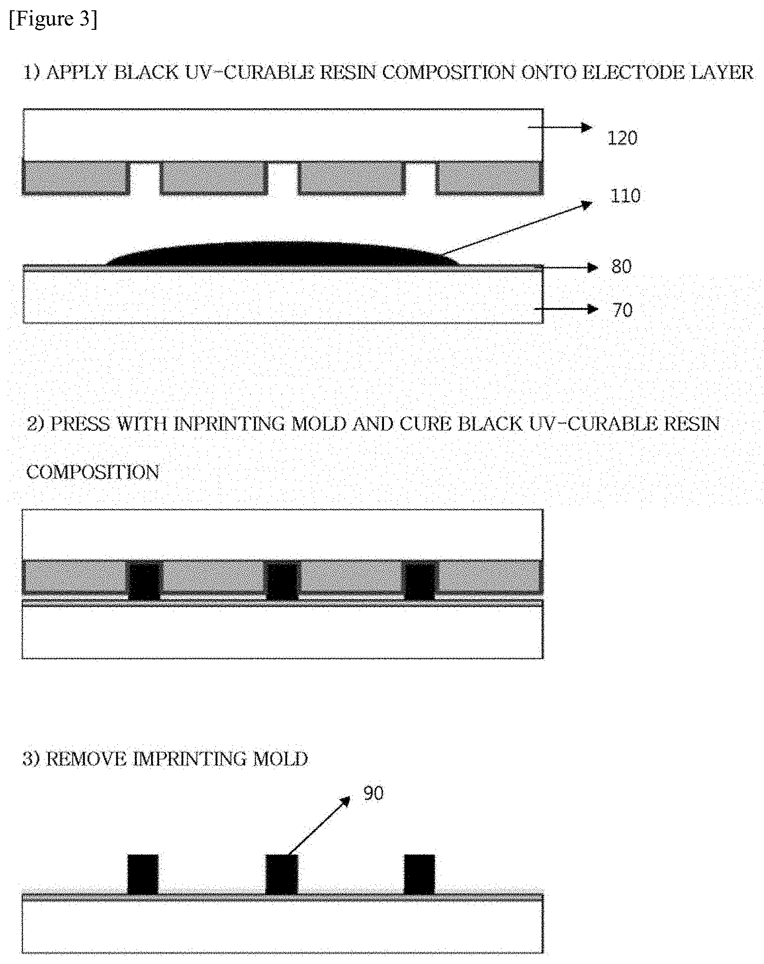
| Current CPC Class: | G02F 1/167 20130101; G03F 7/028 20130101; G03F 7/0002 20130101 |
| International Class: | G02F 1/167 20060101 G02F001/167; G03F 7/00 20060101 G03F007/00; G03F 7/028 20060101 G03F007/028 |
Foreign Application Data
| Date | Code | Application Number |
|---|---|---|
| Mar 27, 2018 | KR | 10-2018-0034975 |
Claims
1. A black partition wall pattern film comprising: a transparent substrate; an electrode layer provided on the transparent substrate; a black partition wall pattern provided on the electrode layer; and a black UV-curable resin layer provided in a region on the electrode layer where no black partition wall pattern is provided.
2. The black partition wall pattern film of claim 1, wherein a line height of the black partition wall pattern is 5 .mu.m or more.
3. The black partition wall pattern film of claim 1, wherein a line width of the black partition wall pattern is 30 .mu.m or less.
4. The black partition wall pattern film of claim 1, wherein a transmittance of the black partition wall pattern is 5% or less.
5. The black partition wall pattern film of claim 1, wherein a thickness of the black UV-curable resin layer is 1 .mu.m or less.
6. The black partition wall pattern film of claim 1, wherein a transmittance of the black UV-curable resin layer is 80% or more.
7. The black partition wall pattern film of claim 1, wherein the black partition wall pattern and the black UV-curable resin layer each separately comprises one or more of an acrylic monomer, an acrylic oligomer, a photoinitiator, a black pigment, and a black dye.
8. The black partition wall pattern film of claim 1, wherein the electrode layer comprises a transparent conductive oxide.
9. The black partition wall pattern film of claim 8, wherein the transparent conductive oxide comprises one or more of an indium oxide, a zinc oxide, an indium tin oxide, an indium zinc oxide, and an indium zinc tin oxide.
10. A method of manufacturing the black partition wall pattern film of claim 1, the method comprising: forming an electrode layer on a transparent substrate; applying a black UV-curable resin composition onto the electrode layer; pressing the applied black UV-curable resin composition with an imprinting mold and then curing the black UV-curable resin composition; and removing the imprinting mold.
11. A variable transmittance film comprising the black partition wall pattern film of claim 1.
12. The variable transmittance film of claim 11, wherein the variable transmittance film comprises charged nanoparticles responsive to electrophoresis during which a voltage is applied.
Description
CROSS-REFERENCE TO RELATED APPLICATIONS
[0001] This application is a National Stage Application of International Application No. PCT/KR2019/002784 filed on Mar. 11, 2019, which claims priority to and the benefit of Korean Patent Application No. 10-2018-0034975 filed with the Korean Intellectual Property Office on Mar. 27, 2018, the entire contents of which are incorporated herein by reference.
TECHNICAL FIELD
[0002] The present application relates to a black partition wall pattern film and a method of manufacturing the same.
BACKGROUND
[0003] An electrophoretic variable transmittance film is easy to transmit and block light entering from outside and thus can be used as a smart window for a building, a sunroof for a vehicle, and a light blocking film for a transparent display.
[0004] FIG. 1 is a view illustrating an operating principle of an electrophoretic variable transmittance film in the related art which operates in a light blocking mode or a light transmitting mode.
[0005] In general, as illustrated in FIG. 1, in order to switch from the light blocking mode to the light transmitting mode, a positive voltage is applied to a metal electrode pattern, and negatively charged nanoparticles are concentrated on the metal electrode pattern having a relatively small electrode width, such that the light blocking mode can be converted into the light transmitting mode.
[0006] However, there is a problem in that visibility is increased because of ball spacers used to maintain a distance between the metal electrode pattern and a transparent substrate in the electrophoretic variable transmittance film.
BRIEF DESCRIPTION
Technical Problem
[0007] The present application has been made in an effort to provide a black partition wall pattern film and a method of manufacturing the same.
Technical Solution
[0008] An exemplary embodiment of the present application provides a black partition wall pattern film comprising:
[0009] a transparent substrate;
[0010] an electrode layer provided on the transparent substrate;
[0011] a black partition wall pattern provided on the electrode layer; and
[0012] a black UV-curable resin layer provided in a region on the electrode layer where no black partition wall pattern is provided.
[0013] Provided is a black partition pattern film including the same.
[0014] In addition, another exemplary embodiment of the present application provides a method of manufacturing the black partition wall pattern film, the method comprising:
[0015] forming an electrode layer on a transparent substrate;
[0016] applying a black UV-curable resin composition onto the electrode layer;
[0017] pressing the applied black UV-curable resin composition with an imprinting mold and then curing the black UV-curable resin composition; and
[0018] removing the imprinting mold.
[0019] The present invention provides a method for manufacturing the black partition wall pattern film including the black partition wall pattern film.
[0020] In addition, still another exemplary embodiment of the present application provides a variable transmittance film comprising the black partition wall pattern film.
Advantageous Effects
[0021] According to the exemplary embodiment of the present application, since the black partition wall pattern is comprised, it is possible to prevent the transmittance from increasing in the light blocking mode when the exemplary embodiment is applied to an electrophoretic smart window.
[0022] In addition, according to the exemplary embodiment of the present application, since the black partition wall pattern film can be manufactured by using the imprinting process, it is possible to simplify the process of manufacturing the black partition wall pattern film and to form the black partition wall pattern having a desired line width.
BRIEF DESCRIPTION OF DRAWINGS
[0023] FIG. 1 is a view schematically illustrating a variable transmittance film in the related art.
[0024] FIG. 2 is a view schematically illustrating a black partition wall pattern film according to an exemplary embodiment of the present application.
[0025] FIG. 3 is a view schematically illustrating a method of manufacturing the black partition wall pattern film according to the exemplary embodiment of the present application.
[0026] FIG. 4 is a view schematically illustrating a method of manufacturing an imprinting mold according to the exemplary embodiment of the present application.
[0027] FIG. 5 is a view illustrating a microscopic image, in a light transmitting mode, of the black partition wall pattern film according to the exemplary embodiment of the present application.
[0028] FIG. 6 is a view illustrating an SEM image of the black partition wall pattern film according to the exemplary embodiment of the present application.
DESCRIPTION OF REFERENCE NUMERALS
[0029] 10: First transparent substrate
[0030] 20: Second transparent substrate
[0031] 30: First electrode layer
[0032] 40: Second electrode pattern
[0033] 50: Negatively (-) charged carbon black nanoparticle
[0034] 60: Ball spacer
[0035] 70: Transparent substrate
[0036] 80: Electrode layer
[0037] 90: Black partition wall pattern
[0038] 100: Black UV-curable resin layer
[0039] 110: Black UV-curable resin composition
[0040] 120: Imprinting mold
[0041] 130: Transparent base
[0042] 140: Dry film resist
[0043] 150: Release layer
DETAILED DESCRIPTION
[0044] Hereinafter, the present application will be described in detail.
[0045] In the present application, the term "transparent" means that transmittance is about 80% or higher in a visible ray region (400 nm to 700 nm).
[0046] Typically, it is essential to use a transparent electrode film and a metal pattern electrode film in order to manufacture an electrophoretic variable transmittance film. In addition, a cell gap needs to be maintained in order to inject an electrophoretic substance such as a negatively (-) charged carbon black particle dispersed solution between the two electrode films. To this end, a ball spacer, a column spacer pattern, or a partition wall pattern needs to be provided. A variable transmittance film in the related art is schematically illustrated in FIG. 1.
[0047] In a case in which a photolithography process using a photosensitive resin composition is applied to manufacture the partition wall pattern, there is a limitation in implementing a partition wall pattern having a uniform line width in a large area. This is due to uniformity of an exposure gap of a photomask and a photosensitive resin composition layer and uniformity of application of the photosensitive resin composition layer.
[0048] In addition, in a case in which a transparent partition wall pattern is applied to manufacture the partition wall pattern, there can be a problem in that transmittance is increased in a light blocking mode when the exemplary embodiment is applied to a smart window. This problem can be caused by a leakage of light at the transparent partition wall pattern.
[0049] In addition, in a case in which the photolithography process is used to manufacture a black partition wall pattern, exposure energy is not transferred to a lower side due to high optical density of a black photosensitive resin composition, and as a result, the partition wall pattern may not be implemented. In addition, in a case in which the exposure energy is excessively emitted in order to solve the problems, there can be a problem in that a line width of the partition wall pattern is greatly increased.
[0050] Therefore, the present application provides a black partition wall pattern film and a method of manufacturing the same which are capable of solving the above-mentioned problems.
[0051] A black partition wall pattern film according to an exemplary embodiment of the present application comprises: a transparent substrate; an electrode layer provided on the transparent substrate; a black partition wall pattern provided on the electrode layer; and a black UV-curable resin layer provided in a region on the electrode layer where no black partition wall pattern is provided.
[0052] In the present application, the transparent substrate can be, but not limited to, a glass base or a transparent plastic base which is excellent in transparency, surface smoothness, tractability, and waterproofness, and the transparent base is not limited as long as the transparent base is typically used for electronic elements. Specifically, the transparent base can be made of glass, urethane resin, polyimide resin, polyester resin, (meth)acrylate-based polymeric resin, or polyolefin-based resin such as polyethylene or polypropylene.
[0053] In the present application, the electrode layer can comprise a transparent conductive oxide. More specifically, the electrode layer can comprise, but is not limited only to, one or more of an indium oxide, a zinc oxide, an indium tin oxide, an indium zinc oxide, and an indium zinc tin oxide.
[0054] In order to ensure a redispersion property of charged particles when the light blocking mode is activated, surface resistance of the electrode layer can be 200 .OMEGA./sq. or less.
[0055] In the present application, a line height of the black partition wall pattern can be 5 .mu.m or more, and a line width of the black partition wall pattern can be 30 .mu.m or less. In addition, a line height of the black partition wall pattern can be 5 .mu.m to 50 and a line width of the black partition wall pattern can be 5 .mu.m to 30 .mu.m. If the line height of the black partition wall pattern is less than 5 .mu.m, a distance between a transparent electrode and a metal electrode pattern substrate is decreased, such that the content of negatively (-) charged nanoparticles in a dispersion liquid is excessively increased in order to ensure the transmittance of 1% or less in the light blocking mode, and as a result, there can be a problem in that a dispersion property of the negatively (-) charged nanoparticles deteriorates when a variable transmittance element operates. In addition, if the line height of the black partition wall pattern is more than 50 .mu.m, the distance between the transparent electrode and the metal electrode pattern substrate is increased, and as a result, an operating speed can be decreased. A cell gap between the electrodes can be determined based on the line height of the black partition wall pattern. More specifically, if the cell gap is small, concentration of a light blocking dispersion liquid can be increased in order to ensure a light blocking property, and an excessive increase in concentration of charged particles can degrade dispersion stability. In addition, if the cell gap is large, intensity of an electric field formed between the transparent electrode and the metal pattern can be decreased, and an electrophoretic property, that is, a movement speed of particles can be decreased as the distance between the charged particles and the metal pattern is increased.
[0056] The transmittance of the black partition wall pattern can be 5% or less. In addition, the transmittance of the black partition wall pattern can be 0 to 5%. If the transmittance of the black partition wall pattern is more than 5%, there can be a problem in that the black partition wall pattern is visible in the light blocking mode. In the case of an electrophoretic variable transmittance film which is currently under development, the transmittance in the light blocking mode (a state in which a light blocking dispersion liquid is dispersed) is at a level of 1% to 5%. If the transmittance of the black partition wall pattern is higher than this level, a leakage of light can be visible at a partition wall part.
[0057] A line spacing of the black partition wall pattern can be 100 .mu.m to 1,000 .mu.m. If the line spacing of the black partition wall pattern is less than 100 .mu.m, a range of variable transmittance can be decreased due to an increase in area of a region of the partition wall pattern. If the line spacing of the black partition wall pattern is more than 1,000 .mu.m, it can be difficult to maintain a uniform cell gap of the electrophoretic element. There is no variable transmittance in a region in which the black partition wall pattern is present, and as a result, an area of the variable transmittance region is decreased if the line spacing of the black partition wall pattern is too small when the line width remains the same. In contrast, if the line spacing is too large, a substrate (film) is deformed during a process of laminating a transparent electrode substrate and a metal pattern substrate, and as a result, bubbles can be produced, and uniformity of the cell gap can deteriorate.
[0058] In the present application, a black UV-curable resin layer having a thickness equal to the line height of the black partition wall pattern is formed on an entire surface of a glass substrate, and then the transmittance can be measured by using a spectrophotometer (SolidSpec-3700, Shimadzu Corp.).
[0059] In the present application, a thickness of the black UV-curable resin layer can be 1 .mu.m or less, and transmittance of the black UV-curable resin layer can be 80% or more. In addition, the thickness of the black UV-curable resin layer can be more than 0 and 1 .mu.m or less, and the transmittance of the black UV-curable resin layer can be 80% or more and less than 100%. If the thickness of the black UV-curable resin layer is more than 1 .mu.m, the formation of the electric field between the transparent electrode and the metal electrode pattern is hindered, and as a result, there can be a problem in that an operating property of the electrophoretic element can deteriorate. In addition, if the transmittance of the black UV-curable resin layer is less than 80%, the transmittance is decreased in a light transmitting mode, and as a result, there can be a problem in that a variable transmittance range of the electrophoretic element is decreased.
[0060] In the present application, the black partition wall pattern and the black UV-curable resin layer each can be made of a black UV-curable resin composition, and the black UV-curable resin composition can comprise, but is not limited only to, one or more of an acrylic monomer, an acrylic oligomer, a photoinitiator, a black pigment, and a black dye.
[0061] In the present application, the black partition wall pattern and the black UV-curable resin layer can be simultaneously formed by applying the black UV-curable resin composition onto the electrode layer and then performing an imprinting process. That is, the black partition wall pattern and the black UV-curable resin layer can comprise the same material.
[0062] The black partition wall pattern film according to the exemplary embodiment of the present application is schematically illustrated in FIG. 2. As illustrated in FIG. 2, the black partition wall pattern film according to the exemplary embodiment of the present application comprises: a transparent substrate 70; an electrode layer 80 provided on the transparent substrate 70; a black partition wall pattern 90 provided on the electrode layer 80; and a black UV-curable resin layer 100 provided in a region on the electrode layer 80 where no black partition wall pattern 90 is provided.
[0063] In addition, a method of manufacturing the black partition wall pattern film according to the exemplary embodiment of the present application comprises: forming an electrode layer on a transparent substrate; applying a black UV-curable resin composition on the electrode layer; pressing the applied black UV-curable resin composition with an imprinting mold and then curing the black UV-curable resin composition; and removing the imprinting mold.
[0064] The method of manufacturing the black partition wall pattern film according to the exemplary embodiment of the present application is schematically illustrated in FIG. 3. As illustrated in FIG. 3, the method of manufacturing the black partition wall pattern film according to the exemplary embodiment of the present application comprises: forming the electrode layer 80 on the transparent substrate 70; applying a black UV-curable resin composition 110 onto the electrode layer 80; pressing the applied black UV-curable resin composition 110 with an imprinting mold 120 and then curing the black UV-curable resin composition 110; and removing the imprinting mold 120.
[0065] In the present application, the forming of the electrode layer on the transparent substrate can use a method known in this technical field. More specifically, the forming of the electrode layer on the transparent substrate can use, but is not limited only to, a deposition process or the like.
[0066] A method of manufacturing the imprinting mold according to the exemplary embodiment of the present application is schematically illustrated in FIG. 4. More specifically, the imprinting mold can be manufactured by a manufacturing method comprising, but not limited only to, forming a dry film resist 140 on a transparent base 130; forming a pattern by exposing and developing the dry film resist 140; and forming a release layer 150 on the transparent base and the pattern.
[0067] The release layer can be implemented as a layer with a mixture of fluorine-based and silicone-based release materials. A thickness of the release layer can be, but is not limited only to, 100 nm or less. Examples of a method of forming the release layer comprise a wet coating method, a vapor deposition method, and the like, and the vapor deposition method is advantageous in implementing a uniform release layer on a surface having a stepped portion.
[0068] In addition, the exemplary embodiment of the present application provides a variable transmittance film comprising the black partition wall pattern film.
[0069] The variable transmittance film according to the exemplary embodiment of the present application can be formed by using a material and a method which are known in this technical field, except that the variable transmittance film comprises the black partition wall pattern film.
[0070] For example, the variable transmittance film can have a second transparent substrate having a second electrode pattern provided on the black partition wall pattern film. Negatively (-) charged nanoparticles are comprised between the electrode layer and the second electrode pattern of the black partition wall pattern film.
[0071] The negatively (-) charged nanoparticle can be, but is not limited only to, a carbon black nanoparticle.
[0072] The variable transmittance film can be manufactured by using, but is not limited only to, a method of preparing the above-mentioned variable transmittance film, and then injecting a solution, in which the negatively (-) charged nanoparticles are dispersed, between the electrode layer and the second electrode pattern of the black partition wall pattern film.
[0073] In the present application, the variable transmittance film can be operated by electrophoresis. The transmittance is decreased when the variable transmittance film according to the exemplary embodiment of the present application is in an OFF mode. The transmittance can be increased as the negatively (-) charged nanoparticles are concentrated on the metal pattern, which is a positive (+) electrode, due to the electrophoresis in an ON mode in which a voltage is applied to the electrode layer and the second electrode pattern.
Exemplary Embodiments
[0074] Hereinafter, the exemplary embodiment disclosed in the present specification will be described with reference to examples. However, the scope of the exemplary embodiment is not intended to be limited by the following examples.
EXAMPLES
Example 1
[0075] 1) Manufacture of Imprinting Mold
[0076] A dry film resist (DFR) having a thickness of 25 .mu.m was roll-laminated on a transparent PET film of 250 .mu.m under a condition in which a temperature was 110.degree. C., a rate was 1.3 mpm (meter per min), and a pressure was 0.4 MPa. Exposure energy of 150 mJ/cm.sup.2 was selectively applied by using an exposure device using parallel light with a wavelength of 365 nm (photo process). A DFR pattern film having a debossed portion with a line width of 25 .mu.m and a depth of 25 .mu.m was manufactured by spray-developing the completely exposed DFR laminated film for 90 seconds by using a developer having Na.sub.2CO.sub.3 of 1 wt. % under a condition in which a temperature was 30.degree. C. and a spray pressure was 0.2 MPa.
[0077] An imprinting mold was completely manufactured by forming a release layer having a thickness of 100 nm and having a mixture of fluorine-based and silicone-based release materials on the DFR pattern film by using a vapor deposition method.
[0078] 2) Manufacture of Transparent UV-Curable Resin Composition
[0079] A transparent UV-curable resin composition was manufactured with compositions shown in Table 1.
TABLE-US-00001 TABLE 1 Content Product Name Manufacturer (wt. %) CN9010 NS Sartomer 28.5 (alicyclic urethane acrylate monomer) CN8004 Sartomer 28.5 (alicyclic urethane acrylate monomer) SR444NS Sartomer 38 (pentaerythritol triacrylate) Irgacure 184 Ciba 4 (photoinitiator) SR9051 Sartomer 1 (attachment force enhancer) Total 100
[0080] 3) Manufacture of Black UV-Curable Resin Composition
[0081] A black UV-curable resin composition was manufactured by mixing a black mill base of 20 parts by weight (carbon black of 20 parts by weight having a particle diameter of 100 nm, a dispersing agent of 4 parts by weight, and trimethylol propane triacrylate of 76 parts by weight) with the transparent UV-curable resin composition of 80 parts by weight.
[0082] 4) Manufacture of Black Partition Wall Pattern Film
[0083] The black UV-curable resin composition was applied onto an ITO film having surface resistance of 150 .OMEGA./sq., and then roll-pressed with the imprinting mold with a pressure of 0.5 MPa and a rate of 0.1 mpm. The ITO film having a black partition wall pattern was manufactured by irradiating the laminate, from above thereof, with exposure energy of 1 J/cm.sup.2 by using a UV curing device with a wavelength of 365 nm and then separating the imprinting mold from the ITO film.
[0084] The black partition wall pattern manufactured by the imprinting process had a line width of 25 .mu.m and a line height of 25 .mu.m. A thickness of the black UV-curable resin layer in a region in which no black partition wall pattern is provided was 0.5 .mu.m.
[0085] The transmittance of the black partition wall pattern was 3%, and the transmittance of the black UV-curable resin layer having no black partition wall pattern was 92%.
[0086] A black UV-curable resin layer having a thickness equal to a line height of the black partition wall pattern or the black UV-curable resin layer was formed on an entire surface of a glass substrate, and then the transmittance was measured by using a spectrophotometer (SolidSpec-3700, Shimadzu Corp.).
[0087] A microscopic image, in the light transmitting mode, of the black partition wall pattern film according to Example 1 is illustrated in FIG. 5, and an SEM image of the black partition wall pattern film is illustrated in FIG. 6.
Comparative Example 1
[0088] A transparent UV-curable resin was applied onto an ITO film having surface resistance of 150 .OMEGA./sq., and then roll-pressed with the imprinting mold with a pressure of 0.5 MPa and at a rate of 0.1 mpm. The ITO film having a transparent partition wall pattern was manufactured by irradiating the laminate, from above thereof, with exposure energy of 1 J/cm.sup.2 by using a UV curing device with a wavelength of 365 nm and then separating the imprinting mold from the ITO film.
[0089] The transparent partition wall pattern manufactured by the imprinting process had a line width of 25 .mu.m and a line height of 25 .mu.m. A thickness of the transparent UV-curable resin layer in a region in which no transparent partition wall pattern is provided was 0.5 .mu.m.
[0090] The transmittance of the transparent partition wall pattern was 85%, and the transmittance of the transparent UV-curable resin layer having no transparent partition wall pattern was 95%.
[0091] As a result, according to the exemplary embodiment of the present application, since the black partition wall pattern is present, it is possible to prevent the transmittance from increasing in the light blocking mode when the exemplary embodiment is applied to an electrophoretic smart window.
[0092] In addition, according to the exemplary embodiment of the present application, since the black partition wall pattern film can be manufactured by using the imprinting process, it is possible to simplify the process of manufacturing the black partition wall pattern film and to form the black partition wall pattern having a desired line width.
* * * * *
D00000
D00001
D00002
D00003
D00004
XML
uspto.report is an independent third-party trademark research tool that is not affiliated, endorsed, or sponsored by the United States Patent and Trademark Office (USPTO) or any other governmental organization. The information provided by uspto.report is based on publicly available data at the time of writing and is intended for informational purposes only.
While we strive to provide accurate and up-to-date information, we do not guarantee the accuracy, completeness, reliability, or suitability of the information displayed on this site. The use of this site is at your own risk. Any reliance you place on such information is therefore strictly at your own risk.
All official trademark data, including owner information, should be verified by visiting the official USPTO website at www.uspto.gov. This site is not intended to replace professional legal advice and should not be used as a substitute for consulting with a legal professional who is knowledgeable about trademark law.