Organic Thin Film Transistor, And Fabricating Method Thereof
CHENG; Leilei
U.S. patent application number 16/866446 was filed with the patent office on 2020-08-20 for organic thin film transistor, and fabricating method thereof. The applicant listed for this patent is BOE TECHNOLOGY GROUP CO., LTD.. Invention is credited to Leilei CHENG.
| Application Number | 20200266353 16/866446 |
| Document ID | 20200266353 / US20200266353 |
| Family ID | 1000004811272 |
| Filed Date | 2020-08-20 |
| Patent Application | download [pdf] |


| United States Patent Application | 20200266353 |
| Kind Code | A1 |
| CHENG; Leilei | August 20, 2020 |
ORGANIC THIN FILM TRANSISTOR, AND FABRICATING METHOD THEREOF
Abstract
An organic thin film transistor includes a transparent base substrate and a transparent gate layer formed on the transparent base substrate. A gate insulating layer includes an oxidized inorganic sub-layer and a non-oxidized organic sub-layer formed on the transparent gate layer. A source electrode and a drain electrode are buried within the non-oxidized organic sub-layer. Each of the source electrode and the drain electrode has a bottom side, and the bottom side surface of each of the source electrode and the drain electrode faces the transparent gate layer and contacts the non-oxidized organic sub-layer. The transparent gate layer is buried within the oxidized inorganic sub-layer, and the oxidized inorganic sub-layer covers a top surface and side surfaces of the transparent gate layer.
| Inventors: | CHENG; Leilei; (Beijing, CN) | ||||||||||
| Applicant: |
|
||||||||||
|---|---|---|---|---|---|---|---|---|---|---|---|
| Family ID: | 1000004811272 | ||||||||||
| Appl. No.: | 16/866446 | ||||||||||
| Filed: | May 4, 2020 |
Related U.S. Patent Documents
| Application Number | Filing Date | Patent Number | ||
|---|---|---|---|---|
| 15501286 | Feb 2, 2017 | |||
| PCT/CN2016/095305 | Aug 15, 2016 | |||
| 16866446 | ||||
| Current U.S. Class: | 1/1 |
| Current CPC Class: | H01L 51/0545 20130101; H01L 51/0001 20130101; H01L 51/0533 20130101; H01L 51/055 20130101; H01L 51/0036 20130101 |
| International Class: | H01L 51/00 20060101 H01L051/00; H01L 51/05 20060101 H01L051/05 |
Foreign Application Data
| Date | Code | Application Number |
|---|---|---|
| Jan 29, 2016 | CN | 201610066532.4 |
Claims
1. An organic thin film transistor, comprising: a transparent base substrate; a transparent gate layer formed on the transparent base substrate; a gate insulating layer including an oxidized inorganic sub-layer and a non-oxidized organic sub-layer on the transparent gate layer; and a source electrode and a drain electrode buried within the non-oxidized organic sub-layer, each of the source electrode and the drain electrode having a bottom side, and the bottom side surface of each of the source electrode and the drain electrode facing the transparent gate layer and contacting the non-oxidized organic sub-layer, wherein the transparent gate layer is buried within the oxidized inorganic sub-layer, and the oxidized inorganic sub-layer covers a top surface and side surfaces of the transparent gate layer.
2. The organic thin film transistor of claim 1, wherein the transparent gate layer and the transparent base substrate are transparent to ultraviolet light.
3. The organic thin film transistor of claim 1, wherein the oxidized inorganic sub-layer includes a portion of a first initial silicone polymer layer, the portion of the first initial silicone polymer layer being oxidized.
4. The organic thin film transistor of claim 3, wherein the first initial silicone polymer layer includes a polydimethylsiloxane film or a derivative of polydimethylsiloxane film.
5. The organic thin film transistor of claim 3, wherein the first initial silicone polymer layer includes a polydimethylsiloxane film or a hydroxylated polydimethylsiloxane film.
6. The organic thin film transistor of claim 3, wherein the oxidized inorganic sub-layer includes SiO.sub.2 and the non-oxidized organic sub-layer includes the first initial silicone polymer.
7. The organic thin film transistor of claim 1, further comprising a recessed part formed on the gate insulating layer, wherein the source electrode and the drain electrode are buried within the non-oxidized organic sub-layer in the recessed part.
8. The organic thin film transistor of claim 7, wherein a surface energy reducing solution is coated on a portion of the gate insulating layer other than the recessed part.
9. The organic thin film transistor of claim 8, wherein the surface energy reducing solution on the portion of the gate insulating layer other than the recessed part is identical to a surface energy reducing solution coated on a carrying substrate.
10. The organic thin film transistor of claim 1, further comprising an organic semiconductor layer that contacts with both the source electrode and the drain electrode as an active layer, wherein a material of the active layer includes one of polythiophene, polyaniline, polypyrrole, polyfluorene, pentacene, and titanyl phthalocyanine.
11. The organic thin film transistor of claim 1, wherein the source electrode and the drain electrode include a metal material extracted from a hydrophilic solvent.
12. The organic thin film transistor of claim 11, wherein: the metal material includes one of gold, aluminum, chromium, titanium, nickel, molybdenum, and an alloy thereof, and the hydrophilic solvent includes an ethanol solvent.
13. The organic thin film transistor of claim 8, wherein: a material of the transparent gate layer includes one of indium tin oxide, indium zinc oxide, and graphene, and the surface energy reducing solution includes a hexamethyldisilazane solution or an octadecyltrichlorosilane solution.
14. The organic thin film transistor of claim 10, further comprising a protecting layer that includes an oxidized inorganic protecting sub-layer and a non-oxidized organic protecting sub-layer on the active layer, wherein the oxidized inorganic protecting layer includes a portion of a second initial silicone polymer layer, the portion of the second initial silicone polymer layer being oxidized.
15. The organic thin film transistor of claim 14, wherein the oxidized inorganic protecting sub-layer includes SiO.sub.2 and the non-oxidized organic protecting sub-layer contacts the active layer.
16. The organic thin film transistor of claim 14, wherein the active layer is buried within the non-oxidized organic protecting sub-layer.
17. The organic thin film transistor of claim 14, wherein the second initial silicone polymer layer includes a polydimethylsiloxane film or a derivative of polydimethylsiloxane film.
18. The organic thin film transistor of claim 3, wherein: the first initial silicone polymer layer includes a polydimethylsiloxane film or a derivative of polydimethylsiloxane film, the oxidized inorganic sub-layer includes SiO.sub.2, and the non-oxidized organic sub-layer includes a polydimethylsiloxane film or a derivative of polydimethylsiloxane film.
19. The organic thin film transistor of claim 14, wherein the protecting layer includes SiO.sub.2 and a polydimethylsiloxane film.
20. A semiconductor device, comprising the organic thin film transistor of claim 1.
Description
CROSS-REFERENCES TO RELATED APPLICATIONS
[0001] This application is a continuation of application Ser. No. 15/501,286, which is national phase entry under 35 U.S.C. .sctn. 371 of International Application No. PCT/CN2016/095305 filed on Aug. 15, 2016, claiming priority to Chinese Patent Application No. 201610066532.4 filed on Jan. 29, 2016, the entire contents of which are incorporated by reference herein.
TECHNICAL FIELD
[0002] The disclosed subject matter generally relates to display technologies and, more particularly, relates to an organic thin film transistor, and a fabricating method thereof.
BACKGROUND
[0003] The products of organic thin film transistor (OTFT) driven displays and electronic papers have been gradually entered into the market. An active layer of the OTFT is an organic active layer made by an organic semiconductor material.
[0004] The active layer may be made of small organic molecule and polymer semiconductor materials that have high migration rate, good solution processing ability, and stable environment providing ability. With the ongoing and in-depth study of the OTFT, it has been found that the carriers in the OTFT are conducted by a transition mode due to the existing of the intermolecular forces in the organic semiconductor materials. The organic semiconductors are being in a "molecular solid" form. Such special form can make the organic active layer made by an organic semiconductor be more susceptible by the insulating layer, resulting in significant changes in the carrier mobility, thus affecting the performances of the OTFT devices.
[0005] To solve the problem that the organic active layer made by an organic semiconductor is susceptible from the insulating layer and causes significant changes in the carrier mobility, an organic polymer material is usually used as the insulating layer of an OTFT. However, the dielectric constant of the organic polymer material is relatively low. When the organic polymer material is used alone as the insulating layer of an OTFT device, the threshold voltage of the OTFT device is relatively high, and the leakage current is relatively large.
[0006] Accordingly, it is desirable to provide an organic thin film transistor, and a fabricating method thereof to at least partially alleviate one or more problems set forth above and to solve other problems in the art.
BRIEF SUMMARY
[0007] In accordance with some embodiments of the disclosed subject matter, an organic thin film transistor, and a fabricating method thereof are provided.
[0008] One aspect of the disclosed subject matter provides a method for a method for forming an organic thin film transistor (OTFT), comprising: forming a transparent gate layer on a transparent base substrate; forming a first initial silicone polymer layer on the transparent gate layer; and performing an oxidization process to partially oxidize the first initial silicone polymer layer to form a gate insulating layer, including an oxidized inorganic sub-layer that contacts the transparent gate layer, and a non-oxidized organic sub-layer.
[0009] In some embodiments, forming a first initial silicone polymer layer on the transparent gate comprises: forming a polydimethylsiloxane film, or a derivative of polydimethylsiloxane film on the transparent gate.
[0010] In some embodiments, the derivative of polydimethylsiloxane film is a hydroxylated polydimethylsiloxane film.
[0011] In some embodiments, performing an oxidization process to partially oxidize the first initial silicone polymer layer comprises: performing an ultraviolet radiation treatment to partially oxidize the first initial silicone polymer layer to form the gate insulating layer, wherein the oxidized inorganic sub-layer is a SiO.sub.2 sub-layer, and the non-oxidized organic sub-layer is an initial silicone polymer sub-layer; and performing a low-temperature solidifying process to cure the gate insulating layer after performing the ultraviolet radiation treatment.
[0012] In some embodiments, the method further comprises: forming a recessed part on the gate insulating layer; and using a solution process to form a source electrode and a drain electrode in the recessed part.
[0013] In some embodiments, the method further comprises: before using a solution process forming the source electrode and the drain electrode in the recessed part, coating a surface energy reducing solution on the gate insulating layer other than the recessed part.
[0014] In some embodiments, coating a surface energy reducing solution on the gate insulating layer other than the recessed part comprises: overlying the transparent base substrate on a carrying substrate that is coated with a surface energy reducing solution, such that a portion of the gate insulating layer other than the recessed part contacts with the surface energy reducing solution coated on the carrying substrate; and removing the carrying substrate.
[0015] In some embodiments, the method further comprises: forming an organic semiconductor layer that contacts with both the source electrode and the drain electrode as an active layer.
[0016] In some embodiments, forming the source electrode and the drain electrode comprises: dispersing a metal material in a hydrophilic solvent to form a solution; and applying the solution into the recessed part; and evaporating the hydrophilic solvent of the solution to form the source electrode and the drain electrode by using a low-temperature solidifying process.
[0017] In some embodiments, the metal material is one of gold, aluminum, chromium, titanium, nickel, molybdenum, and an alloy thereof.
[0018] In some embodiments, wherein the hydrophilic solvent is an ethanol solvent.
[0019] In some embodiments, the recessed part is formed by using an imprinting lithography process.
[0020] In some embodiments, the surface energy reducing solution is a hexamethyldisilazane solution, or an octadecyltrichlorosilane solution.
[0021] In some embodiments, the method further comprises: a material of the active layer is one of polythiophene, polyaniline, polypyrrole, polyfluorene, pentacene, and titanyl phthalocyanine.
[0022] In some embodiments, a material of the transparent gate layer is one of indium tin oxide, indium zinc oxide, and graphene.
[0023] In some embodiments, the organic semiconductor layer is formed by using an ink-jet printing method.
[0024] In some embodiments, the method further comprises: forming a protecting layer on the active layer, including: forming a second initial silicone polymer layer on the active layer; performing an oxidization process to partially oxidize the second initial silicone polymer layer to form an oxidized inorganic protecting sub-layer and a non-oxidized organic protecting sub-layer.
[0025] In some embodiments, forming a protecting layer on the active layer further including: performing an ultraviolet radiation treatment to partially oxidize the second initial silicone polymer layer to form the protecting layer, wherein the oxidized inorganic protecting sub-layer is a SiO.sub.2 sub-layer, and the non-oxidized organic protecting sub-layer contacts the active layer; and performing a low-temperature solidifying process to cure the protecting layer after performing the ultraviolet radiation treatment.
[0026] In some embodiments, the second initial silicone polymer layer is a polydimethylsiloxane film, or a derivative of polydimethylsiloxane film.
[0027] In some embodiments, the first initial silicone polymer layer and the second initial silicone polymer layer are formed by using a coating process, or a spin coating process.
[0028] In some embodiments, the low-temperature solidifying process to the gate insulating layer is performed in a temperature range between 20.degree. C. to 60.degree. C.; and the low-temperature solidifying process to the protecting layer is performed in a temperature range between 20.degree. C. to 60.degree. C.
[0029] In some embodiments, the low-temperature solidifying process to the gate insulating layer has a duration between 4 hours to 8 hours; and the low-temperature solidifying process to the protecting layer has a duration between 4 hours to 8 hours.
[0030] Another aspect of the disclosed provided an organic thin film transistor, comprising: a transparent base substrate; a transparent gate layer on the base substrate; and a gate insulating layer formed by partially oxidizing a first initial silicone polymer layer on the transparent gate layer, wherein the gate insulating layer includes an oxidized inorganic sub-layer that contact the transparent gate layer, and a non-oxidized organic sub-layer on the oxidized organic sub-layer.
[0031] In some embodiments, the silicone polymer layer is a polydimethylsiloxane film or a derivative of polydimethylsiloxane layer; the oxidized inorganic sub-layer is a SiO.sub.2 film; and the non-oxidized organic sub-layer is a polydimethylsiloxane film or a derivative of polydimethylsiloxane film.
[0032] In some embodiments, the organic thin film transistor further comprises: a protecting layer formed by partially oxidizing a second initial silicone polymer layer.
[0033] In some embodiments, the protecting layer include a SiO.sub.2 film and a polydimethylsiloxane film, or the protecting layer include a SiO.sub.2 film and a derivative of polydimethylsiloxane film.
[0034] Other aspects of the disclosed subject matter can be understood by those skilled in the art in light of the description, the claims, and the drawings of the present disclosure.
BRIEF DESCRIPTION OF THE DRAWINGS
[0035] Various objects, features, and advantages of the disclosed subject matter can be more fully appreciated with reference to the following detailed description of the disclosed subject matter when considered in connection with the following drawings, in which like reference numerals identify like elements. It should be noted that the following drawings are merely examples for illustrative purposes according to various disclosed embodiments and are not intended to limit the scope of the present disclosure.
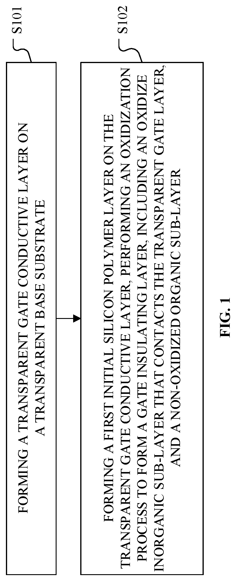
[0036] FIG. 1 is a flowchart of an exemplary method for fabricating an organic thin film transistor in accordance with some embodiments of the disclosed subject matter;
[0037] FIG. 2 is a flowchart of another exemplary method for fabricating an organic thin film transistor in accordance with some other embodiments of the disclosed subject matter;
[0038] FIG. 3 is a flowchart of another exemplary method for fabricating an organic thin film transistor in accordance with some other embodiments of the disclosed subject matter;
[0039] FIG. 4 is a schematic diagram of a first initial polydimethylsiloxane (PDMS) film of the organic thin film transistor formed on a gate layer in accordance with some embodiments of the disclosed subject matter;
[0040] FIG. 5 is a schematic structural diagram of a first SiO.sub.2 film of the organic thin film transistor formed by performing an ultraviolet treatment to the first initial PDMS film in accordance with some embodiments of the disclosed subject matter;
[0041] FIG. 6 is a schematic diagram of a source electrode and a drain electrode of the organic thin film transistor in accordance with some embodiments of the disclosed subject matter;
[0042] FIG. 7 is a schematic diagram of an active layer of the organic thin film transistor in accordance with some embodiments of the disclosed subject matter; and
[0043] FIG. 8 is a schematic structural diagram of a second initial PDMS film and a second SiO.sub.2 film of the organic thin film transistor formed on the active layer in accordance with some other embodiments of the disclosed subject matter.
DETAILED DESCRIPTION
[0044] For those skilled in the art to better understand the technical solution of the disclosed subject matter, reference will now be made in detail to exemplary embodiments of the disclosed subject matter, which are illustrated in the accompanying drawings. Wherever possible, the same reference numbers will be used throughout the drawings to refer to the same or like parts.
[0045] In accordance with various embodiments, the disclosed subject matter provides an organic thin film transistor, and a fabricating method thereof.
[0046] In the disclosed fabricating method for forming an organic thin film transistor (OTFT), a gate insulating layer can be formed on a substrate having a gate electrode, a drain electrode and an organic insulating layer can be formed on the gate insulating layer, and then a pattern of a protecting layer and pixel electrodes can be formed on the drain electrode and the organic insulating layer. By using a simple process to the organic polymers, an inorganic organic insulating layer can be formed to eliminate the defects of the gate insulating layer, to obtain a small leakage current, to reduce the hysteresis effect, and to improve the forming process of the insulating layer. The disclosed method further uses a solution process to form a source electrode and a drain electrode on the organic insulating layer to obtain a good ohmic contact with the organic semiconductor channel, thereby improving the response speed. The disclosed subject matter can replace the complex and unstable OTFT substrate preparation process, can improve the production efficiency, can reduce production costs, and can improve OTFT device performance.
[0047] Referring to FIG. 1, a flowchart of an exemplary method for fabricating an organic thin film transistor is shown in accordance with some embodiments of the disclosed subject matter. As illustrated, the method can include the following steps.
[0048] Step 101: forming a transparent gate layer on a transparent base substrate. For example, a base substrate can be transparent to ultraviolet light or ozone light.
[0049] In some embodiments, a material of the gate layer can be indium tin oxide (ITO), indium zinc oxide (IZO), graphene, or any other suitable material which an ultraviolet light can pass through.
[0050] Step 102: forming a first initial silicone polymer layer on the transparent gate layer, performing an oxidization process to partially oxidize the first initial silicone polymer layer to form a gate insulating layer, including an oxidized inorganic sub-layer that contacts the transparent gate layer, and a non-oxidized organic sub-layer.
[0051] In some embodiments, the first initial silicone polymer layer can be a polydimethylsiloxane (PDMS) film, or a derivative of polydimethylsiloxane film. The derivative of polydimethylsiloxane is PS-b-PDMS or hydroxylated polydimethylsiloxane.
[0052] In the following description, PDMS and ultraviolet (UV) light are used for example, A PDMS film can be formed on the transparent gate layer. An ultraviolet (UV) treatment can be performed on one surface of the first initial PDMS film facing the gate layer to form a first SiO.sub.2 film. Then a low-temperature solidifying process can be performed to cure the first SiO.sub.2 film and the remaining first initial PDMS film to form a gate insulating layer.
[0053] In some embodiments, the PDMS film can be replaced by any other suitable silicone polymer film, such as a polydimethylsiloxane (PDMS) film, or a polydimethylsiloxane derivative film, etc. The reason to use the hydroxylated polydimethylsiloxane (PDMS) film is that it has a hydrophilic nature.
[0054] A duration time and a temperature of the low-temperature solidifying process can be adjusted based on different product requirements. In some embodiments, a temperature of the low-temperature solidifying performed to the first SiO.sub.2 film and the first initial PDMS film can be in a range between 20.degree. C. and 60.degree. C., and a duration time of the low-temperature solidifying process can be in a range between 4 hours to about 8 hours, for example, about 6 hours.
[0055] In some embodiments, PDMS material is used for forming the gate insulating layer. PDMS is a silicone polymer having electrical insulating properties, and resistances to high temperature and low temperature. It can be used for a long term in an environment having a temperature from -50.degree. C. to 250.degree. C., Furthermore, PDMS has a large compression rate, a low surface tension, a good water repellency and a moisture resistance. Due to the low surface tension, a fluid form of the PDMS can easily form a smooth and uniform coating.
[0056] By using one surface of the first initial PDMS film facing the gate layer to form the first SiO.sub.2 film, a gate insulating layer can be formed including the SiO.sub.2 film and the first initial PDMS film. The SiO.sub.2 film and the first initial PDMS film can reduce the interfacial defects of the gate insulating layer. Thereby the fabricated OTFT can have a small leakage current which may reduce the hysteresis effect.
[0057] In such embodiments, by performing a UV treatment on one surface of the first initial PDMS film through the gate layer to form a first SiO.sub.2 film on the gate layer, the formed gate insulating layer can include the first SiO.sub.2 film and the first initial PDMS film. Thus the problems of high threshold voltage and large leakage current caused by using a single PDMS film as the gate insulating layer can be solved.
[0058] Turning to FIG. 2, a flowchart of another exemplary method for fabricating an organic thin film transistor is shown in accordance with some other embodiments of the disclosed subject matter. As illustrated, the method for fabricating an organic thin film transistor can include the followings steps.
[0059] In the following description, hydroxylated PDMS and ultraviolet (UV) light are used for example.
[0060] Step 201: forming a transparent gate layer on a base substrate that is transparent to an ultraviolet light.
[0061] Step 202: forming a first initial hydroxylated polydimethylsiloxane film on the gate layer, performing an ultraviolet (UV) treatment on one surface of the first initial hydroxylated PDMS film facing the gate layer to form a first SiO.sub.2 film, and low-temperature solidifying the first SiO.sub.2 film and the remaining first initial hydroxylated PDMS film to form a gate insulating layer.
[0062] Step 203: forming a recessed part on the gate insulating layer.
[0063] Preferably, the recessed part is formed by using an imprinting lithography process. In some embodiments, the recessed part is formed on a location that is to form a source electrode and a drain electrode.
[0064] Step 204: overlying the base substrate on a carrying substrate that is coated with a surface energy reducing solution.
[0065] After the overlying, the gate insulating layer of the base substrate faces the carrying substrate, a portion of the gate insulating layer other than the recessed part contacts with the surface energy reducing solution coated on the carrying substrate.
[0066] Preferably, the surface energy reducing solution is hexamethyldisilazane (HMDS) solution, or octadecyltrichlorosilane (OTS) solution.
[0067] Step 205: removing the carrying substrate, and forming a source electrode and a drain electrode in the recessed part on the gate insulating layer by using a solution process.
[0068] By using the solution process to form a source electrode and a drain electrode on an organic layer of the gate insulating layer, the source electrode and the drain electrode can have a good ohmic contact with an organic semiconductor layer that is to be formed in the subsequent step, thereby improving a response speed of the OTFT.
[0069] Specifically, forming a source electrode and a drain electrode in the recessed part on the gate insulating layer by using a solution process can include the following processes: dispersing a metal material in a hydrophilic solvent to form a solution; applying the solution into the recessed part; and evaporating the hydrophilic solvent of the solution to form the source electrode and the drain electrode by using a low-temperature solidifying process.
[0070] The metal material of the source electrode and the drain electrode can be dispersed uniformly in a hydrophilic solvent.
[0071] The hydrophilic solvent having uniformly dispersed metal material can be applied into the recessed part by using a coating method such as a spin coating method.
[0072] A low-temperature solidifying process can be performed to evaporate the hydrophilic solvent to form the source electrode and the drain electrode.
[0073] Step 206: forming an organic semiconductor layer that contacts with both the source electrode and the drain electrode as an active layer.
[0074] In some embodiments, the metal material of the source electrode and the drain electrode can be selected from gold, aluminum, chromium, titanium, nickel, molybdenum, etc., or any suitable alloy thereof. The hydrophilic solvent can be, for example, ethanol solvent.
[0075] The organic semiconductor layer can be formed by using an inkjet printing method. The material of the active layer can be a film of any one of the following materials: polythiophene (P3HT), polyaniline (PAE), polypyrrole, polyfluorene (Ph), pentacene, titanyl phthalocyanine (TiOPC), etc.
[0076] In such embodiments, by performing a UV treatment on one surface of the hydroxylated PDMS film facing the gate layer to form a first SiO.sub.2 film, the formed gate insulating layer can include the first SiO.sub.2 film and remaining hydroxylated PDMS film, Thus the problems of high threshold voltage and large leakage current caused by using a single PDMS film as the gate insulating layer can be solved. Further, by using a solution process to form a source electrode and a drain electrode on an organic layer of the gate insulating layer, the source electrode and the drain electrode can have a good ohmic contact with an organic semiconductor layer that is to be formed in the subsequent step, thereby improving a response speed of the OTFT.
[0077] Turning to FIG. 3, a flowchart of another exemplary method for fabricating an organic thin film transistor is shown in accordance with some other embodiments of the disclosed subject matter. As illustrated, the method or fabricating an organic thin film transistor can include the following steps.
[0078] In the following description, hydroxylated PDMS and ultraviolet (UV) light are used for example.
[0079] Step 301: forming a transparent gate layer on a base substrate that is transparent to an ultraviolet light.
[0080] In some embodiments, a material of the gate layer can be indium tin oxide (ITO), indium zinc oxide (IZO), graphene, or any other suitable material which an ultraviolet light can pass through.
[0081] Step 302: forming a first initial hydroxylated polydimethylsiloxane (PDMS) film on the gate layer, performing an ultraviolet (UV) treatment on one surface of the first initial hydroxylated PDMS film facing the gate layer to form a first SiO.sub.2 film, and low-temperature solidifying the first SiO.sub.2 film and the remaining first initial hydroxylated PDMS film to form a gate insulating layer.
[0082] A duration time and a temperature of the low-temperature solidifying process can be adjusted based on different product requirements. In some embodiments, a temperature of the low-temperature solidifying performed to the first SiO.sub.2 film and the first initial hydroxylated PDMS film can be in a range between 20.degree. C. and 60.degree. C., and a duration time of the low-temperature solidifying process can be in a range between 4 hours to about 8 hours, for example, about 6 hours.
[0083] In some embodiments, polydimethylsiloxane (PDMS) material is used for forming the gate insulating layer. PDMS is a silicone polymer having electrical insulating properties, and resistances to high temperature and low temperature. It can be used for a long term in an environment having a temperature from -50.degree. C. to 250.degree. C. Furthermore. PDMS has a large compression rate, a low surface tension, a good water repellency and a moisture resistance. Due to the low surface tension, a fluid form of the PDMS can easily form a smooth and uniform coating.
[0084] By oxidizing one surface of the first initial hydroxylated PDMS film facing the gate layer to form the first SiO.sub.2 film, a gate insulating layer can be formed including the SiO.sub.2 film and the remaining first initial hydroxylated PDMS film. The SiO.sub.2 film and the first initial hydroxylated PDMS film can reduce the interfacial defects of the gate insulating layer. Thereby the fabricated OTFT can have a small leakage current which may reduce the hysteresis effect.
[0085] Step 303: forming a recessed part of on the gate insulating layer.
[0086] Preferably, the recessed part is formed by using an imprinting lithography process.
[0087] Step 304: overlying the base substrate on a carrying substrate that is coated with a surface energy reducing solution. After the overlying, the gate insulating layer of the base substrate faces the carrying substrate, a portion of the gate insulating layer other than the recessed part contacts with the surface energy reducing solution coated on the carrying substrate.
[0088] Preferably, the surface energy reducing solution is hexamethyldisilazane (HMDS) solution, or octadecyltrichlorosilane (OTS) solution.
[0089] Step 305: removing the carrying substrate, and forming a source electrode and a drain electrode in the recessed part on the gate insulating layer by using a solution process.
[0090] By using the solution process to form a source electrode and a drain electrode on an organic layer of the gate insulating layer, the source electrode and the drain electrodes can have a good ohmic contact with an organic semiconductor layer that is to be formed in the subsequent step, thereby improving a response speed of the OTFT.
[0091] Specifically, forming a source electrode and a drain electrode in the recessed part on the gate insulating layer by using a solution process can include the following processes.
[0092] A metal material of the source electrode and the drain electrode can be dispersed uniformly in a hydrophilic solvent.
[0093] The hydrophilic solvent having uniformly dispersed metal material can be filled into the recessed part by using a coating method such as a spin coating method.
[0094] A low-temperature solidifying process can be performed to evaporate the hydrophilic solvent to form the source electrode and the drain electrode.
[0095] Step 306: forming an organic semiconductor layer that contacts with both the source electrode and the drain electrode as an active layer.
[0096] In some embodiments, the metal material of the source electrode and the drain electrode can be selected from gold, aluminum, chromium, titanium, nickel, molybdenum, etc., or any suitable alloy thereof. The hydrophilic solvent can be, for example, ethanol solvent.
[0097] The organic semiconductor layer can be formed by using an ink-jet printing method. The material of the active layer can be a film of any one of the following material: polythiophene (P3HT), polyaniline (PAE), polypyrrole, polyfluorene (PF), pentacene, titanyl phthalocyanine (TiOPC), etc.
[0098] Step 307: forming a second initial hydroxylated PDMS film on the active layer, performing an ultraviolet (UV) treatment on one surface of the second initial hydroxylated PDMS film facing the active layer to form a second SiO.sub.2 film, and low-temperature solidifying the second SiO.sub.2 film and the remaining second initial hydroxylated PDMS film to form a protecting layer.
[0099] The formation of gate insulating layer and the process of forming protecting; layer are the same.
[0100] In some embodiments, the second initial hydroxylated polydimethylsiloxane (PDMS) layer can be formed by using a coating method, or a spin coating method.
[0101] A duration time and a temperature of the low-temperature solidifying process can be adjusted based on different product requirements. In some embodiments, a temperature of the low-temperature solidifying performed to the second SiO.sub.2 film and the second initial hydroxylated PDMS film can be in a range between 20.degree. C. and 60.degree. C., and a duration time of the low-temperature solidifying process can be in a range between 4 hours to about 8 hours, for example, about 6 hours.
[0102] In such embodiments, by performing a UV treatment on one surface of the hydroxylated PDMS film facing the gate layer to form a first SiO.sub.2 film, the formed gate insulating layer can include the first SiO.sub.2 film and the remaining hydroxylated PDMS film. Thus the problems of high threshold voltage and large leakage current caused by, using a single PDMS film as the gate insulating layer can be solved.
[0103] Further, by using a solution process to form a source electrode and a drain electrode on an organic layer of the gate insulating layer, the source electrode and the drain electrode can have a good ohmic contact with an organic semiconductor layer that is to be formed in the subsequent step, thereby improving a response speed of the OTFT. Further, a stacking layer including a second SiO.sub.2 film and a second initial hydroxylated PDMS film can be formed on the active layer to protect the active layer.
[0104] In order to more clearly describe the disclosed subject matter, the method for forming the organic thin film transistor on certain stages are described below in connection with FIGS. 4-8.
[0105] Referring to FIG. 4, a schematic diagram of a first initial hydroxylated polydimethylsiloxane (PDMS) film of the organic thin film transistor formed on a gate layer is shown in accordance with some embodiments of the disclosed subject matter.
[0106] As illustrated, a gate layer 2 is formed on a base substrate 1, a first initial PDMS film 31 is formed on the gate layer 2. A material of the base substrate 1 can be transparent to an ultraviolet light. Similarly, a material of the gate layer 2 can also be transparent to an ultraviolet light. The material of the gate layer 2 can be selected from indium tin oxide (ITO) or indium zinc oxide (IZO).
[0107] In some embodiments, the first initial PDMS film 31 can be replaced by a first initial hydroxylated PDMS film 31.
[0108] Referring to FIG. 5, a schematic structural diagram of a first SiO.sub.2 film of the organic thin film transistor formed by performing an ultraviolet treatment to the first initial PDMS film is shown in accordance with some embodiments of the disclosed subject matter.
[0109] As illustrated, one surface of the first initial PDMS film 31 facing the gate layer 2 can be performed by an ultraviolet (UV) treatment and followed by a low-temperature solidifying process to convert the surface of the first initial PDMS film 31 into a first SiO.sub.2 film 32. The remaining first initial PDMS film 31 and the first SiO.sub.2 film 32 can constitute the gate insulating layer 3.
[0110] In some embodiments, a temperature of the low-temperature solidifying process can be in a range between 20.degree. C. and 60.degree. C., for example, about 40.degree. C., and a duration period of the low-temperature solidifying process can be in a range between 4 hours to about 8 hours, for example, about 6 hours.
[0111] Referring to FIG. 6, a schematic diagram of a source electrode and a drain electrode of the organic thin film transistor is shown in accordance with some embodiments of the disclosed subject matter.
[0112] As illustrated, a source electrode 4 and a drain electrode 5 can be formed on the gate insulating layer 3. An exemplary method for forming the source electrode 4 and the drain electrode 5 can be a solution process.
[0113] Referring to FIG. 7, a schematic diagram of an active layer of the organic thin film transistor is shown in accordance with some embodiments of the disclosed subject matter.
[0114] As illustrated, an active layer 6 can be formed on the source electrode 4 and the drain electrode 5.
[0115] It should be noted that, the structure shown in FIG. 7 can be regarded as an exemplary OTFT fabricated by all steps of the method described above in connection with FIG. 1, or as an exemplary OTFT fabricated by a portion of steps of the method described above in connection with FIG. 2.
[0116] It also should be noted that, a protecting layer 7 can also be formed on the active layer 6. A method for forming the protecting layer 7 can be similar to the process for forming the gate insulating layer 3. A difference is that the protecting layer 7 includes a second SiO.sub.2 film and a second PDMS film or a second hydroxylated PDMS film. The second SiO.sub.2 film is on one surface of the second PDMS film or the second hydroxylated PDMS film that faces away from the gate layer 2.
[0117] Referring to FIG. 8, a schematic structural diagram of a second initial hydroxylated PDMS film and a second SiO.sub.2 film of the organic thin film transistor formed on the active layer is shown in accordance with some other embodiments of the disclosed subject matter.
[0118] As illustrated, the organic thin film transistor can include the following components.
[0119] A transparent base substrate 1.
[0120] A transparent gate layer 2 on the transparent base substrate 1.
[0121] A gate insulating layer 3 including a first PDMS film or a first derivative of PDMS film 31 formed on the transparent gate layer 2, and a first SiO.sub.2 film formed from one surface of the first initial PDMS film or the first derivative of PDMS film 31 that faces the gate layer 2.
[0122] A source electrode 4 and a drain electrode 5 formed on the gate insulating layer 3.
[0123] An active layer 6 that is an organic semiconductor layer formed on and in directly contact with the source electrode 4 and the drain electrode 5.
[0124] In some embodiments, the organic thin film transistor further comprises a protecting layer 7 including a second PDMS film or a second derivative of PDMS (such as hydroxylated PDMS) film and a second SiO.sub.2 film on one surface of the second PDMS film or the second derivative of PDMS film that faces away from the gate layer 2.
[0125] The disclosed organic thin film transistor includes first SiO.sub.2 film formed by performing a UV treatment on one surface of a first initial PDMS layer or a first initial derivative of PDMS layer facing the gate layer. Thus a gate insulating layer of the disclosed organic thin film transistor can include the first SiO.sub.2 film and the first PDMS film or the first derivative of PDMS film. Therefore, the problems of high threshold voltage and large leakage current caused by using a single PDMS film or a single derivative of PDMS film as the gate insulating layer can be solved.
[0126] The provision of the examples described herein (as well as clauses phrased as "such as," "e.g.," "including," and the like) should not be interpreted as limiting the claimed subject matter to the specific examples; rather, the examples are intended to illustrate only some of many possible aspects.
[0127] Accordingly, an organic thin film transistor, and a fabricating method thereof are provided. The disclosed method can includes: forming a transparent gate layer on a transparent base substrate; forming a first initial silicone polymer layer on the transparent gate layer; and performing an oxidization process to partially oxidize the first initial silicone polymer layer to form a gate insulating layer, including an oxidized inorganic sub-layer that contacts the transparent gate layer, and a non-oxidized organic sub-layer.
[0128] In some embodiments, forming a first initial silicone polymer layer on the transparent gate comprises: forming a polydimethylsiloxane film, or a derivative of polydimethylsiloxane film on the transparent gate.
[0129] In some embodiments, the derivative of polydimethylsiloxane film is a hydroxylated polydimethylsiloxane film.
[0130] In some embodiments, performing an oxidization process to partially oxidize the first initial silicone polymer layer comprises: performing an ultraviolet radiation treatment to partially oxidize the first initial silicone polymer layer to form the gate insulating layer, wherein the oxidized inorganic sub-layer is a SiO.sub.2 sub-layer, and the non-oxidized organic sub-layer is an initial silicone polymer sub-layer; and performing a low-temperature solidifying process to cure the gate insulating layer after performing the ultraviolet radiation treatment.
[0131] In some embodiments, the method further comprises: forming a recessed part on the gate insulating layer; and using a solution process to form a source electrode and a drain electrode in the recessed part.
[0132] In some embodiments, the method further comprises: before using a solution process forming the source electrode and the drain electrode in the recessed part, coating a surface energy reducing solution on the gate insulating layer other than the recessed part.
[0133] In some embodiments, coating a surface energy reducing solution on the gate insulating layer other than the recessed part comprises: overlying the transparent base substrate on a carrying substrate that is coated with a surface energy reducing solution, such that a portion of the gate insulating layer other than the recessed part contacts with the surface energy reducing solution coated on the carrying substrate; and removing the carrying substrate.
[0134] In some embodiments, the method further comprises: forming an organic semiconductor layer that contacts with both the source electrode and the drain electrode as an active layer.
[0135] In some embodiments, forming the source electrode and the drain electrode comprises: dispersing a metal material in a hydrophilic solvent to form a solution; and applying the solution into the recessed part; and evaporating the hydrophilic solvent of the solution to form the source electrode and the drain electrode by using a low-temperature solidifying process.
[0136] In some embodiments, the metal material is one of gold, aluminum, chromium, titanium, nickel, molybdenum, and an alloy thereof.
[0137] In some embodiments, wherein the hydrophilic solvent is an ethanol solvent.
[0138] In some embodiments, the recessed part is formed by using an imprinting lithography process.
[0139] In some embodiments, the surface energy reducing solution is a hexamethyldisilazane solution, or an octadecyltrichlorosilane solution.
[0140] In some embodiments, the method further comprises: a material of the active layer is one of polythiophene, polyaniline, polypyrrole, polyfluorene, pentacene, and titanyl phthalocyanine.
[0141] In some embodiments, a material of the transparent gate layer is one of indium tin oxide, indium zinc oxide, and graphene.
[0142] In some embodiments, the organic semiconductor layer is formed by using an ink-jet printing method.
[0143] In some embodiments, the method further comprises: forming a protecting layer on the active layer, including: forming a second initial silicone polymer layer on the active layer; performing an oxidization process to partially oxidize the second initial silicone polymer layer to form an oxidized inorganic protecting sub-layer and a non-oxidized organic protecting sub-layer.
[0144] In some embodiments, forming a protecting layer on the active layer further including: performing an ultraviolet radiation treatment to partially oxidize the second initial silicone polymer layer to form the protecting layer, wherein the oxidized inorganic protecting sub-layer is a SiO.sub.2 sub-layer, and the non-oxidized organic protecting sub-layer contacts the active layer; and performing a low-temperature solidifying process to cure the protecting layer after performing the ultraviolet radiation treatment.
[0145] In some embodiments, the second initial silicone polymer layer is a polydimethylsiloxane film, or a derivative of polydimethylsiloxane film.
[0146] In some embodiments, the first initial silicone polymer layer and the second initial silicone polymer layer are formed by using a coating process, or a spin coating process.
[0147] In some embodiments, the low-temperature solidifying process to the gate insulating layer is performed in a temperature range between 20.degree. C. to 60.degree. C.; and the low-temperature solidifying process to the protecting layer is performed in a temperature range between 20.degree. C. to 60.degree. C.
[0148] In some embodiments, the low-temperature solidifying process to the gate insulating layer has a duration between 4 hours to 8 hours; and the low-temperature solidifying process to the protecting layer has a duration between 4 hours to 8 hours.
[0149] Another aspect of the disclosed provided an organic thin film transistor, comprising: a transparent base substrate; a transparent gate layer on the base substrate; and a gate insulating layer formed by partially oxidizing a first initial silicone polymer layer on the transparent gate layer, wherein the gate insulating layer includes an oxidized inorganic sub-layer that contact the transparent gate layer, and a non-oxidized organic sub-layer on the oxidized organic sub-layer.
[0150] In some embodiments, the silicone polymer layer is a polydimethylsiloxane film or a derivative of polydimethylsiloxane layer; the oxidized inorganic sub-layer is a SiO.sub.2 film; and the non-oxidized organic sub-layer is a polydimethylsiloxane film or a derivative of polydimethylsiloxane film.
[0151] In some embodiments, the organic thin film transistor further comprises: a protecting layer formed by partially oxidizing a second initial silicone polymer layer.
[0152] In some embodiments, the protecting layer include a SiO.sub.2 film and a polydimethylsiloxane film, or the protecting layer include a SiO.sub.2 film and a derivative of polydimethylsiloxane film.
[0153] Although the disclosed subject matter has been described and illustrated in the foregoing illustrative embodiments, it is understood that the present disclosure has been made only by way of example, and that numerous changes in the details of embodiment of the disclosed subject matter can be made without departing from the spirit and scope of the disclosed subject matter, which is only limited by the claims which follow. Features of the disclosed embodiments can be combined and rearranged in various ways. Without departing from the spirit and scope of the disclosed subject matter, modifications, equivalents, or improvements to the disclosed subject matter are understandable to those skilled in the art and are intended to be encompassed within the scope of the present disclosure.
* * * * *
D00000
D00001
D00002
D00003
D00004
D00005
XML
uspto.report is an independent third-party trademark research tool that is not affiliated, endorsed, or sponsored by the United States Patent and Trademark Office (USPTO) or any other governmental organization. The information provided by uspto.report is based on publicly available data at the time of writing and is intended for informational purposes only.
While we strive to provide accurate and up-to-date information, we do not guarantee the accuracy, completeness, reliability, or suitability of the information displayed on this site. The use of this site is at your own risk. Any reliance you place on such information is therefore strictly at your own risk.
All official trademark data, including owner information, should be verified by visiting the official USPTO website at www.uspto.gov. This site is not intended to replace professional legal advice and should not be used as a substitute for consulting with a legal professional who is knowledgeable about trademark law.