Zoom Lens Assembly
Boutte; Ronald Wayne ; et al.
U.S. patent application number 16/796080 was filed with the patent office on 2020-08-20 for zoom lens assembly. The applicant listed for this patent is MEMS OPTICAL ZOOM CORPORATION. Invention is credited to Ronald Wayne Boutte, Russell J. Kennett.
| Application Number | 20200264406 16/796080 |
| Document ID | 20200264406 / US20200264406 |
| Family ID | 1000004825636 |
| Filed Date | 2020-08-20 |
| Patent Application | download [pdf] |


View All Diagrams
| United States Patent Application | 20200264406 |
| Kind Code | A1 |
| Boutte; Ronald Wayne ; et al. | August 20, 2020 |
ZOOM LENS ASSEMBLY
Abstract
A zoom lens assembly may include lens elements, lens mounts, and an actuator. Each of the lens elements has an optical axis aligned to a common optical axis. At least one of the lens elements is a movable lens element and at least one of the lens elements is an aspheric lens element. Each of the lens elements has a lens diameter of 4 millimeters or less. The lens mounts are coupled to the lens elements and are configured to retain the lens elements in order. The actuator is coupled between the movable lens element and one of the lens mounts. The actuator is configured to selectively adjust an axial position of the movable lens element along the common optical axis. An optical zoom of the zoom lens assembly is at least 3.times.. A maximum axial length of the zoom lens assembly is less than 25 millimeters.
| Inventors: | Boutte; Ronald Wayne; (Layton, UT) ; Kennett; Russell J.; (Park City, UT) | ||||||||||
| Applicant: |
|
||||||||||
|---|---|---|---|---|---|---|---|---|---|---|---|
| Family ID: | 1000004825636 | ||||||||||
| Appl. No.: | 16/796080 | ||||||||||
| Filed: | February 20, 2020 |
Related U.S. Patent Documents
| Application Number | Filing Date | Patent Number | ||
|---|---|---|---|---|
| 62808179 | Feb 20, 2019 | |||
| Current U.S. Class: | 1/1 |
| Current CPC Class: | G02B 15/142 20190801; G02B 15/20 20130101; G02B 9/64 20130101; H04N 5/2254 20130101; G02B 7/09 20130101; G02B 7/102 20130101; G02B 13/009 20130101 |
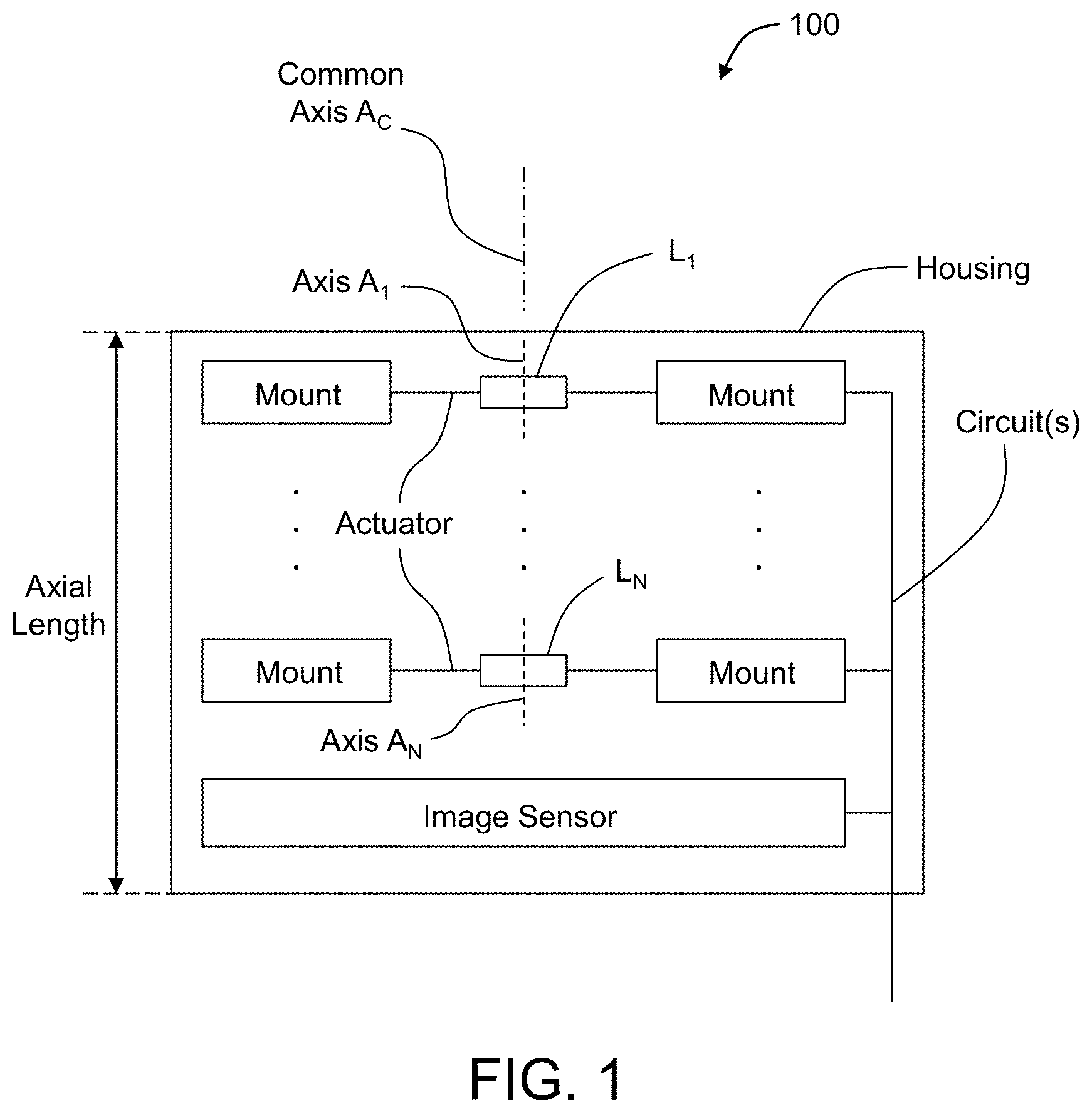
| International Class: | G02B 13/00 20060101 G02B013/00; G02B 7/09 20060101 G02B007/09; G02B 7/10 20060101 G02B007/10; G02B 15/14 20060101 G02B015/14; G02B 15/20 20060101 G02B015/20; G02B 9/64 20060101 G02B009/64; H04N 5/225 20060101 H04N005/225 |
Claims
1. A zoom lens assembly, comprising: a plurality of lens elements, each having an optical axis aligned to a common optical axis, wherein at least one of the plurality of lens elements comprises a movable lens element, at least one of the plurality of lens elements comprises an aspheric lens element, and each of the plurality of lens elements has a lens diameter of 4 millimeters or less; a plurality of lens mounts coupled to the plurality of lens elements, the plurality of lens mounts configured to retain the plurality of lens elements in order; and an actuator coupled between the movable lens element and one of the plurality of lens mounts, the actuator configured to selectively adjust an axial position of the movable lens element along the common optical axis, wherein: an optical zoom of the zoom lens assembly is at least 3.times.; and a maximum axial length of the zoom lens assembly is less than 25 millimeters.
2. The zoom lens assembly of claim 1, wherein a distortion of the zoom lens assembly is less than or equal to 5%.
3. The zoom lens assembly of claim 1, wherein a maximum increase of RMS spot size of the zoom lens assembly is less than or equal to 2X
4. The zoom lens assembly of claim 1, wherein a relative illumination of the zoom lens assembly is greater than 85%.
5. The zoom lens assembly of claim 1, wherein the movable lens element is movable to adjust an effective focal length of the plurality of lens elements between a first effective focal length of about 2.5 millimeters and a second effective focal length of about 10 millimeters.
6. The zoom lens assembly of claim 1, wherein the plurality of lens elements comprises three lens elements.
7. The zoom lens assembly of claim 6, wherein a middle lens element of the three lens elements comprises the movable lens element.
8. The zoom lens assembly of claim 6, wherein: a middle lens element of the three lens elements comprises an input surface and an output surface; the input surface of the middle lens element comprises a first central portion with a convex curvature and a first ring portion surrounding the first central portion, the first ring portion having a concave curvature; and the output surface of the middle lens element comprises a second central portion with a concave curvature and a second ring portion surrounding the second central portion, the second ring portion having a convex curvature.
9. The zoom lens assembly of claim 1, wherein the plurality of lens elements comprises four lens elements.
10. The zoom lens assembly of claim 9, wherein: a first intermediate lens element of the four lens elements comprises a biconcave lens element; and a second intermediate lens element of the four lens elements has an input surface that is convex and an output surface that is concave.
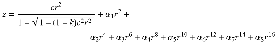
11. The zoom lens assembly of claim 1, wherein surface sag z as a function of radius r of each input surface and output surface of the plurality of lens elements is defined according to: z = cr 2 1 + 1 - ( 1 + k ) c 2 r 2 + .alpha. 1 r 2 + .alpha. 2 r 4 + .alpha. 3 r 6 + .alpha. 4 r 8 + .alpha. 5 r 10 + .alpha. 6 r 12 + .alpha. 7 r 14 + .alpha. 8 r 16 ##EQU00003## wherein: c is curvature, k is the conic constant, and .alpha..sub.1, .alpha..sub.2, .alpha..sub.3, .alpha..sub.4, .alpha..sub.5, .alpha..sub.6, .alpha..sub.7, and .alpha..sub.8 are even aspheric coefficients.
12. A zoom lens assembly, comprising: a housing; an image detector positioned within the housing; a plurality of lens elements positioned within the housing, axially aligned to a common optical axis, and arranged to direct an image onto the image detector, the plurality of lens elements comprising a movable lens element and an aspheric lens element, and each of the plurality of lens elements having a lens volume of 0.003963 cubic centimeters or less; a plurality of lens mounts positioned within the housing and coupled to the plurality of lens elements, the plurality of lens mounts configured to maintain the plurality of lens elements in order within the housing; and an actuator coupled to the movable lens element and configured to selectively move the movable lens element along the common optical axis, wherein: a maximum effective focal length of the plurality of lens elements is at least three times greater than a minimum effective focal length of the plurality of lens elements; and a maximum axial length of the housing is less than 25 millimeters.
13. The zoom lens assembly of claim 12, wherein a distortion of the zoom lens assembly is less than or equal to 5%.
14. The zoom lens assembly of claim 12, wherein a maximum increase of RMS spot size of the zoom lens assembly is less than or equal to 2X.
15. The zoom lens assembly of claim 12, wherein a relative illumination of the zoom lens assembly is greater than 85%.
16. The zoom lens assembly of claim 12, wherein the at least one of the plurality of lens elements comprising the movable lens element is movable to adjust the effective focal length of the plurality of lens elements between a first effective focal length of about 2.5 millimeters and a second effective focal length of about 10 millimeters.
17. The zoom lens assembly of claim 12, wherein: the plurality of lens elements comprises three lens elements; a middle lens element of the three lens elements comprises the movable lens element; the middle lens element comprises an input surface and an output surface; the input surface of the middle lens element comprises a first central portion with a convex curvature and a first ring portion surrounding the first central portion, the first ring portion having a concave curvature; and the output surface of the middle lens element comprises a second central portion with a concave curvature and a second ring portion surrounding the second central portion, the second ring portion having a convex curvature.
18. The zoom lens assembly of claim 12, wherein the plurality of lens elements comprises four lens elements.
19. The zoom lens assembly of claim 18, wherein: a first intermediate lens element of the four lens elements comprises a biconcave lens element; and a second intermediate lens element of the four lens elements has an input surface that is convex and an output surface that is concave.
20. The zoom lens assembly of claim 12, wherein surface sag z as a function of radius r of each input surface and output surface of the plurality of lens elements is defined according to: z = cr 2 1 + 1 - ( 1 + k ) c 2 r 2 + .alpha. 1 r 2 + .alpha. 2 r 4 + .alpha. 3 r 6 + .alpha. 4 r 8 + .alpha. 5 r 10 + .alpha. 6 r 12 + .alpha. 7 r 14 + .alpha. 8 r 16 ##EQU00004## wherein: c is curvature, k is the conic constant, and .alpha..sub.1, .alpha..sub.2, .alpha..sub.3, .alpha..sub.4, .alpha..sub.5, .alpha..sub.6, .alpha..sub.7, and .alpha..sub.8 are even aspheric coefficients.
Description
CROSS-REFERENCE TO RELATED APPLICATION
[0001] This patent application claims the benefit of and priority to U.S. Provisional App. No. 62/808,179 filed Feb. 20, 2019 titled "ZOOM LENS ASSEMBLY," which is incorporated herein by reference.
FIELD OF THE DISCLOSURE
[0002] The present disclosure generally relates to a zoom lens assembly.
BACKGROUND
[0003] Unless otherwise indicated herein, the materials described herein are not prior art to the claims in the present application and are not admitted to be prior art by inclusion in this section.
[0004] Digital imagers (e.g., cameras) are increasingly being incorporated into consumer devices, such as cellular telephones (e.g., "smartphones"), tablet devices, and the like. As their use increases, there is a related demand for the imagers to deliver a wider range of performance abilities. For example, consumers expect a smartphone camera to be able to change the angle of view (i.e., "zoom," "telephoto," or "wide-angle" focus) and to auto-focus. However, given the relatively small form factor for many of these consumer devices, it is difficult to incorporate the movable lens systems that would enable higher quality optical abilities. Typically, smartphone cameras, and the like, use software routines to mimic zoom or wide-angle focus abilities, but they usually deliver lesser quality images.
[0005] The subject matter claimed herein is not limited to embodiments that solve any disadvantages or that operate only in environments such as those described above. Rather, this background is only provided to illustrate one example technology area where some embodiments described herein may be practiced.
SUMMARY
[0006] An example zoom lens assembly may include lens elements, lens mounts, and an actuator. Each of the lens elements has an optical axis aligned to a common optical axis. At least one of the lens elements is a movable lens element and at least one of the lens elements is an aspheric lens element. Each of the lens elements has a lens diameter of 4 millimeters or less. The lens mounts are coupled to the lens elements and are configured to retain the lens elements in order. The actuator is coupled between the movable lens element and one of the lens mounts. The actuator is configured to selectively adjust an axial position of the movable lens element along the common optical axis. An optical zoom of the zoom lens assembly is at least 3.times.. A maximum axial length of the zoom lens assembly is less than 25 millimeters.
[0007] Another example zoom lens assembly may include a housing, an image detector, lens elements, lens mounts, and an actuator. The image detector is positioned within the housing. The lens elements are positioned within the housing, are axially aligned to a common optical axis, and are arranged to direct an image onto the image detector. The lens elements include a movable lens element and an aspheric lens element. Each of the lens elements has a lens volume of 0.003963 cubic centimeters or less. The lens mounts are positioned within the housing and are coupled to the lens elements. The lens mounts are configured to maintain the lens elements in order within the housing. The actuator is coupled to the movable lens element and is configured to selectively move the movable lens element along the common optical axis. A maximum effective focal length of the lens elements is at least three times greater than a minimum effective focal length of the lens elements. A maximum axial length of the housing is less than 25 millimeters.
BRIEF DESCRIPTION OF THE DRAWINGS
[0008] Example implementations will be described and explained with additional specificity and detail through the use of the accompanying drawings in which:
[0009] FIG. 1 illustrates an example zoom lens assembly;
[0010] FIGS. 2A-2C illustrate an example first set of lens elements L.sub.1, L.sub.2, and L.sub.3 that may be included in the zoom lens assembly of FIG. 1;
[0011] FIG. 3 is a side view of the lens elements of FIGS. 2A-2C at different configurations or zoom ratios;
[0012] FIG. 4 includes two tables summarizing properties of the three lens elements of FIGS. 2A-3 in combination;
[0013] FIGS. 5A-5C include simulated spot diagrams for the three lens elements of FIGS. 2A-2C in each of the three configurations of FIG. 3;
[0014] FIGS. 6A-6C include simulated modulation transfer functions for the three lens elements of FIGS. 2A-2C in each of the three configurations of FIG. 3;
[0015] FIG. 7 includes simulated distortion for the three lens elements of FIGS. 2A-2C in each of the three configurations of FIG. 3 and for each of three wavelengths;
[0016] FIG. 8 includes simulated chromatic focal shift verses wavelength for the three lens elements of FIGS. 2A-2C in each of the three configurations of FIG. 3;
[0017] FIG. 9 includes simulated relative illumination as a function of Y field for the three lens elements of FIGS. 2A-2C in each of the three configurations of FIG. 3;
[0018] FIGS. 10A and 10B illustrate an example second set of lens elements L.sub.1, L.sub.2, L.sub.3, and L.sub.4 that may be included in the zoom lens assembly of FIG. 1; and
[0019] FIG. 11 illustrates a block diagram of an example computing device, all arranged in accordance with at least one embodiment described herein.
DETAILED DESCRIPTION
[0020] The detailed description set forth below includes a description of various configurations of the subject technology and is not intended to represent the only configurations in which the subject technology may be practiced. The detailed description includes specific details for the purpose of providing a thorough understanding of the subject technology. However, the subject technology may be practiced without these specific details. In some instances, well-known structures and components are not shown, or are shown schematically, to avoid obscuring the concepts of the subject technology.
[0021] Some zoom lens assemblies use spherical lenses. Spherical lenses usually introduce aberrations in imaging (e.g., spherical aberration) which needs one or more lenses to correct. Furthermore, zoom lens systems typically need additional optical components to compensate for image quality degradation during zooming. Due to such compounded complexity, although zoom lens assemblies with spherical lenses have been miniaturized to the extent possible, they typically cannot be miniaturized sufficiently to fit within many small form factors, e.g., form factors having a maximum axial length of 25 millimeters (mm) or less, without creating significant image degradation due to the physics of light in spherical lenses.
[0022] Some embodiments disclosed herein relate to a small form factor zoom lens assembly that may have an axial length (e.g., along an optical axis of the zoom lens assembly) of 25 mm or less. For example, the zoom lens assembly may include multiple lens elements and an image sensor packaged within a housing, and the housing may have an axial length of 25 mm or less. At least one of the lens elements may include an aspheric lens element. In some embodiments, at least one of the lens elements may include a spherical lens element. In other embodiments, all of the lens elements may include aspheric lens elements. The lens elements may be axially aligned.
[0023] The zoom lens assembly may have an optical zoom of at least 3.times.. In particular, a maximum effective focal length of the zoom lens assembly may be at least three times greater than a minimum effective focal length of the zoom lens assembly. Optionally, the optical zoom of the zoom lens assembly may be at least 4.times., 10.times., or even higher.
[0024] Notwithstanding the small form factor of the zoom lens assembly according to some embodiments, it may have a distortion of 5% or less, a maximum .about.2.times. increase of RMS spot size or less, and a relative illumination of 85% or more.
[0025] In some embodiments, the lens elements of the zoom lens assembly may include at least one movable lens element(s) that is movable to adjust an effective focal length of the lens elements between at least a first effective focal length and a second effective focal length. For example, the first and second effective focal lengths may be, respectively, 2.5 mm and 10 mm. The movable lens element(s) may be movable in some embodiments to adjust the effective focal length of the lens elements between more than two effective focal lengths, such as between three or even more focal lengths. For example, the movable lens element(s) may be movable to adjust the effective focal length of the lens elements between effective focal lengths of 2.5 mm, 5 mm, and 10 mm.
[0026] In some embodiments, the lens elements include three axially aligned lens elements where at least the middle lens element is movable. Each lens element may have two surfaces, including an input surface and an output surface. In general, incoming light may enter a lens element through the input surface and may exit the lens element through the output surface. Thus, the output surface of each lens element may face the image sensor of the zoom lens assembly.
[0027] In some embodiments, the middle lens element has complex aspherical input and output surfaces. For example, the input surface of the middle lens element may include a first central portion with a convex curvature and a first ring portion surrounding the first central portion, the first ring portion having a concave curvature. The output surface of the middle lens element may include a second central portion with a concave curvature and a second ring portion surrounding the second central portion, the second ring portion having a convex curvature.
[0028] In some embodiments, the lens elements include four axially aligned lens elements. Thus, the four lens elements may include two intermediate lens elements positioned between two end lens elements. One of the intermediate lens elements may include a biconcave lens element. The other of the intermediate lens elements may have an input surface that is convex and an output surface that is concave.
[0029] FIG. 1 illustrates an example zoom lens assembly 100, arranged in accordance with at least one embodiment described herein. The zoom lens assembly 100 may include two or more lens elements, labeled in FIG. 1 as lens element Li and lens element L.sub.N, where "N" is an integer of 2 or higher. Each of the lens elements has an optical axis, labeled in FIG. 1 as Axis A.sub.1 and Axis A.sub.N. The optical axes of the lens elements may be aligned to a common optical axis, labeled Common Axis A.sub.C in FIG. 1. Accordingly, all of the lens elements of the zoom lens assembly 100 may be optically aligned with each other.
[0030] At least one of the lens elements may be a movable lens element, e.g., movable along the common optical axis. At least one of the lens elements may be an aspheric lens element. The movable lens element and the aspheric lens element may be the same lens element or different lens elements. In some embodiments, two or more lens elements may be movable lens elements and/or two or more lens elements may be aspheric lens elements. In some embodiments, all of the lens elements may be both movable lens elements and aspheric lens elements.
[0031] The zoom lens assembly 100 may also include two or more lens mounts, each of which is labeled "Mount" in FIG. 1. The lens mounts may be coupled directly or indirectly to the lens elements. The lens mounts may be configured to support and retain the lens elements in order, e.g., within a housing. Each of the lens mounts may include a substrate or strata to or on which a corresponding one of the lens elements may be coupled and/or formed, or other suitable structure to support and retain the lens elements.
[0032] The housing may include glass, plastic, metal, or other suitable materials to enclose therein the other elements of the zoom lens assembly 100. In some embodiments, the housing hermetically seals therein the other elements of the zoom lens assembly 100.
[0033] As already mentioned, at least one of the lens elements may be a movable lens element. Accordingly, the zoom lens assembly 100 may further include an actuator coupled to the movable lens element. Where multiple lens elements are movable lens elements, the zoom lens assembly 100 may include multiple actuators. For example, two actuators are illustrated in FIG. 1, one actuator for each of the lens elements. In some embodiments, multiple actuators may be coupled to a single lens element to adjust the single lens element. Alternatively or additionally, a single actuator may be coupled to multiple lens elements to adjust multiple lens elements.
[0034] The lens mounts and actuators of the zoom lens assembly 100 may include any suitable lens mounts and/or actuators assembled using any suitable process and/or may be implemented as a micro-opto-electro-mechanical system (MOEMS). Some examples that may be suitable for small form factors are disclosed in U.S. Publication No. 2017/0205603 (hereinafter the '603 publication), which is incorporated herein by reference in its entirety. According to the '603 publication, for instance, various wafers may be formed with various lens holders and lens actuator systems (e.g., analogous to the lens mounts and/or actuators described herein) and then a lens element may be coupled to and/or formed on each of the lens holders and lens actuator systems. The wafers may then be stacked together, coupled, and diced into multiple stacked zoom lens systems (e.g., analogous to the zoom lens assemblies described herein). Embodiments described herein may be implemented using the same, similar, or different techniques and/or the same, similar, or different materials from those described in the '603 publication.
[0035] The zoom lens assembly 100 may additionally include an image sensor and one or more electrical circuits. The image sensor may include a charge-coupled device (CCD), an active-pixel sensor (APS) such as a complementary metal-oxide-semiconductor (CMOS) sensor, or other suitable image sensor. The electrical circuits may communicate electrical signals between one or more of the image sensor or the actuators and one or more other devices that may be internal or external to the housing. For example, the electrical circuits may communicate control signals to one or both of the actuators which may cause the corresponding actuator(s) to adjust a position of the corresponding lens element(s) along the common optical axis, e.g., to adjust an effective focal length and thus angle of view of the zoom lens assembly 100.
[0036] The one or more other devices to which the image sensor and/or actuators are electrically coupled via the electrical circuits may include, e.g., a driver, a processor, a microprocessor, a controller, a microcontroller, an application specific integrated circuit (ASIC), a field programmable gate array (FPGA), or other device. Alternatively or additionally, the one or more other devices to which the image sensor and/or actuators are electrical coupled via the electrical circuits may include, e.g., a gyroscope, accelerometer, magnetometer, or other device(s) for image stabilization or other purpose(s).
[0037] The zoom lens assembly 100 may have a small form factor. For example, the zoom lens assembly 100 may have a maximum effective focal length of 25 mm or less, and/or the housing may have an axial length of 25 mm or less. Alternatively or additionally, the maximum effective focal length of the zoom lens assembly 100 and/or the axial length of the housing may be 15 mm or less or 10 mm or less.
[0038] The zoom lens assembly 100 may have an optical zoom of at least 3.times.. In particular, a maximum effective focal length of the zoom lens assembly may be at least three times greater than a minimum effective focal length of the zoom lens assembly. Optionally, the optical zoom of the zoom lens assembly 100 may be at least 4.times., 10.times., or even higher. For example, the zoom lens assembly 100 may have a minimum effective focal length of 2.5 mm and a maximum effective focal length of 10 mm. Optionally, the zoom lens assembly 100 may further have an intermediate effective focal length of 5 mm.
[0039] Notwithstanding the small form factor of the zoom lens assembly according to some embodiments, it may have a distortion of 5% or less or even 3% or less, a maximum 2X increase of RMS spot size or less, and a relative illumination of 85% or more.
[0040] Various specific combinations of numbers N and shapes of lens elements may be implemented to satisfy a particular zoom lens assembly target (hereinafter "target"). The target as used herein may include at least a minimum zoom threshold (e.g., a minimum zoom of 3.times.) and a maximum axial length threshold (e.g., a maximum axial length of 25 mm or less). In some embodiments, the target may further include one or more of a maximum distortion threshold (e.g., a distortion of 5% or less), a maximum RMS spot size increase threshold (e.g., a .about.2X increase of RMS spot size), and/or a minimum relative illumination threshold (e.g., a relative illumination of 85% or more). Two specific combinations of numbers N and shapes of lens elements will be described that satisfy the target as described herein. Other specific combinations of numbers N and shapes of lens elements may alternatively be implemented to satisfy the target.
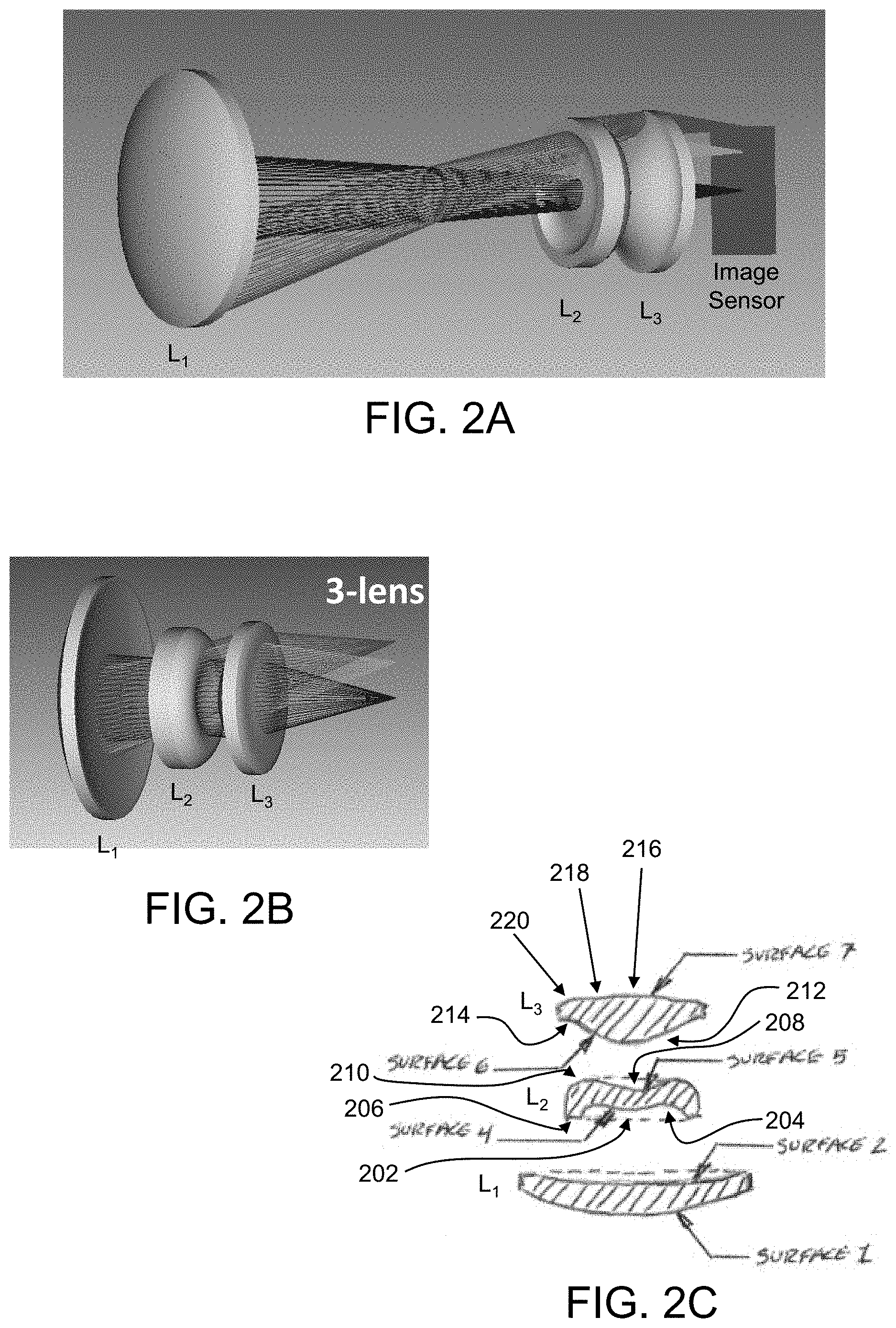
[0041] FIGS. 2A-2C illustrate an example first set of lens elements L.sub.1, L.sub.2,l and L.sub.3 that may be included in the zoom lens assembly of FIG. 1, arranged in accordance with at least one embodiment described herein. In particular, FIG. 2A illustrates a front and right side perspective view of the first set of lens elements, FIG. 2B illustrates a rear and right side perspective view of the first set of lens elements, and FIG. 2C illustrates a cross-sectional side view of the first set of lens elements. The first set of lens elements have a different relative spacing in FIG. 2A than in FIGS. 2B and 2C, which may be achieved by moving one or more of the lens elements axially relative to the other lens elements and/or relative to the image sensor (FIG. 2A). For example, at least the middle or second lens element L.sub.2 may be movable.
[0042] As illustrated in FIGS. 2A-2C, each of the lens elements is an aspheric lens element.
[0043] The input surface of the first lens element L.sub.1, labeled "SURFACE 1" in FIG. 2C, may be convex. The output surface of the first lens element L.sub.1, labeled "SURFACE 2" in FIG. 2C, may be concave, or substantially concave. Thus, the first lens element L.sub.1 may be or may substantially be a meniscus lens element, and in particular a positive meniscus lens element.
[0044] The input surface of the second lens element L.sub.2, labeled "SURFACE 4" in FIG. 2C, may have a more complex curvature than simply concave, convex, or planar. For example, as illustrated, the input surface of the second lens element L.sub.2 includes a first central portion 202 (FIG. 2C) with a convex curvature, surrounded by a first ring portion 204 (FIG. 2C) with a concave curvature, which is in turn surrounded by a planar ring portion 206 (FIG. 2C). The output surface of the second lens element L.sub.2, labeled "SURFACE 5" in FIG. 2C, includes a second central portion 208 (FIG. 2C) with a concave curvature, surrounded by a second ring portion 210 (FIG. 2C) with a convex curvature.
[0045] Thus, the curvature of the output surface of the second lens element L.sub.2 generally follows the curvature of the input surface of the second lens element L.sub.2. In particular, where the first central portion 202 of the input surface protrudes towards the first lens element L.sub.1, the second central portion 208 of the output surface similarly protrudes towards the first lens element L.sub.1. Analogously, where the first ring portion 204 of the input surface protrudes away from the first lens element L.sub.1, the second ring portion 210 of the output surface similarly protrudes away from the first lens element L.sub.1.
[0046] The input surface of the third lens element L.sub.3, labeled "SURFACE 6" in FIG. 2C, includes a first central portion 212 (FIG. 2C) with a convex curvature surrounded by a first ring portion 214 (FIG. 2C) with a concave and/or planar curvature. The output surface of the third lens element L.sub.3, labeled "SURFACE 7" in FIG. 2C, includes a second central portion 216 (FIG. 2C) with a convex curvature, surrounded by a second ring portion 218 (FIG. 2C) with a concave curvature, which in turn is surrounded by a third ring portion 220 (FIG. 2C) with a convex curvature.
[0047] In some embodiments, the surface sag of the lens elements of FIGS. 2A-2C may be described by an nth order polynomial. In an example, the surface sag z(r) of the lens elements of FIGS. 2A-2C may be described particularly by a 16th order polynomial as equation 1:
z = cr 2 1 + 1 - ( 1 + k ) c 2 r 2 + .alpha. 1 r 2 + .alpha. 2 r 4 + .alpha. 3 r 6 + .alpha. 4 r 8 + .alpha. 5 r 10 + .alpha. 6 r 12 + .alpha. 7 r 14 + .alpha. 8 r 16 ##EQU00001##
In equation 1, c is curvature (i.e., 1/radius), k is the conic constant, and .alpha..sub.1, .alpha..sub.2, .alpha..sub.3, .alpha..sub.4, .alpha..sub.5, .alpha..sub.6, .alpha..sub.7, and .alpha..sub.8 are even aspheric coefficients. Optical polymer E48R may be used as lens material for each of the lens elements of FIGS. 2A-2C. More generally, each of the lens elements of FIGS. 2A-2C may include cyclic olefin polymer (COP) such as E48R or other suitable lens material.
[0048] Tables 1.1, 1.2, and 1.3 below (hereinafter collectively "Table 1") define the size, surface shape (in connection with equation 1--see above), and other parameters of the lens elements of FIGS. 2A-2C, arranged in accordance with at least one embodiment described herein. In the surface data summary (Table 1.1), optical media are cascaded one after another: if the Glass type of a surface is E48R, it means this surface is followed by the medium E48R (i.e., front surface of a lens); if the Glass type is Air, it means this surface is followed by air (i.e., back surface of a lens or an air gap). In addition, aspherical surfaces are designated as EVENASPH. For each design, also listed (in Table 1.3) are the variable air-gap thicknesses between lenses at different configurations (i.e., zoom ratios). In Table 1.3, "Thickness 2" refers to the variable air-gap thickness between the first lens element Li and the lens stop ("STO" in Table 1) of the lens elements, "Thickness 3" refers to the variable air-gap thickness between the lens stop and the second lens element L.sub.2, "Thickness 5" refers to the variable air-gap thickness between the second and third lens elements L.sub.2 and L.sub.3, and "Thickness 7" refers to the variable air-gap thickness between the third lens element L.sub.3 and the image sensor. The lens parameters and thicknesses may be fixed across different configurations.
[0049] In more detail, Table 1.1 below includes a summary of various aspects of the lens elements of FIGS. 2A in accordance with at least one embodiment described herein. In Table 1, OBJ refers to object, STO refers to lens stop (or the overall aperture of the system--see "STO" label in FIG. 3), and IMA refers to image plane.
TABLE-US-00001 TABLE 1.1 SURFACE DATA SUMMARY: Surf Type Radius Thickness Glass Diameter OBJ STANDARD Infinity Infinity 0 1 EVENASPH 4.397642 0.4979031 E48R 3.359122 2 EVENASPH 29.04766 0.7183437 air 3.241345 STO STANDARD Infinity 0.3374206 air 1.109969 4 EVENASPH 1.460748 0.2883756 E48R 1.617162 5 EVENASPH 1.18486 0.3335344 air 1.955452 6 EVENASPH 1.234586 0.700246 E48R 2.08643 7 EVENASPH -3.189324 1.842095 air 2.117686 IMA STANDARD Infinity 1.568774
[0050] Table 1.2 below includes details of the lens elements of FIGS. 2A-2C defined according to equation 1 in accordance with at least one embodiment described herein. In Table 1.2, "Coefficient on r.LAMBDA.2" for a given surface refers to the aspheric coefficient .alpha..sub.1 in equation 1 for the surface, "Coefficient on r.LAMBDA.4" for a given surface refers to the aspheric coefficient .alpha..sub.2 in equation 1 for the surface, "Coefficient on r.LAMBDA.6" for a given surface refers to the aspheric coefficient .alpha..sub.3 in equation 1 for the surface, and so on.
TABLE-US-00002 TABLE 1.2 SURFACE DATA DETAIL: Surface 1 EVENASPH Coefficient on r{circumflex over ( )} 2: 0.0017816445 Coefficient on r{circumflex over ( )} 4: -0.0028713675 Coefficient on r{circumflex over ( )} 6: 0.0083098647 Coefficient on r{circumflex over ( )} 8: -0.001851218 Coefficient on r{circumflex over ( )} 10: 0.00028992335 Coefficient on r{circumflex over ( )} 12: -5.8167723e-005 Coefficient on r{circumflex over ( )} 14: 0 Coefficient on r{circumflex over ( )} 16: 0 Surface 2 EVENASPH Coefficient on r{circumflex over ( )} 2: -0.0016105071 Coefficient on r{circumflex over ( )} 4: 0.0014407448 Coefficient on r{circumflex over ( )} 6: 0.0056689841 Coefficient on r{circumflex over ( )} 8: 0.00072096442 Coefficient on r{circumflex over ( )} 10: -0.00098297017 Coefficient on r{circumflex over ( )} 12: 0.00013497457 Coefficient on r{circumflex over ( )} 14: 0 Coefficient on r{circumflex over ( )} 16: 0 Surface STO STANDARD Surface 4 EVENASPH Coefficient on r{circumflex over ( )} 2: -0.018846734 Coefficient on r{circumflex over ( )} 4: -0.79186679 Coefficient on r{circumflex over ( )} 6: 0.24222451 Coefficient on r{circumflex over ( )} 8: -0.078696143 Coefficient on r{circumflex over ( )} 10: -0.44775963 Coefficient on r{circumflex over ( )} 12: -0.054637139 Coefficient on r{circumflex over ( )} 14: 0 Coefficient on r{circumflex over ( )} 16: 0 Surface 5 EVENASPH Coefficient on r{circumflex over ( )} 2: 0.29878818 Coefficient on r{circumflex over ( )} 4: -1.0731624 Coefficient on r{circumflex over ( )} 6: 0.14536946 Coefficient on r{circumflex over ( )} 8: 0.078992381 Coefficient on r{circumflex over ( )} 10: -0.030373589 Coefficient on r{circumflex over ( )} 12: -0.1022783 Coefficient on r{circumflex over ( )} 14: 0 Coefficient on r{circumflex over ( )} 16: 0 Surface 6 EVENASPH Coefficient on r{circumflex over ( )} 2: 0.042165142 Coefficient on r{circumflex over ( )} 4: 0.051940991 Coefficient on r{circumflex over ( )} 6: -0.33077437 Coefficient on r{circumflex over ( )} 8: 0.38617929 Coefficient on r{circumflex over ( )} 10: -0.39816509 Coefficient on r{circumflex over ( )} 12: 0.11228655 Coefficient on r{circumflex over ( )} 14: 0 Coefficient on r{circumflex over ( )} 16: 0 Surface 7 EVENASPH Coefficient on r{circumflex over ( )} 2: -0.091215149 Coefficient on r{circumflex over ( )} 4: 0.18235242 Coefficient on r{circumflex over ( )} 6: 0.23602258 Coefficient on r{circumflex over ( )} 8: -0.21601076 Coefficient on r{circumflex over ( )} 10: -0.16245715 Coefficient on r{circumflex over ( )} 12: 0.11378482 Coefficient on r{circumflex over ( )} 14: 0 Coefficient on r{circumflex over ( )} 16: 0
[0051] Table 1.3 below includes details of the edge thickness in mm of the surfaces of the lens elements of FIGS. 2A-2C in accordance with at least one embodiment described herein. Table 1.3 also lists the variable air-gap thicknesses between lenses at different configurations (i.e., zoom ratios). The edge thickness is defined herein as the separation of two surfaces at their edge, defined as Z.sub.i-1-Z.sub.i+T.sub.i, where Z.sub.i is the sag of the surface i, Z.sub.i+i is the sag of the next surface, and T.sub.i is the axial thickness of the surface i. For STO, the edge thickness is referenced to the next surface. For IMG, there is no next surface to reference, so its edge thickness is 0.
TABLE-US-00003 EDGE THICKNESS DATA: Surf Edge 1 0.200000 2 0.608912 STO 0.226369 4 0.310589 5 0.798203 6 0.199989 7 1.966521 IMA 0.000000 MULTI-CONFIGURATION DATA: Configuration 1: 1 Thickness 2: 0.7183437 Variable 2 Thickness 3: 0.3374206 Variable 3 Thickness 5: 0.3335344 Variable 4 Thickness 7: 1.842095 Variable Configuration 2: 1 Thickness 2: 3.648315 Variable 2 Thickness 3: 2.161279 Variable 3 Thickness 5: 0.3544034 Variable 4 Thickness 7: 1.201386 Variable Configuration 3: 1 Thickness 2: 2.727257 Variable 2 Thickness 3: 5.227129 Variable 3 Thickness 5: 0.5091548 Variable 4 Thickness 7: 0.04995443 Variable
[0052] FIG. 3 is a side view of the lens elements of FIGS. 2A-2C at different configurations or zoom ratios, arranged in accordance with at least one embodiment described herein. The configurations of FIG. 3 may correspond to and/or include configurations 1, 2, and 3 of Table 1. For example, Configuration 1 of FIG. 3 may correspond to and/or include Configuration 1 of Table 1, Configuration 2 of FIG. 3 may correspond to and/or include Configuration 2 of Table 1, and Configuration 3 of FIG. 3 may correspond to and/or include Configuration 3 of Table 1.
[0053] According to Configuration 1, the first lens element Li may be positioned approximately 1 mm from the second lens element L.sub.2 (or specifically 1.0557643 mm according to Table 1), the second lens element L.sub.2 may be positioned approximately 0.3 mm from the third lens element L.sub.3 (or specifically 0.3335344 mm according to Table 1), and the third lens element L.sub.3 may be positioned approximately 1.8 mm from the image sensor (or specifically 1.842095 mm according to Table 1) to achieve an effective focal length of 2.5 mm for the three lens elements in combination.
[0054] According to Configuration 2, the first lens element Li may be positioned approximately 6 mm from the second lens element L.sub.2 (or specifically 5.809594 mm according to Table 1), the second lens element L.sub.2 may be positioned approximately 0.3 mm from the third lens element L.sub.3 (or specifically 0.3544034 mm according to Table 1), and the third lens element L.sub.3 may be positioned approximately 1.1 mm from the image sensor (or specifically 1.201386 mm according to Table 1) to achieve an effective focal length of 5 mm for the three lens elements in combination.
[0055] According to Configuration 3, the first lens element Li may be positioned approximately 8 mm from the second lens element L.sub.2 (or specifically 7.954386 mm according to Table 1), the second lens element L.sub.2 may be positioned approximately 0.5 mm from the third lens element L.sub.3 (or specifically 0.0.5091548 mm according to Table 1), and the third lens element L.sub.3 may be positioned approximately 0.1 mm from the image sensor (or specifically 0.04995443 mm according to Table 1) to achieve an effective focal length of 10 mm for the three lens elements in combination.
[0056] FIG. 4 includes two tables summarizing properties of the three lens elements of FIGS. 2A-3 in combination, arranged in accordance with at least one embodiment described herein. According to the upper table of FIG. 4, the three lens elements of FIGS. 2A-3 may be suitable for light having wavelengths in the range from about 486 nanometers to about 656 nanometers, lens diameters of the lens elements may be in a range from about 2 mm to about 3.2 mm, the three lens elements in combination may have optical zoom of 4.times. and three different effective focal lengths of 2.5 mm, 5 mm, and 10 mm, the three lens elements in combination may have an aperture (F#) of 2, 4, or 8, the three lens elements in combination may have a field of view of about 40 degrees, the three lens elements in combination may have a distortion of less than 5% such as a distortion in a range from 0.5% to 2.8%, and the three lens elements in combination may have a relative illumination of at least 85%. The lower table of FIG. 4 lists the volume, density, and mass of the three lens elements when implemented with optical polymer E48R according to an example implementation.
[0057] As disclosed in FIG. 4, each lens element in the first set of lens elements of FIGS. 2A-3 has a lens diameter of 3.2 mm or less. More generally, each lens element of this and other embodiments may have a lens diameter of 4 mm or less. In addition, each lens element in the first set of lens elements of FIGS. 2A-3 has a lens volume of 0.003170 cubic centimeters (cc). More generally, each lens element of this and other embodiments may have a lens volume of 0.003963 cc or less. Further, each lens element in the first set of lens elements of FIGS. 2A-3 has a lens mass of 0.003202 grams (g). More generally, each lens element of this and other embodiments may have a lens mass of 0.004003 g or less.
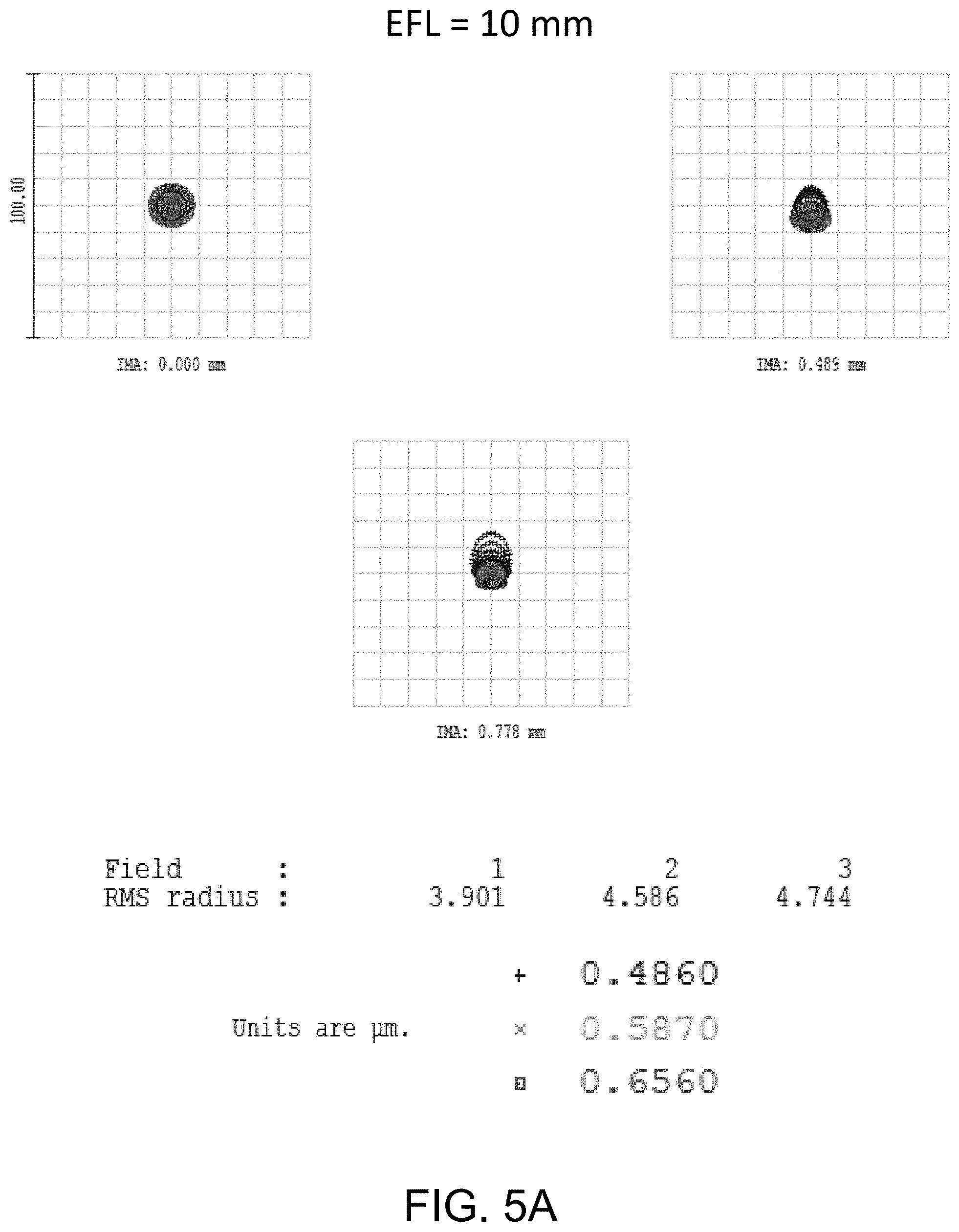
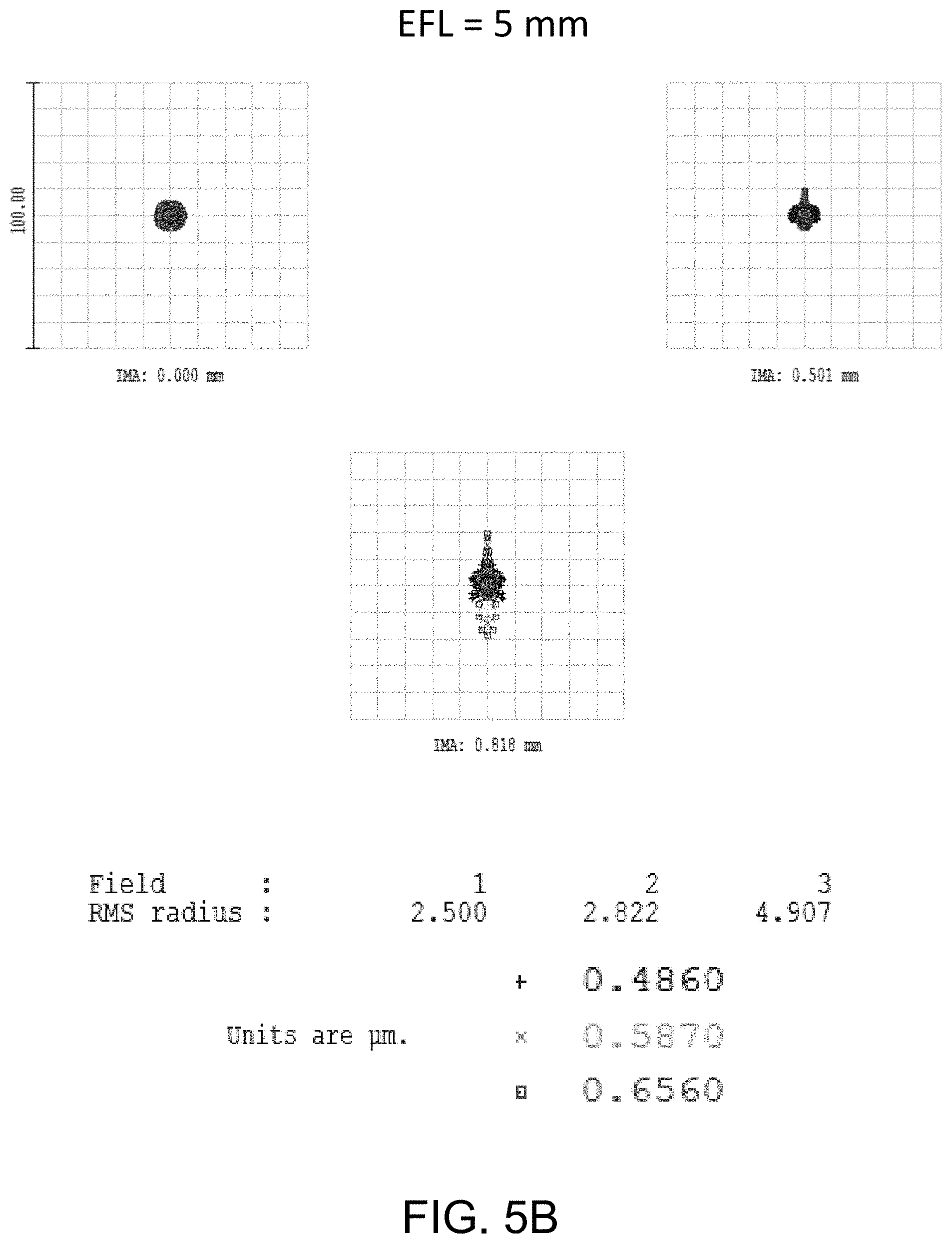
[0058] FIGS. 5A-5C include simulated spot diagrams for the three lens elements of FIGS. 2A-2C in each of the three configurations of FIG. 3, arranged in accordance with at least one embodiment described herein. FIG. 5A includes the simulated spot diagram for Configuration 3 having an effective focal length of 10 mm as indicated by the label "EFL=10 mm" at the top of the Figure. FIG. 5B includes the simulated spot diagram for Configuration 2 having an effective focal length of 5 mm as indicated by the label "EFL=5 mm" at the top of the Figure. FIG. 5C includes the simulated spot diagram for Configuration 1 having an effective focal length of 2.5 mm as indicated by the label "EFL=2.5 mm" at the top of the Figure. It can be seen from FIGS. 5A-5C that the focus spot maintains high quality during the zooming process including specifically at each of the effective focal lengths of, respectively, 10 mm, 5 mm, and 2.5 mm.
[0059] FIGS. 6A-6C include simulated modulation transfer functions (MTFs) for the three lens elements of FIGS. 2A-2C in each of the three configurations of FIG. 3, arranged in accordance with at least one embodiment described herein. The horizontal axis is spatial frequency in cycles per mm incremented at intervals of 15 cycles per mm and beginning at 0. The vertical axis is modulus of the optical transfer function incremented at intervals of 0.1 and beginning at 0.
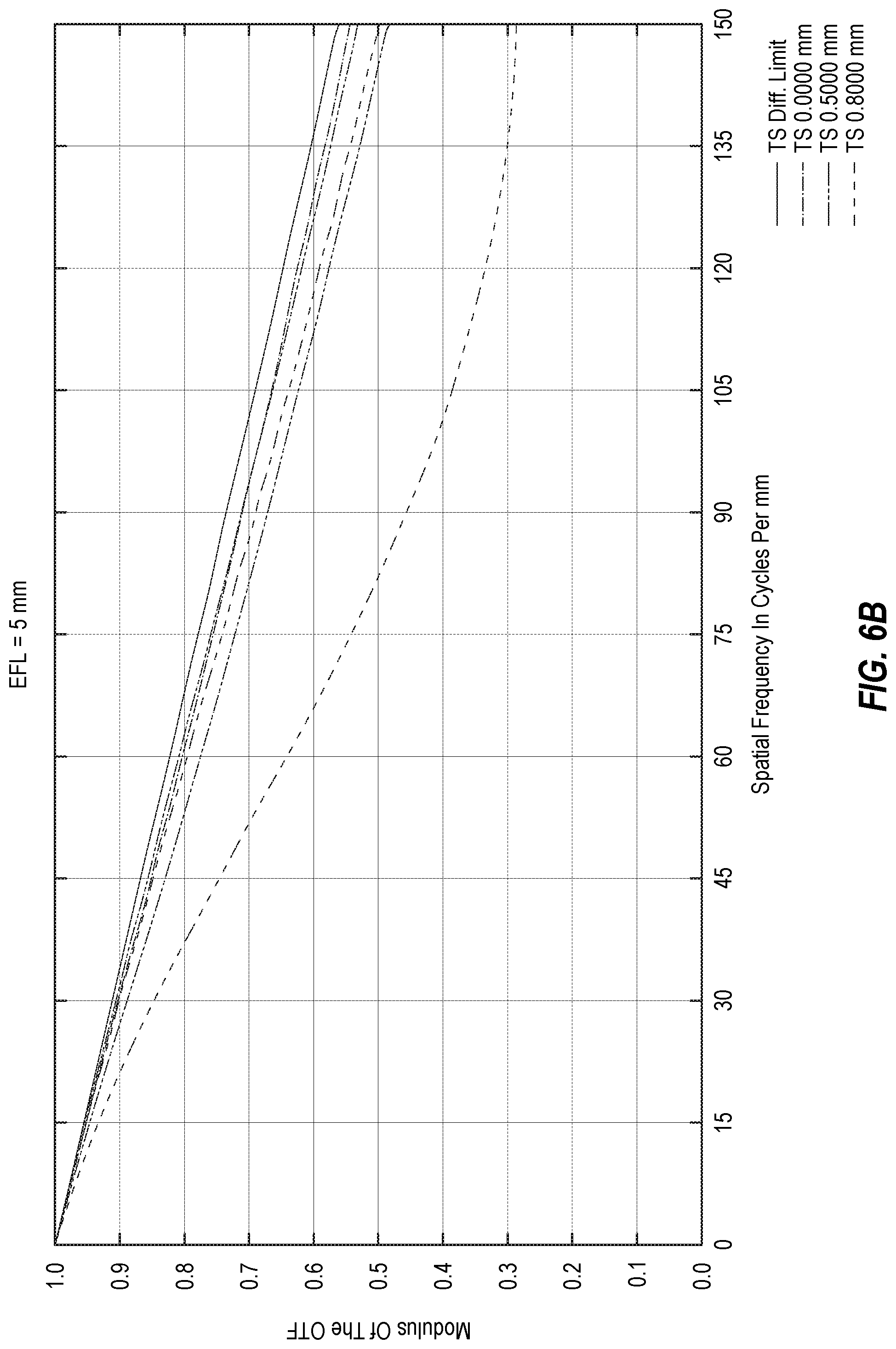
[0060] FIG. 6A includes the simulated MTF for Configuration 3 having an effective focal length of 10 mm as indicated by the label "EFL=10 mm" at the top of the Figure. FIG. 6B includes the simulated MTF for Configuration 2 having an effective focal length of 5 mm as indicated by the label "EFL=5 mm" at the top of the Figure. FIG. 6C includes the simulated MTF for Configuration 1 having an effective focal length of 2.5 mm as indicated by the label "EFL=2.5 mm" at the top of the Figure. In FIGS. 6A-6C, the black curve(s) labeled "TS Diff. Limit" correspond to a diffraction limit situation, e.g., a perfect lens; the blue curve(s) labeled "TS 0.000 mm" correspond to the first lens element L.sub.1, the green curve(s) labeled "TS 0.500 mm" correspond to the second lens element L.sub.2, and the red curve(s) labeled "TS 0.8000 mm" correspond to the third lens element L.sub.3. It can be seen from FIGS. 6A-6C that high quality imaging is maintained across different zoom ratios.
[0061] FIG. 7 includes simulated distortion for the three lens elements of FIGS. 2A-2C in each of the three configurations of FIG. 3 and for each of three wavelengths, arranged in accordance with at least one embodiment described herein. The horizontal axis is percent distortion from 0 (in the middle) to plus or minus 0.5 percent in the top left simulation, and from 0 (in the middle) to plus or minus 5 percent in the middle right and bottom left simulations. The vertical axis in all three simulations is field angle. Thus, the graphs of FIG. 7 show distortion as a function of field angle for each of three different wavelengths.
[0062] The three wavelengths included in each simulation include 0.486 micrometers (e.g., 486 nanometers), 0.587 micrometers (e.g., 587 nanometers), and 0.656 micrometers (e.g., 656 nanometers), as indicated by the labels applied to each curve. The simulated distortion for Configuration 3 having an effective focal length of 10 mm appears directly under the label "EFL=10 mm" in FIG. 7. The simulated distortion for Configuration 2 having an effective focal length of 5 mm appears directly under the label "EFL=5 mm" in FIG. 7. The simulated distortion for Configuration 1 having an effective focal length of 2.5 mm appears directly under the label "EFL=2.5 mm" in FIG. 7. It can be seen from FIG. 7 that the distortion of the optical system is maintained below 5% across different zoom ratios.
[0063] FIG. 8 includes simulated chromatic focal shift verses wavelength for the three lens elements of FIGS. 2A-2C in each of the three configurations of FIG. 3, arranged in accordance with at least one embodiment described herein. The horizontal axis in each of the three simulations of FIG. 8 is focal shift in micrometers. In the top left simulation, the horizontal axis is incremented in intervals of 40 micrometers beginning at -200 micrometers on the left and ending at 200 micrometers on the right. In the middle right simulation and the bottom left simulation, the horizontal axis is incremented in intervals of 10 micrometers beginning at -50 micrometers on the left and ending at 50 micrometers on the right. The vertical axis in each of the three simulations of FIG. 8 is wavelength in micrometers incremented in intervals of 0.017 micrometers beginning at 0.486 micrometers at the bottom and ending at 0.656 micrometers at the top.
[0064] The simulated focal shift for Configuration 3 having an effective focal length of 10 mm appears directly under the label "EFL=10 mm" in FIG. 8. The simulated focal shift for Configuration 2 having an effective focal length of 5 mm appears directly under the label "EFL=5 mm" in FIG. 8. The simulated focal shift for Configuration 1 having an effective focal length of 2.5 mm appears directly under the label "EFL=2.5 mm" in FIG. 8. It can be seen from FIG. 8 that the variance of focal spot size across the spectral range is minimized during the zooming process including specifically at each of the effective focal lengths of, respectively, 10 mm, 5 mm, and 2.5 mm.
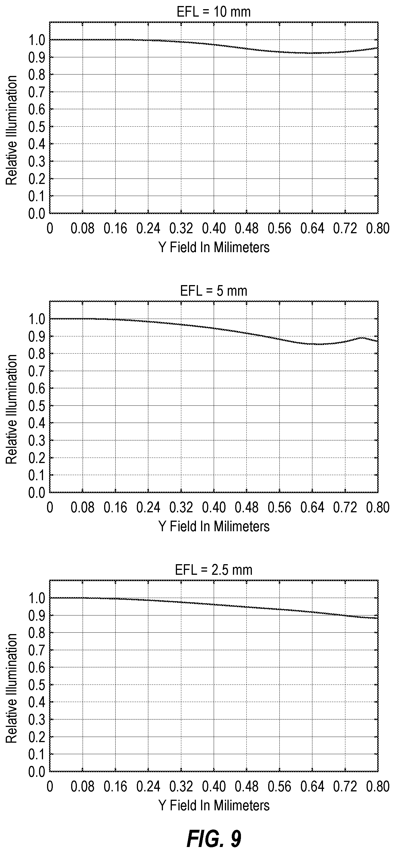
[0065] FIG. 9 includes simulated relative illumination as a function of Y field for the three lens elements of FIGS. 2A-2C in each of the three configurations of FIG. 3, arranged in accordance with at least one embodiment described herein. The horizontal axis in each of the three simulations of FIG. 9 is Y field in mm incremented in intervals of 0.08 mm beginning at 0 on the left and ending at 0.8 mm on the right. The vertical axis in each of the three simulations of FIG. 9 is relative illumination normalized to 1 and incremented in intervals of 0.1 beginning at 0 at the bottom and ending at 1 at the top.
[0066] The simulated relative illumination for Configuration 3 having an effective focal length of 10 mm appears directly under the label "EFL=10 mm" in FIG. 9. The simulated relative illumination for Configuration 2 having an effective focal length of 5 mm appears directly under the label "EFL=5 mm" in FIG. 9. The simulated relative illumination for Configuration 1 having an effective focal length of 2.5 mm appears directly under the label "EFL=2.5 mm" in FIG. 9. It can be seen from FIG. 9 that the relative illumination is always maintained above 85% across different zoom ratios.
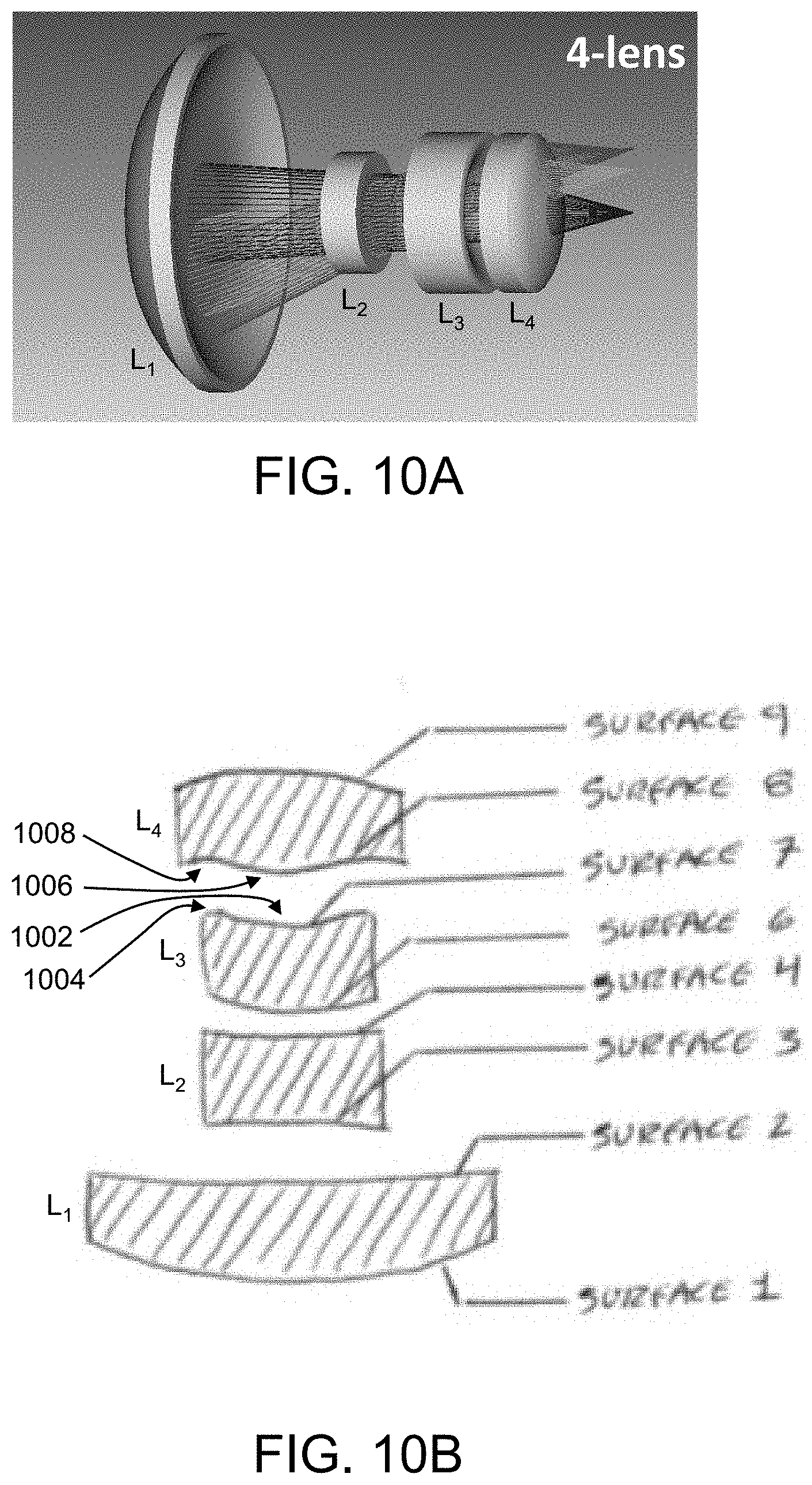
[0067] FIGS. 10A and 10B illustrate an example second set of lens elements L.sub.1, L.sub.2, L.sub.3, and L.sub.4 that may be included in the zoom lens assembly of FIG. 1, arranged in accordance with at least one embodiment described herein. In particular, FIG. 10A illustrates a rear and right side perspective view of the second set of lens elements and FIG. 10B illustrates a cross-sectional side view of the second set of lens elements. The second set of lens elements have a different relative spacing in FIG. 10A than in FIG. 10B, which may be achieved by moving one or more of the lens elements axially relative to the other lens elements and/or relative to an image sensor (not shown, but may be located where the example light rays in FIG. 10A are focused).
[0068] As illustrated in FIGS. 10A and 10B, each of the lens elements is an aspheric lens element.
[0069] The first and fourth lens elements L.sub.1 and L.sub.4 may be referred to as end lens elements. The second and third lens elements L.sub.2 and L.sub.3 may be referred to as intermediate lens elements.
[0070] The input surface of the first lens element L.sub.1, labeled "SURFACE 1" in FIG. 10B, may be convex. The output surface of the first lens element L.sub.1, labeled "SURFACE 2" in FIG. 2C, may be concave, or substantially concave. Thus, the first lens element L.sub.1 may be or may substantially be a meniscus lens element, and in particular a positive meniscus lens element.
[0071] The second lens elements L.sub.2 may be a biconcave lens element. For example, the input surface of the second lens element L.sub.2, labeled "SURFACE 3" in FIG. 10B, may be concave. Similarly, the output surface of the second lens element L.sub.2, labeled "SURFACE 4" in FIG. 10B, may be concave.
[0072] The input surface of the third lens element L.sub.3, labeled "SURFACE 6" in FIG. 10B, may be convex. The output surface of the third lens element L.sub.3, labeled "SURFACE 7" in FIG. 10B, includes a central portion 1002 (FIG. 10B) with a concave curvature, surrounded by a ring portion 1004 (FIG. 10B) with a convex curvature.
[0073] The input surface of the fourth lens element L.sub.4, labeled "SURFACE 8" in FIG. 10B, includes a central portion 1006 (FIG. 10B) with a convex curvature surrounded by a ring portion 1008 (FIG. 10B) with a concave curvature. The output surface of the fourth lens element L.sub.4, labeled "SURFACE 9" in FIG. 10B, may be convex.
[0074] In some embodiments, the surface sag of the lens elements of FIGS. 10A and 10B may be described by an nth order polynomial. In an example, the surface sag z(r) of the lens elements of FIGS. 10A and 10B may be described particularly by equation 1, reproduced here:
z = cr 2 1 + 1 - ( 1 + k ) c 2 r 2 + .alpha. 1 r 2 + .alpha. 2 r 4 + .alpha. 3 r 6 + .alpha. 4 r 8 + .alpha. 5 r 10 + .alpha. 6 r 12 + .alpha. 7 r 14 + .alpha. 8 r 16 ##EQU00002##
Optical polymer E48R, COP, or other suitable material may be used as lens material for each of the lens elements of FIGS. 10A and 10B.
[0075] Tables 2.1, 2.2, and 2.3 below (hereinafter collectively "Table 2") define the size, surface shape (in connection with equation 1--see above), and other parameters of the lens elements of FIGS. 10A and 10B, arranged in accordance with at least one embodiment described herein. In the surface data summary (Table 2.1), optical media are cascaded one after another: if the Glass type of a surface is E48R, it means this surface is followed by the medium E48R (i.e., front surface of a lens); if the Glass type is Air, it means this surface is followed by air (i.e., back surface of a lens or an air gap). In addition, aspherical surfaces are designated as EVENASPH. For each design, also listed (in Table 2.3) are the variable air-gap thicknesses between lenses at different configurations (i.e., zoom ratios). In Table 2.3, "Thickness 2" may refer to the variable air-gap thickness between the first and second lens elements L.sub.1 and L.sub.2, "Thickness 3" may refer to the variable air-gap thickness between the second lens element L.sub.2 and the lens stop ("STO" in Table 2) of the lens elements, "Thickness 5" may refer to the variable air-gap thickness between the lens stop and the third lens element L.sub.3, "Thickness 7" may refer to the variable air-gap thickness between the third and fourth lens elements L.sub.3 and L.sub.4, and "Thickness 9" may refer to the variable air-gap thickness between the fourth lens element L.sub.3 and the image sensor. The lens parameters and thicknesses may be fixed across different configurations.
[0076] In more detail, Table 2.1 below includes a summary of various aspects of the lens elements of FIGS. 2A in accordance with at least one embodiment described herein. In Table 2.1, OBJ refers to object, STO refers to lens stop (or the overall aperture of the system), and IMA refers to image.
TABLE-US-00004 TABLE 2.1 SURFACE DATA SUMMARY: Surf Type Radius Thickness Glass Diameter Conic OBJ STANDARD Infinity Infinity 0 0 1 EVENASPH 4.966542 0.8736672 E48R 3.519654 2.792135 2 EVENASPH 58.50144 0.4911522 air 3.294412 -15895.84 3 EVENASPH -10.23674 0.7929387 E48R 1.555136 -126.0018 4 EVENASPH -8.11578 8.1212952 air 1.087968 -6.240555e+039 STO STANDARD Infinity 0.0552063 air 1.067124 0 6 EVENASPH 1.682407 0.7531906 E48R 1.431985 -8.713099 7 EVENASPH 1.526977 0.4960468 air 1.435466 1.343006 8 EVENASPH 1.885781 0.8618348 E48R 1.650513 -9.524917 9 EVENASPH -2.384368 2.763117 air 1.947863 -9.905843e+039 IMA STANDARD Infinity 2.773127 0
[0077] Table 2.2 below includes details of the lens elements of FIGS. 10A and 10B defined according to equation 1 in accordance with at least one embodiment described herein. In Table 2.2, "Coefficient on r.LAMBDA.2" for a given surface refers to the aspheric coefficient a.sub.1 in equation 1 for the surface, "Coefficient on r.LAMBDA.4" for a given surface refers to the aspheric coefficient .alpha..sub.2 in equation 1 for the surface, "Coefficient on r.LAMBDA.6" for a given surface refers to the aspheric coefficient .alpha..sub.2 in equation 1 for the surface, and so on.
TABLE-US-00005 TABLE 2.2 Surface OBJ STANDARD Surface 1 EVENASPH Coefficient on r{circumflex over ( )} 2: -0.0012638346 Coefficient on r{circumflex over ( )} 4: -0.007714132 Coefficient on r{circumflex over ( )} 6: 0.0070802662 Coefficient on r{circumflex over ( )} 8: -0.0019558739 Coefficient on r{circumflex over ( )} 10: 0.00029708677 Coefficient on r{circumflex over ( )} 12: -4.7532547e-005 Coefficient on r{circumflex over ( )} 14: 0 Coefficient on r{circumflex over ( )} 16: 0 Surface 2 EVENASPH Coefficient on r{circumflex over ( )} 2: 0.0014155116 Coefficient on r{circumflex over ( )} 4: 0.0016870772 Coefficient on r{circumflex over ( )} 6: 0.0050544592 Coefficient on r{circumflex over ( )} 8: 0.00066717251 Coefficient on r{circumflex over ( )} 10: -0.0009103397 Coefficient on r{circumflex over ( )} 12: 0.0001073435 Coefficient on r{circumflex over ( )} 14: 0 Coefficient on r{circumflex over ( )} 16: 0 Surface 3 EVENASPH Coefficient on r{circumflex over ( )} 2: -0.0075178763 Coefficient on r{circumflex over ( )} 4: 0.0543452 Coefficient on r{circumflex over ( )} 6: 0.064025185 Coefficient on r{circumflex over ( )} 8: -0.31547469 Coefficient on r{circumflex over ( )} 10: 0.46578681 Coefficient on r{circumflex over ( )} 12: -0.24071053 Coefficient on r{circumflex over ( )} 14: 0 Coefficient on r{circumflex over ( )} 16: 0 Surface 4 EVENASPH Coefficient on r{circumflex over ( )} 2: 0.01128493 Coefficient on r{circumflex over ( )} 4: 0.22305579 Coefficient on r{circumflex over ( )} 6: -1.8382321 Coefficient on r{circumflex over ( )} 8: 11.409779 Coefficient on r{circumflex over ( )} 10: -32.894142 Coefficient on r{circumflex over ( )} 12: 35.654119 Coefficient on r{circumflex over ( )} 14: 0 Coefficient on r{circumflex over ( )} 16: 0 Surface STO STANDARD Surface 6 EVENASPH Coefficient on r{circumflex over ( )} 2: 0.02635669 Coefficient on r{circumflex over ( )} 4: 0.027402855 Coefficient on r{circumflex over ( )} 6: -0.36886653 Coefficient on r{circumflex over ( )} 8: 1.2142254 Coefficient on r{circumflex over ( )} 10: -1.9956879 Coefficient on r{circumflex over ( )} 12: 1.2079426 Coefficient on r{circumflex over ( )} 14: 0 Coefficient on r{circumflex over ( )} 16: 0 Surface 7 EVENASPH Coefficient on r{circumflex over ( )} 2: 0.16187438 Coefficient on r{circumflex over ( )} 4: -0.58900394 Coefficient on r{circumflex over ( )} 6: 0.16119593 Coefficient on r{circumflex over ( )} 8: -0.069044756 Coefficient on r{circumflex over ( )} 10: -0.13161956 Coefficient on r{circumflex over ( )} 12: 0.15102688 Coefficient on r{circumflex over ( )} 14: 0 Coefficient on r{circumflex over ( )} 16: 0 Surface 8 EVENASPH Coefficient on r{circumflex over ( )} 2: -0.043803586 Coefficient on r{circumflex over ( )} 4: 0.060486476 Coefficient on r{circumflex over ( )} 6: -0.35576092 Coefficient on r{circumflex over ( )} 8: 0.29031 Coefficient on r{circumflex over ( )} 10: -0.44034238 Coefficient on r{circumflex over ( )} 12: 0.37660628 Coefficient on r{circumflex over ( )} 14: 0 Coefficient on r{circumflex over ( )} 16: 0 Surface 9 EVENASPH Coefficient on r{circumflex over ( )} 2: -0.15673784 Coefficient on r{circumflex over ( )} 4: 0.034222678 Coefficient on r{circumflex over ( )} 6: -0.11761867 Coefficient on r{circumflex over ( )} 8: 0.050871983 Coefficient on r{circumflex over ( )} 10: -0.056151157 Coefficient on r{circumflex over ( )} 12: 0.051580637 Coefficient on r{circumflex over ( )} 14: 0 Coefficient on r{circumflex over ( )} 16: 0
[0078] Table 2.3 below includes details of the edge thickness of the surfaces of the lens elements of FIGS. 10A and 10B in accordance with at least one embodiment described herein. Table 2.3 also lists the variable air-gap thicknesses between lenses at different configurations (i.e., zoom ratios).
TABLE-US-00006 TABLE 2.3 DGE THICKNESS DATA: Surf Edge 1 0.588977 2 0.406558 3 0.817326 4 0.109266 STO 0.180929 6 0.768863 7 0.413722 8 0.620138 9 2.945744 IMA 0.000000 MULTI-CONFIGURATION DATA: Configuration 1: 1 Thickness 2: 0.4911522 Variable 2 Thickness 4: 0.1212952 Variable 3 Thickness 5: 0.0552063 Variable 4 Thickness 7: 0.4960468 Variable 5 Thickness 9: 2.763117 Variable Configuration 2: 1 Thickness 2: 4.283115 Variable 2 Thickness 4: 0.7223943 Variable 3 Thickness 5: 2.861504 Variable 4 Thickness 7: 0.5940857 Variable 5 Thickness 9: 1.255213 Variable Configuration 3: 1 Thickness 2: 2.819352 Variable 2 Thickness 4: 0.2887189 Variable 3 Thickness 5: 5.994817 Variable 4 Thickness 7: 0.8897799 Variable 5 Thickness 9: 1.725705 Variable
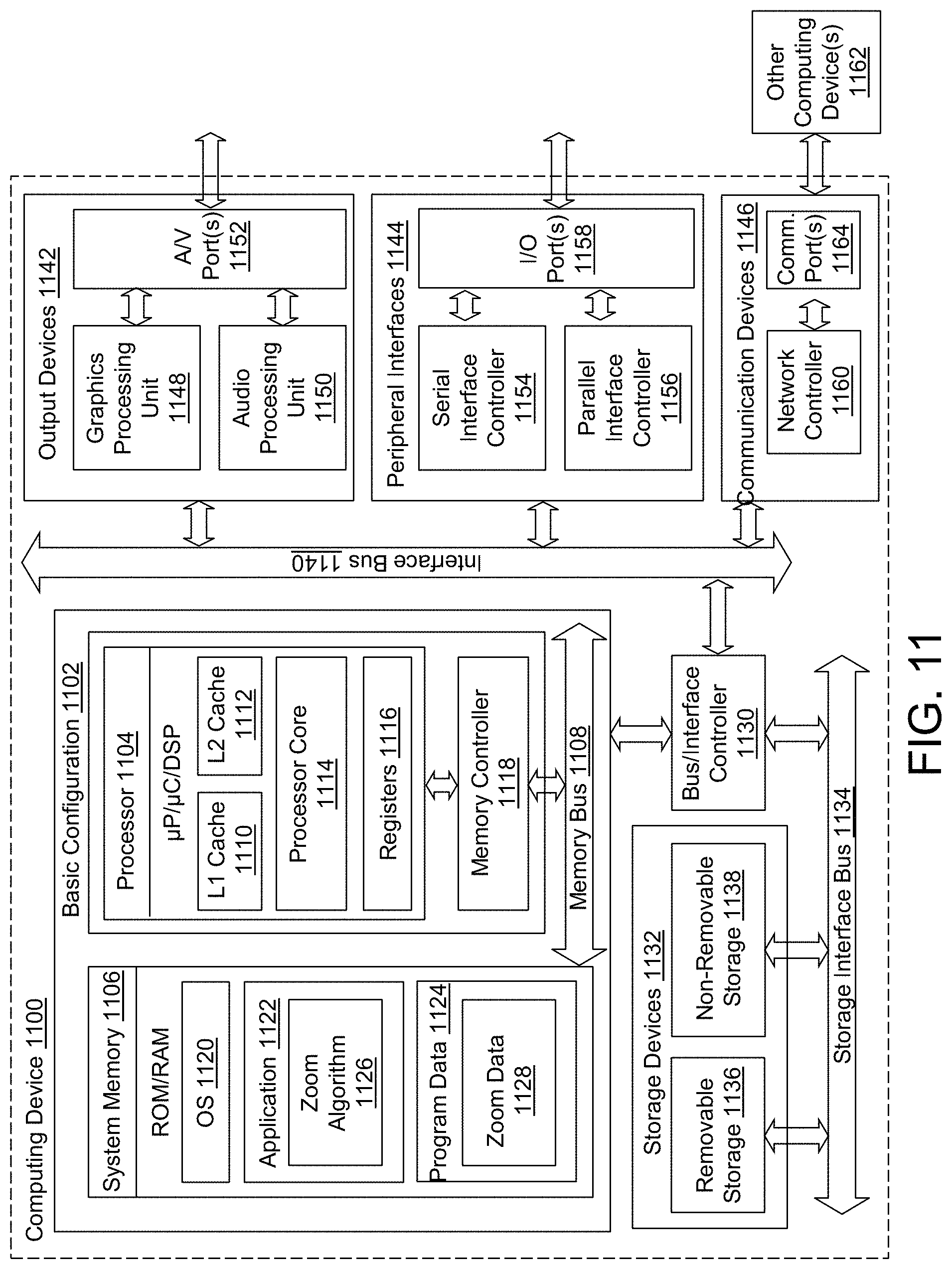
[0079] FIG. 11 illustrates a block diagram of an example computing device 1100, arranged in accordance with at least one embodiment described herein. The computing device 1100 may be used in some embodiments to perform or control performance of one or more of the methods and/or operations described herein. For instance, the computing device 1100 may be communicatively coupled to and/or included in the zoom lens assembly 100 described herein to perform or control performance of positional adjustments of lens elements to adjust the zoom and/or view angle of the zoom lens assembly 100. In a basic configuration 1102, the computing device 1100 typically includes one or more processors 1104 and a system memory 1106. A memory bus 1108 may be used for communicating between the processor 1104 and the system memory 1106.
[0080] Depending on the desired configuration, the processor 1104 may be of any type, such as a microprocessor (.mu.P), a microcontroller (.mu.C), a digital signal processor (DSP), or any combination thereof. The processor 1104 may include one or more levels of caching, such as a level one cache 1110 and a level two cache 1112, a processor core 1114, and registers 1116. The processor core 1114 may include an arithmetic logic unit (ALU), a floating point unit (FPU), a digital signal processing core (DSP Core), or any combination thereof. An example memory controller 1118 may also be used with the processor 1104, or in some implementations the memory controller 1118 may be an internal part of the processor 1104.
[0081] Depending on the desired configuration, the system memory 1106 may be of any type, such as volatile memory (such as RAM), non-volatile memory (such as ROM, flash memory, or the like), or any combination thereof. The system memory 1106 may include an operating system 1120, one or more applications 1122, and program data 1124. The application 1122 may include a zoom algorithm 1126 that is arranged to make positional adjustments of one or more lens elements in the zoom lens assembly 100. The program data 1124 may include zoom data 1128 such as axial positions of one or more of the lens elements of the zoom lens assembly 100 for one or more zoom ratios. In some embodiments, the application 1122 may be arranged to operate with the program data 1124 on the operating system 1120 to perform one or more of the methods and/or operations described herein.
[0082] The computing device 1100 may include additional features or functionality, and additional interfaces to facilitate communications between the basic configuration 1102 and any other devices and interfaces. For example, a bus/interface controller 1130 may be used to facilitate communications between the basic configuration 1102 and one or more data storage devices 1132 via a storage interface bus 1134. The data storage devices 1132 may include removable storage devices 1136, non-removable storage devices 1138, or a combination thereof. Examples of removable storage and non-removable storage devices include magnetic disk devices such as flexible disk drives and hard-disk drives (HDDs), optical disk drives such as compact disk (CD) drives or digital versatile disk (DVD) drives, solid state drives (SSDs), and tape drives to name a few. Example computer storage media may include volatile and nonvolatile, removable and non-removable media implemented in any method or technology for storage of information, such as computer-readable instructions, data structures, program modules, or other data.
[0083] The system memory 1106, the removable storage devices 1136, and the non-removable storage devices 1138 are examples of computer storage media. Computer storage media includes, but is not limited to, RAM, ROM, EEPROM, flash memory or other memory technology, CD-ROM, digital versatile disks (DVDs) or other optical storage, magnetic cassettes, magnetic tape, magnetic disk storage or other magnetic storage devices, or any other medium which may be used to store the desired information and which may be accessed by the computing device 1100. Any such computer storage media may be part of the computing device 1100.
[0084] The computing device 1100 may also include an interface bus 1140 for facilitating communication from various interface devices (e.g., output devices 1142, peripheral interfaces 1144, and communication devices 1146) to the basic configuration 1102 via the bus/interface controller 1130. The output devices 1142 include a graphics processing unit 1148 and an audio processing unit 1150, which may be configured to communicate to various external devices such as a display or speakers via one or more A/V ports 1152. The peripheral interfaces 1144 include a serial interface controller 1154 or a parallel interface controller 1156, which may be configured to communicate with external devices such as input devices (e.g., keyboard, mouse, pen, voice input device, touch input device, and/or others), sensors, or other peripheral devices (e.g., printer, scanner, and/or others) via one or more I/O ports 1158. The communication devices 1146 include a network controller 1160, which may be arranged to facilitate communications with one or more other computing devices 1162 over a network communication link via one or more communication ports 1164.
[0085] The network communication link may be one example of a communication media. Communication media may typically be embodied by computer-readable instructions, data structures, program modules, or other data in a modulated data signal, such as a carrier wave or other transport mechanism, and may include any information delivery media. A "modulated data signal" may be a signal that includes one or more of its characteristics set or changed in such a manner as to encode information in the signal. By way of example, and not limitation, communication media may include wired media such as a wired network or direct-wired connection, and wireless media such as acoustic, radio frequency (RF), microwave, infrared (IR), and other wireless media. The term "computer-readable media" as used herein may include both storage media and communication media.
[0086] The computing device 1100 may be implemented as a portion of a small-form factor portable (or mobile) electronic device such as a cell phone, a personal data assistant (PDA), a personal media player device, a wireless web-watch device, a personal headset device, an application-specific device, or a hybrid device that includes any of the above functions. The computing device 1100 may also be implemented as a personal computer including both laptop computer and non-laptop computer configurations.
[0087] Although the subject matter has been described in language specific to structural features and/or methodological acts, it is to be understood that the subject matter configured in the appended claims is not necessarily limited to the specific features or acts described above. Rather, the specific features and acts described above are disclosed as example forms of implementing the claims.
[0088] Unless specific arrangements described herein are mutually exclusive with one another, the various implementations described herein can be combined in whole or in part to enhance system functionality and/or to produce complementary functions. Likewise, aspects of the implementations may be implemented in standalone arrangements. Thus, the above description has been given by way of example only and modification in detail may be made within the scope of the present invention.
[0089] With respect to the use of substantially any plural or singular terms herein, those having skill in the art can translate from the plural to the singular or from the singular to the plural as is appropriate to the context or application. The various singular/plural permutations may be expressly set forth herein for sake of clarity. A reference to an element in the singular is not intended to mean "one and only one" unless specifically stated, but rather "one or more." Moreover, nothing disclosed herein is intended to be dedicated to the public regardless of whether such disclosure is explicitly recited in the above description.
[0090] In general, terms used herein, and especially in the appended claims (e.g., bodies of the appended claims) are generally intended as "open" terms (e.g., the term "including" should be interpreted as "including but not limited to," the term "having" should be interpreted as "having at least," the term "includes" should be interpreted as "includes but is not limited to," etc.). Furthermore, in those instances where a convention analogous to "at least one of A, B, and C, etc." is used, in general, such a construction is intended in the sense one having skill in the art would understand the convention (e.g., "a system having at least one of A, B, and C" would include but not be limited to systems that include A alone, B alone, C alone, A and B together, A and C together, B and C together, or A, B, and C together, etc.). Also, a phrase presenting two or more alternative terms, whether in the description, claims, or drawings, should be understood to include one of the terms, either of the terms, or both terms. For example, the phrase "A or B" will be understood to include the possibilities of "A" or "B" or "A and B."
[0091] The present invention may be embodied in other specific forms without departing from its spirit or essential characteristics. The described implementations are to be considered in all respects only as illustrative and not restrictive. The scope of the invention is, therefore, indicated by the appended claims rather than by the foregoing description. All changes which come within the meaning and range of equivalency of the claims are to be embraced within their scope.
* * * * *
D00000
D00001
D00002
D00003
D00004
D00005
D00006
D00007
D00008
D00009
D00010
D00011
D00012

D00013
D00014
D00015


XML
uspto.report is an independent third-party trademark research tool that is not affiliated, endorsed, or sponsored by the United States Patent and Trademark Office (USPTO) or any other governmental organization. The information provided by uspto.report is based on publicly available data at the time of writing and is intended for informational purposes only.
While we strive to provide accurate and up-to-date information, we do not guarantee the accuracy, completeness, reliability, or suitability of the information displayed on this site. The use of this site is at your own risk. Any reliance you place on such information is therefore strictly at your own risk.
All official trademark data, including owner information, should be verified by visiting the official USPTO website at www.uspto.gov. This site is not intended to replace professional legal advice and should not be used as a substitute for consulting with a legal professional who is knowledgeable about trademark law.