3d Microdisplay Device And Structure
A1
U.S. patent application number 16/860027 was filed with the patent office on 2020-08-13 for 3d microdisplay device and structure. This patent application is currently assigned to Monolithic 3D Inc.. The applicant listed for this patent is Monolithic 3D Inc.. Invention is credited to Zvi Or-Bach, Deepak C. Sekar.
| Application Number | 20200259048 16/860027 |
| Document ID | 20200259048 / US20200259048 |
| Family ID | 1000004807877 |
| Filed Date | 2020-08-13 |
| Patent Application | download [pdf] |


View All Diagrams
| United States Patent Application | 20200259048 |
| Kind Code | A1 |
| Or-Bach; Zvi ; et al. | August 13, 2020 |
3D MICRODISPLAY DEVICE AND STRUCTURE
Abstract
A 3D micro display, the 3D micro display including: a first single crystal layer including at least one LED driving circuit; a second single crystal layer including a first plurality of light emitting diodes (LEDs), where the second single crystal layer is on top of the first single crystal layer, where the second single crystal layer includes at least ten individual first LED pixels; and a second plurality of light emitting diodes (LEDs), where the 3D micro display includes an oxide to oxide bonding structure.
| Inventors: | Or-Bach; Zvi; (San Jose, CA) ; Sekar; Deepak C.; (San Jose, CA) | ||||||||||
| Applicant: |
|
||||||||||
|---|---|---|---|---|---|---|---|---|---|---|---|
| Assignee: | Monolithic 3D Inc. San Jose CA |
||||||||||
| Family ID: | 1000004807877 | ||||||||||
| Appl. No.: | 16/860027 | ||||||||||
| Filed: | April 27, 2020 |
Related U.S. Patent Documents
| Application Number | Filing Date | Patent Number | ||
|---|---|---|---|---|
| 15920499 | Mar 14, 2018 | 10679977 | ||
| 16860027 | ||||
| 14936657 | Nov 9, 2015 | 9941319 | ||
| 15920499 | ||||
| 13274161 | Oct 14, 2011 | 9197804 | ||
| 14936657 | ||||
| 12904103 | Oct 13, 2010 | 8163581 | ||
| 13274161 | ||||
| Current U.S. Class: | 1/1 |
| Current CPC Class: | H01L 27/15 20130101; G09G 3/32 20130101; H01L 33/24 20130101; H01L 33/504 20130101; G02B 30/50 20200101 |
| International Class: | H01L 33/24 20060101 H01L033/24; H01L 27/15 20060101 H01L027/15; G09G 3/32 20060101 G09G003/32; H01L 33/50 20060101 H01L033/50; G02B 30/50 20060101 G02B030/50 |
Claims
1. A 3D micro display, the 3D micro display comprising: a first single crystal layer comprising at least one LED driving circuit; a second single crystal layer comprising a first plurality of light emitting diodes (LEDs), wherein said second single crystal layer is on top of said first single crystal layer, wherein said second single crystal layer comprises at least ten individual first LED pixels; and a second plurality of light emitting diodes (LEDs), wherein said 3D micro display comprises an oxide to oxide bonding structure.
2. The 3D micro display according to claim 1, wherein a plurality of said first LED pixels are individually driven, each by a said LED driving circuit, and wherein said second single crystal layer and said first single crystal layer are separated by a vertical distance of less than ten microns.
3. The 3D micro display according to claim 1, further comprising: a top surface of said first single crystal layer; and a bottom surface of said second single crystal layer, wherein said vertical distance is the distance from said top surface of said first single crystal layer to said bottom surface of said second single crystal layer.
4. The 3D micro display according to claim 1, further comprising: a third single crystal layer, wherein said third single crystal layer overlays said second single crystal layer.
5. The 3D micro display according to claim 1, wherein said first plurality of light emitting diodes (LEDs) emits a first light with a first wavelength, wherein said second plurality of light emitting diodes (LEDs) emits a second light with a second wavelength, and wherein said first wavelength and said second wavelength differ by greater than 10 nm.
6. The 3D micro display according to claim 1, further comprising: a third single crystal layer, wherein said third single crystal layer comprises at least ten second LED pixels.
7. A 3D micro display, the 3D micro display comprising: a first single crystal layer comprising at least one LED driving circuit; a second single crystal layer comprising a first plurality of light emitting diodes (LEDs), wherein said second single crystal layer is on top of said first single crystal layer, wherein said second single crystal layer comprises at least ten individual first LED pixels; a second plurality of light emitting diodes (LEDs); and a third single crystal layer, wherein said third single crystal layer is on top of said second single crystal layer, and wherein said LED driving circuit comprises n type devices and p type devices.
8. The 3D micro display according to claim 7, wherein a plurality of said first LED pixels are individually driven, each by a said LED driving circuit.
9. The 3D micro display according to claim 7, wherein said second single crystal layer and said first single crystal layer are separated by a vertical distance of less than ten microns.
10. The 3D micro display according to claim 7, a top surface of said first single crystal layer; and a bottom surface of said second single crystal layer, wherein a vertical distance is a distance from said top surface of said first single crystal layer to said bottom surface of said second single crystal layer, and wherein said vertical distance is less than ten microns.
11. The 3D micro display according to claim 7, wherein said first plurality of light emitting diodes (LEDs) emits a first light with a first wavelength, wherein said second plurality of light emitting diodes (LEDs) emits a second light with a second wavelength, and wherein said first wavelength and said second wavelength differ by greater than 10 nm.
12. The 3D micro display according to claim 7, wherein said third single crystal layer comprises at least ten individual second LED pixels.
13. The 3D micro display according to claim 7, further comprising: a fourth single crystal layer, wherein said fourth single crystal layer is on top of said third single crystal layer.
14. A 3D micro display, the 3D micro display comprising: a first single crystal layer comprising at least one LED driving circuit; a second single crystal layer comprising a first plurality of light emitting diodes (LEDs), wherein said second single crystal layer is on top of said first single crystal layer, wherein said second single crystal layer comprises at least ten individual first LED pixels; and a second plurality of light emitting diodes (LEDs), wherein said first plurality of light emitting diodes (LEDs) emits a first light with a first wavelength, wherein said second plurality of light emitting diodes (LEDs) emits a second light with a second wavelength, wherein said first wavelength and said second wavelength differ by greater than 10 nm, and wherein said 3D micro display comprises an oxide to oxide bonding structure.
15. The 3D micro display according to claim 14, wherein a plurality of said first LED pixels are individually driven, each by a said LED driving circuit.
16. The 3D micro display according to claim 14, wherein said second single crystal layer and said first single crystal layer are separated by a vertical distance of less than ten microns.
17. The 3D micro display according to claim 14, further comprising: a top surface of said first single crystal layer; and a bottom surface of said second single crystal layer, wherein a vertical distance is a distance from said top surface of said first single crystal layer to said bottom surface of said second single crystal layer, and wherein said vertical distance is less than ten microns.
18. The 3D micro display according to claim 14, further comprising: a third plurality of light emitting diodes (LEDs), wherein said third plurality of light emitting diodes (LED) emits a third light with a third wavelength, and wherein said first wavelength and said second wavelength and said third wavelength differ by greater than 10 nm from each other.
19. The 3D micro display according to claim 14, further comprising: a third single crystal layer, wherein said third single crystal layer is on top of said second single crystal layer, and wherein said third single crystal layer comprises at least ten second LED pixels.
20. The 3D micro display according to claim 14, further comprising: a third single crystal layer, wherein said third single crystal layer is on top of said second single crystal layer, and wherein said third single crystal layer comprises at least ten second LED pixels; and a fourth single crystal layer, wherein said fourth single crystal layer is on top of said third single crystal layer.
Description
CROSS-REFERENCE OF RELATED APPLICATION
[0001] This application is a continuation-in-part of U.S. patent application Ser. No. 15/920,499 filed on Mar. 14, 2018; which is a continuation-in-part of U.S. patent application Ser. No. 14/936,657 filed on Nov. 9, 2015, now U.S. Pat. No. 9,941,319 issued on Apr. 10, 2018; which is a continuation-in-part of U.S. patent application Ser. No. 13/274,161 filed on Oct. 14, 2011, now U.S. Pat. No. 9,197,804 issued on Nov. 24, 2015; and this application is a continuation-in-part of U.S. patent application Ser. No. 12/904,103 filed on Oct. 13, 2011, now U.S. Pat. No. 8,163,581 issued on Apr. 24, 2012; the entire contents of all of the preceding are incorporated herein by reference.
BACKGROUND OF THE INVENTION
(A) Field of the Invention
[0002] This invention describes applications of monolithic 3D integration to various disciplines, including but not limited to, for example, light-emitting diodes, displays, image-sensors and solar cells.
(B) Discussion of Background Art
[0003] Semiconductor and optoelectronic devices often require thin monocrystalline (or single-crystal) films deposited on a certain wafer. To enable this deposition, many techniques, generally referred to as layer transfer technologies, have been developed. These include: [0004] Ion-cut, variations of which are referred to as smart-cut, nano-cleave and smart-cleave:
[0005] Further information on ion-cut technology is given in "Frontiers of silicon-on-insulator," J. Appl. Phys. 93, 4955-4978 (2003) by G. K. Celler and S. Cristolovean ("Celler") and also in "Mechanically induced Si layer transfer in hydrogen-implanted Si wafers," Appl. Phys. Lett., vol. 76, pp. 2370-2372, 2000 by K. Henttinen, I. Suni, and S. S. Lau ("Hentinnen"). [0006] Porous silicon approaches such as ELTRAN: These are described in "Eltran, Novel SOI Wafer Technology", JSAP International, Number 4, July 2001 by T. Yonehara and K. Sakaguchi ("Yonehara"). [0007] Lift-off with a temporary substrate, also referred to as epitaxial lift-off This is described in "Epitaxial lift-off and its applications", 1993 Semicond. Sci. Technol. 8 1124 by P. Demeester, et al ("Demeester"). [0008] Bonding a substrate with single crystal layers followed by Polishing, Time-controlled etch-back or Etch-stop layer controlled etch-back to thin the bonded substrate: These are described in U.S. Pat. No. 6,806,171 by A. Ulyashin and A. Usenko ("Ulyashin") and "Enabling SOI-Based Assembly Technology for Three-Dimensional (3D) Integrated Circuits (ICs)," IEDM Tech. Digest, p. 363 (2005) by A. W. Topol, D. C. La Tulipe, L. Shi, S. M. Alam, D. J. Frank, S. E. Steen, J. Vichiconti, D. Posillico, M. Cobb, S. Medd, J. Patel, S. Goma, D. DiMilia, M. T. Robson, E. Duch, M. Farinelli, C. Wang, R. A. Conti, D. M. Canaperi, L. Deligianni, A. Kumar, K. T. Kwietniak, C. D'Emic, J. Ott, A. M. Young, K. W. Guarini, and M. Ieong ("Topol"). [0009] Bonding a wafer with a Gallium Nitride film epitaxially grown on a sapphire substrate followed by laser lift-off for removing the transparent sapphire substrate: This method may be suitable for deposition of Gallium Nitride thin films, and is described in U.S. Pat. No. 6,071,795 by Nathan W. Cheung, Timothy D. Sands and William S. Wong ("Cheung"). [0010] Rubber stamp layer transfer: This is described in "Solar cells sliced and diced", 19 May 2010, Nature News. With novel applications of these methods and recognition of their individual strengths and weaknesses, one can significantly enhance today's light-emitting diode (LED), display, image-sensor and solar cell technologies.
Background on LEDs
[0011] Light emitting diodes (LEDs) are used in many applications, including automotive lighting, incandescent bulb replacements, and as backlights for displays. Red LEDs are typically made on Gallium Arsenide (GaAs) substrates, and include quantum wells constructed of various materials such as AlInGaP and GaInP. Blue and green LEDs are typically made on Sapphire or Silicon Carbide (SiC) or bulk Gallium Nitride (GaN) substrates, and include quantum wells constructed of various materials such as GaN and InGaN.
[0012] A white LED for lighting and display applications can be constructed by either using a blue LED coated with phosphor (called phosphor-coated LED or pcLED) or by combining light from red, blue, and green LEDs (called RGB LED). RGB LEDs are typically constructed by placing red, blue, and green LEDs side-by-side. While RGB LEDs are more energy-efficient than pcLEDs, they are less efficient in mixing red, blue and green colors to form white light. They also are much more costly than pcLEDs. To tackle issues with RGB LEDs, several proposals have been made.
[0013] One RGB LED proposal from Hong Kong University is described in "Design of vertically stacked polychromatic light emitting diodes", Optics Express, June 2009 by K. Hui, X. Wang, et al ("Hui"). It involves stacking red, blue, and green LEDs on top of each other after individually packaging each of these LEDs. While this solves light mixing problems, this RGB-LED is still much more costly than a pcLED solution since three LEDs for red, blue, and green color need to be packaged. A pcLED, on the other hand, requires just one LED to be packaged and coated with phosphor.
[0014] Another RGB LED proposal from Nichia Corporation is described in "Phosphor Free High-Luminous-Efficiency White Light-Emitting Diodes Composed of InGaN Multi-Quantum Well", Japanese Journal of Applied Physics, 2002 by M. Yamada, Y. Narukawa, et al. ("Yamada"). It involves constructing and stacking red, blue and green LEDs of GaN-based materials on a sapphire or SiC substrate. However, red LEDs are not efficient when constructed with GaN-based material systems, and that hampers usefulness of this implementation. It is not possible to deposit defect-free AlInGaP/InGaP for red LEDs on the same substrate as GaN based blue and green LEDs, due to a mismatch in thermal expansion co-efficient between the various material systems.
[0015] Yet another RGB-LED proposal is described in "Cascade Single chip phosphor-free while light emitting diodes", Applied Physics Letters, 2008 by X. Guo, G. Shen, et al. ("Guo"). It involves bonding GaAs based red LEDs with GaN based blue-green LEDs to produce white light. Unfortunately, this bonding process requires 600.degree. C. temperatures, causing issues with mismatch of thermal expansion co-efficients and cracking. Another publication on this topic is "A trichromatic phosphor-free white light-emitting diode by using adhesive bonding scheme", Proc. SPIE, Vol. 7635, 2009 by D. Chuai, X. Guo, et al. ("Chuai"). It involves bonding red LEDs with green-blue LED stacks. Bonding is done at the die level after dicing, which is more costly than a wafer-based approach.
[0016] U.S. patent application Ser. No. 12/130824 describes various stacked RGB LED devices. It also briefly mentions a method for construction of a stacked LED where all layers of the stacked LED are transferred using lift-off with a temporary carrier and Indium Tin Oxide (ITO) to semiconductor bonding. This method has several issues for constructing a RGB LED stack. First, it is difficult to manufacture a lift-off with a temporary carrier of red LEDs for producing a RGB LED stack, especially for substrates larger than 2 inch. This is because red LEDs are typically constructed on non-transparent GaAs substrates, and lift-off with a temporary carrier is done by using an epitaxial lift-off process. Here, the thin film to be transferred typically sits atop a "release-layer" (eg. AlAs), this release layer is removed by etch procedures after the thin film is attached to a temporary substrate. Scaling this process to 4 inch wafers and bigger is difficult. Second, it is very difficult to perform the bonding of ITO to semiconductor materials of a LED layer at reasonable temperatures, as described in the patent application Ser. No. 12/130824.
[0017] It is therefore clear that a better method for constructing RGB LEDs will be helpful. Since RGB LEDs are significantly more efficient than pcLEDs, they can be used as replacements of today's phosphor-based LEDs for many applications, provided a cheap and effective method of constructing RGB LEDs can be invented.
Background on Image-Sensors:
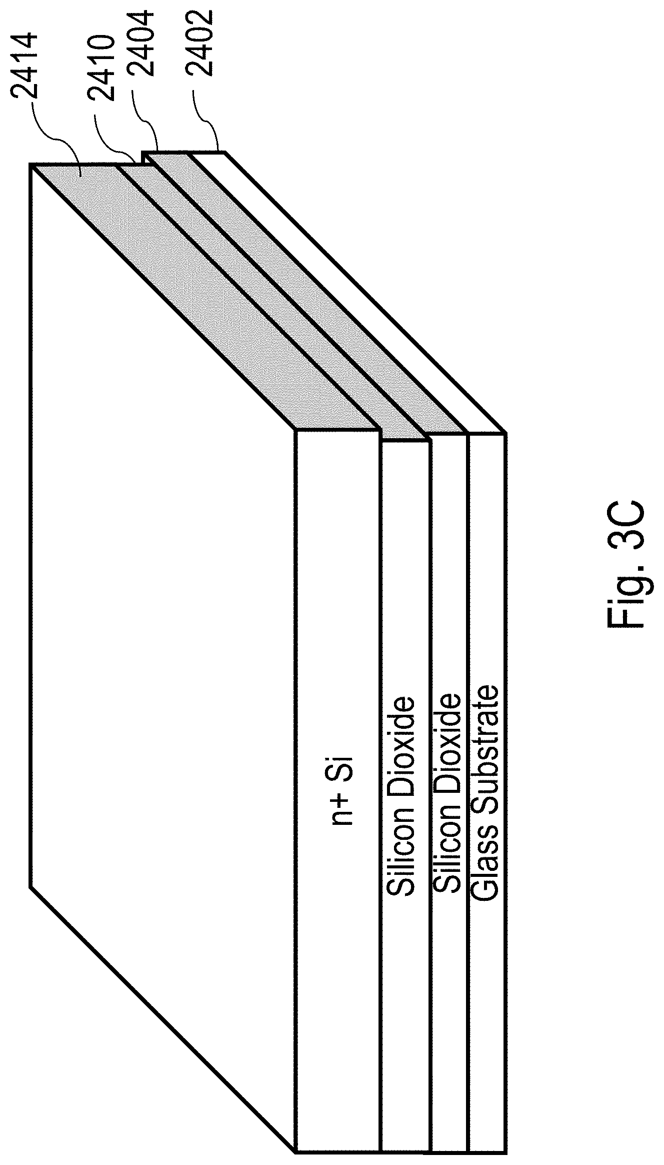
[0018] Image sensors are used in applications such as cameras. Red, blue, and green components of the incident light are sensed and stored in digital format. CMOS image sensors typically contain a photodetector and sensing circuitry. Almost all image sensors today have both the photodetector and sensing circuitry on the same chip. Since the area consumed by the sensing circuits is high, the photodetector cannot see the entire incident light, and image capture is not as efficient.
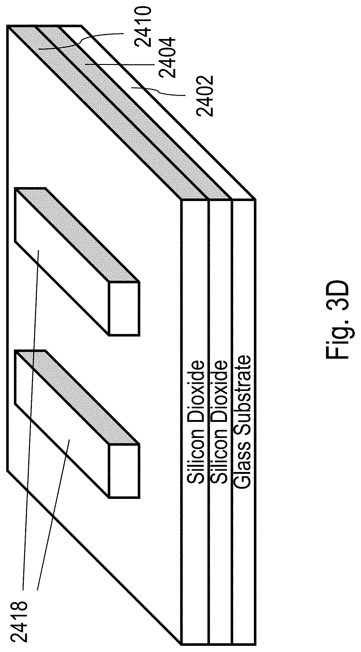
[0019] To tackle this problem, several researchers have proposed building the photodetectors and the sensing circuitry on separate chips and stacking them on top of each other. A publication that describes this method is "Megapixel CMOS image sensor fabricated in three-dimensional integrated circuit technology", Intl. Solid State Circuits Conference 2005 by Suntharalingam, V., Berger, R., et al. ("Suntharalingam"). These proposals use through-silicon via (TSV) technology where alignment is done in conjunction with bonding. However, pixel size is reaching the 1p.m range, and successfully processing TSVs in the 1 .mu.m range or below is very difficult. This is due to alignment issues while bonding. For example, the International Technology Roadmap for Semiconductors (ITRS) suggests that the 2-4 um TSV pitch will be the industry standard until 2012. A 2-4 .mu.m pitch TSV will be too big for a sub-1 .mu.m pixel. Therefore, novel techniques of stacking photodetectors and sensing circuitry are required.
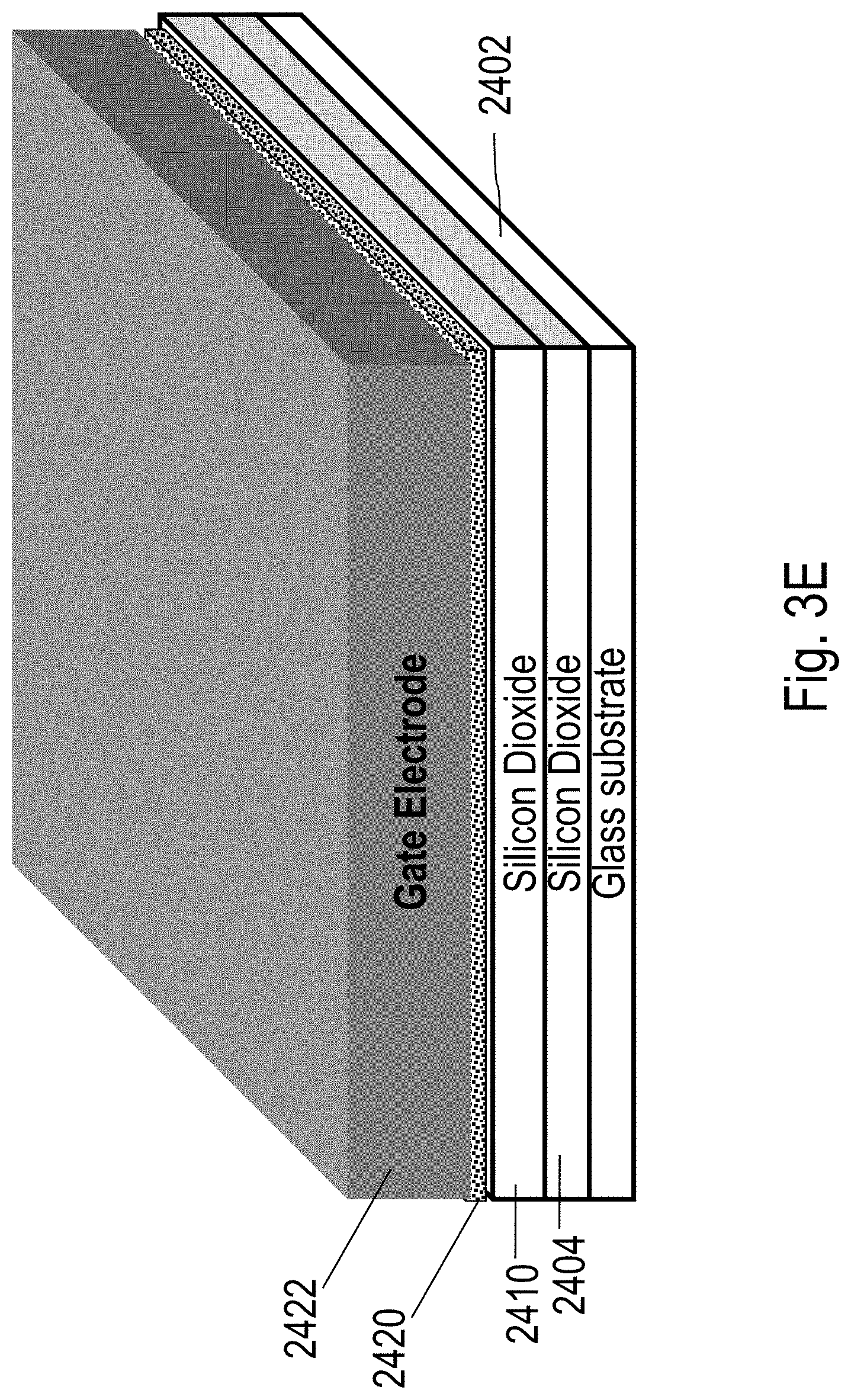
[0020] A possible solution to this problem is given in "Setting up 3D Sequential Integration for Back-Illuminated CMOS Image Sensors with Highly Miniaturized Pixels with Low Temperature Fully-depleted SOI Transistors," IEDM, p.1-4 (2008) by P. Coudrain et al. ("Coudrain"). In the publication, transistors are monolithically integrated on top of photodetectors. Unfortunately, transistor process temperatures reach 600.degree. C. or more. This is not ideal for transistors (that require a higher thermal budget) and photodetectors (that may prefer a lower thermal budget).
Background on Displays:
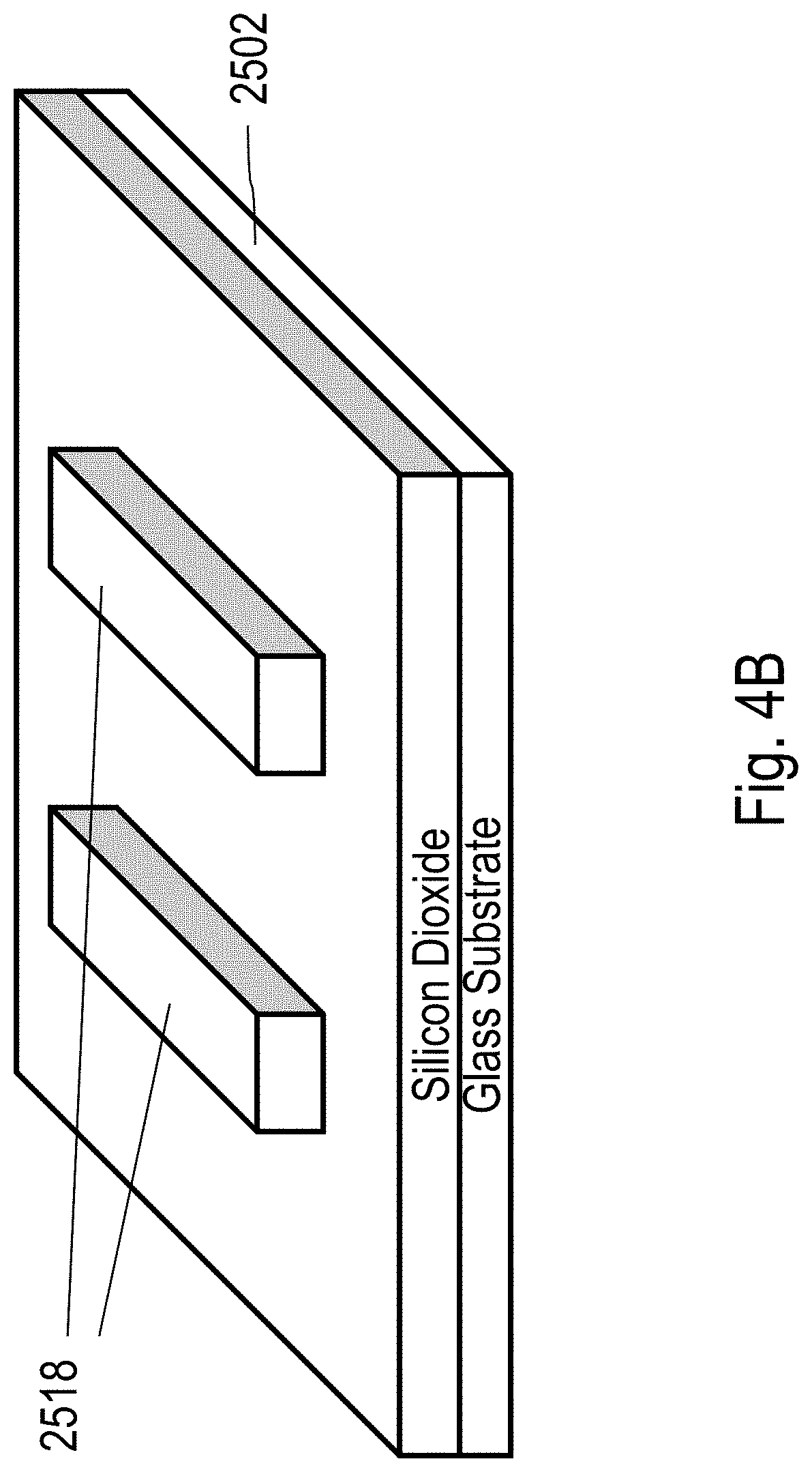
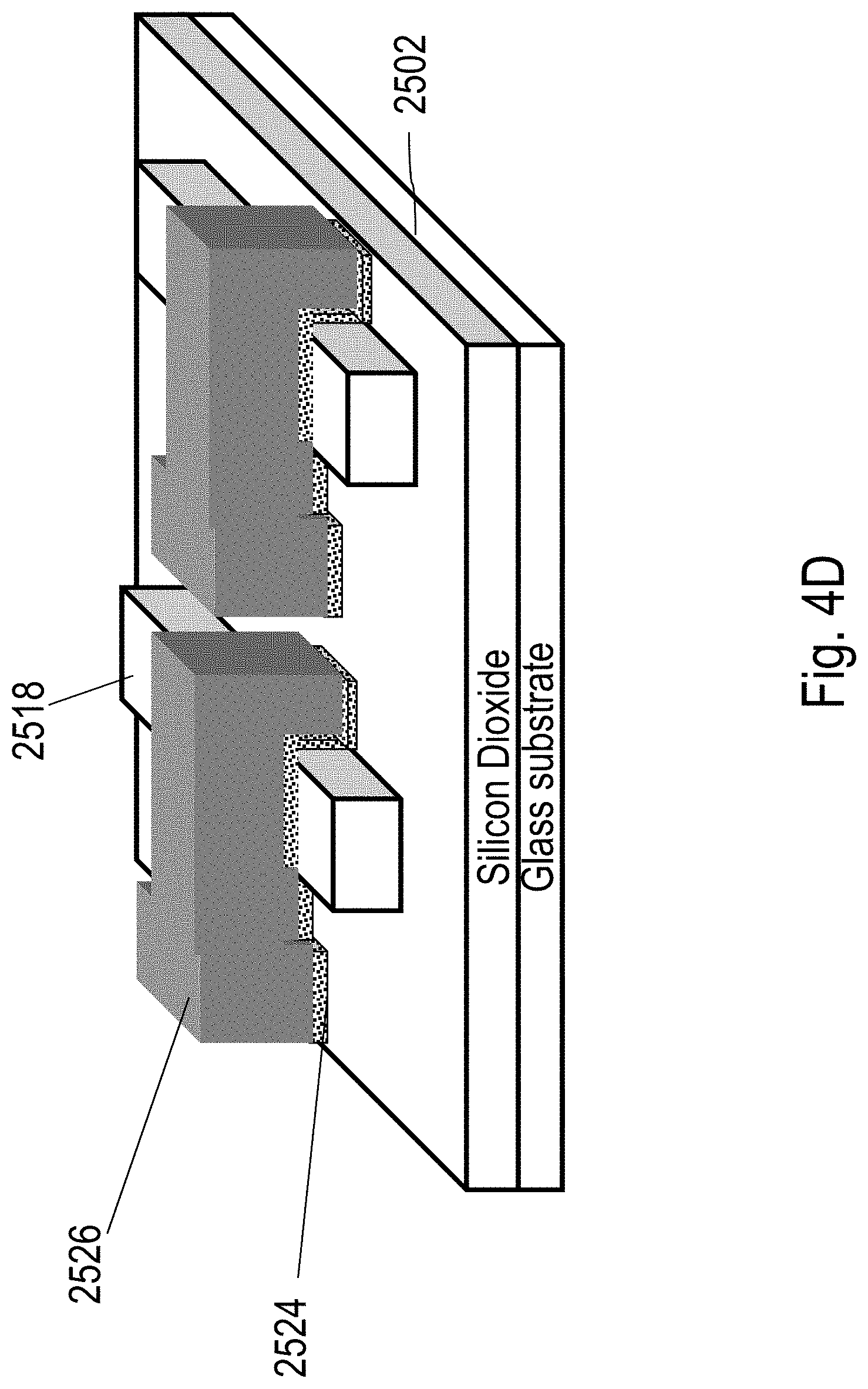
[0021] Liquid Crystal Displays (LCDs) can be classified into two types based on manufacturing technology utilized: (1) Large-size displays that are made of amorphous/polycrystalline silicon thin-film-transistors (TFTs), and (2) Microdisplays that utilize single-crystal silicon transistors. Microdisplays are typically used where very high resolution is needed, such as camera/camcorder view-finders, projectors and wearable computers.
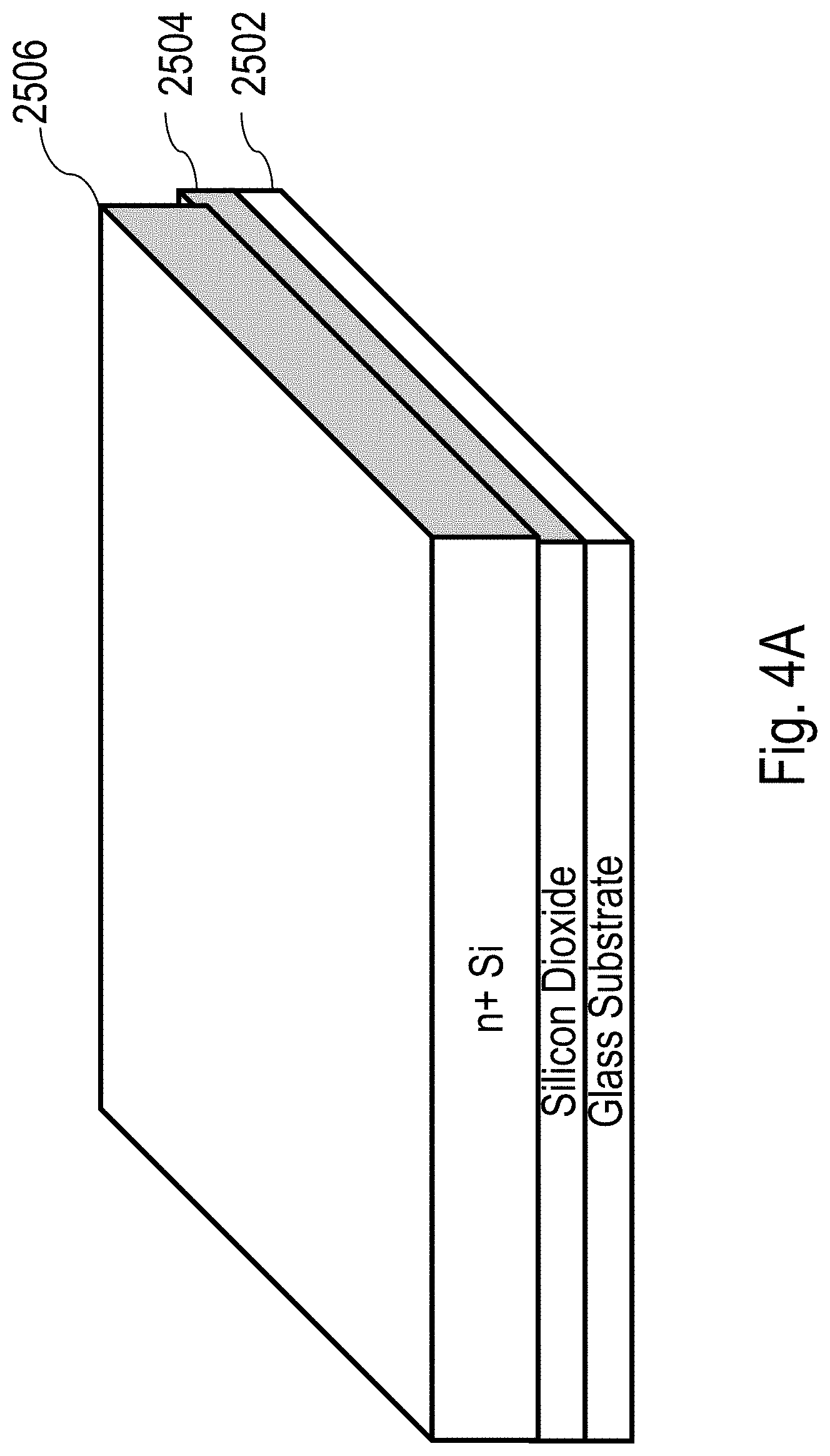
[0022] Microdisplays are made in semiconductor fabs with 200 mm or 300 mm wafers. They are typically constructed with LCOS (Liquid-Crystal-on-Silicon) Technology and are reflective in nature. An exception to this trend of reflective microdisplays is technology from Kopin Corporation (U.S. Pat. 5,317,236, filed December 1991). This company utilizes transmittive displays with a lift-off layer transfer scheme. Transmittive displays may be generally preferred for various applications.
[0023] While lift-off layer transfer schemes are viable for transmittive displays, they are frequently not used for semiconductor manufacturing due to yield issues. Therefore, other layer transfer schemes will be helpful. However, it is not easy to utilize other layer transfer schemes for making transistors in microdisplays. For example, application of "smart-cut" layer transfer to attach monocrystalline silicon transistors to glass is described in "Integration of Single Crystal Si TFTs and Circuits on a Large Glass Substrate", IEDM 2009 by Y. Takafuji, Y. Fukushima, K. Tomiyasu, et al. ("Takafuji"). Unfortunately, hydrogen is implanted through the gate oxide of transferred transistors in the process, and this degrades performance. Process temperatures are as high as 600.degree. C. in this paper, and this requires costly glass substrates. Several challenges therefore need to be overcome for efficient layer transfer, and require innovation.
Background on Solar Cells:
[0024] Solar cells can be constructed of several materials such as, for example, silicon and compound semiconductors. The highest efficiency solar cells are typically multi junction solar cells that are constructed of compound semiconductor materials. These multi junction solar cells are typically constructed on a germanium substrate, and semiconductors with various band-gaps are epitaxially grown atop this substrate to capture different portions of the solar spectrum.
[0025] There are a few issues with standard multi junction solar cells. Since multiple junctions are grown epitaxially above a single substrate (such as Germanium) at high temperature, materials used for different junctions are restricted to those that have lattice constants and thermal expansion co-efficients close to those of the substrate. Therefore, the choice of materials used to build junctions for multi junction solar cells is limited. As a result, most multi junction solar cells commercially available today cannot capture the full solar spectrum. Efficiency of the solar cell can be improved if a large band of the solar spectrum is captured. Furthermore, multi junction solar cells today suffer from high cost of the substrate above which multiple junctions are epitaxially grown. Methods to build multi junction solar cells that tackle both these issues will be helpful.
[0026] A method of making multi junction solar cells by mechanically bonding two solar cells, one with a Germanium junction and another with a compound semiconductor junction is described in "Towards highly efficient 4-terminal mechanical photovoltaic stacks", III-Vs Review, Volume 19, Issue 7, September-October 2006 by Giovanni Flamand, Jef Poortmans ("Flamand"). In this work, the authors make the compound semiconductor junctions on a Germanium substrate epitaxially. They then etch away the entire Germanium substrate after bonding to the other substrate with the Germanium junction. The process uses two Germanium substrates, and is therefore expensive.
[0027] Techniques to create multi junction solar cells with layer transfer have been described in "Wafer bonding and layer transfer processes for 4-junction high efficiency solar cells," Photovoltaic Specialists Conference, 2002. Conference Record of the Twenty Ninth IEEE, vol., no., pp. 1039-1042, 19-24 May 2002 by Zahler, J. M.; Fontcuberta i Morral, A.; Chang-Geun Ahn; Atwater, H. A.; Wanlass, M. W.; Chu, C. and Iles, P. A. An anneal is used for ion-cut purposes, and this anneal is typically done at temperatures higher than 350-400.degree. C. (if high bond strength is desired). When that happens, cracking and defects can be produced due to mismatch of co-efficients of thermal expansion between various layers in the stack. Furthermore, semiconductor layers are bonded together, and the quality of this bond not as good as oxide-to-oxide bonding, especially for lower process temperatures.
Background on CCD Sensors:
[0028] Image sensors based on Charge-Coupled Device (CCD) technology has been around for several decades. The CCD technology relies on a collect and shift scheme, wherein charges are collected in individual cells according to the luminosity of the light falling on each of them, then the charges are sequentially shifted towards one edge of the sensor where readout circuits read the sequence of charges one at a time.
[0029] The advantage of CCD technology is it has better light sensitivity since almost the entire CCD cell area is dedicated to light collecting, and the control and readout circuits are all on one edge not blocking the light. On the other hand, in a CMOS sensor, the photodiodes in each cell have to share space with the control and readout circuits adjacent to them, and so their size and light sensitivity are therefore limited.
[0030] The main issue with CCD technology is this sequential shifting of image information from cell to cell is slow and limits the speed and cell density of CCD image sensors. A potential solution is to put the readout circuits directly under each CCD cell, so that the information is read in parallel rather than in time sequence, thus removing the shifting delay entirely.
Background on High Dynamic Range (HDR) Sensors:
[0031] Ever since the advent of commercial digital photography in the 1990s, achieving High Dynamic Range (HDR) imaging has been a goal for most camera manufacturers in their image sensors. The idea is to use various techniques to compensate for the lower dynamic range of image sensors relative to the human eye. The concept of HDR however, is not new. Combining multiple exposures of a single image to achieve a wide range of luminosity was actually pioneered in the 1850s by Gustave Le Gray to render seascapes showing both the bright sky and the dark sea. This was necessary to produce realistic photographic images as the film used at that time had exptremely low dynamic range compared to the human eye.
[0032] In digital cameras, the typical approach is to capture images using exposure bracketing, and then combining them into a single HDR image. The issue with this is that multiple exposures are performed over some period of time, and if there is movement of the camera or target during the time of the exposures, the final HDR image will reflect this by loss of sharpness. Moreover, multiple images may lead to large data in storage devices. Other methods use software algorithms to extract HDR information from a single exposure, but as they can only process information that is recordable by the sensor, there is a permanent loss of some details.
[0033] Over the past 40 years, there has been a dramatic increase in functionality and performance of Integrated Circuits (ICs). This has largely been due to the phenomenon of "scaling"; i.e., component sizes within ICs have been reduced ("scaled") with every successive generation of technology. There are two main classes of components in Complementary Metal Oxide Semiconductor (CMOS) ICs, namely transistors and wires. With "scaling", transistor performance and density typically improve and this has contributed to the previously-mentioned increases in IC performance and functionality. However, wires (interconnects) that connect together transistors degrade in performance with "scaling". The situation today is that wires dominate the performance, functionality and power consumption of ICs.
[0034] 3D stacking of semiconductor devices or chips is one avenue to tackle the wire issues. By arranging transistors in 3 dimensions instead of 2 dimensions (as was the case in the 1990s), the transistors in ICs can be placed closer to each other. This reduces wire lengths and keeps wiring delay low.
[0035] There are many techniques to construct 3D stacked integrated circuits or chips including:
[0036] Through-silicon via (TSV) technology: Multiple layers of transistors (with or without wiring levels) can be constructed separately. Following this, they can be bonded to each other and connected to each other with through-silicon vias (TSVs).
[0037] Monolithic 3D technology: With this approach, multiple layers of transistors and wires can be monolithically constructed. Some monolithic 3D and 3DIC approaches are described in U.S. Pat. N os. 8,273,610, 8,298,875, 8,362,482, 8,378,715, 8,379,458, 8,450,804, 8,557,632, 8,574,929, 8,581,349, 8,642,416, 8,669,778, 8,674,470, 8,687,399, 8,742,476, 8,803,206, 8,836,073, 8,902,663, 8,994,404, 9,023,688, 9,029,173, 9,030,858, 9,117,749, 9,142,553, 9,219,005, 9,385,058, 9,406,670, 9,460,978, 9,509,313, 9,640,531, 9,691,760, 9,711,407, 9,721,927, 9,799,761, 9,871,034, 9,953,870, 9,953,994, 10,014,292, 10,014,318; and pending U.S. Patent Application Publications and applications, Ser. Nos. 14/642,724, 15/150,395, 15/173,686, 62/651,722; 62/681,249, 62/713,345, 62/770,751, 62/952,222, 2020/0013791, Ser. No. 16/558,304; and PCT Applications (and Publications): PCT/US2010/052093, PCT/US2011/042071 (WO2012/015550), PCT/US2016/52726 (WO2017053329), PCT/US2017/052359 (WO2018/071143), PCT/US2018/016759 (WO2018144957), and PCT/US2018/52332 (WO 2019/060798). The entire contents of the foregoing patents, publications, and applications are incorporated herein by reference.
[0038] Electro-Optics: There is also work done for integrated monolithic 3D including layers of different crystals, such as U.S. Pat. Nos. 8,283,215, 8,163,581, 8,753,913, 8,823,122, 9,197,804, 9,419,031 and 9,941,319. The entire contents of the foregoing patents, publications, and applications are incorporated herein by reference.
SUMMARY
[0039] Techniques to utilize layer transfer schemes such as ion-cut to form novel light emitting diodes (LEDs), CMOS image sensors, displays, microdisplays and solar cells are discussed.
[0040] In one aspect, a 3D micro display, the 3D micro display comprising: a first single crystal layer comprising at least one LED driving circuit; a second single crystal layer comprising a first plurality of light emitting diodes (LEDs), wherein said second single crystal layer is on top of said first single crystal layer, wherein said second single crystal layer comprises at least ten individual first LED pixels; and a second plurality of light emitting diodes (LEDs), wherein said 3D micro display comprises an oxide to oxide bonding structure.
[0041] In another aspect, a 3D micro display, the 3D micro display comprising: a first single crystal layer comprising at least one LED driving circuit; a second single crystal layer comprising a first plurality of light emitting diodes (LEDs), wherein said second single crystal layer is on top of said first single crystal layer, wherein said second single crystal layer comprises at least ten individual first LED pixels; a second plurality of light emitting diodes (LEDs); and a third single crystal layer, wherein said third single crystal layer is on top of said second single crystal layer, and wherein said LED driving circuit comprises n type devices and p type devices.
[0042] In another aspect, a 3D micro display, the 3D micro display comprising: a first single crystal layer comprising at least one LED driving circuit; a second single crystal layer comprising a first plurality of light emitting diodes (LEDs), wherein said second single crystal layer is on top of said first single crystal layer, wherein said second single crystal layer comprises at least ten individual first LED pixels; and a second plurality of light emitting diodes (LEDs), wherein said first plurality of light emitting diodes (LEDs) emits a first light with a first wavelength, wherein said second plurality of light emitting diodes (LEDs) emits a second light with a second wavelength, wherein said first wavelength and said second wavelength differ by greater than 10 nm, and wherein said 3D micro display comprises an oxide to oxide bonding structure.
BRIEF DESCRIPTION OF THE DRAWINGS
[0043] Various embodiments of the invention will be understood and appreciated more fully from the following detailed description, taken in conjunction with the drawings in which:
[0044] FIGS. 1A-1G are exemplary drawn illustrations of a display constructed using sub-400.degree. C. processed single crystal silicon recessed channel transistors on a glass substrate;
[0045] FIGS. 2A-2I are exemplary drawn illustrations of a display constructed using sub-400.degree. C. processed single crystal silicon replacement gate transistors on a glass substrate;
[0046] FIGS. 3A-3F are exemplary drawn illustrations of a display constructed using sub-400.degree. C. processed single crystal junction-less transistors on a glass substrate;
[0047] FIGS. 4A-4D are exemplary drawn illustrations of a display constructed using sub-400.degree. C. processed amorphous silicon or polysilicon junctionless transistors on a glass substrate;
[0048] FIGS. 5A-5C are exemplary drawn illustrations of a microdisplay constructed using stacked RGB LEDs and control circuits are connected to each pixel with solder bumps; and
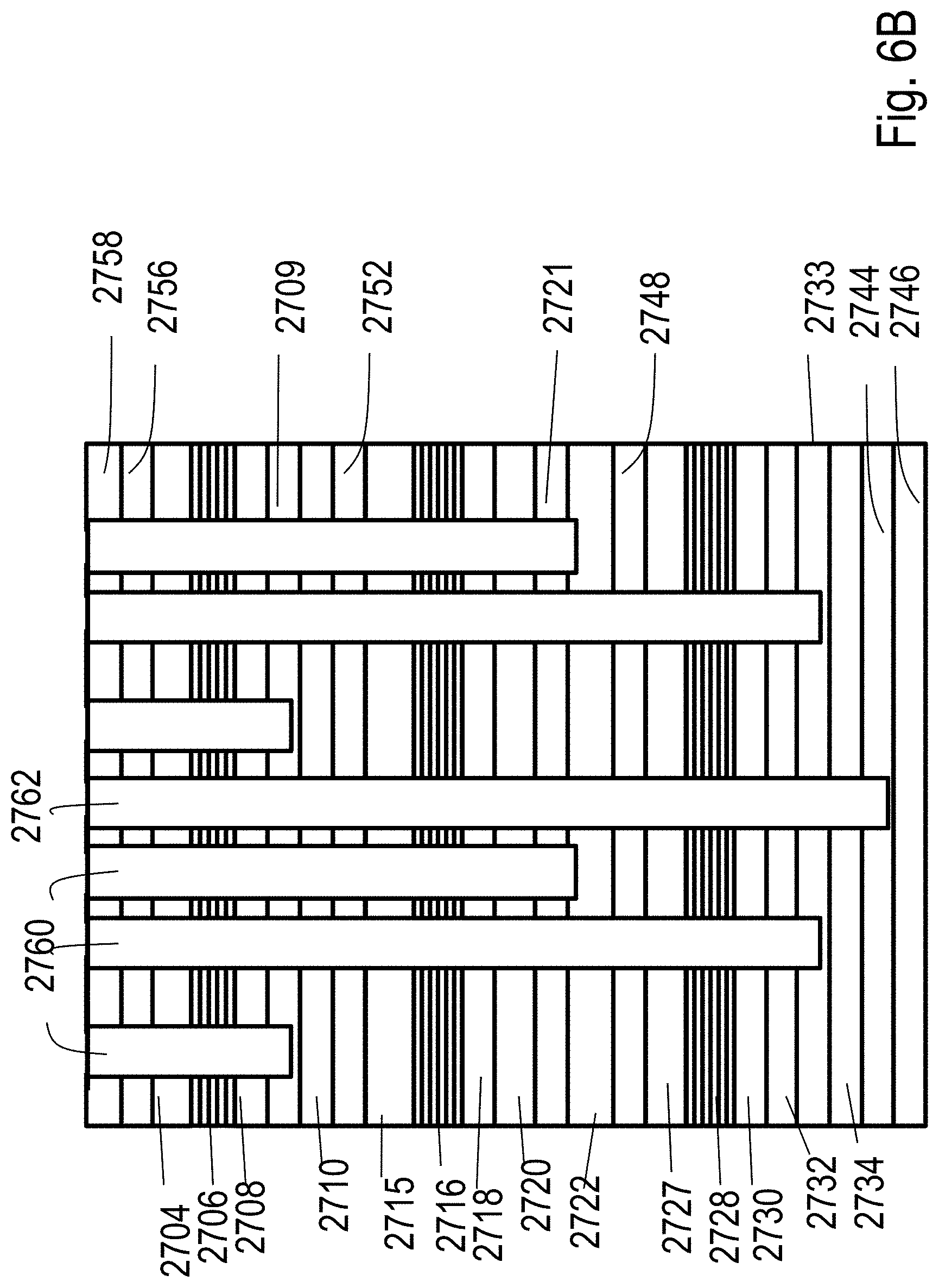
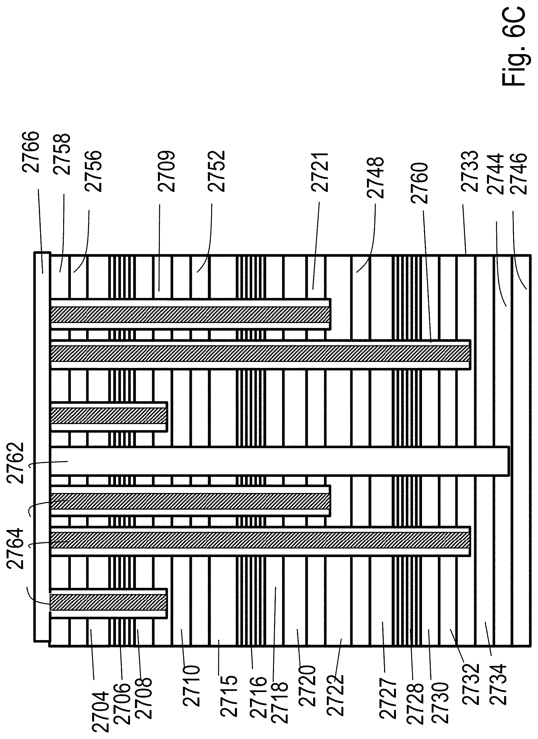
[0049] FIGS. 6A-6D are exemplary drawn illustrations of a microdisplay constructed using stacked RGB LEDs and control circuits are monolithically stacked above the LED.
DETAILED DESCRIPTION
[0050] Embodiments of the present invention are now described with reference to FIGS. 1-6, it being appreciated that the figures illustrate the subject matter not to scale or to measure.
[0051] A smart layer transfer may be defined as one or more of the following processes: [0052] Ion-cut, variations of which are referred to as smart-cut, nano-cleave and smart-cleave: Further information on ion-cut technology is given in "Frontiers of silicon-on-insulator," J. Appl. Phys. 93, 4955-4978 (2003) by G. K. Celler and S. Cristolovean ("Celler") and also in "Mechanically induced Si layer transfer in hydrogen-implanted Si wafers," Appl. Phys. Lett., vol. 76, pp. 2370-2372, 2000 by K. Henttinen, I. Suni, and S. S. Lau ("Hentinnen"). [0053] Porous silicon approaches such as ELTRAN: These are described in "Eltran, Novel SOI Wafer Technology," JSAP International, Number 4, July 2001 by T. Yonehara and K. Sakaguchi ("Yonehara"). [0054] Bonding a substrate with single crystal layers followed by Polishing, Time-controlled etch-back or Etch-stop layer controlled etch-back to thin the bonded substrate: These are described in U.S. Pat. No. 6,806,171 by A. Ulyashin and A. Usenko ("Ulyashin") and "Enabling SOI-Based Assembly Technology for Three-Dimensional (3D) Integrated Circuits (ICs)," IEDM Tech. Digest, p. 363 (2005) by A. W. Topol, D. C. La Tulipe, L. Shi, S. M. Alam, D. J. Frank, S. E. Steen, J. Vichiconti, D. Posillico, M. Cobb, S. Medd, J. Patel, S. Goma, D. DiMilia, M. T. Robson, E. Duch, M. Farinelli, C. Wang, R. A. Conti, D. M. Canaperi, L. Deligianni, A. Kumar, K. T. Kwietniak, C. D'Emic, J. Ott, A. M. Young, K. W. Guarini, and M. Ieong ("Topol"). [0055] Bonding a wafer with a Gallium Nitride film epitaxially grown on a sapphire substrate followed by laser lift-off for removing the transparent sapphire substrate: This method may be suitable for deposition of Gallium Nitride thin films, and is described in U.S. Pat. No. 6,071,795 by Nathan W. Cheung, Timothy D. Sands and William S. Wong ("Cheung"). [0056] Rubber stamp layer transfer: This is described in "Solar cells sliced and diced," 19 May 2010, Nature News.
[0057] This process of constructing RGB LEDs could include several steps that occur in a sequence from Step (A) to Step (S). Many of them share common characteristics, features, modes of operation, etc. When the same reference numbers are used in different drawing figures, they are used to indicate analogous, similar or identical structures to enhance the understanding of the present invention by clarifying the relationships between the structures and embodiments presented in the various diagrams--particularly in relating analogous, similar or identical functionality to different physical structures.
NuDisplay Technology:
[0058] In displays and microdisplays (small size displays where optical magnification is needed), transistors need to be formed on glass or plastic substrates. These substrates typically cannot withstand high process temperatures (e.g., >400.degree. C.). Layer transfer can be advantageously used for constructing displays and microdisplays as well, since it may enable transistors to be processed on these substrates at <400.degree. C. Various embodiments of transistors constructed on glass substrates are described in this patent application. These transistors constructed on glass substrates could form part of liquid crystal displays (LCDs) or other types of displays. It will be clear to those skilled in the art based on the present disclosure that these techniques can also be applied to plastic substrates.
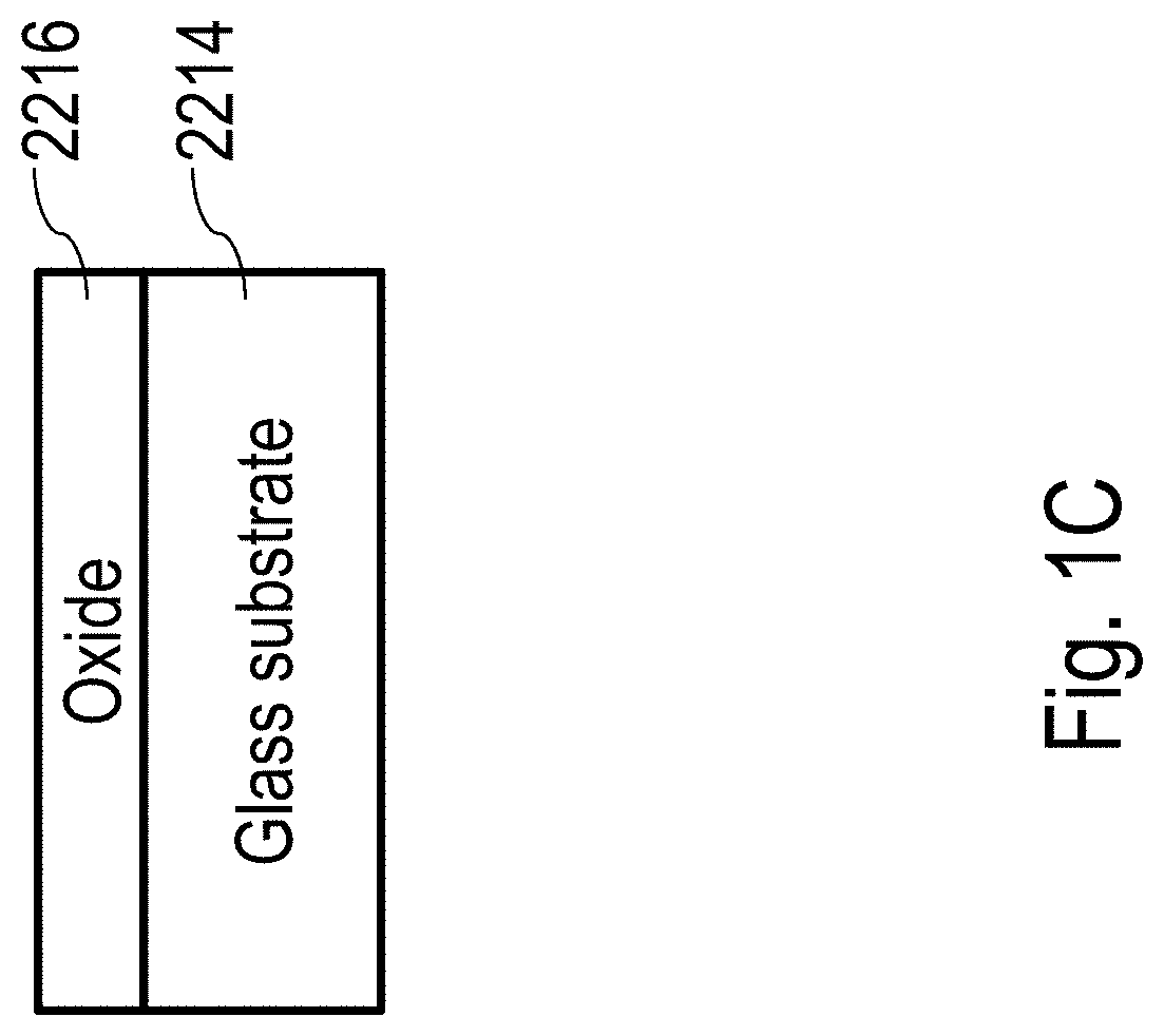
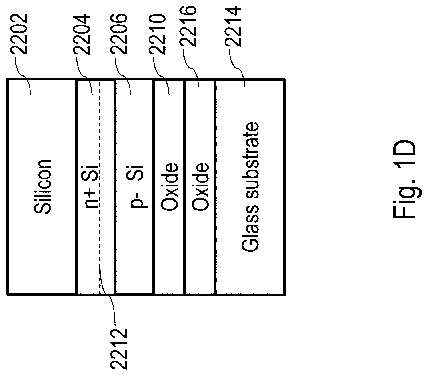
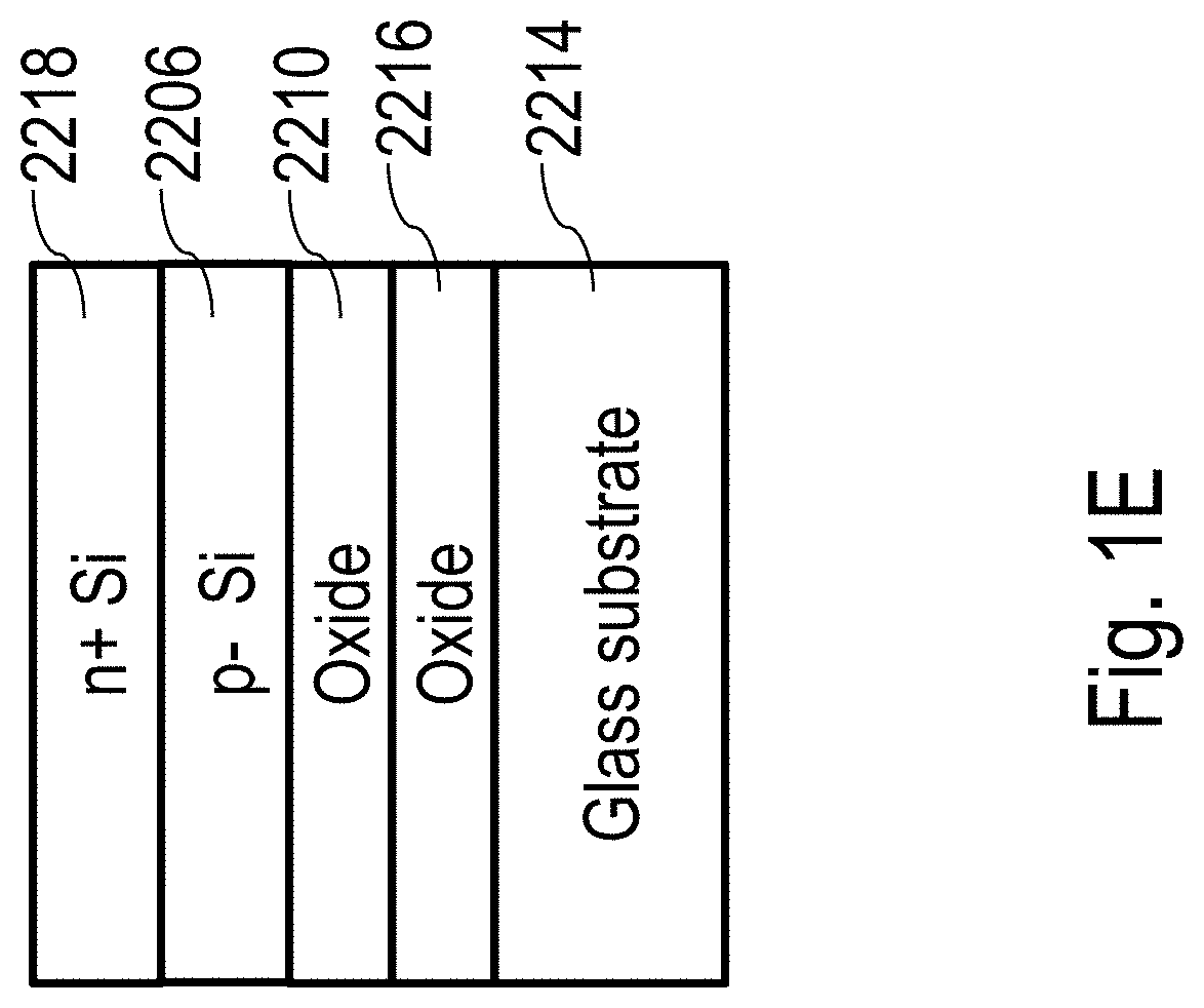
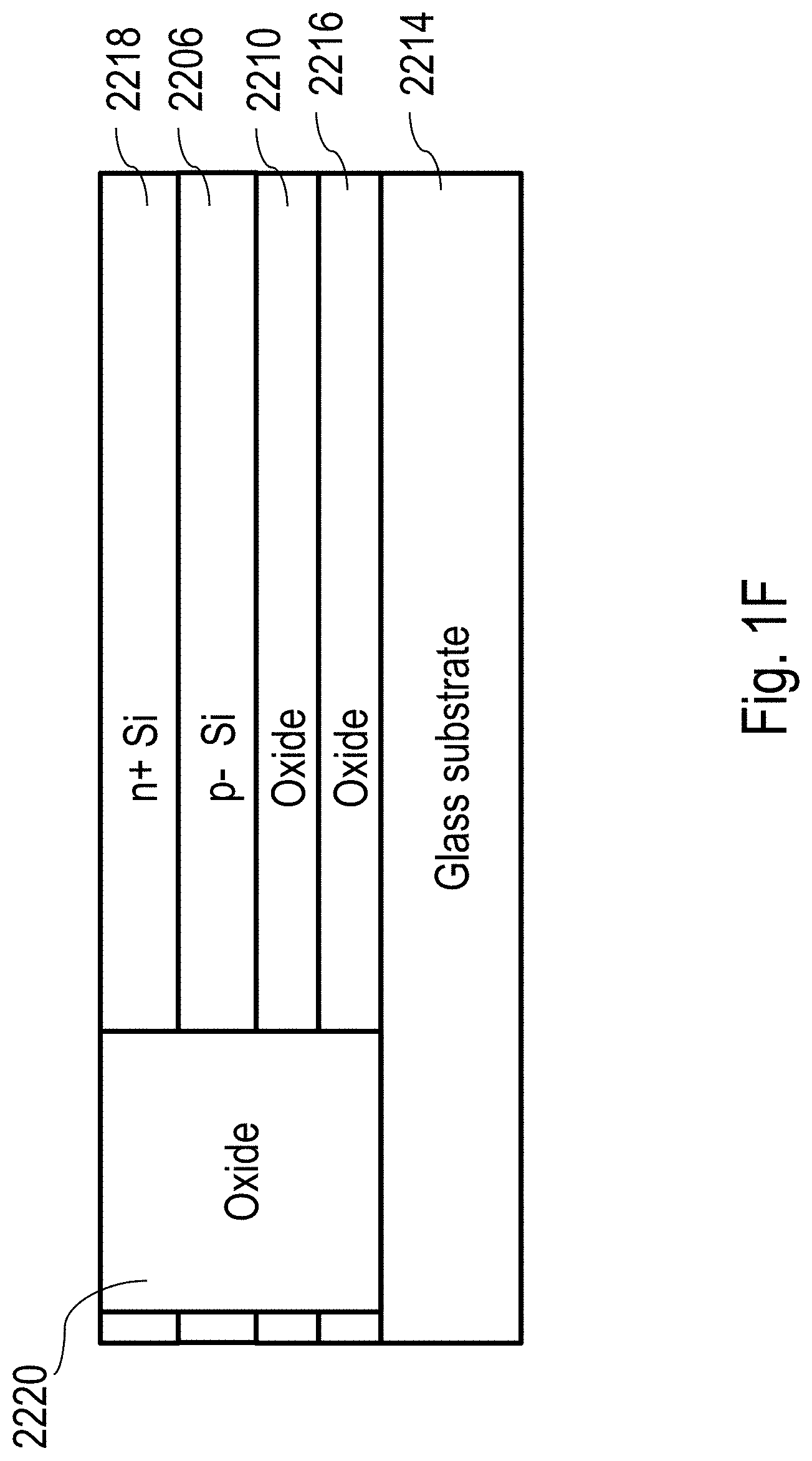
[0059] FIGS. 1A-1G describe a process for forming recessed channel single crystal (or monocrystalline) transistors on glass substrates at a temperature approximately less than 400.degree. C. for display and microdisplay applications. This process could include several steps that occur in a sequence from Step (A) to Step (G). Many of these steps share common characteristics, features, modes of operation, etc. When identical reference numbers are used in different drawing figures, they are used to indicate analogous, similar or identical structures to enhance the understanding of the present invention by clarifying the relationships between the structures and embodiments presented in the various diagrams--particularly in relating analogous, similar or identical functionality to different physical structures. [0060] Step (A) is illustrated in FIG. 1A. A silicon wafer 2202 is taken and a n+ region 2204 is formed by ion implantation. Following this formation, a layer of p- Silicon 2206 is epitaxially grown. An oxide layer 2210 is then deposited. Following this deposition, an anneal is performed to activate dopants in various layers. It will be clear to one skilled in the art based on the present disclosure that various other procedures can be used to get the structure shown in FIG. 22A. [0061] Step (B) is illustrated in FIG. 1B. Hydrogen is implanted into the structure shown in FIG. 22A at a certain depth indicated by 2212. Alternatively, Helium can be used for this purpose. Various elements in FIG. 1B, such as 2202, 2204, 2006, and 2210 have been described previously. [0062] Step (C) is illustrated in FIG. 1C. A glass substrate 2214 is taken and a silicon oxide layer 2216 is deposited atop it at compatible temperatures. [0063] Step (D) is illustrated in FIG. 1D. Various elements in FIG. 1D, such as 2202, 2204, 2206, 2210, 2214, and 2216 have been described previously. The structure shown in FIG. 1B is flipped and bonded to the structure shown in FIG. 1C using oxide-to-oxide bonding of layers 2210 and 2216. [0064] Step (E) is illustrated in FIG. 1E. The structure shown in FIG. 1D is cleaved at the hydrogen plane 2212 of FIG. 1D. A CMP is then done to planarize the surface and yield the n+ Si layer 2218. Various other elements in FIG. 1E, such as 2214, 2216, 2210 and 2206 have been described previously. [0065] Step (F) is illustrated in FIG. 1F. Various elements in FIG. 1F such as 2214, 2216, 2210, and 2206 have been described previously. An oxide layer 2220 is formed using a shallow trench isolation (STI) process. This helps isolate transistors. [0066] Step (G) is illustrated in FIG. 1G. Various elements in FIG. 1G such as 2210, 2216, 2220 and 2214 have been described previously. Using etch techniques, part of the n+ Silicon layer from FIG. 1F and optionally p- Silicon layer from FIG. 1F are etched. After this a thin gate dielectric is deposited, after which a gate dielectrode is deposited. The gate dielectric and gate electrode are then polished away to form the gate dielectric layer 2224 and gate electrode layer 2222. The n+ Silicon layers 2228 and 2226 form the source and drain regions of the transistors while the p- Silicon region after this step is indicated by 2230. Contacts and other parts of the display/microdisplay are then fabricated. It can be observed that during the whole process, the glass substrate substantially always experiences temperatures less than 400.degree. C., or even lower. This is because the crystalline silicon can be transferred atop the glass substrate at a temperature less than 400.degree. C., and dopants are pre-activated before layer transfer to glass.
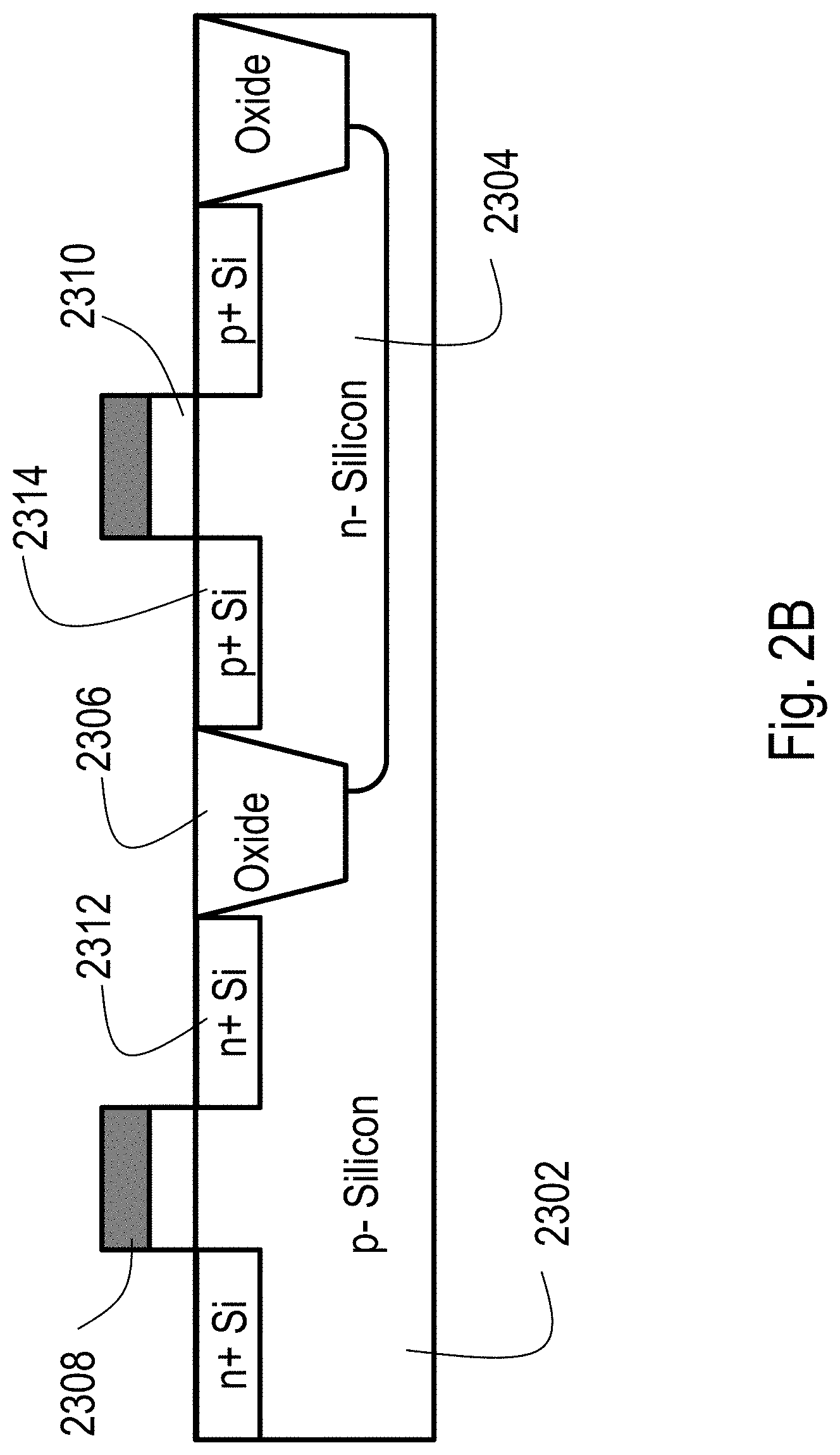
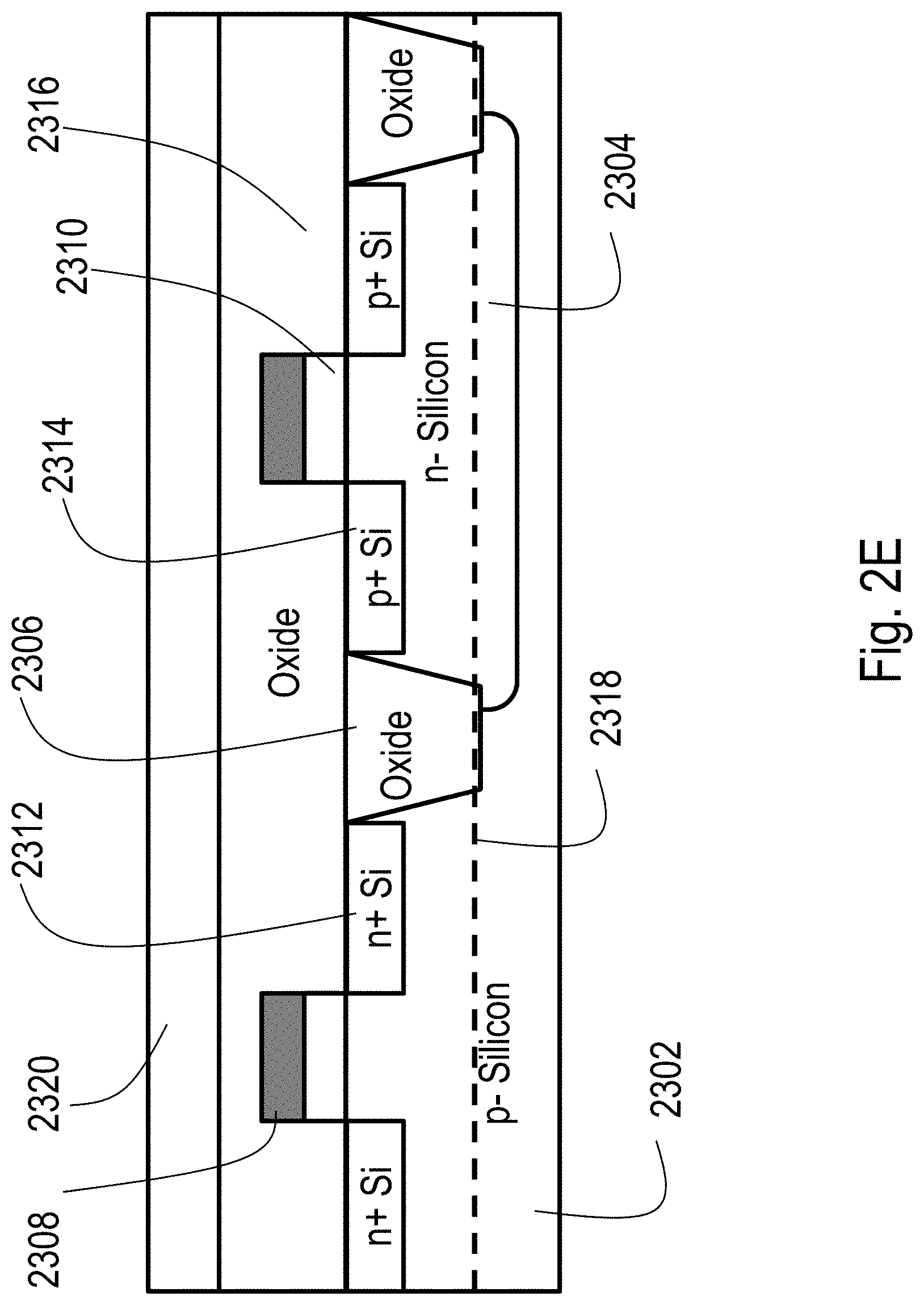
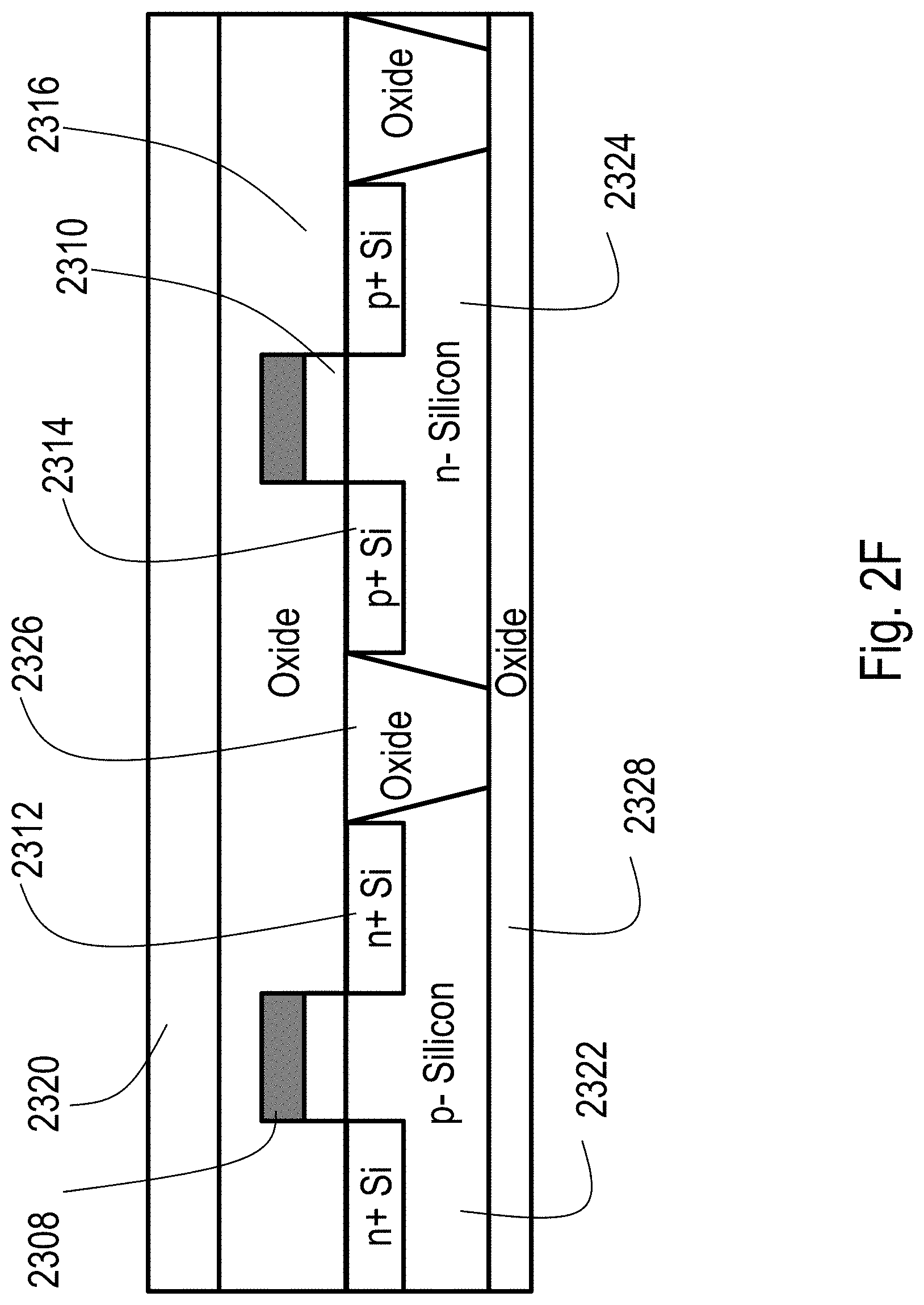
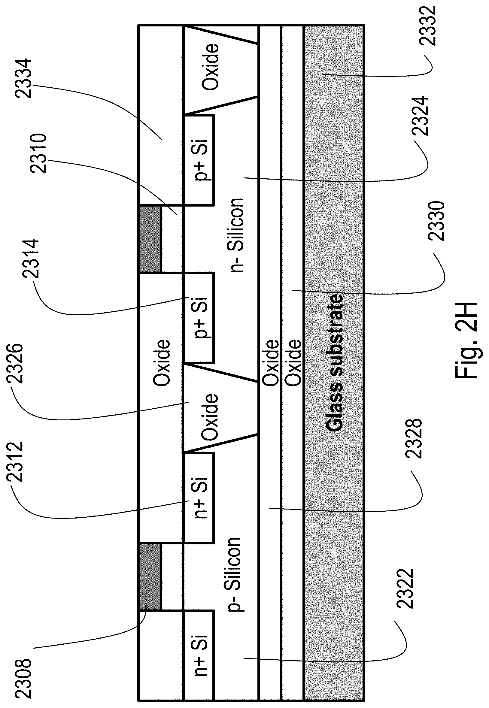
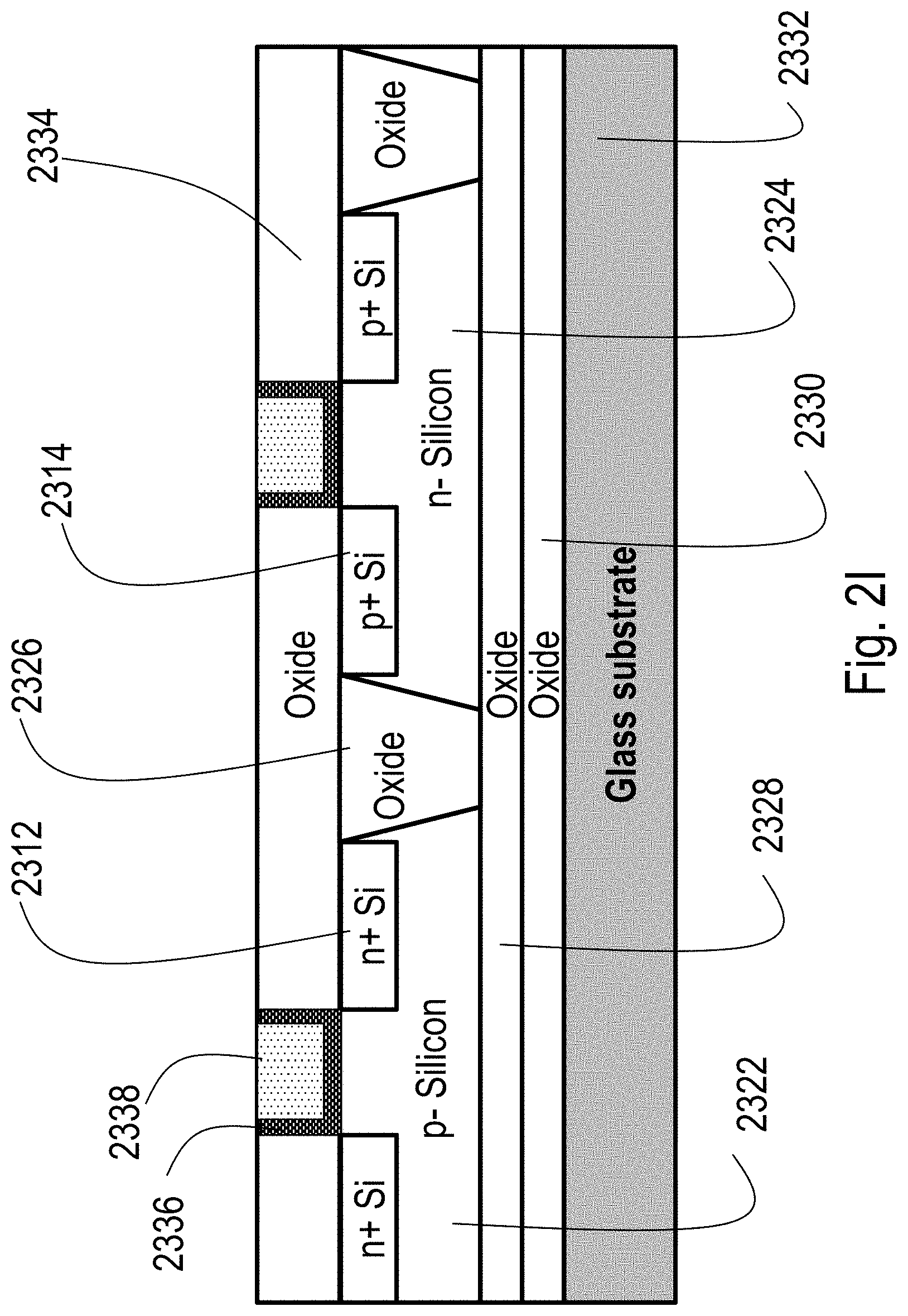
[0067] FIG. 2A-21 describes a process of forming both nMOS and pMOS transistors with single-crystal silicon on a glass substrate at temperatures less than 400.degree. C., and even lower. Ion-cut technology (which is a smart layer transfer technology) is used. While the process flow described is shown for both nMOS and pMOS on a glass substrate, it could also be used for just constructing nMOS devices or for just constructing pMOS devices. This process could include several steps that occur in a sequence from Step (A) to Step (H). Many of these steps share common characteristics, features, modes of operation, etc. When identical reference numbers are used in different drawing figures, they are used to indicate analogous, similar or identical structures to enhance the understanding of the present invention by clarifying the relationships between the structures and embodiments presented in the various diagrams--particularly in relating analogous, similar or identical functionality to different physical structures. [0068] Step (A) is illustrated in FIG. 2A. A p- Silicon wafer 2302 is taken and a n well 2304 is formed on the p- Silicon wafer 2302. Various additional implants to optimize dopant profiles can also be done. Following this formation, an isolation process is conducted to form isolation regions 2306. A dummy gate dielectric 2310 made of silicon dioxide and a dummy gate electrode 2308 made of polysilicon are constructed. [0069] Step (B) is illustrated in FIG. 2B. Various elements of FIG. 2B, such as 2302, 2304, 2306, 2308 and 2310 have been described previously. Implants are done to form source-drain regions 2312 and 2314 for both nMOS and pMOS transistors. A rapid thermal anneal (RTA) is then done to activate dopants. Alternatively, a spike anneal or a laser anneal could be done. [0070] Step (C) is illustrated in FIG. 2C. Various elements of FIG. 2C such as 2302, 2304, 2306, 2308, 2310, 2312 and 2314 have been described previously. An oxide layer 2316 is deposited and planarized with CMP. [0071] Step (D) is illustrated in FIG. 2D. Various elements of FIG. 2D such as 2302, 2304, 2306, 2308, 2310, 2312, 2314, and 2316 have been described previously. Hydrogen is implanted into the wafer at a certain depth indicated by 2318. Alternatively, helium can be implanted. [0072] Step (E) is illustrated in FIG. 2E. Various elements of FIG. 2E such as 2302, 2304, 2306, 2308, 2310, 2312, 2314, 2316, and 2318 have been described previously. Using a temporary bonding adhesive, the oxide layer is bonded to a temporary carrier wafer 2320. An example of a temporary bonding adhesive is a polyimide that can be removed by shining a laser. An example of a temporary carrier wafer is glass. [0073] Step (F) is illustrated in FIG. 2F. The structure shown in FIG. 2E is cleaved at the hydrogen plane using a mechanical force. Alternatively, an anneal could be used. Following this cleave, a CMP is done to planarize the surface. An oxide layer is then deposited. FIG. 2F shows the structure after all these steps are done, with the deposited oxide layer indicated as 2328. After the cleave, the p- Silicon region is indicated as 2322, the n- Silicon region is indicated as 2324, and the oxide isolation regions are indicated as 2326. Various other elements in FIG. 23F such as 2308, 2320, 2312, 2314, 2310, and 2316 have been described previously. [0074] Step (G) is illustrated in FIG. 2G. The structure shown in FIG. 2F is bonded to a glass substrate 2332 with an oxide layer 2330 using oxide-to-oxide bonding. Various elements in FIG. 2G such as 2308, 2326, 2322, 2324, 2312, 2314, and 2310 have been described previously. Oxide regions 2328 and 2330 are bonded together. The temporary carrier wafer from FIG. 2F is removed by shining a laser through it. A CMP process is then conducted to reach the surface of the gate electrode 2308. Thus, the structure may be illustrated by FIG. 2H. The oxide layer remaining is denoted as 2334. Step (H) is illustrated in FIG. 21. Various elements in FIG. 21 such as 2312, 2314, 2328, 2330, 2332, 2334, 2326, 2324, and 2322 have been described previously. The dummy gate dielectric and dummy gate electrode are etched away in this step and a replacement gate dielectric 2336 and a replacement gate electrode 2338 are deposited and planarized with CMP. Examples of replacement gate dielectrics could be hafnium oxide or aluminum oxide while examples of replacement gate electrodes could be TiN or TaN or some other material. Contact formation, metallization and other steps for building a display/microdisplay are then conducted. It can be observed that after attachment to the glass substrate, no process step requires a processing temperature above 400.degree. C.
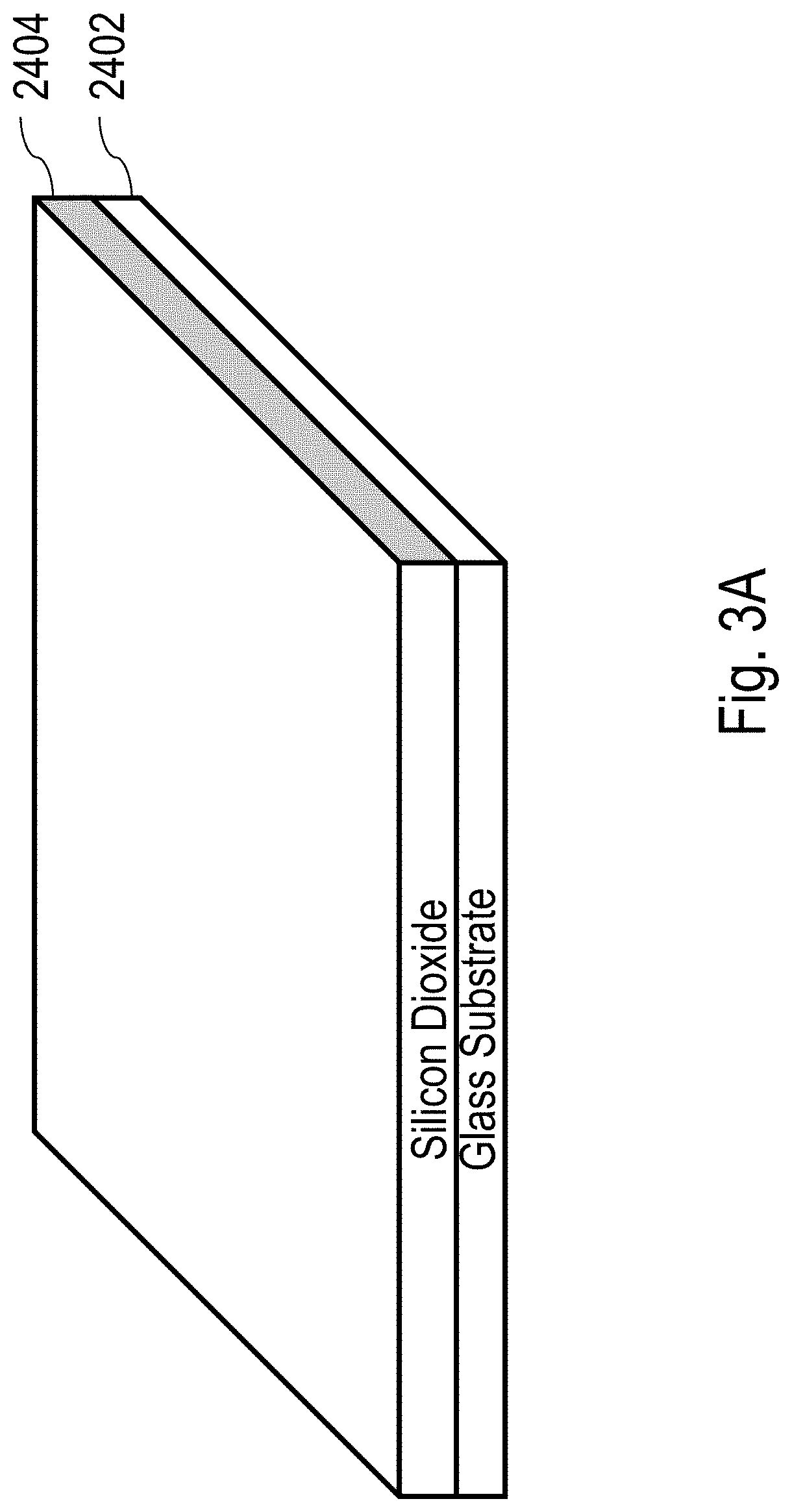
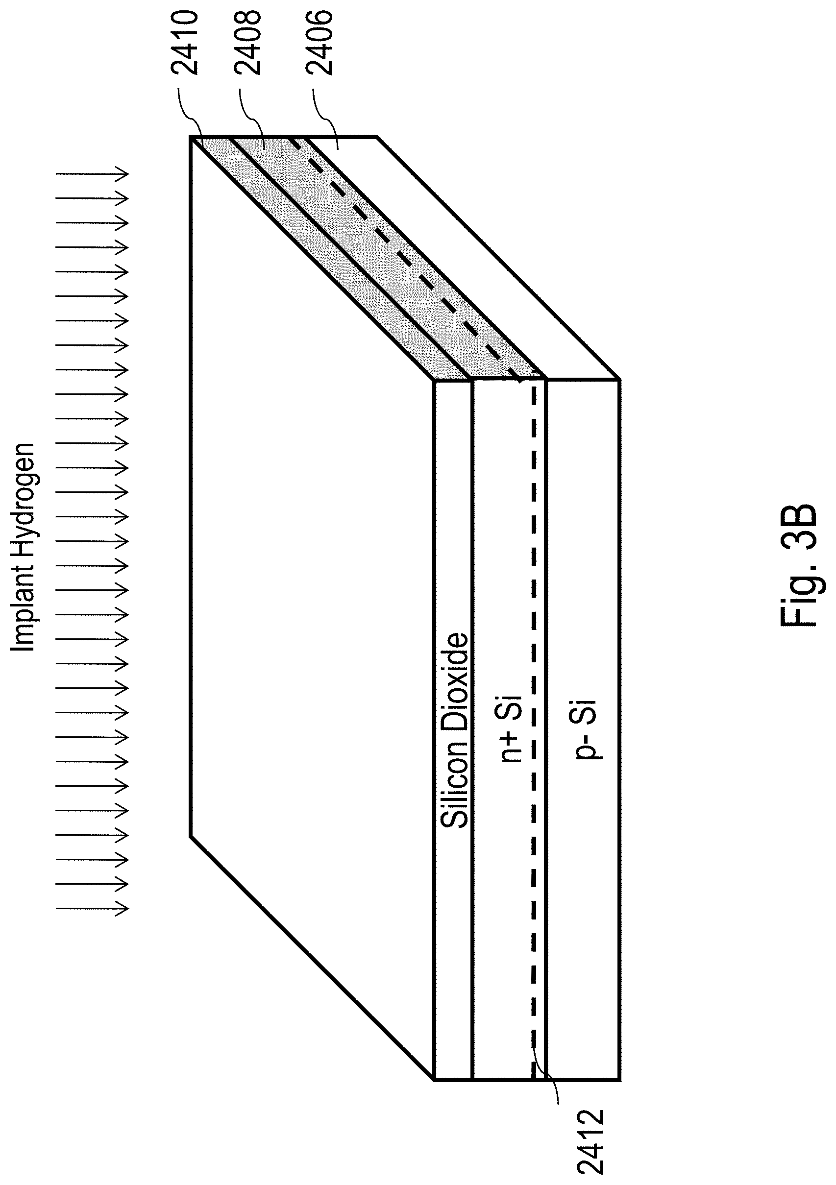
[0075] FIGS. 3A-3F describe an embodiment of this invention, where single-crystal Silicon junction-less transistors are constructed above glass substrates at a temperature approximately less than 400.degree. C. An ion-cut process (which is a smart layer transfer process) is utilized for this purpose. This process could include several steps that occur in a sequence from Step (A) to Step (F). Many of these steps share common characteristics, features, modes of operation, etc. When identical reference numbers are used in different drawing figures, they are used to indicate analogous, similar or identical structures to enhance the understanding of the present invention by clarifying the relationships between the structures and embodiments presented in the various diagrams--particularly in relating analogous, similar or identical functionality to different physical structures. [0076] Step (A) is illustrated in FIG. 3A. A glass substrate 2402 is taken and a layer of silicon oxide 2404 is deposited on the glass substrate 2402. [0077] Step (B) is illustrated in FIG. 3B. A p- Silicon wafer 2406 is implanted with a n+ Silicon layer 2408 above which an oxide layer 2410 is deposited. A RTA or spike anneal or laser anneal is conducted to activate dopants. Following this, hydrogen is implanted into the wafer at a certain depth indicated by 2412. Alternatively, helium can be implanted. [0078] Step (C) is illustrated in FIG. 3C. The structure shown in FIG. 3B is flipped and bonded onto the structure shown in FIG. 3A using oxide-to-oxide bonding. This bonded structure is cleaved at its hydrogen plane, after which a CMP is done. FIG. 3C shows the structure after all these processes are completed. 2414 indicates the n+ Si layer, while 2402, 2404, and 2410 have been described previously. [0079] Step (D) is illustrated in FIG. 3D. A lithography and etch process is conducted to pattern the n+ Silicon layer 2414 in FIG. 3C to form n+ Silicon regions 2418 in FIG. 3D. The glass substrate is indicated as 2402 and the bonded oxide layers 2404 and 2410 are shown as well. [0080] Step (E) is illustrated in FIG. 3E. A gate dielectric 2420 and gate electrode 2422 are deposited, following which a CMP is done. 2402 is as described previously. The n+ Si regions 2418 are not visible in this figure, since they are covered by the gate electrode 2422. Oxide regions 2404 and 2410 have been described previously. [0081] Step (F) is illustrated in FIG. 3F. The gate dielectric 2420 and gate electrode 2422 from FIG. 3E are patterned and etched to form the structure shown in FIG. 3F. The gate dielectric after the etch process is indicated as 2424 while the gate electrode after the etch process is indicated as 2426. n+ Si regions are indicated as 2418 while the glass substrate is indicated as 2402. Oxide regions 2404 and 2410 have been described previously. It can be observed that a three-side gated junction-less transistor is formed at the end of the process described with respect of FIGS. 3A-3F. Contacts, metallization and other steps for constructing a display/microdisplay are performed after the steps indicated by FIGS. 3A-3F. It can be seen that the glass substrate is not exposed to temperatures greater than approximately 400.degree. C. during any step of the above process for forming the junction-less transistor.
[0082] FIGS. 4A-D describe an embodiment of this invention, where amorphous Si or polysilicon junction-less transistors are constructed above glass substrates at a temperature less than 400.degree. C. This process could include several steps that occur in a sequence from Step (A) to Step (D). Many of these steps share common characteristics, features, modes of operation, etc. When identical reference numbers are used in different drawing figures, they are used to indicate analogous, similar or identical structures to enhance the understanding of the present invention by clarifying the relationships between the structures and embodiments presented in the various diagrams--particularly in relating analogous, similar or identical functionality to different physical structures. [0083] Step (A) is illustrated in FIG. 4A. A glass substrate 2502 is taken and a layer of silicon oxide 2504 is deposited on the glass substrate 2502. Following this deposition, a layer of n+ Si 2506 is deposited using low-pressure chemical vapor deposition (LPCVD) or plasma enhanced chemical vapor deposition (PECVD). This layer of n+ Si could optionally be hydrogenated. [0084] Step (B) is illustrated in FIG. 4B. A lithography and etch process is conducted to pattern the n+ Silicon layer 2506 in FIG. 4A to form n+ Silicon regions 2518 in FIG. 4B. 2502 and 2504 have been described previously. [0085] Step (C) is illustrated in FIG. 4C. A gate dielectric 2520 and gate electrode 2522 are deposited, following which a CMP is optionally done. 2502 is as described previously. The n+ Si regions 2518 are not visible in this figure, since they are covered by the gate electrode 2522. [0086] Step (D) is illustrated in FIG. 4D. The gate dielectric 2520 and gate electrode 2522 from FIG. 4C are patterned and etched to form the structure shown in FIG. 4D. The gate dielectric after the etch process is indicated as 2524 while the gate electrode after the etch process is indicated as 2526. n+ Si regions are indicated as 2518 while the glass substrate is indicated as 2502. It can be observed that a three-side gated junction-less transistor is formed at the end of the process described with respect of FIGS. 4A-4D. Contacts, metallization and other steps for constructing a display/microdisplay are performed after the steps indicated by FIGS. 4A-4D. It can be seen that the glass substrate is not exposed to temperatures greater than 400.degree. C. during any step of the above process for forming the junction-less transistor.
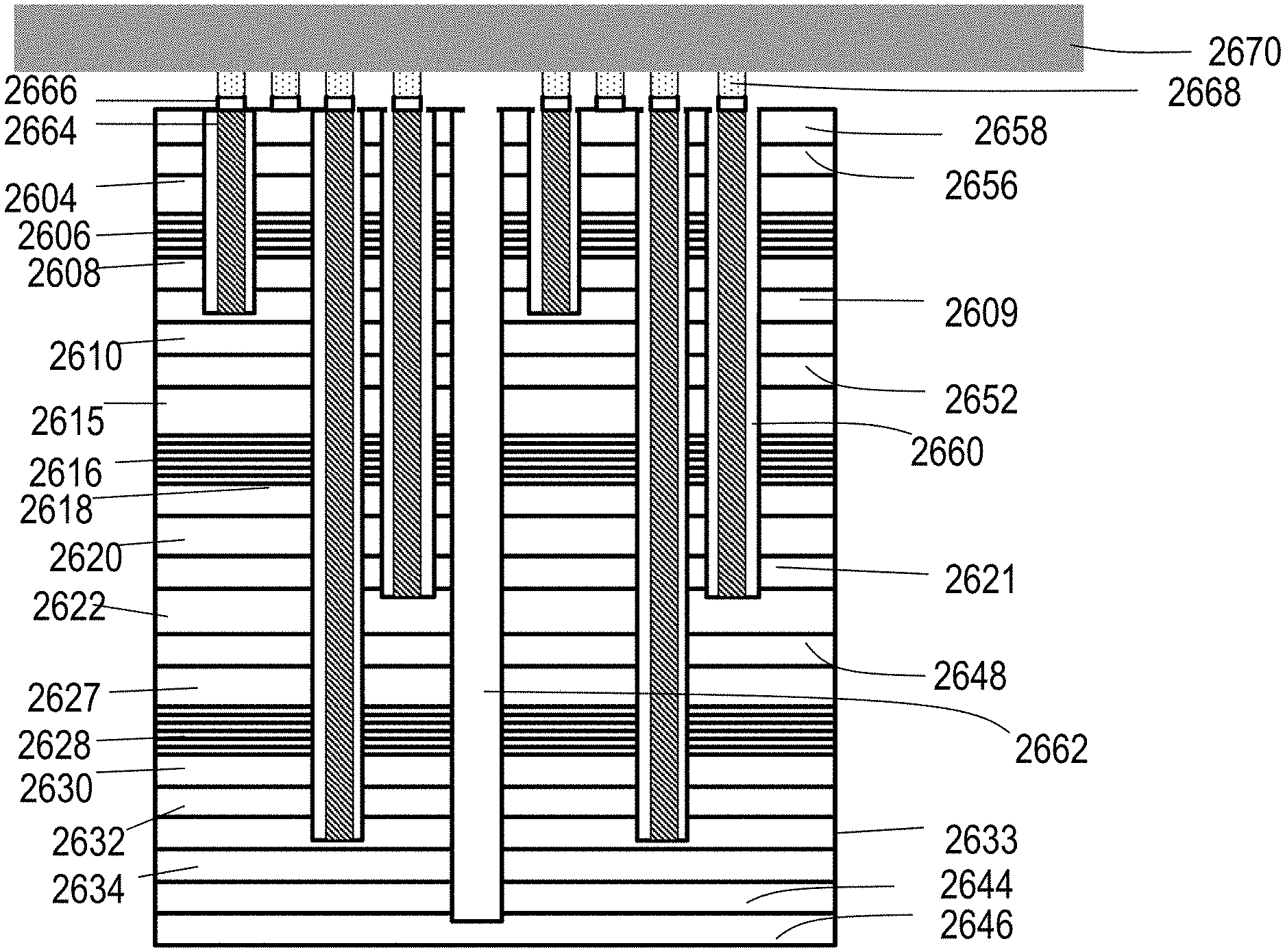
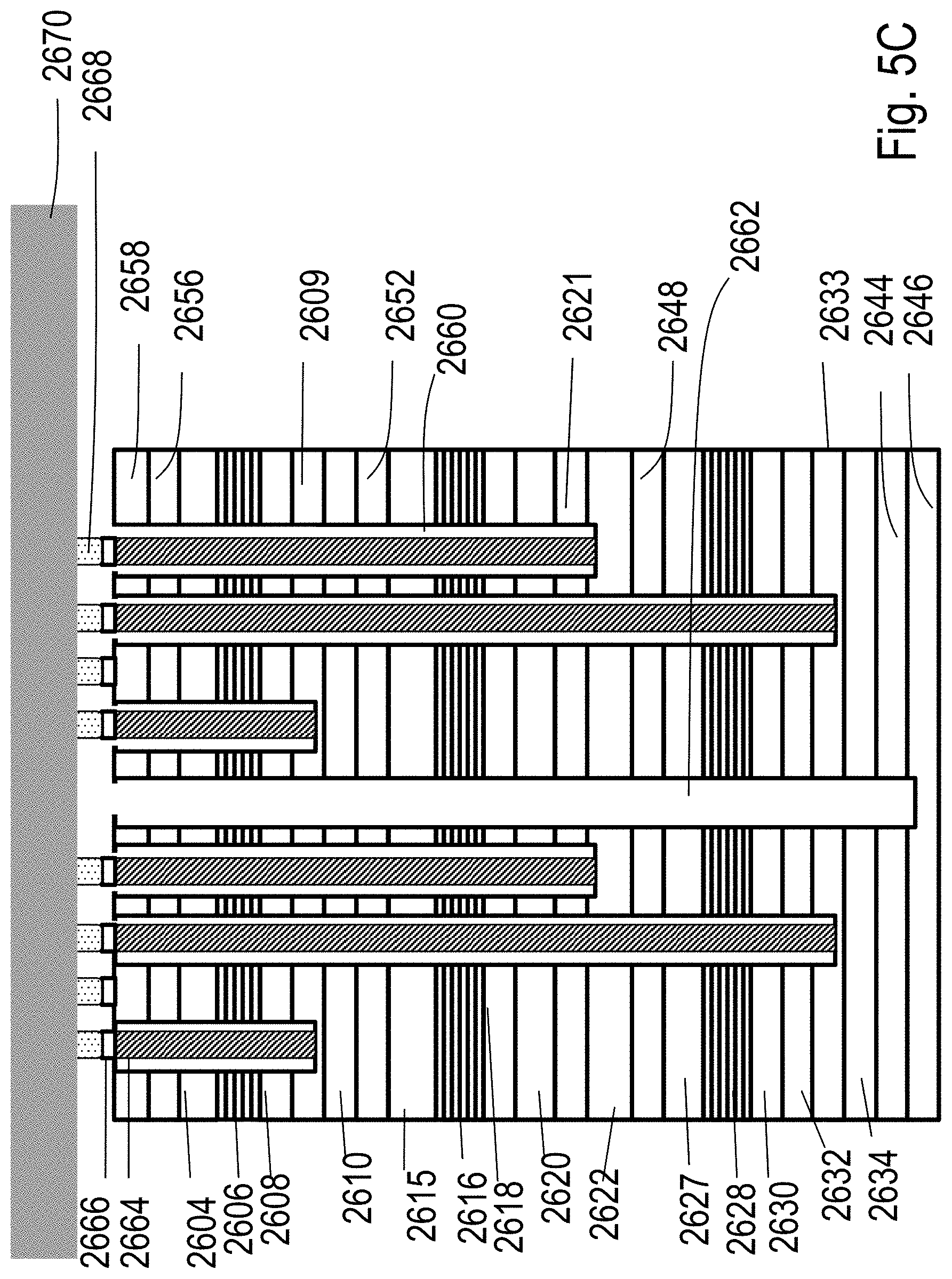
[0087] FIGS. 5A-5C illustrate an embodiment of this invention, where a microdisplay is constructed using stacked RGB LEDs and control circuits are connected to each pixel with solder bumps. This process could include several steps that occur in a sequence from Step (A) to Step (C). Many of these steps share common characteristics, features, modes of operation, etc. When identical reference numbers are used in different drawing figures, they are used to indicate analogous, similar or identical structures to enhance the understanding of the present invention by clarifying the relationships between the structures and embodiments presented in the various diagrams--particularly in relating analogous, similar or identical functionality to different physical structures. [0088] Step (A) is illustrated in FIG. 5A. Using procedures similar to FIG. 4A-4S of parent U.S. patent application Ser. 13/274,161 issued as U.S. Pat. No. 9,197,804, incorporated herein by reference, the structure shown in FIG. 5A is constructed. Various elements of FIG. 5A are as follows: [0089] 2646--a glass substrate, [0090] 2644--an oxide layer, could be a conductive oxide such as ITO, [0091] 2634--an oxide layer, could be a conductive oxide such as ITO [0092] 2633--a an optional reflector, could be a Distributed Bragg Reflector or some other type of reflector, [0093] 2632--a P-type confinement layer that is used for a Blue LED (One example of a material for this region is GaN), [0094] 2630--a buffer layer that is typically used for a Blue LED (One example of a material for this region is AlGaN), [0095] 2628--a multiple quantum well used for a Blue LED (One example of materials for this region are InGaN/GaN), [0096] 2627--a N-type confinement layer that is used for a Blue LED (One example of a material for this region is GaN). [0097] 2648--an oxide layer, may be preferably a conductive metal oxide such as ITO, [0098] 2622--an oxide layer, may be preferably a conductive metal oxide such as ITO, [0099] 2621--an optional reflector (for example, a Distributed Bragg Reflector), [0100] 2620--a P-type confinement layer that is used for a Green LED (One example of a material for this region is GaN), [0101] 2618--a buffer layer that is typically used for a Green LED (One example of a material for this region is AlGaN), [0102] 2616--a multiple quantum well used for a Green LED (One example of materials for this region are InGaN/GaN), [0103] 2615--a N-type confinement layer that is used for a Green LED (One example of a material for this region is GaN), [0104] 2652--an oxide layer, may be preferably a conductive metal oxide such as ITO, [0105] 2610--an oxide layer, may be preferably a conductive metal oxide such as ITO, [0106] 2609--an optional reflector (for example, a Distributed Bragg Reflector), [0107] 2608--a P-type confinement layer used for a Red LED (One example of a material for this region is AlInGaP), [0108] 2606--a multiple quantum well used for a Red LED (One example of materials for this region are AlInGaP/GaInP), [0109] 2604--a P-type confinement layer used for a Red LED (One example of a material for this region is AlInGaP), [0110] 2656--an oxide layer, may be preferably a transparent conductive metal oxide such as ITO, and [0111] 2658--a reflector (for example, aluminum or silver). [0112] Step (B) is illustrated in FIG. 5B. Via holes 2662 are etched to the substrate layer 2646 to isolate different pixels in the microdisplay/display. Also, via holes 2660 are etched to make contacts to various layers of the stack. These via holes may be preferably not filled. An alternative is to fill the via holes with a compatible oxide and planarize the surface with CMP. Various elements in FIG. 5B such as 2646, 2644, 2634, 2633, 2632, 2630, 2628, 2627, 2648, 2622, 2621, 2620, 2618, 2616, 2615, 2652, 2610, 2609, 2608, 2606, 2604, 2656 and 2658 have been described previously. [0113] Step (C) is illustrated in FIG. 5C. Using procedures similar to those described in respect to FIGS. 4A-4S of parent U.S. patent application Ser. No. 13/274,161 issued as U.S. Pat. No. 9,197,804, incorporated herein by reference, the via holes 2660 have contacts 2664 (for example, with Aluminum) made to them. Also, using procedures similar to those described in FIGS. 4A-4S, nickel layers 2666, solder layers 2668, and a silicon sub-mount 2670 with circuits integrated on them are constructed. The silicon sub-mount 2670 has transistors to control each pixel in the microdisplay/display. Various elements in FIG. 5C such as 2646, 2644, 2634, 2633, 2632, 2630, 2628, 2627, 2648, 2622, 2621, 2620, 2618, 2616, 2615, 2652, 2610, 2609, 2608, 2606, 2604, 2656, 2660, 2662, and 2658 have been described previously.
[0114] It can be seen that the structure shown in FIG. 5C can have each pixel emit a certain color of light by tuning the voltage given to the red, green and blue layers within each pixel. This microdisplay may be constructed using the ion-cut technology, a smart layer transfer technique.
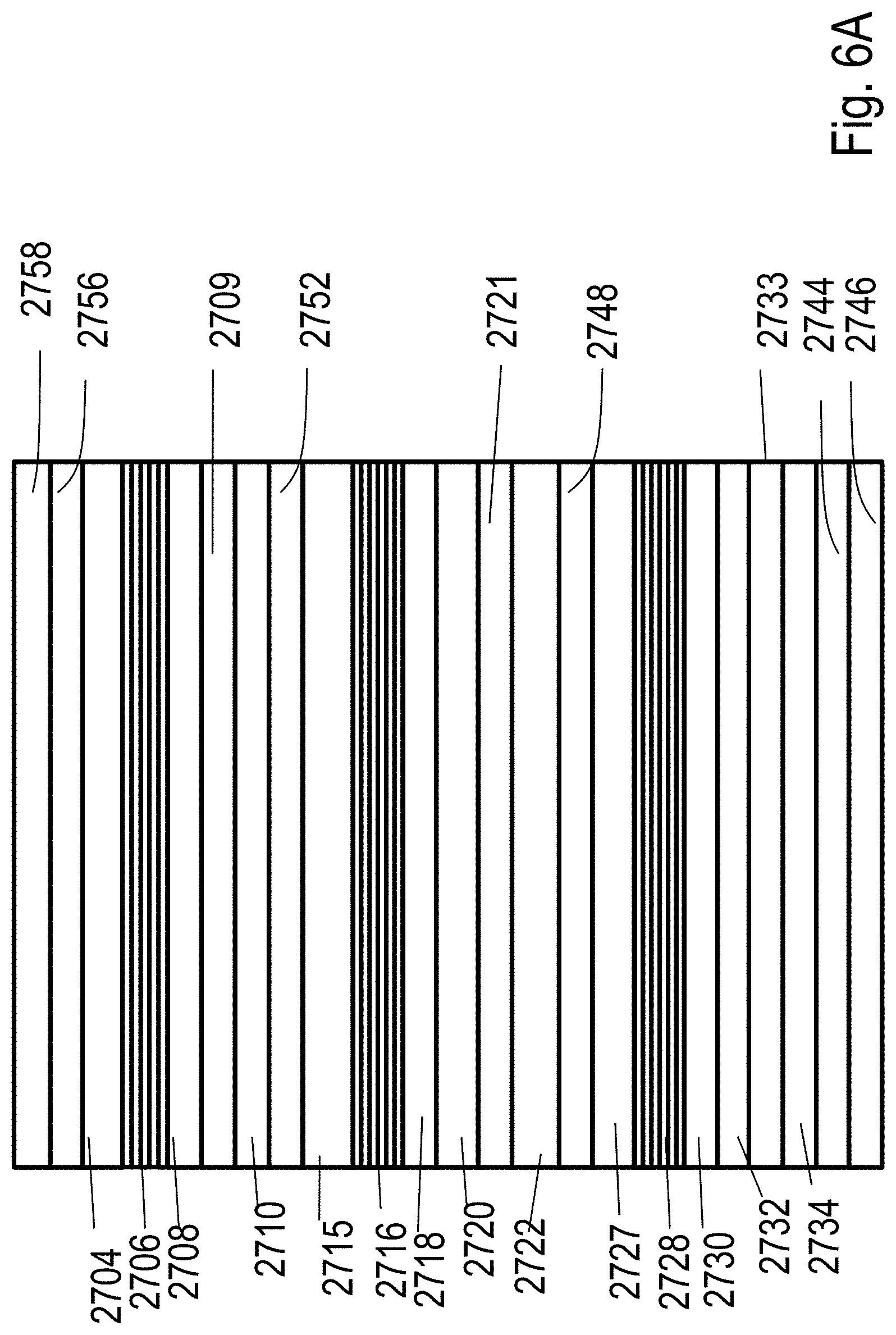
[0115] FIGS. 6A-6D illustrate an embodiment of this invention, where a microdisplay is constructed using stacked RGB LEDs and control circuits are integrated with the RGB LED stack. This process could include several steps that occur in a sequence from Step (A) to Step (D). Many of these steps share common characteristics, features, modes of operation, etc. When identical reference numbers are used in different drawing figures, they are used to indicate analogous, similar or identical structures to enhance the understanding of the present invention by clarifying the relationships between the structures and embodiments presented in the various diagrams--particularly in relating analogous, similar or identical functionality to different physical structures. [0116] Step (A) is illustrated in FIG. 6A. Using procedures similar to those illustrated in FIGS. 4A-4S of parent U.S. patent application Ser. No. 13/274,161 issued as U.S. Pat. No. 9,197,804, incorporated herein by reference, the structure shown in FIG. 6A is constructed. Various elements of FIG. 6A are as follows: [0117] 2746--a glass substrate, [0118] 2744--an oxide layer, could be a conductive oxide such as ITO, [0119] 2734--an oxide layer, could be a conductive oxide such as ITO, [0120] 2733--a an optional reflector (e.g., a Distributed Bragg Reflector or some other type of reflector), [0121] 2732--a P-type confinement layer that is used for a Blue LED (One example of a material for this region is GaN), [0122] 2730--a buffer layer that is typically used for a Blue LED (One example of a material for this region is AlGaN), [0123] 2728--a multiple quantum well used for a Blue LED (One example of materials for this region are InGaN/GaN), [0124] 2727--a N-type confinement layer that is used for a Blue LED (One example of a material for this region is GaN), [0125] 2748--an oxide layer, may be preferably a conductive metal oxide such as ITO, [0126] 2722--an oxide layer, may be preferably a conductive metal oxide such as ITO, [0127] 2721--an optional reflector (e.g., a Distributed Bragg Reflector), [0128] 2720--a P-type confinement layer that is used for a Green LED (One example of a material for this region is GaN), [0129] 2718--a buffer layer that is typically used for a Green LED (One example of a material for this region is AlGaN), [0130] 2716--a multiple quantum well used for a Green LED (One example of materials for this region are InGaN/GaN), [0131] 2715--a N-type confinement layer that is used for a Green LED (One example of a material for this region is GaN), [0132] 2752--an oxide layer, may be preferably a conductive metal oxide such as ITO, [0133] 2710--an oxide layer, may be preferably a conductive metal oxide such as ITO, [0134] 2709--an optional reflector (e.g., a Distributed Bragg Reflector), [0135] 2708--a P-type confinement layer used for a Red LED (One example of a material for this region is AlInGaP), [0136] 2706--a multiple quantum well used for a Red LED (One example of materials for this region are AlInGaP/GaInP), [0137] 2704--a P-type confinement layer used for a Red LED (One example of a material for this region is AlInGaP), [0138] 2756--an oxide layer, may be preferably a transparent conductive metal oxide such as ITO, [0139] 2758--a reflector (e.g., aluminum or silver). [0140] Step (B) is illustrated in FIG. 6B. Via holes 2762 are etched to the substrate layer 2746 to isolate different pixels in the microdisplay/display. Also, via holes 2760 are etched to make contacts to various layers of the stack. These via holes may be preferably filled with a compatible oxide and the surface can be planarized with CMP. Various elements of FIG. 6B such as 2746, 2744, 2734, 2733, 2732, 2730, 2728, 2727, 2748, 2722, 2721, 2720, 2718, 2716, 2715, 2752, 2710, 2709, 2708, 2706, 2704, 2756 and 2758 have been described previously. [0141] Step (C) is illustrated in FIG. 6C. Metal 2764 (for example) is constructed within the via holes 2760 using procedures similar to those described in respect to FIGS. 4A-4S of parent U.S. patent application Ser. No. 13/274,161 issued as U.S. Pat. No. 9,197,804, incorporated herein by reference. Following this construction, an oxide layer 2766 is deposited. Various elements of FIG. 6C such as 2746, 2744, 2734, 2733, 2732, 2730, 2728, 2727, 2748, 2722, 2721, 2720, 2718, 2716, 2715, 2752, 2710, 2709, 2708, 2706, 2704, 2756, 2760, 2762 and 2758 have been described previously. [0142] Step (D) is illustrated in FIG. 6D. Using procedures described in co-pending U.S. patent application Ser. No. 12/901,890, issued as U.S. Pat. No. 8,026,521, the entire contents of which is incorporated herein by reference, a single crystal silicon transistor layer 2768 can be monolithically integrated using ion-cut technology atop the structure shown in FIG. 6C. This transistor layer 2768 is connected to various contacts of the stacked LED layers (not shown in the figure for simplicity). Following this connection, nickel layer 2770 is constructed and solder layer 2772 is constructed. The packaging process then is conducted where the structure shown in FIG. 6D is connected to a silicon sub-mount. It can be seen that the structure shown in FIG. 6D can have each pixel emit a certain color of light by tuning the voltage given to the red, green and blue layers within each pixel. This microdisplay is constructed using the ion-cut technology, a smart layer transfer technique.
[0143] The embodiments of this invention described in FIGS. 5-6 may enable novel implementations of "smart-lighting concepts" (also known as visible light communications) that are described in "Switching LEDs on and off to enlighten wireless communications", EETimes, June 2010 by R. Colin Johnson. For these prior art smart lighting concepts, LED lights could be turned on and off faster than the eye can react, so signaling or communication of information with these LED lights is possible. An embodiment of this invention involves designing the displays/microdisplays described in FIGS. 5-6 to transmit information, by modulating wavelength of each pixel and frequency of switching each pixel on or off. One could thus transmit a high bandwidth through the visible light communication link compared to a LED, since each pixel could emit its own information stream, compared to just one information stream for a standard LED. The stacked RGB LED embodiment described in FIGS. 4A-4S of parent U.S. patent application Ser. No. 13/274,161 issued as U.S. Pat. No. 9,197,804, incorporated herein by reference, could also provide an improved smart-light than prior art since it allows wavelength tunability besides the ability to turn the LED on and off faster than the eye can react.
[0144] Several material systems have been illustrated as examples for various embodiments of this invention in this patent application. It will be clear to one skilled in the art based on the present disclosure that various other material systems and configurations can also be used without violating the concepts described. It will also be appreciated by persons of ordinary skill in the art that the present invention is not limited to what has been particularly shown and described hereinabove. Rather, the scope of the invention includes both combinations and sub-combinations of the various features described herein above as well as modifications and variations which would occur to such skilled persons upon reading the foregoing description. Thus the invention is to be limited only by the appended claims.
* * * * *
D00000
D00001
D00002
D00003
D00004
D00005
D00006
D00007
D00008
D00009
D00010
D00011
D00012
D00013
D00014

D00015
D00016
D00017
D00018
D00019
D00020
D00021
D00022

D00023
D00024
D00025

D00026
D00027

D00028

D00029
D00030
D00031
D00032
D00033

XML
uspto.report is an independent third-party trademark research tool that is not affiliated, endorsed, or sponsored by the United States Patent and Trademark Office (USPTO) or any other governmental organization. The information provided by uspto.report is based on publicly available data at the time of writing and is intended for informational purposes only.
While we strive to provide accurate and up-to-date information, we do not guarantee the accuracy, completeness, reliability, or suitability of the information displayed on this site. The use of this site is at your own risk. Any reliance you place on such information is therefore strictly at your own risk.
All official trademark data, including owner information, should be verified by visiting the official USPTO website at www.uspto.gov. This site is not intended to replace professional legal advice and should not be used as a substitute for consulting with a legal professional who is knowledgeable about trademark law.