Microchip
Kind Code
U.S. patent application number 16/758362 was filed with the patent office on 2020-08-13 for microchip. This patent application is currently assigned to Ushio Denki Kabushiki Kaisha. The applicant listed for this patent is Ushio Denki Kabushiki Kaisha. Invention is credited to Kenji HATAKEYAMA, Kenichi HIROSE, Shinji SUZUKI, Makoto YAMANAKA.
| Application Number | 20200255288 16/758362 |
| Document ID | 20200255288 / US20200255288 |
| Family ID | 1000004825325 |
| Filed Date | 2020-08-13 |
| Patent Application | download [pdf] |
| United States Patent Application | 20200255288 |
| Kind Code | A1 |
| HIROSE; Kenichi ; et al. | August 13, 2020 |
MICROCHIP
Abstract
Provided is a microchip that can achieve a favorable bonding state in the bonding portion between first and second substrates even if the microchip is large in size. A microchip includes a first substrate made of a resin and a second substrate made of a resin, the first substrate and the second substrates being bonded to each other, and a channel surrounded by a bonding portion between the first substrate and the second substrate is formed by a channel forming step formed at least in the first substrate. Further, a noncontact portion is formed to surround the bonding portion, and an angle 01 formed between a side wall surface of the channel forming step and a bonding surface continuous therewith satisfies .theta..sub.1>90.degree..
| Inventors: | HIROSE; Kenichi; (Tokyo, JP) ; YAMANAKA; Makoto; (Tokyo, JP) ; SUZUKI; Shinji; (Tokyo, JP) ; HATAKEYAMA; Kenji; (Tokyo, JP) | ||||||||||
| Applicant: |
|
||||||||||
|---|---|---|---|---|---|---|---|---|---|---|---|
| Assignee: | Ushio Denki Kabushiki
Kaisha Tokyo JP |
||||||||||
| Family ID: | 1000004825325 | ||||||||||
| Appl. No.: | 16/758362 | ||||||||||
| Filed: | August 7, 2018 | ||||||||||
| PCT Filed: | August 7, 2018 | ||||||||||
| PCT NO: | PCT/JP2018/029538 | ||||||||||
| 371 Date: | April 22, 2020 |
| Current U.S. Class: | 1/1 |
| Current CPC Class: | B81C 1/00071 20130101; B81C 2201/019 20130101; B81C 3/001 20130101 |
| International Class: | B81C 3/00 20060101 B81C003/00; B81C 1/00 20060101 B81C001/00 |
Foreign Application Data
| Date | Code | Application Number |
|---|---|---|
| Oct 27, 2017 | JP | 2017-207839 |
Claims
1. A microchip comprising a first substrate made of a resin and a second substrate made of a resin, the first substrate and the second substrates being bonded to each other, a channel surrounded by a bonding portion between the first substrate and the second substrate being formed by a channel forming step formed at least in the first substrate, wherein: a noncontact portion is formed to surround the bonding portion; an angle .theta..sub.1 formed between a side wall surface of the channel forming step and a bonding surface continuous therewith satisfies .theta..sub.1>90.degree.; a bonding surface and the front surface of the second substrate on the side being in contact with the first substrate is configured as a flat surface; and the bonding surface has a width of not less than 500 .mu.m.
2. The microchip according to claim 1, wherein an angle .theta..sub.2 formed between a side wall surface of the noncontact portion and a bonding surface continuous therewith satisfies .theta..sub.2>90.degree..
3. A microchip comprising a first substrate made of a resin and a second substrate made of a resin, the first substrate and the second substrate being bonded to each other, a channel surrounded by a bonding portion between the first substrate and the second substrate being formed by a channel forming step formed at least in the first substrate, wherein: a noncontact portion is formed to surround the bonding portion; at least either a side wall surface of the channel forming step or a side wall surface of the noncontact portion is chamfered or rounded in an area near a bonding surface continuous with the side wall surface; a bonding surface and the front surface of the second substrate on the side being in contact with the first substrate is configured as a flat surface; and the bonding surface has a width of not less than 500 .mu.m.
4. The microchip according to claim 1, wherein a bonding portion between the first substrate and the second substrate is formed at least on part of a periphery of the first substrate and the second substrate.
Description
TECHNICAL FIELD
[0001] The present invention relates to a microchip formed by bonding a first substrate and a second substrate each made of a resin.
BACKGROUND ART
[0002] In the field of biochemistry, techniques for separating, synthesizing, extracting, or analyzing a small amount of reagent by using a microreactor have been attracting attention in recent years. The microreactor includes, for example, a microchip that is a small substrate made of silicon, a silicone resin, glass, or the like on which microscale analysis channels and the like are formed by semiconductor microfabrication techniques.
[0003] A reaction analysis system using such a microreactor is referred to as a micro total analysis system (hereinafter, referred to as a ".mu.TAS"). According to this .mu.TAS, high-speed high-precision reaction analysis can be performed since the ratio of the surface area to volume of the reagent increases. In addition, a compact automated system can be constructed.
[0004] Microchips suited for various applications can be fabricated by providing functional regions having various functions, such as a reaction region where a reagent is located, in channels called microchannels. Examples of the applications of the microchips include analyses in chemical, biochemical, pharmaceutical, medical and veterinary fields, such as genetic analysis, clinical diagnosis and drug screening, synthesis of chemical compounds and environmental measurement.
[0005] Such microchips typically have a structure that a pair of substrates are opposed and bonded to each other. Fine channels, for example, having a width of about 10 to several hundreds of micrometers and a depth of about 10 to several hundreds of micrometers are then formed in the front surface of at least either one of the substrates. For the substrates, glass substrates are mainly used because of easy fabrication and optical detection capabilities. Microchips made of resin substrates that are light-weighted, less breakable and inexpensive compared to glass substrates have been under development recently.
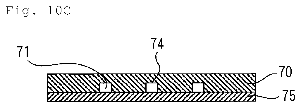
[0006] FIG. 10A is a plan view illustrating a configuration according to an example of a conventional microchip. FIG. 10B is a cross-sectional end view taken along line A-A of FIG. 10A. FIG. 10C is a cross-sectional end view taken along line B-B of FIG. 10A. This microchip includes a first substrate 70 having injection ports 72 into which samples are injected and discharge ports 73 from which the samples are discharged, and a second substrate 75. Channel forming steps 74 for forming channels 71 connecting the injection ports 72 to the discharge ports 73 are formed in the front surface of the first substrate 70. On the other hand, the second substrate 75 is a plate-shaped one having a flat front surface.
[0007] The first substrate 70 and the second substrate 75 are then bonded with their front surfaces in close contact with each other, whereby a microchip including the channels 71 surrounded by the bonding portion between the first substrate 70 and the second substrate 75 is obtained.
[0008] As a method for bonding the first substrate and the second substrate in manufacturing such a microchip, there have been proposed methods including performing an activation treatment on the front surfaces of the respective first and second substrates 70 and 75 to be bonding surfaces, and then stacking the first substrate 70 and the second substrate 75 with their front surfaces in close contact with each other (for example, see Patent Literatures 1 to 5).
[0009] In such microchip manufacturing methods, a vacuum ultraviolet irradiation treatment of irradiating the front surfaces with vacuum ultraviolet rays or a plasma treatment of bringing the front surfaces into contact with atmospheric pressure plasma can be used as the activation treatment on the front surfaces of the respective first and second substrates 70 and 75.
[0010] After the first substrate 70 and the second substrate 75 are stacked, either one or both of a heating treatment and a pressure treatment are performed.
CITATION LIST
Patent Literature
[0011] Patent Literature 1: Japanese Patent No. 3714338
[0012] Patent Literature 2: Japanese Patent Application Laid-Open No. 2006-187730
[0013] Patent Literature 3: Japanese Patent Application Laid-Open No. 2008-19348
[0014] Patent Literature 4: International Publication No. 2008/087800
[0015] Patent Literature 5: Japanese Patent No. 5152361
SUMMARY OF INVENTION
Technical Problem
[0016] However, the foregoing microchip has been found to have the following problems.
[0017] If a large-sized microchip of not less than 25 mm in length and not less than 25 mm in width (such as 25 mm in length.times.70 mm in width, and 85 mm in length.times.128 mm in width) is manufactured, the used first and second substrates 70 and 75 are likely to warp because of the large area. In addition, the bonding surfaces of the first and second substrates 70 and 75 are likely to be undulated in the pressure treatment and/or the heating treatment. A favorable bonding state is thus not obtained in the bonding portion of the resulting microchip, which results in a problem of leakage of the samples from the channels 71.
[0018] To obtain a favorable bonding state, it may be considered that the pressing force can be increased in the pressure treatment, and that the heating temperature or heating time can be increased in the heating treatment. This, however, can cause deformation of the channels 71 in the resulting microchip, making the formation of the channels 71 of desired configuration difficult.
[0019] The present invention has been made in view of the foregoing circumstances and has as its object the provision of a microchip that can achieve a favorable bonding state in the bonding portion between the first and second substrates even if the microchip is large in size.
Solution to Problem
[0020] A microchip according to the present invention is a microchip including a first substrate made of a resin and a second substrate made of a resin, the first substrate and the second substrates being bonded to each other, a channel surrounded by a bonding portion between the first substrate and the second substrate being formed by a channel forming step formed at least in the first substrate, wherein:
[0021] a noncontact portion is formed to surround the bonding portion; and
[0022] an angle .theta..sub.1 formed between a side wall surface of the channel forming step and a bonding surface continuous therewith satisfies .theta..sub.1>90.degree..
[0023] In the foregoing microchip, an angle .theta..sub.2 formed between a side wall surface of the noncontact portion and a bonding surface continuous therewith may preferably satisfy .theta..sub.2>90.degree..
[0024] A microchip according to the present invention is a microchip including a first substrate made of a resin and a second substrate made of a resin, the first substrate and the second substrate being bonded to each other, a channel surrounded by a bonding portion between the first substrate and the second substrate being formed by a channel forming step formed at least in the first substrate, wherein:
[0025] a noncontact portion is formed to surround the bonding portion; and
[0026] at least either a side wall surface of the channel forming step or a side wall surface of the noncontact portion is chamfered or rounded in an area near a bonding surface continuous with the side wall surface.
[0027] In the microchip according to the present invention, a bonding portion between the first substrate and the second substrate may preferably be formed at least on part of a periphery of the first substrate and the second substrate.
Advantageous Effects of Invention
[0028] According to the microchip of the present invention, a favorable bonding state can be achieved in the bonding portion between the first substrate and the second substrate even if the microchip is large in size. Since the pressing force, the heating temperature, or the heating time does not need to be increased in manufacturing the microchip, a channel of desired configuration can be reliably formed.
BRIEF DESCRIPTION OF DRAWINGS
[0029] FIG. 1A is a plan view illustrating a configuration according to a first embodiment of a microchip of the present invention.
[0030] FIG. 1B is a cross-sectional end view taken along line A-A of FIG. 1A.
[0031] FIG. 1C is a cross-sectional end view taken along line B-B of FIG. 1A.
[0032] FIG. 2 is an explanatory cross-sectional view illustrating, in an enlarged manner, essential parts of the microchip illustrated in FIGS. 1A to 1C.
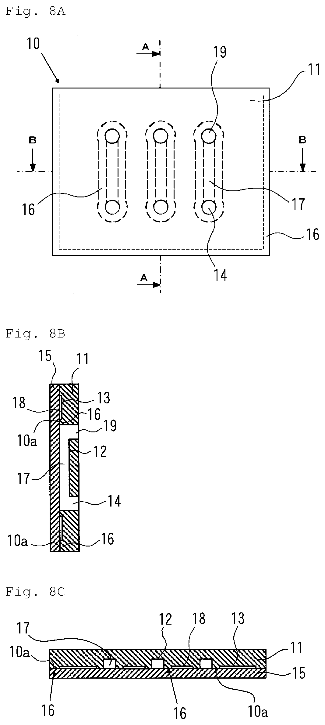
[0033] FIG. 3 is an explanatory cross-sectional view illustrating a first substrate and a second substrate before bonding.
[0034] FIG. 4 is an explanatory diagram illustrating a configuration according to a second embodiment of the microchip of the present invention.
[0035] FIG. 5 is an explanatory cross-sectional view illustrating, in an enlarged manner, essential parts of a modification of the microchip according to the first embodiment.
[0036] FIG. 6 is an explanatory cross-sectional view illustrating, in an enlarged manner, essential parts of a modification of the microchip according to the second embodiment.
[0037] FIG. 7 is an explanatory cross-sectional view illustrating, in an enlarged manner, essential parts of another modification of the microchip according to the first embodiment.
[0038] FIG. 8A is a plan view illustrating a configuration according to another embodiment of the microchip of the present invention.
[0039] FIG. 8B is a cross-sectional end view taken along line A-A of FIG. 8A.
[0040] FIG. 8C is a cross-sectional end view taken along line B-B of FIG. 8A.
[0041] FIG. 9 is an explanatory cross-sectional view illustrating, in an enlarged manner, essential parts of yet another modification of the microchip according to the first embodiment.
[0042] FIG. 10A is a plan view illustrating a configuration according to an example of a conventional microchip.
[0043] FIG. 10B is a cross-sectional end view taken along line A-A of FIG. 10A.
[0044] FIG. 10C is a cross-sectional end view taken along line B-B of FIG. 10A.
DESCRIPTION OF EMBODIMENTS
[0045] Embodiments of a microchip according to the present invention will be described below.
First Embodiment
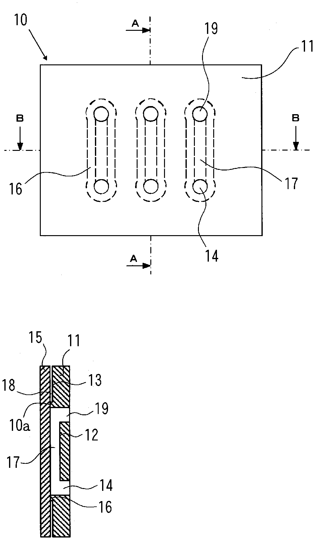
[0046] FIG. 1A is a plan view illustrating a configuration according to a first embodiment of the microchip of the present invention. FIG. 1B is a cross-sectional end view taken along line A-A of FIG. 1A. FIG. 1C is a cross-sectional end view taken along line B-B of FIG. 1A. This microchip 10 includes a plate-shape member formed by bonding a first substrate 11 made of a resin and a second substrate 15 made of a resin.
[0047] Channel forming steps 12 are formed in the front surface of the first substrate 11 on the side being in contact with the second substrate 15 (bottom surface in FIG. 1C). On the other hand, the front surface of the second substrate 15 on the side being in contact with the first substrate 11 (top surface in FIG. 1C) is configured as a flat surface. In the microchip 10, the channel forming steps 12 formed in the first substrate 11 form channels 17 surrounded by bonding portions 16 between the first substrate 11 and the second substrate 15. One end of each channel 17 is connected to an injection port 14 formed in the first substrate 11, and the other end of the channel 17 is connected to a discharge port 19 formed in the first substrate 11.
[0048] In addition, a noncontact portion step 13 is formed in the front surface of the first substrate 11 on the side being in contact with the second substrate 15 to surround the bonding portions 16. The noncontact portion step 13 forms a noncontact portion 18 surrounding the bonding portions 16 between the first substrate 11 and the second substrate 15.
[0049] Silicone resins, such as polydimethylsiloxane, cycloolefin resins and acrylic resins may be used as a resin constituting the first substrate 11 and the second substrate 15.
[0050] The thickness of each of the first substrate 11 and the second substrate 15 is not limited in particular. For example, the thickness is 0.5 to 7 mm.
[0051] The channels 17 have a width (in the illustrated example, the width of the channel forming steps 12) of 0.1 to 3 mm, for example.
[0052] The channels 17 have a height (in the illustrated example, the depth of the channel forming steps 12) of 0.05 to 1 mm, for example.
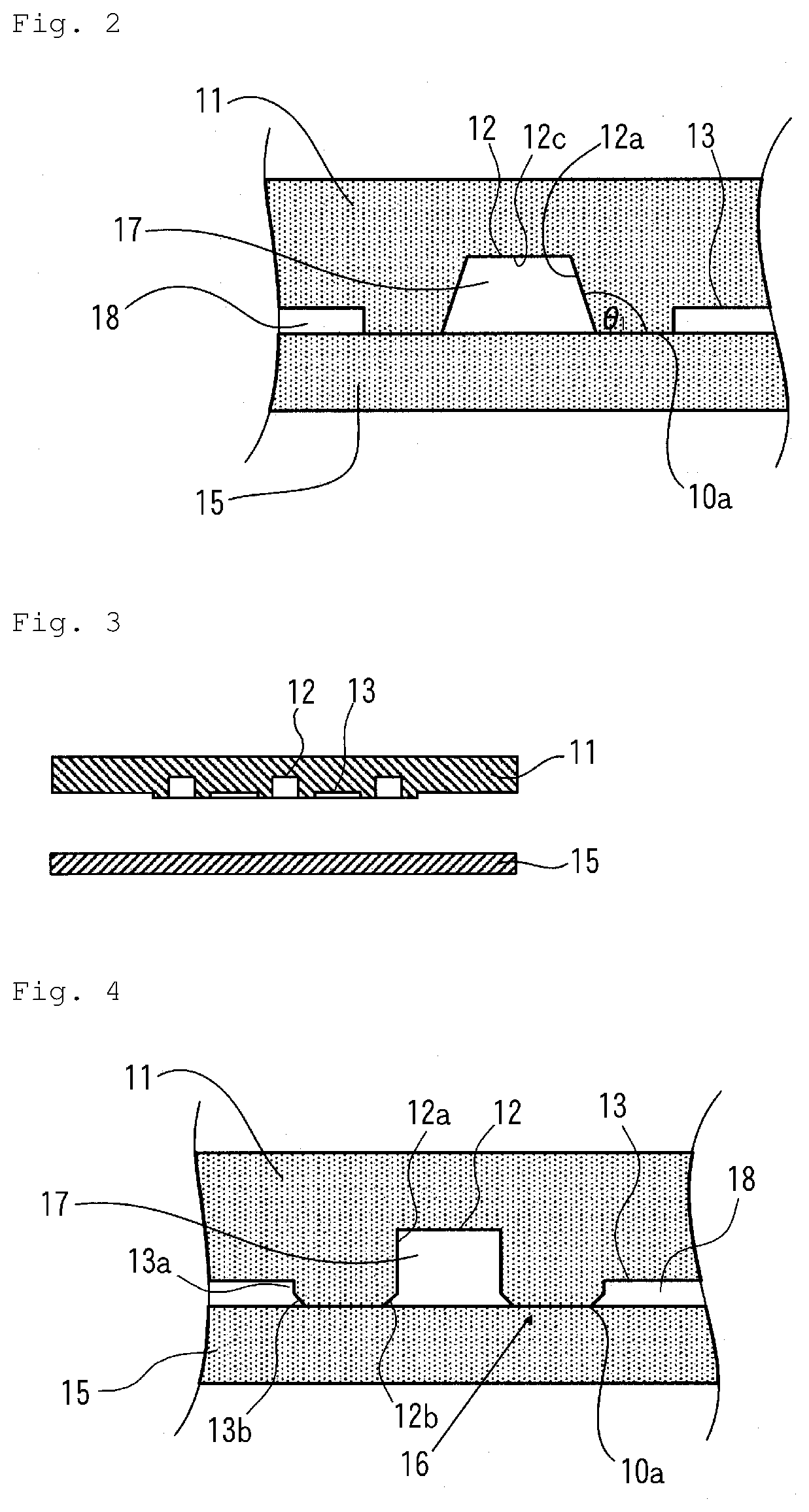
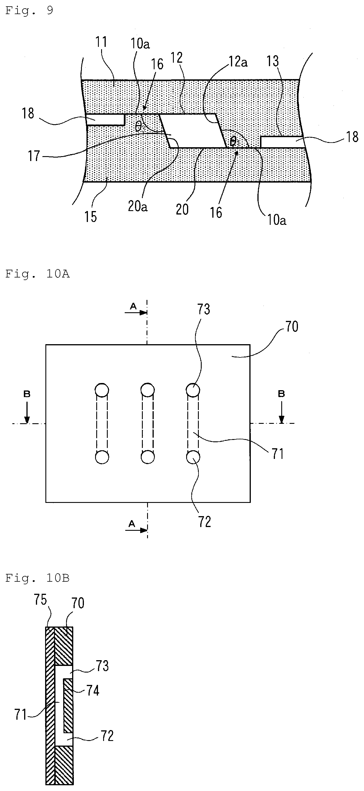
[0053] In the microchip 10 according to the present invention, as illustrated in an enlarged manner in FIG. 2, an angle .theta..sub.1 formed between each of the side wall surfaces 12a of the channel forming steps 12 and the bonding surface 10a continuous therewith (hereinafter, referred to simply as an "angle .theta..sub.1") satisfies .theta..sub.1>90.degree., preferably 120.degree..gtoreq..theta..sub.1>90.degree., more preferably 100.degree..gtoreq..theta..sub.1>90.degree.. If the angle .theta..sub.1 is not more than 90.degree., the first substrate 11 can fail to be released from a mold in manufacturing the first substrate 11 by injection molding. If the first substrate 11 is released from the mold by application of a large force in a direction of pulling the first substrate 11 and the mold apart, the vicinities of the continuous portions between the side wall surfaces 12a and the bonding surfaces 10a are deformed. This impairs the flatness of the bonding surfaces 10a and makes bonding over the entire bonding surfaces 10a difficult. Even if a combination of molds and the like can be contrived to mold the first substrate 11 configured to have an angle .theta..sub.1 of not more than 90.degree., sufficient pressure cannot be applied to the bonding surfaces 10a during the pressure treatment since the bonding surfaces 10a are unable to be pressed from directly above. This causes problems such as a drop in bonding strength. On the other hand, if the angle .theta..sub.1 is too large, bottom portions 12c of the channel forming steps 12 (top surface of the channel 17 in FIG. 2) decrease in area. Since the proportion of the side wall surfaces 12a that are slopes in the channels 17 increase, variations occur due to the velocity distribution of the circulated specimen, differences in reaction speed, etc. This makes impossible a predetermined action such as a biochemical reaction of the specimen to be caused in the channels 17. If optical observation under an optical microscope is performed, the side wall surfaces 12a are difficult to observe because of refraction. Since the observable regions are only the bottom portions 12c of reduced area, there also arise problems such as that accurate observation is not possible.
[0054] When the microchip 10 is seen in a plan view, the area S.sub.1 of the microchip 10 and the area S.sub.2 of the bonding surfaces 10a may preferably satisfy S.sub.2/S.sub.1<0.5, more preferably 0.03<S.sub.2/S.sub.1<0.3. If the value of the S.sub.2/S.sub.1 is not smaller than 0.5, the large bonding area makes absorption of warps and undulations difficult. To obtain a favorable bonding state with a large bonding area, the pressing force needs to be increased in the pressure treatment or the heating temperature needs to be increased in a heating treatment. As a result, the channels 17 are deformed. On the other hand, if the value of S.sub.2/S.sub.1 is too small, the bonding surfaces 10a themselves are small and thus the first substrate 11 and the second substrate 15 bonded by mechanical stress become more likely to exfoliate. In addition, application of a small load may increase the pressure at the bonding surfaces 10a, whereby the bonding portions 16 may be crushed or cracked.
[0055] The bonding surfaces 10a between the channels 17 and the noncontact portion 18 may preferably have a width of not less than 50 .mu.m, more preferably 500 to 2000 .mu.m. If the width of the bonding surfaces 10a is less than 50 .mu.m, the bonding surfaces 10a themselves are small and thus the first substrate 11 and the second substrate 15 bonded by mechanical stress become more likely to exfoliate. In addition, application of a small load can increase the pressure at the bonding surfaces 10a, whereby the bonding portions 16 can be crushed or cracked.
[0056] The foregoing microchip 10 can be manufactured, for example, in the following manner.
[0057] Initially, as illustrated in FIG. 3, the first substrate 11 and the second substrate 15 each made of a resin are manufactured. The channel forming steps 12 and the noncontact portion step 13 are formed in the front surface of the first substrate 11. On the other hand, the second substrate 15 is a flat front surface.
[0058] As a method for manufacturing the first substrate 11 and the second substrate 15, resin molding methods such as injection molding and casting can be selected as appropriate depending on the resin to be used.
[0059] Next, a surface activation treatment is performed on the front surfaces of the respective first and second substrates 11 and 15 to be bonding surfaces. For the surface activation treatment, an ultraviolet irradiation treatment of irradiating the front surfaces with vacuum ultraviolet rays having a wavelength of not more than 200 nm or a plasma treatment of bringing the front surfaces into contact with atmospheric pressure plasma from an atmospheric pressure plasma device can be used.
[0060] If the ultraviolet irradiation treatment is used as the surface activation treatment, an excimer lamp, such as a xenon excimer lamp having a bright line at a wavelength of 172 nm, a low-pressure mercury lamp having a center wavelength of 185 nm and a heavy hydrogen lamp having strong emission spectra within a range of 120 to 200 nm in wavelength can be suitably used as a light source for emitting vacuum ultraviolet rays.
[0061] The vacuum ultraviolet rays with which the front surfaces of the respective first and second substrates 11 and 15 are irradiated have an irradiance of 10 to 500 mW/cm.sup.2, for example.
[0062] The irradiation time of the front surfaces of the respective first and second substrates 11 and 15 with the vacuum ultraviolet rays are set as appropriate depending on the resin constituting the first substrate 11 and the second substrate 15. Examples include 5 to 6 seconds.
[0063] If the plasma treatment is used as the surface activation treatment, a plasma generation gas mainly containing nitrogen gas, argon gas, or the like containing 0.01 to 5 vol. % of oxygen gas is suitably used. Alternatively, a mixed gas of nitrogen gas and clean dry air (CDA) can be used.
[0064] The operation condition of the atmospheric pressure plasma device used in the plasma treatment includes, for example, a frequency of 20 to 70 kHz, a voltage of 5 to 15 kVp-p and a power value of 0.5 to 2 kW.
[0065] The processing time in the atmospheric pressure plasma is 5 to 100 seconds, for example.
[0066] The first substrate 11 and the second substrate 15 thus given the surface activation treatment are stacked so that their front surfaces are in contact with each other. The first substrate 11 and the second substrate 15 are then bonded by being pressed in a thickness direction by their own weights or by application of pressure from outside and, if needed, with application of heat.
[0067] Specific conditions of the foregoing pressurization and heating are set as appropriate depending on the material constituting the first substrate 11 and the second substrate 15.
[0068] Examples of the specific conditions include a pressing force of 0.1 to 10 MPa and a heating temperature of 40.degree. C. to 130.degree. C.
[0069] In the foregoing microchip 10, the noncontact portion 18 is formed to surround the bonding portions 16 formed around the channels 17, and the angle .theta..sub.1 satisfies .theta..sub.1>90.degree.. In bonding the first substrate 11 and the second substrate 15, pressure is thus concentrated on the portions of the first substrate 11 and the second substrate 15 to be the bonding portions 16. As a result, even if the first substrate 11 and the second substrate 15 are warped, their front surfaces to be the bonding surfaces are bonded in a fully close-contact state.
[0070] According to the microchip 10 of the present invention, a favorable bonding state can thus be achieved in the bonding portions 16 between the first substrate 11 and the second substrate 15 even if the microchip 10 is large in size. Since the pressing force, the heating temperature, or the heating time does not need to be increased in manufacturing the microchip 10, the channels 17 of desired configuration can be reliably formed.
[0071] FIG. 4 is an explanatory cross-sectional view illustrating a configuration of essential parts according to a second embodiment of the microchip of the present invention. This microchip 10 has the same configuration as that of the microchip 10 according to the first embodiment except the following aspects:
[0072] In the microchip illustrated in FIG. 4, the side wall surfaces 12a of the channel forming steps 12 and the side wall surfaces 13a of the noncontact portion 18 are chamfered in areas (hereinafter, also referred to as "bonding portion neighboring areas") 12b and 13b near the bonding surfaces 10a continuous with the respective side wall surfaces 12a and 13a.
[0073] The angle .theta..sub.1 is within a range of 140.degree..gtoreq..theta..sub.1.gtoreq.90.degree., for example.
[0074] In the foregoing microchip 10, the noncontact portion 18 is formed to surround the bonding portions 16 formed around the channels 17, and the side wall surfaces 12a of the channel forming steps 12 and the side wall surfaces 13a of the noncontact portion 18 are chamfered in the respective bonding portion neighboring areas 12b and 13b. In bonding the first substrate 11 and the second substrate 15, pressure is thus concentrated on the portions of the first substrate 11 and the second substrate 15 to be the bonding portions 16. As a result, even if the first substrate 11 and the second substrate 15 are warped, their front surfaces to be the bonding surfaces can be bonded in a fully close-contact state.
[0075] According to the microchip 10 of the present invention, a favorable bonding state can be achieved in the bonding portions 16 between the first substrate 11 and the second substrate 15 even if the microchip 10 is large in size. In addition, since the pressing force, the heating temperature, or the heating time does not need to be increased in manufacturing the microchip 10, the channels 17 of desired configuration can be reliably formed.
[0076] While the first embodiment and the second embodiment according to the microchip of the present invention have been described above, the present invention is not limited to such embodiments, and various modifications can be made as follows:
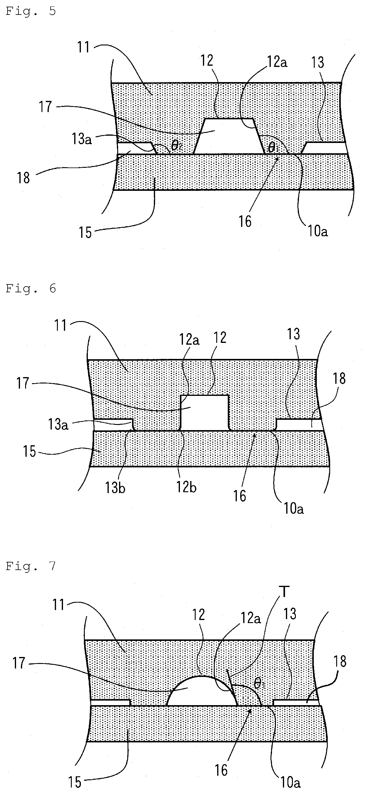
[0077] (1) In the first embodiment, as illustrated in FIG. 5, an angle .theta..sub.2 formed between each of the side wall surfaces 13a of the noncontact portion 18 and the bonding surface 10a continuous therewith (hereinafter, referred to simply as an "angle .theta..sub.2") may preferably satisfy .theta..sub.2>90.degree., more preferably 150.degree..gtoreq..theta..sub.2>90.degree., yet more preferably 120.degree..gtoreq..theta..sub.2>90.degree..
[0078] According to such a microchip 10, in bonding the first substrate 11 and the second substrate 15, pressure is even more concentrated on the portions of the first substrate 11 and the second substrate 15 to be the bonding portions 16. A favorable bonding state can thus be more reliably achieved in the bonding portions 16 between the first substrate 11 and the second substrate 15 even if the microchip 10 is large in size.
[0079] (2) In the second embodiment, as illustrated in FIG. 6, the side wall surfaces 12a of the channel forming steps 12 and the side wall surfaces 13a of the noncontact portion 18 may be rounded in the respective bonding portion neighboring areas 12b and 13b instead of being chamfered.
[0080] (3) In the microchips 10 illustrated in FIGS. 4 and 6, either the side wall surfaces 12a of the channel forming steps 12 or the side wall surfaces 13a of the noncontact portion 18 may be chamfered or rounded in the bonding portion neighboring areas 12b or the bonding portion neighboring areas 13b.
[0081] (4) In the first embodiment, the bottom surface and the side wall surfaces 12a of a channel forming step 12 are configured as a flat surface each. However, as illustrated in FIG. 7, the bottom surface and the side wall surfaces 12a may be configured as a continuous curved surface. In such a configuration, the angle .theta..sub.1 refers to an angle formed between the tangent T to the side wall surface 12a of the channel forming step 12 at the intersection of the side wall surface 12a and the bonding surface 10a and the bonding surface 10a in a section perpendicular to the extending direction of the channel 17.
[0082] (5) According to the microchip 10 of the present invention, as illustrated in FIGS. 8A to 8C, a bonding portion 16 between the first substrate 11 and the second substrate 15 may be formed at least on part of the periphery of the first substrate 11 and the second substrate 15 (in the illustrated example, the entire periphery).
[0083] In such a configuration, the bonding surface 10a formed on the periphery of the first substrate 11 and the second substrate 15 may preferably have a width of not less than 50 .mu.m, more preferably 500 to 3000 .mu.m. The bonding surface 10a formed on the foregoing periphery is desirably bonded over a width greater than that of the bonding surfaces 10a between the channels 17 and the noncontact portion 18. According to such a configuration, the microchip 10 is more tolerable against mechanical stress acting in a direction in which the first substrate 11 and the second substrate 15 exfoliate.
[0084] The area S.sub.2 of the bonding surfaces 10a refers to a total of the areas of the bonding surfaces 10a between the channels 17 and the noncontact portion 18 and the area of the bonding surface 10a formed on the periphery of the first substrate 11 and the second substrate 15.
[0085] (6) In the first embodiment, as illustrated in FIG. 9, a channel 17 maybe formed by a channel forming step 12 formed in the first substrate 11 and a channel forming step 20 formed in the second substrate 15.
[0086] In such a configuration, like the angle .theta..sub.1, an angle .theta..sub.3 formed between a side wall surface 20a of the channel forming step 20 in the second substrate 15 and the bonding surface 10a continuous therewith satisfies .theta..sub.3>90.degree., preferably 120.degree..gtoreq..theta..sub.3>90.degree., more preferably 100.degree..gtoreq..theta..sub.3>90.degree..
[0087] (7) Each of the microchips 10 illustrated in FIGS. 1 to 9 is an example where the noncontact portion 18 is formed separately from the channels 17. However, the microchip according to the present invention may be configured so that the noncontact portion also serves as a channel.
REFERENCE SIGNS LIST
[0088] 10 microchip [0089] 10a bonding surface [0090] 11 first substrate [0091] 12 channel forming step [0092] 12a side wall surface [0093] 12b bonding portion neighboring area [0094] 12c bottom portion [0095] 13 noncontact portion step [0096] 13a side wall surface [0097] 13b bonding portion neighboring area [0098] 14 injection port [0099] 15 second substrate [0100] 16 bonding portion [0101] 17 channel [0102] 18 noncontact portion [0103] 19 discharge port [0104] 20 channel forming step [0105] 20a side wall surface [0106] 70 first substrate [0107] 71 channel [0108] 72 injection port [0109] 73 discharge port [0110] 74 channel forming step [0111] 75 second substrate
* * * * *
D00000
D00001
D00002
D00003
D00004
D00005
D00006
XML
uspto.report is an independent third-party trademark research tool that is not affiliated, endorsed, or sponsored by the United States Patent and Trademark Office (USPTO) or any other governmental organization. The information provided by uspto.report is based on publicly available data at the time of writing and is intended for informational purposes only.
While we strive to provide accurate and up-to-date information, we do not guarantee the accuracy, completeness, reliability, or suitability of the information displayed on this site. The use of this site is at your own risk. Any reliance you place on such information is therefore strictly at your own risk.
All official trademark data, including owner information, should be verified by visiting the official USPTO website at www.uspto.gov. This site is not intended to replace professional legal advice and should not be used as a substitute for consulting with a legal professional who is knowledgeable about trademark law.