Semiconductor Packages And Methods Of Manufacturing The Same
Kind Code
U.S. patent application number 16/264599 was filed with the patent office on 2020-08-06 for semiconductor packages and methods of manufacturing the same. This patent application is currently assigned to Advanced Semiconductor Engineering, Inc.. The applicant listed for this patent is Advanced Semiconductor Engineering, Inc.. Invention is credited to Chen Yuang CHEN, Chun Chen CHEN, Jiming LI, Yuanhao YU.
| Application Number | 20200251421 16/264599 |
| Document ID | / |
| Family ID | 1000003883188 |
| Filed Date | 2020-08-06 |


View All Diagrams
| United States Patent Application | 20200251421 |
| Kind Code | A1 |
| CHEN; Chen Yuang ; et al. | August 6, 2020 |
SEMICONDUCTOR PACKAGES AND METHODS OF MANUFACTURING THE SAME
Abstract
A semiconductor package includes a substrate, a preformed feeding element, a preformed shielding element, and an encapsulant. The preformed feeding element is disposed on the substrate and the preformed feeding element is disposed on the substrate and adjacent to the preformed feeding element. The encapsulant encapsulates the preformed feeding element and the preformed shielding element.
| Inventors: | CHEN; Chen Yuang; (Kaohsiung, TW) ; LI; Jiming; (Kaohsiung, TW) ; CHEN; Chun Chen; (Kaohsiung, TW) ; YU; Yuanhao; (Kaohsiung, TW) | ||||||||||
| Applicant: |
|
||||||||||
|---|---|---|---|---|---|---|---|---|---|---|---|
| Assignee: | Advanced Semiconductor Engineering,
Inc. Kaohsiung TW |
||||||||||
| Family ID: | 1000003883188 | ||||||||||
| Appl. No.: | 16/264599 | ||||||||||
| Filed: | January 31, 2019 |
| Current U.S. Class: | 1/1 |
| Current CPC Class: | H01L 21/565 20130101; H01Q 1/526 20130101; H01L 23/552 20130101; H01L 21/4853 20130101; H01Q 1/2283 20130101; H01L 23/49838 20130101; H01L 2224/16227 20130101; H01L 2924/3025 20130101; H01L 2223/6677 20130101; H01L 23/3121 20130101; H01L 23/66 20130101; H01L 24/16 20130101 |
| International Class: | H01L 23/552 20060101 H01L023/552; H01L 23/31 20060101 H01L023/31; H01L 23/498 20060101 H01L023/498; H01L 23/66 20060101 H01L023/66; H01L 23/00 20060101 H01L023/00; H01L 21/48 20060101 H01L021/48; H01L 21/56 20060101 H01L021/56; H01Q 1/22 20060101 H01Q001/22; H01Q 1/52 20060101 H01Q001/52 |
Claims
1. A semiconductor package, comprising: a substrate; a preformed feeding element disposed on the substrate; a preformed shielding element disposed on the substrate and adjacent to the preformed feeding element; and an encapsulant encapsulating the preformed feeding element and the preformed shielding element.
2. The semiconductor package of claim 1, wherein the encapsulant includes a first space accommodating the preformed feeding element and a second space accommodating the preformed shielding element, the first space is defined by the preformed feeding element, and the second space is defined by the preformed shielding element.
3. The semiconductor package of claim 1, wherein the encapsulant includes fillers and the fillers adjacent to the preformed feeding element and the preformed shielding element are intact.
4. The semiconductor package of claim 1, wherein the preformed shielding element surrounds the preformed feeding element.
5. The semiconductor package of claim 4, wherein the preformed shielding element includes at least one opening.
6. The semiconductor package of claim 4, wherein the preformed shielding element includes a plurality of pieces spacing apart from each other.
7. The semiconductor package of claim 1, further comprising an antenna layer disposed adjacent to the preformed feeding element and the preformed shielding element and electrically connected to the preformed feeding element and the preformed shielding element.
8. The semiconductor package of claim 7, further comprising a connector disposed on the preformed feeding element and the preformed shielding element to connect the preformed feeding element and the preformed shielding element to the antenna layer.
9. The semiconductor package of claim 1, further comprising a semiconductor component and a compartment disposed on the substrate, the semiconductor component and the preformed feeding element are separated by the compartment.
10. The semiconductor package of claim 9, further comprising a shielding layer disposed on the encapsulant to connect electrically to the compartment.
11. A semiconductor package, comprising: a substrate; and a RF structure disposed on the substrate, the RF structure including a feeding element and a shielding element adjacent to the feeding element; wherein a pitch from the feeding element to the shielding element is about 1000 .mu.m to about 1500 .mu.m with the insertion loss.gtoreq.-0.5 dB under about 0.5 GHz to about 70 GHz.
12. The semiconductor package of claim 11, wherein the pitch is about 1000 .mu.m to about 1200 .mu.m.
13. The semiconductor package of claim 11, wherein the pitch is about 1300 .mu.m to about 1500 .mu.m with the insertion loss .gtoreq.-0.5 dB under about 0.5 GHz to about 60 GHz.
14. The semiconductor package of claim 11, wherein the shielding element surrounds the feeding element.
15. A semiconductor package, comprising: a substrate; and a RF structure disposed on the substrate, the RF structure including a feeding element and a shielding element adjacent to the feeding element; wherein a pitch from the feeding element to the shielding element is about 1000 .mu.m to about 1500 .mu.m with the return loss.ltoreq.-10 dB under about 0.5 MHz to about 80 MHz.
16. The semiconductor package of claim 15, wherein the pitch from the feeding element to the shielding element is about 1300 .mu.m to 1500 .mu.m with the return loss.ltoreq.-10 dB under about 0.5 MHz to about 60 MHz.
17. The semiconductor package of claim 15, wherein the shielding element surrounds the feeding element.
18. A semiconductor package, comprising: a substrate; and a RF structure disposed on the substrate, the RF structure including a feeding element and a shielding element adjacent to the feeding element; wherein a pitch from the feeding element to the shielding element is about 0 .mu.m<Pitch.ltoreq.800 .mu.m with the insertion loss.gtoreq.-0.5 dB under about 60 GHz to about 75 GHz.
19. The semiconductor package of claim 18, wherein the shielding element surrounds the feeding element.
20. A semiconductor package, comprising: a substrate; and a RF structure disposed on the substrate, the RF structure including a feeding element and a shielding element adjacent to the feeding element; wherein a pitch from the feeding element to the shielding element is about 0 .mu.m<Pitch.ltoreq.800 .mu.m with the return loss.ltoreq.-10 dB under about 0.5 MHz to about 80 MHz.
21. The semiconductor package of claim 20, wherein the shielding element surrounds the feeding element.
22. A method of manufacturing a semiconductor package, comprising: forming a RF structure on a substrate, the RF structure including a feeding element and a shielding element adjacent to the feeding element; and molding the substrate, the feeding element, and the shielding element to form an encapsulant.
23. The method of claim 22, further comprising: exposing the RF structure from the encapsulant; and providing an antenna layer on the RF structure.
24. The method of claim 22, further comprising: disposing a connector on the RF structure to connect the RF structure to the antenna layer.
25. The method of claim 22, wherein the encapsulant includes fillers and encapsulate the substrate, the feeding element, and the shielding element.
Description
BACKGROUND
1. Technical Field
[0001] The present disclosure relates to semiconductor packages and method of manufacturing the same, and, more particularly, to semiconductor packages including at least two semiconductor components and method of manufacturing the same.
2. Description of the Related Art
[0002] There is a continuing desire to incorporate more than one semiconductor component into a single semiconductor package to reduce dimensions of the package. A semiconductor package incorporating multiple semiconductor components may be referred to as a system in package (SiP). Because semiconductor components in a semiconductor package specify electrical connections to an external environment, such electrical connections and the process for making the same are important in determining whether the semiconductor components can function properly or can achieve specified performances.
SUMMARY
[0003] In an embodiment, a semiconductor package includes a substrate; a preformed feeding element; a preformed shielding element; and an encapsulant. The preformed feeding element is disposed on the substrate and the preformed feeding element is disposed on the substrate and adjacent to the preformed feeding element. The encapsulant encapsulates the preformed feeding element and the preformed shielding element.
[0004] In an embodiment, a semiconductor package includes a substrate and a RF structure. The RF structure is disposed on the substrate and includes a feeding element and a shielding element adjacent to the feeding element, wherein a pitch from the feeding element to the shielding element is about 1000 .mu.m to about 1500 .mu.m with the insertion loss.gtoreq.-0.5 dB under about 0.5 GHz to about 70 GHz.
[0005] In an embodiment, a semiconductor package includes a substrate and a RF structure. The RF structure is disposed on the substrate and includes a feeding element and a shielding element adjacent to the feeding element, wherein a pitch from the feeding element to the shielding element is about 1000 .mu.m to about 1500 .mu.m with the return loss.ltoreq.-10 dB under about 0.5 MHz to about 80 MHz.
[0006] In an embodiment, a semiconductor package includes a substrate and a RF structure. The RF structure is disposed on the substrate and includes a feeding element and a shielding element adjacent to the feeding element, wherein a pitch from the feeding element to the shielding element is about 0 .mu.m<Pitch.ltoreq.about 800 .mu.m with the insertion loss.gtoreq.-0.5 dB under about 60 GHz to about 75 GHz.
[0007] In an embodiment, a semiconductor package includes a substrate and a RF structure. The RF structure is disposed on the substrate and includes a feeding element and a shielding element adjacent to the feeding element, wherein a pitch from the feeding element to the shielding element is about 0 .mu.m<Pitch.ltoreq.about 800 .mu.m with the return loss.ltoreq.-10 dB under about 0.5 MHz to about 80 MHz.
[0008] In an embodiment, a method of manufacturing includes (a) forming a RF structure on a substrate, the RF structure including a feeding element and a shielding element adjacent to the feeding element; and (b) molding the substrate, the feeding element and the shielding element.
BRIEF DESCRIPTION OF THE DRAWINGS
[0009] FIG. 1(a) illustrates a cross-sectional view of a semiconductor package according to an embodiment of the present disclosure.
[0010] FIG. 1(b) illustrates a top view of the second semiconductor component of FIG. 1(a) along with A-A line in accordance with an embodiment of the present disclosure.
[0011] FIG. 1(c) illustrates an enlarged view of an area B of the embodiment of a second semiconductor component illustrated in FIG. 1(a).
[0012] FIG. 2 illustrates a cross-sectional view of a semiconductor package according to an embodiment of the present disclosure.
[0013] FIG. 3(a) illustrates a cross-sectional view of a semiconductor package according to an embodiment of the present disclosure.
[0014] FIG. 3(b) illustrates an enlarged view of an area C of the conductive via of the embodiment of a third semiconductor component illustrated in FIG. 3(a).
[0015] FIG. 3(c) illustrates an enlarged view of an area D of the embodiment of a second semiconductor component illustrated in FIG. 3(a).
[0016] FIG. 4 illustrates a cross-sectional view of a semiconductor package according to an embodiment of the present disclosure.
[0017] FIG. 5 illustrates a cross-sectional view of a semiconductor package according to an embodiment of the present disclosure.
[0018] FIG. 6 illustrates a cross-sectional view of a semiconductor package according to an embodiment of the present disclosure.
[0019] FIG. 7 illustrates a cross-sectional view of a semiconductor package according to an embodiment of the present disclosure.
[0020] FIG. 8 illustrates a cross-sectional view of a semiconductor package according to an embodiment of the present disclosure.
[0021] FIG. 9 illustrates a cross-sectional view of a semiconductor package according to an embodiment of the present disclosure.
[0022] FIG. 10(a) illustrates a top view of a second semiconductor component in accordance with embodiments of the present disclosure.
[0023] FIG. 10(b) illustrates a top view of a second semiconductor component in accordance with embodiments of the present disclosure.
[0024] FIG. 11(a) illustrates a top view of a second semiconductor component in accordance with embodiments of the present disclosure.
[0025] FIG. 11(b) illustrates a top view of a second semiconductor component in accordance with embodiments of the present disclosure.
[0026] FIG. 11(c) illustrates a top view of a second semiconductor component in accordance with embodiments of the present disclosure.
[0027] FIG. 11(d) illustrates a top view of a second semiconductor component in accordance with embodiments of the present disclosure.
[0028] FIG. 11(e) illustrates a top view of a second semiconductor component in accordance with embodiments of the present disclosure.
[0029] FIG. 12(a) and FIG. 12(b) illustrate a method for manufacturing a semiconductor package such as the semiconductor package of FIG. 1(a).
[0030] FIG. 12(a), FIG. 12(b), and FIG. 12(c) illustrate a method for manufacturing a semiconductor package such as the semiconductor package of FIG. 3(a).
[0031] FIG. 12(a), FIG. 12(b), FIG. 12(c), and FIG. 12(d) illustrate a method for manufacturing a semiconductor package such as the semiconductor package of FIG. 4.
[0032] FIG. 12(a), FIG. 12(b), FIG. 12(c), FIG. 12(d), and FIG. 12(e) illustrate a method for manufacturing a semiconductor package such as the semiconductor package of FIG. 5.
[0033] FIG. 12(a), FIG. 12(b), FIG. 12(c), FIG. 12(d), FIG. 12(e), and FIG. 12(f) illustrate a method for manufacturing a semiconductor package such as the semiconductor package of FIG. 7.
DETAILED DESCRIPTION
[0034] Spatial descriptions, such as "top," "side," "over," and so forth, are indicated with respect to the orientation shown in the figures unless otherwise specified. It should be understood that the spatial descriptions used herein are for purposes of illustration only, and that practical implementations of the structures described herein can be spatially arranged in any orientation or manner, provided that the merits of embodiments of this disclosure are not deviated by such arrangement.
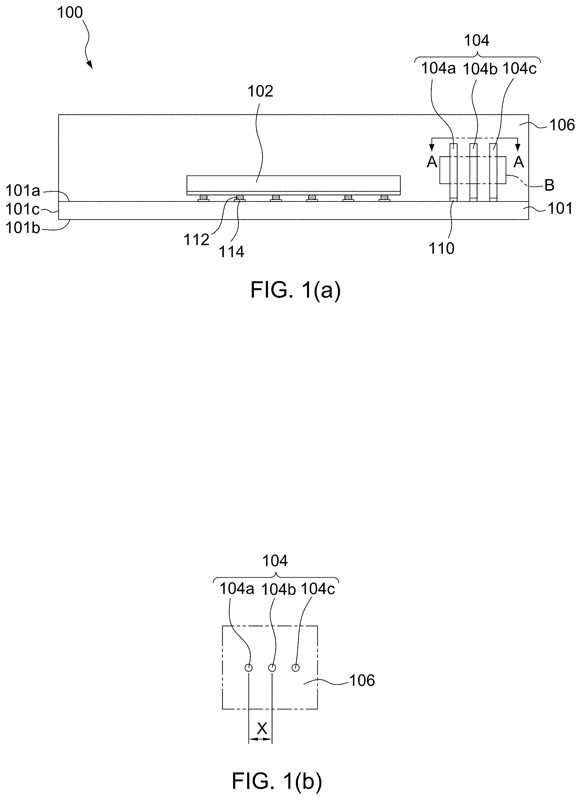
[0035] FIG. 1(a) illustrates a cross-sectional view of a semiconductor package 100 according to an embodiment of the present disclosure. The semiconductor package 100 includes a substrate 101, a first semiconductor component 102, a second semiconductor component 104, and an encapsulant 106.
[0036] The substrate 101 has a first surface 101a, a second surface 101b, and a side surface 101c. The first surface 101a is opposite to the second surface 101b. The side surface 101c extends between the first surface 101a and the second surface 101b. In the embodiment illustrated in FIG. 1(a), the substrate 101 includes at least one bonding pad 114 disposed adjacent to the first surface 101a of the substrate 101. The bonding pad 114 may be, for example, a contact pad of a trace. In the embodiment of FIG. 1(a), the first surface 101a is an active surface, the bonding pad 114 is a contact pad, and the bonding pad 114 is disposed directly (e.g., in physical contact) on the first surface 101a of the substrate 101. The bonding pad 114 may include, for example, copper, gold, indium, tin, silver, palladium, osmium, iridium, ruthenium, titanium, magnesium, aluminum, cobalt, nickel, or zinc, other metals, metal alloys, or a combination of two or more thereof.
[0037] The first semiconductor component 102 is disposed on the first surface 101a of the substrate 101. The first semiconductor component 102 may be any semiconductor component including, for example, a chip, a package, an interposer, or a combination thereof. In the embodiment illustrated in FIG. 1(a), the first semiconductor component 102 is a chip including at least one conductive connector 112. The first conductive connector 112 contacts the bonding pad 114. The conductive connector 112 may be, for example, a pillar structure, which may include an under bump metallization (UBM) layer, a pillar, a barrier layer, a solder layer, or a combination of two or more thereof, or solder/stud bumps.
[0038] The second semiconductor component 104 is disposed on the first surface 101a of the substrate 101. The second semiconductor component 104 may be any semiconductor component including, for example, a RF structure. A RF structure may include at least one feeding element and at least one shielding element. According to the present disclosures, the feeding element and the shielding element were pre-formed so that their properties can be pre-determined and formed in any desired shape, for example, including square-like, triangular-like, round-like, rectangular-like, pentagonal-like, hexagonal-like, heptagonal-like, octagonal-like, trapezoidal-like, oval-like, rhombic-like, or parallelogram-like column shape. Unlike a feeding via or shielding via or ground via formed by photolithography in combination with etching (or drilling) and electroplating on a substrate, where the shape of the via fully depends on the drilling or etching technology and the properties of the via fully depends on the electroplating technology, the feeding element and the shielding element according to the embodiments of the present disclosures are pre-formed, for example, by molding, where their shape and properties can be controlled. Therefore, the voids in the feeding via or shielding via or ground via caused by electroplating can be avoided, which can reduce the signal loss.
[0039] In the embodiment illustrated in FIG. 1(a), the second semiconductor component 104 includes at least one preformed feeding element 104b disposed on the first surface 101a of the substrate 101 and at least one preformed shielding element 104a, 104c disposed on the first surface 101a of the substrate 101 and adjacent to the preformed feeding element 104b. The preformed feeding element 104b and the preformed shielding element 104a, 104c are spaced from each other by a distance. The shielding element 104a, 104c may include a plurality of pieces 104a, 104c spacing apart from each other. The feeding element 104b and the shielding element 104a, 104c may be disposed on the substrate 101 by a surface mount technology (SMT). In the embodiment illustrated in FIG. 1, the feeding element 104b and the shielding element 104a, 104c are disposed on the substrate 101 by a surface mount technology (SMT) with a solder paste 110.
[0040] The encapsulant 106 is disposed between the first semiconductor component 102 and the second semiconductor component 104. The encapsulant 106 encapsulates the preformed feeding element 104b and the preformed shielding element 104a, 104c. In the embodiment illustrated in FIG. 1(a), the preformed feeding element 104b defines a first space in the encapsulant 106 and the preformed shielding element 104a, 104c defines a second space in the encapsulant 106, where the encapsulant 106 surrounds them and accommodates the first space and the second space. The encapsulant 106 may extend from the preformed shielding element 104a to the first semiconductor component 102. The encapsulant 106 may cover the first semiconductor component 102, the preformed feeding element 104b, the preformed shielding element 104a, 104c, and the first surface 101a of the substrate 101, but not the side surface 101c of the substrate 101. The encapsulant 106 may be, for example, a solder mask (the material of which is, for example, polyimide (PI)), a passivation layer (the material of which is, for example, a metal oxide), or an underfill. The encapsulant 106 may include fillers, the material of which is, for example, silica and/or carbon for reducing stress on the die and warpage of a resulting semiconductor package.
[0041] FIG. 1(b) illustrates a top view of the second semiconductor component 104 of FIG. 1(a) along with A-A line in accordance with an embodiment of the present disclosure. The second semiconductor component 104 comprises one feeding element 104b and one shielding element 104a, 104c. The shielding element 104a, 104c surrounds the feeding element 104b. The shielding element 104a, 104c comprises two pieces 104a, 104c spacing apart from each other and includes at least one opening between them. The shielding element 104a, 104c are disposed adjacent to the feeding element 104b and are at the opposite sides of each other. The distance X from the center of the shielding element 104a, 104b to the center of the feeding element 104b (a pitch) is determined according to the desired properties of the second semiconductor component 104.
[0042] In an embodiment of the present disclosures, the pitch X can be about 1000 .mu.m to about 1500 .mu.m for a RF structure with an insertion loss.gtoreq.-0.5 dB under about 0.5 GHz to about 70 GHz.
[0043] In an embodiment of the present disclosures, the pitch X can be about 1000 .mu.m to about 1200 .mu.m for a RF structure with an insertion loss.gtoreq.-0.5 dB under about 0.5 GHz to about 70 GHz.
[0044] In an embodiment of the present disclosures, the pitch X can be about 1300 .mu.m to about 1500 .mu.m for a RF structure with an insertion loss.gtoreq.-0.5 dB under about 0.5 GHz to about 70 GHz.
[0045] In an embodiment of the present disclosures, the pitch X can be about 1000 .mu.m to about 1500 .mu.m for a RF structure with a return loss.ltoreq.-10 dB under about 0.5 MHz to about 80 MHz.
[0046] In an embodiment of the present disclosures, the pitch X can be about 1300 .mu.m to 1500 .mu.m with the return loss.ltoreq.-10 dB under about 0.5 MHz to about 60 MHz.
[0047] In an embodiment of the present disclosures, the pitch X can be about 0 .mu.m<Pitch.ltoreq.800 .mu.m with the insertion loss.gtoreq.-0.5 dB under about 60 GHz to about 75 GHz.
[0048] In an embodiment of the present disclosures, the pitch X can be about 0 .mu.m<Pitch.ltoreq.800 .mu.m with the return loss.ltoreq.-10 dB under about 60 MHz to about 80 MHz.
[0049] The feeding element 104b and the shielding element 104a, 104c are all surrounded by the encapsulant 106. The feeding element 104b and the shielding element 104a, 104c can be in different shape depending on the molding technology or the technology to be used to form them. In the embodiment illustrated in FIG. 1(b), an outer boundary of the feeding element 104b is similar to an outer boundary of the shielding element 104a and an outer boundary of the shielding element 104a can be similar to an outer boundary of the opposite shielding element 104c. In the embodiment illustrated in FIG. 1(b), the feeding element 104b and the shielding elements 104a, 104c have a round-like column shape
[0050] FIG. 1(c) illustrates an enlarged view of an area B of the embodiment of a second semiconductor component 104 illustrated in FIG. 1(a). In the embodiment illustrated in FIG. 1(c), the encapsulant 106 includes fillers 122. The fillers 122 are adjacent to the feeding element 104b and the shielding elements 104a, 104c. The fillers 122 may be in regular or irregular shape. In the embodiment illustrated in FIG. 1(c), the shape of the fillers 122 remain intact because the feeding element 104b and the shielding elements 104a, 104c are preformed in accordance with the embodiments of the present disclosures rather than formed by photolithography in combination with etching (or drilling) and electroplating. Therefore, the fillers 122 in the encapsulant 106 are not damaged by the etching or drilling and the shape thereof can remain intact. Accordingly, the effect of the fillers 122, such as reducing stress on the die and warpage of a resulting semiconductor package, will not be compromised and can be maintained.
[0051] FIG. 2 illustrates a cross-sectional view of a semiconductor package 200 according to an embodiment of the present disclosure. The semiconductor package 200 in FIG. 2 is similar to the semiconductor package 100 in FIG. 1, with differences including that the semiconductor package 200 includes a first encapsulant 216 and a second encapsulant 206. The first encapsulant 216 is adjacent to the second encapsulant 206. The first encapsulant 216 encapsulates the second semiconductor component 204. In particular, the first encapsulant 216 covers the preformed feeding element 204b, the preformed shielding element 204a, 204c, and the first surface 201a of the substrate 201, but not the side surface 201c of the substrate 201. The second encapsulant 206 covers the first semiconductor component 202 and the first surface 201a of the substrate 201, but not the side surface 201c of the substrate 201. The first encapsulant 216 and the second encapsulant 206 are composed of different materials. The first encapsulant 216 and the second encapsulant 206 may include fillers, the material of which is, for example, silica and/or carbon for reducing stress on the die and warpage of a resulting semiconductor package.
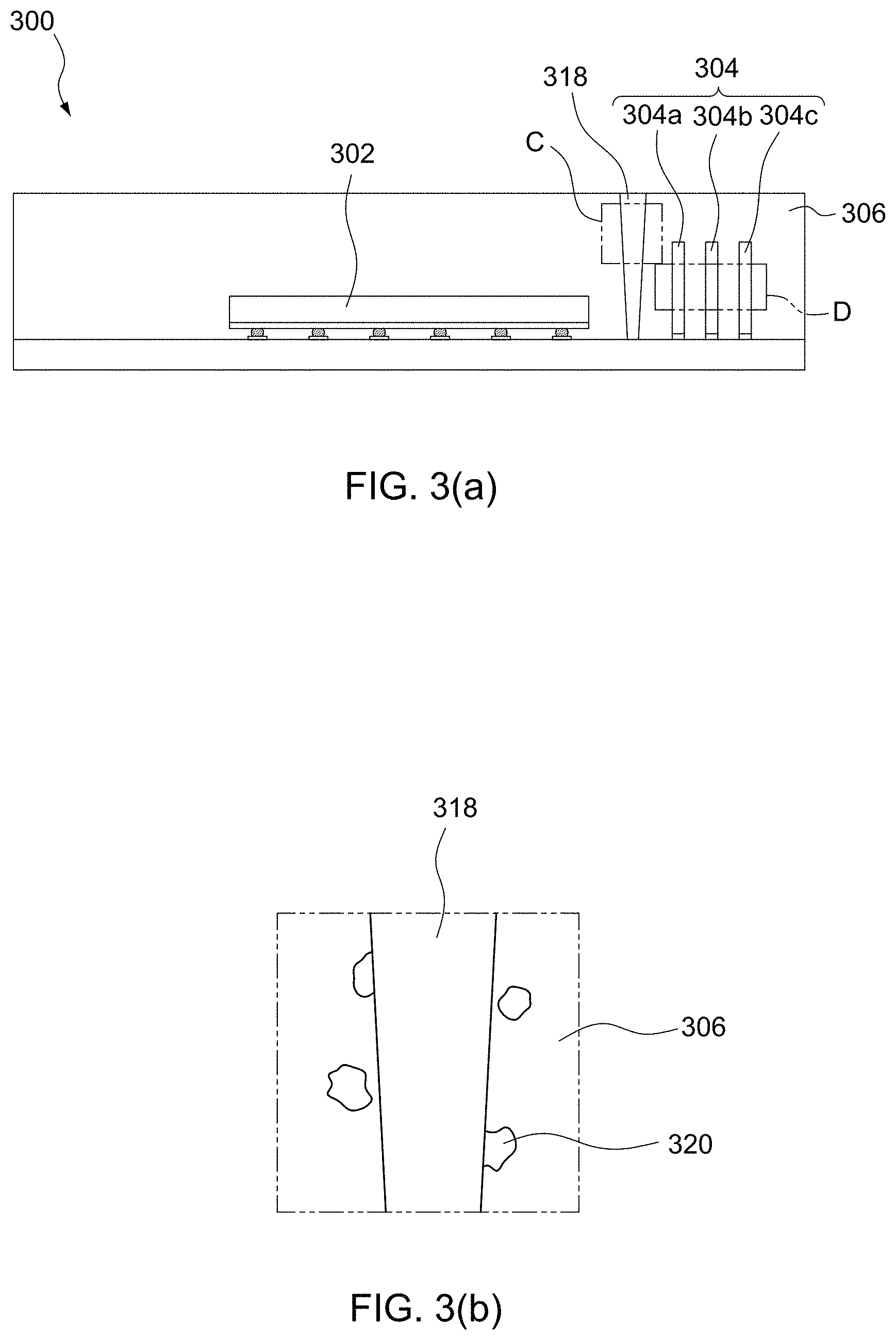
[0052] FIG. 3(a) illustrates a cross-sectional view of a semiconductor package 300 according to an embodiment of the present disclosure. The semiconductor package 300 in FIG. 3 is similar to the semiconductor package 100 in FIG. 1, with differences including that the semiconductor package 300 further includes a third semiconductor component 318 disposed in the encapsulant 306. The third semiconductor component 318 is disposed between the first semiconductor component 302 and the second semiconductor component 304. The third semiconductor component 318 may be, for example, a compartment separating the first semiconductor component 302 from the second semiconductor component 304, or a conductive via. In the embodiment illustrated in FIG. 3(a), the third semiconductor component 318 is a conductive via extending through the encapsulant 306 from the substrate 308 to the surface of the encapsulant 306 and formed by drilling (or etching) and electroplating.
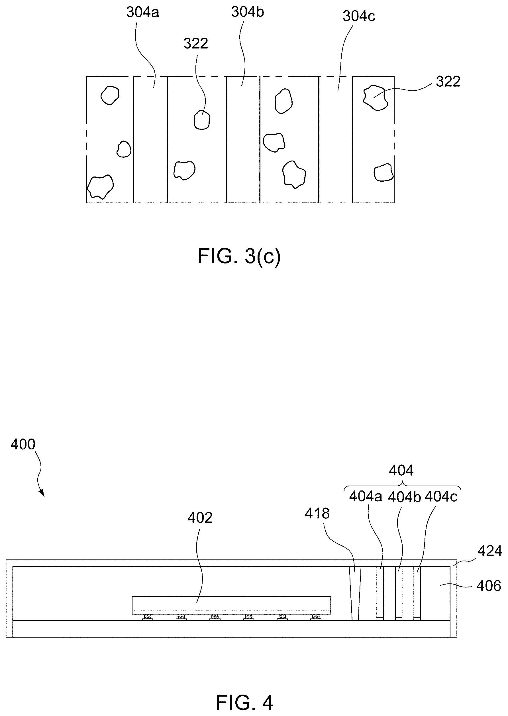
[0053] FIG. 3(b) illustrates an enlarged view of an area C of the conductive via 318 of the embodiment of a third semiconductor component 318 illustrated in FIG. 3(a). FIG. 3(c) illustrates an enlarged view of an area D of the embodiment of a second semiconductor component 304 illustrated in FIG. 3(a). The encapsulant 306 includes fillers 320 adjacent to the conductive via 318 and fillers 322 adjacent to the feeding element 304b and the shielding elements 304a, 304c. As described above for FIG. 1(c), the fillers 322 adjacent to the feeding element 304b and the shielding elements 304a, 304c remain intact in shape and so are their effects. Contrary to those fillers 322 adjacent to the feeding element 304b and the shielding elements 304a, 304c, fillers 320 adjacent to the conductive via 318 cannot remain intact in shape as they are damaged by a drilling or etching process for forming the conductive via. Accordingly, the effect of the fillers 320 adjacent to a via formed by a drilling or etching process, for example, in reducing stress or warpage of a resulting semiconductor package will be reduced. Therefore, comparing a semiconductor component which is preformed to that is formed by drilling (or etching) and electroplating, the efficacy of an encapsulant adjacent to them will be different and deteriorated.
[0054] FIG. 4 illustrates a cross-sectional view of a semiconductor package 400 according to an embodiment of the present disclosure. The semiconductor package 400 in FIG. 4 is similar to the semiconductor package 300 in FIG. 3(a), with differences including that the semiconductor package 400 includes a conductive layer 424 disposed on the encapsulant 406. The conductive layer 424 covers the top surface 406a of the encapsulant 406, the side surfaces 406b, 406c of the encapsulant 406, the exposed surface of the second semiconductor component 404 (including the feeding element 404b and the shielding elements 404a, 404c), and the exposed surface of the third semiconductor component 418. The conductive layer 424 may be, for example, a shielding layer or a conformal shielding layer.
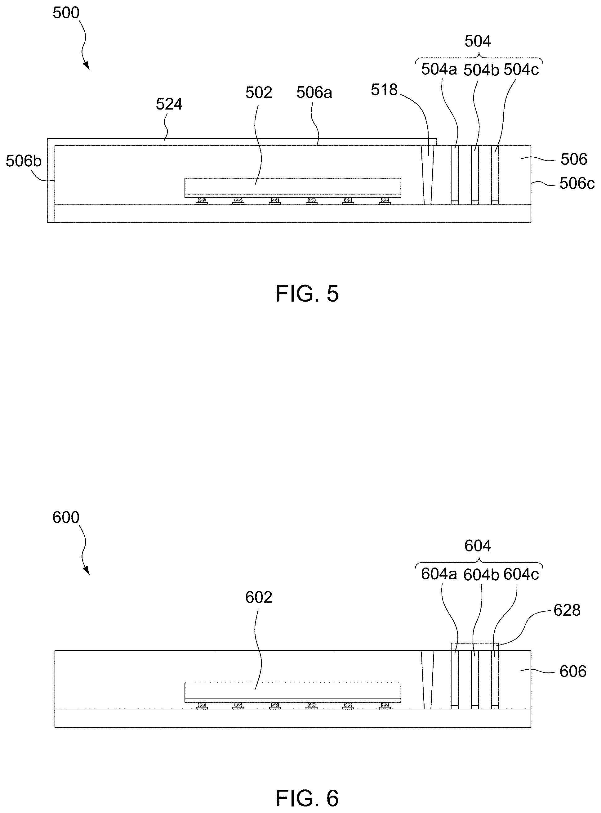
[0055] FIG. 5 illustrates a cross-sectional view of a semiconductor package 500 according to an embodiment of the present disclosure. The semiconductor package 500 in FIG. 5 is similar to the semiconductor package 400 in FIG. 4, with differences including that the conductive layer 524 disposed on the encapsulant 506 covers the top surface 506a of the encapsulant 506, a single one of the side surfaces 506b, 506c of the encapsulant 506, the exposed surface of the third semiconductor component 518, but not the exposed surface of the second semiconductor component 504 (including the feeding element 504b and the shielding elements 504a, 504c).
[0056] FIG. 6 illustrates a cross-sectional view of a semiconductor package 600 according to an embodiment of the present disclosure. The semiconductor package 600 in FIG. 6 is similar to the semiconductor package 300 in FIG. 3(a), with differences including that the semiconductor package 600 includes a connector 628 disposed on the encapsulant 606. The connector 628 is disposed adjacent to the second semiconductor component 604. In the embodiment illustrated in FIG. 6, the connector 628 is disposed on the feeding element 604b and the shielding element 604a, 604c. The connector 628 may be, for example, a connector for connecting to an antenna layer.
[0057] FIG. 7 illustrates a cross-sectional view of a semiconductor package 700 according to an embodiment of the present disclosure. The semiconductor package 700 in FIG. 7 is similar to the semiconductor package 500 in FIG. 5, with differences including that the semiconductor package 700 includes a connector 728 disposed on the encapsulant 706. The connector 728 is disposed adjacent to the second semiconductor component 704. In the embodiment illustrated in FIG. 7, the connector 728 is disposed on the feeding element 704b and the shielding element 704a, 704c. The connector 728 may be, for example, a connector for connecting to an antenna layer.
[0058] FIG. 8 illustrates a cross-sectional view of a semiconductor package 800 according to an embodiment of the present disclosure. The semiconductor package 800 in FIG. 8 is similar to the semiconductor package 700 in FIG. 7, with differences including that the semiconductor package 800 includes an antenna layer 830 disposed adjacent to the feeding element 804b and the shielding elements 804a, 804c and electrically connected to the feeding element 804b and the shielding element 804a, 804c. In the embodiment illustrated in FIG. 8, the antenna layer 830 includes a second connector 832 connecting to the first connector 828 disposed on the feeding element 804b and the shielding elements 804a, 804c.
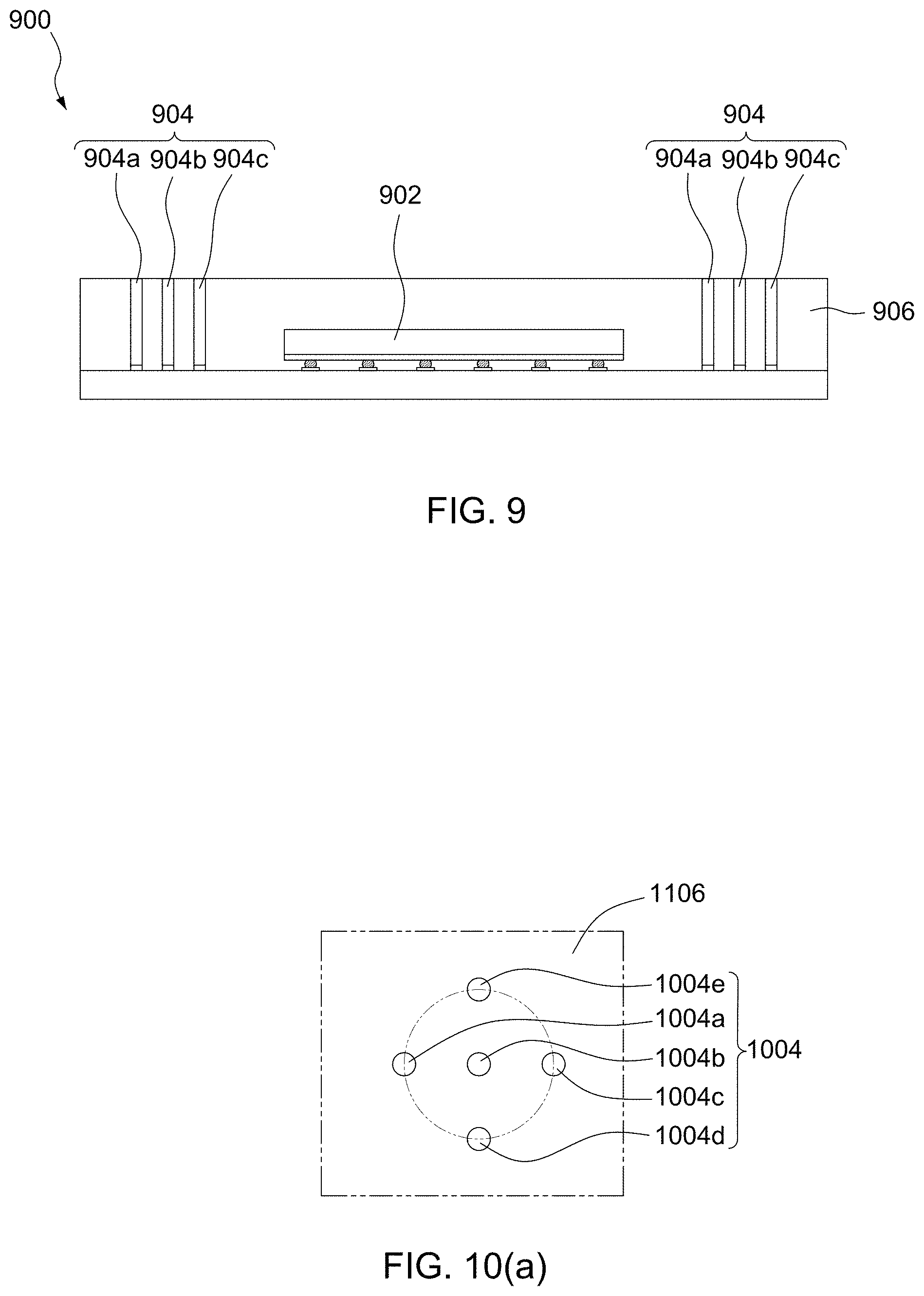
[0059] FIG. 9 illustrates a cross-sectional view of a semiconductor package 900 according to an embodiment of the present disclosure. The semiconductor package 900 in FIG. 9 is similar to the semiconductor package 100 in FIG. 1(a), with differences including that the semiconductor package 900 includes a third semiconductor component 934 disposed on the substrate 908 and the encapsulant 906 exposes the second semiconductor component 904 and the third semiconductor component 934. The third semiconductor component 934 is disposed on the first surface 901a of the substrate 901 and may be at the same side or opposite side of the second semiconductor component 904. The third semiconductor component 934 may be any semiconductor component including, for example, a RF structure, a chip, a package, an interposer, or a combination thereof. The third semiconductor component 934 may be the same or different from the second semiconductor component 904. In the embodiment illustrated in FIG. 9, the third semiconductor component 934 is a RF structure including includes at least one preformed feeding element 934b and at least one preformed shielding element 934a, 934c and disposed at the opposite side of the second semiconductor component 904.
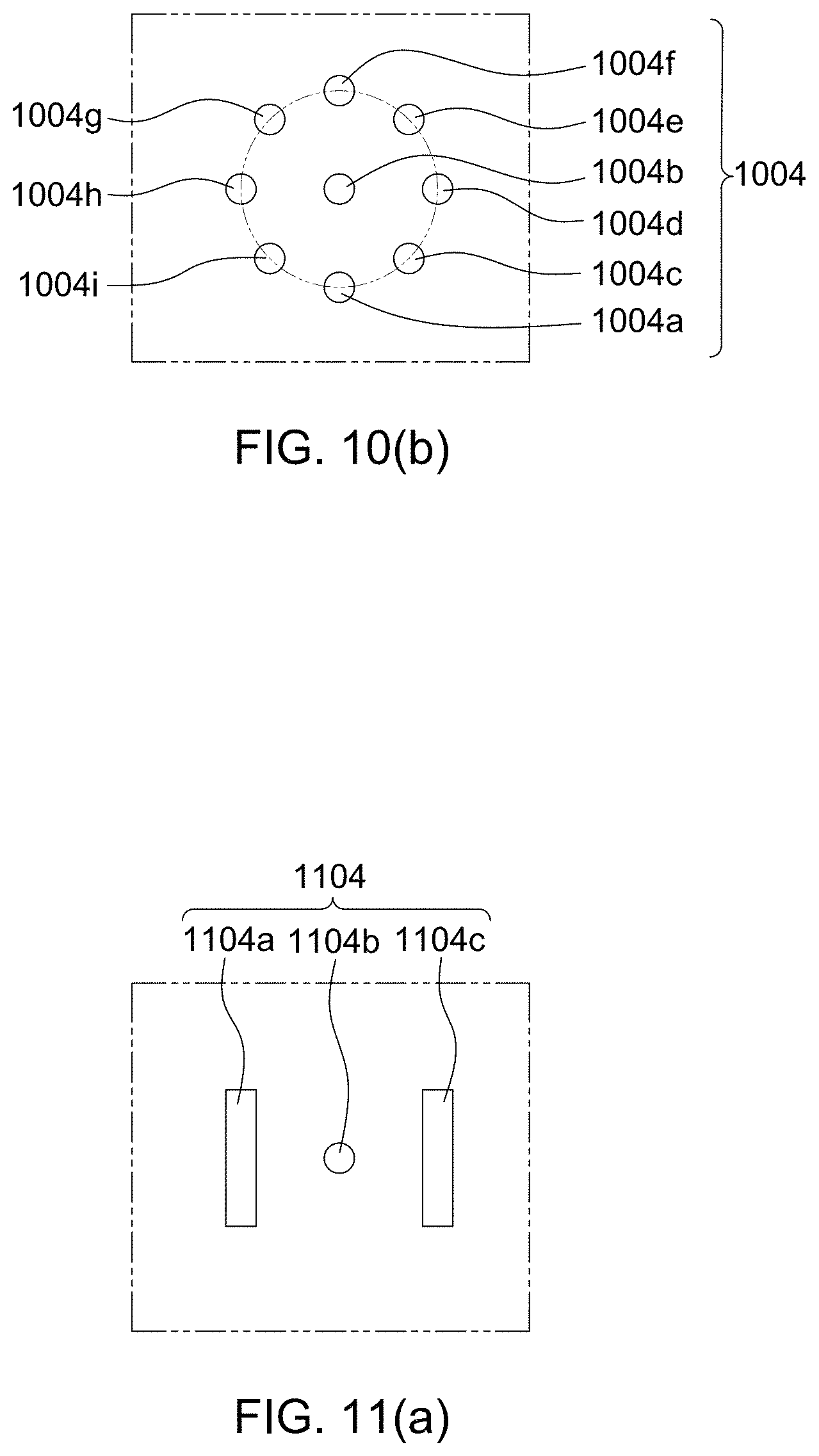
[0060] FIG. 10(a) illustrates a top view of a second semiconductor component in accordance with embodiments of the present disclosure. The second semiconductor component 1004 comprises one feeding element 1004b and four pieces of shielding element 1004a, 1004c, 1004d, 1004e. The four pieces of shielding element 1004a, 1004c, 1004d, 1004e are disposed adjacent to the feeding element 1004b. The four pieces of shielding element 1004a, 1004c, 1004d, 1004e surround the feeding element 1004b. The shielding element 1004a, 1004c, 1004d, 1004e includes an opening between each pieces 1004a, 1004c, 1004d, 1004e. The four pieces of shielding element 1004a, 1004c, 1004d, 1004e are spaced apart from each other by the encapsulant 1006. The four pieces of shielding element 1004a, 1004c, 1004d, 1004e may surround the feeding element 1004b in any arrangement, for example, in a square-like, round-like, rectangular-like, trapezoidal-like, oval-like, rhombic-like, or parallelogram-like arrangement. In the embodiment illustrated in FIG. 10(a), the four pieces of shielding element 1004a, 1004c, 1004d, 1004e surround the feeding element 1004b in a round-like arrangement.
[0061] FIG. 10(b) illustrates a top view of a second semiconductor component in accordance with embodiments of the present disclosure. The second semiconductor component 1005 in FIG. 10(b) is similar to the second semiconductor component 1004 in FIG. 10(a), with differences including that the second semiconductor component 1005 includes eight pieces of shielding element 1004a, 1004c, 1004d, 1004e, 1004f, 1004g, 1004h, 1004i disposed adjacent to the feeding element 1004b. The eight pieces of shielding element 1004a, 1004c, 1004d, 1004e, 1004f, 1004g, 1004h, 1004i surround the feeding element 1004b in a round-like arrangement.
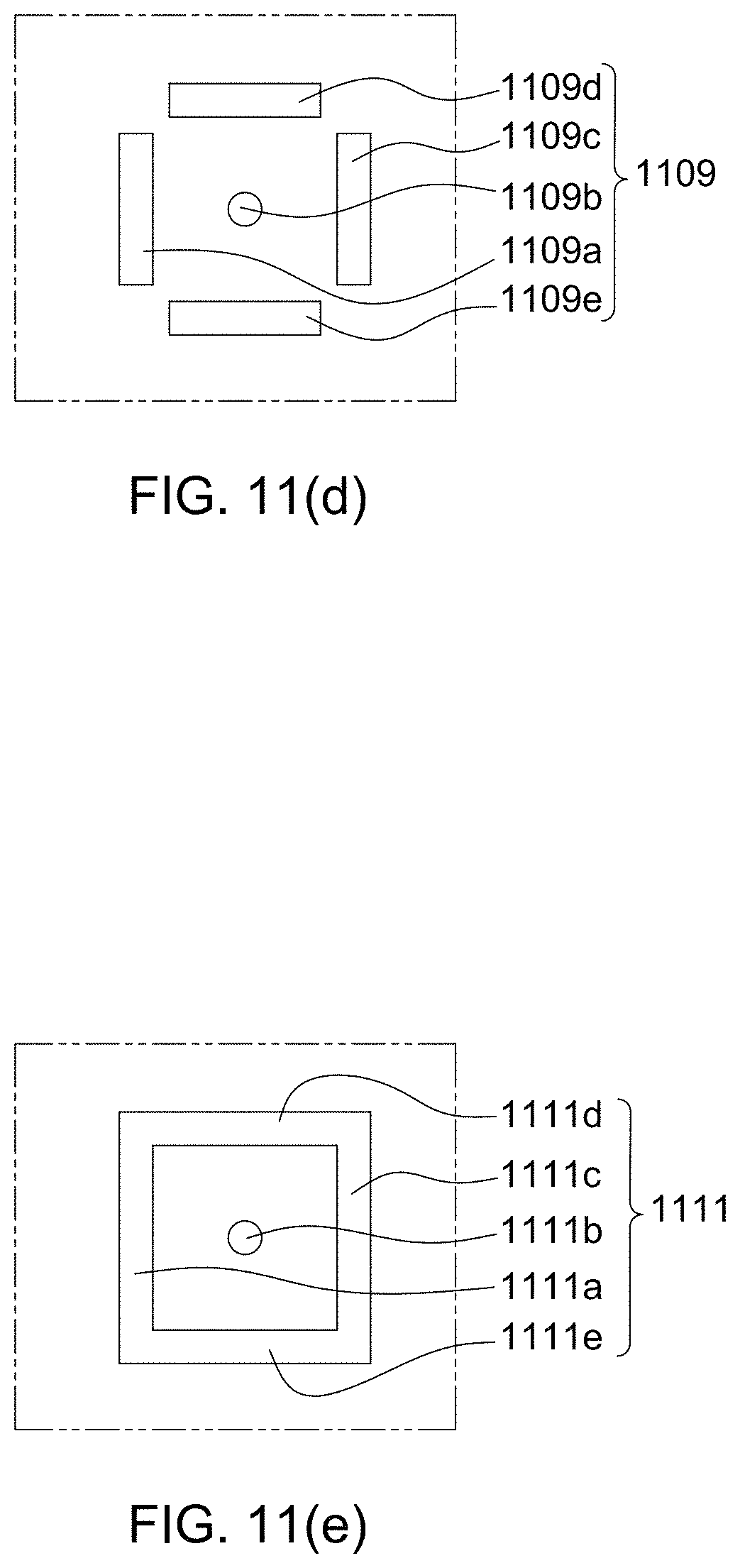
[0062] FIG. 11(a) illustrates a top view of a second semiconductor component in accordance with embodiments of the present disclosure. The second semiconductor component 1104 in FIG. 11(a) is similar to the second semiconductor component 104 in FIG. 1(b), with differences including that the shielding element 1104a, 1104c are preformed in a rectangular-like column shape.
[0063] FIG. 11(b) illustrates a top view of a second semiconductor component in accordance with embodiments of the present disclosure. The second semiconductor component 1105 in FIG. 11(b) is similar to the second semiconductor component 1104 in FIG. 11(a), with differences including that the second semiconductor component 1105 includes three pieces of shielding element 1105a, 1105c, 1105d disposed adjacent to the feeding element 1105b. The three pieces of shielding element 1105a, 1105c, 1105d surround the feeding element 1105b. The three pieces of shielding element 1105a, 1105c, 1105d may surround about 3/4 of the surroundings of the feeding element 1105b.
[0064] FIG. 11(c) illustrates a top view of a second semiconductor component in accordance with embodiments of the present disclosure. The second semiconductor component 1107 in FIG. 11(c) is similar to the second semiconductor component 1105 in FIG. 11(b), with differences including that the three pieces of shielding element 1107a, 1107c, 1107d contact each other and there is no opening between each of them.
[0065] FIG. 11(d) illustrates a top view of a second semiconductor component in accordance with embodiments of the present disclosure. The second semiconductor component 1109 in FIG. 11(c) is similar to the second semiconductor component 1105 in FIG. 11(b), with differences including that there are four pieces of shielding element 1109a, 1109c, 1109d, 1109e surround the feeding element 1109b. The four pieces of shielding element four pieces of shielding element 1109a, 1109c, 1109d, 1109e surround the feeding element 1109b in a square-like arrangement.
[0066] FIG. 11(e) illustrates a top view of a second semiconductor component in accordance with embodiments of the present disclosure. The second semiconductor component 1111 in FIG. 11(e) is similar to the second semiconductor component 1109 in FIG. 11(d), with differences including that the four pieces of shielding element 1111a, 1111c, 1111d, 1111e contact each other and there is no opening between each of them.
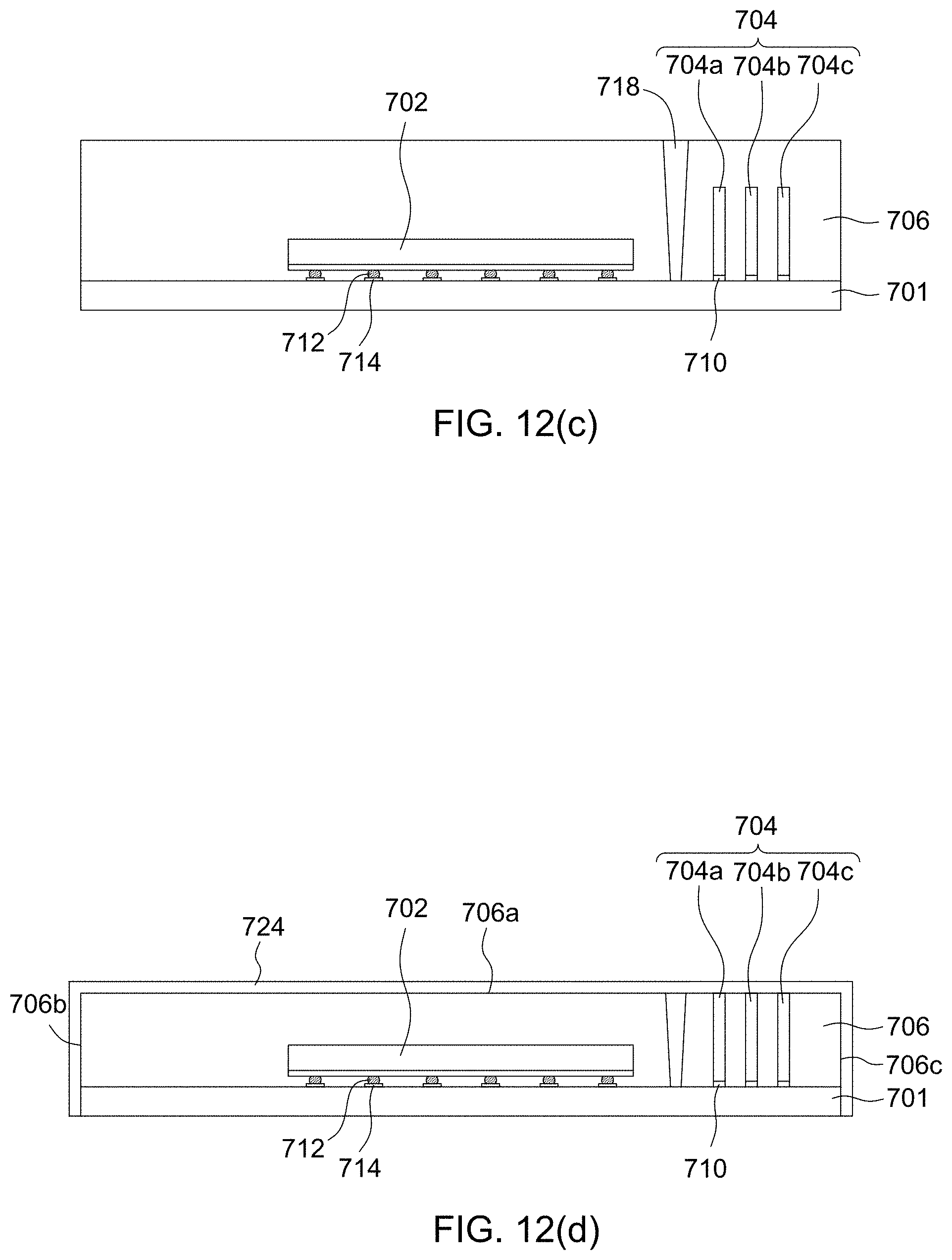
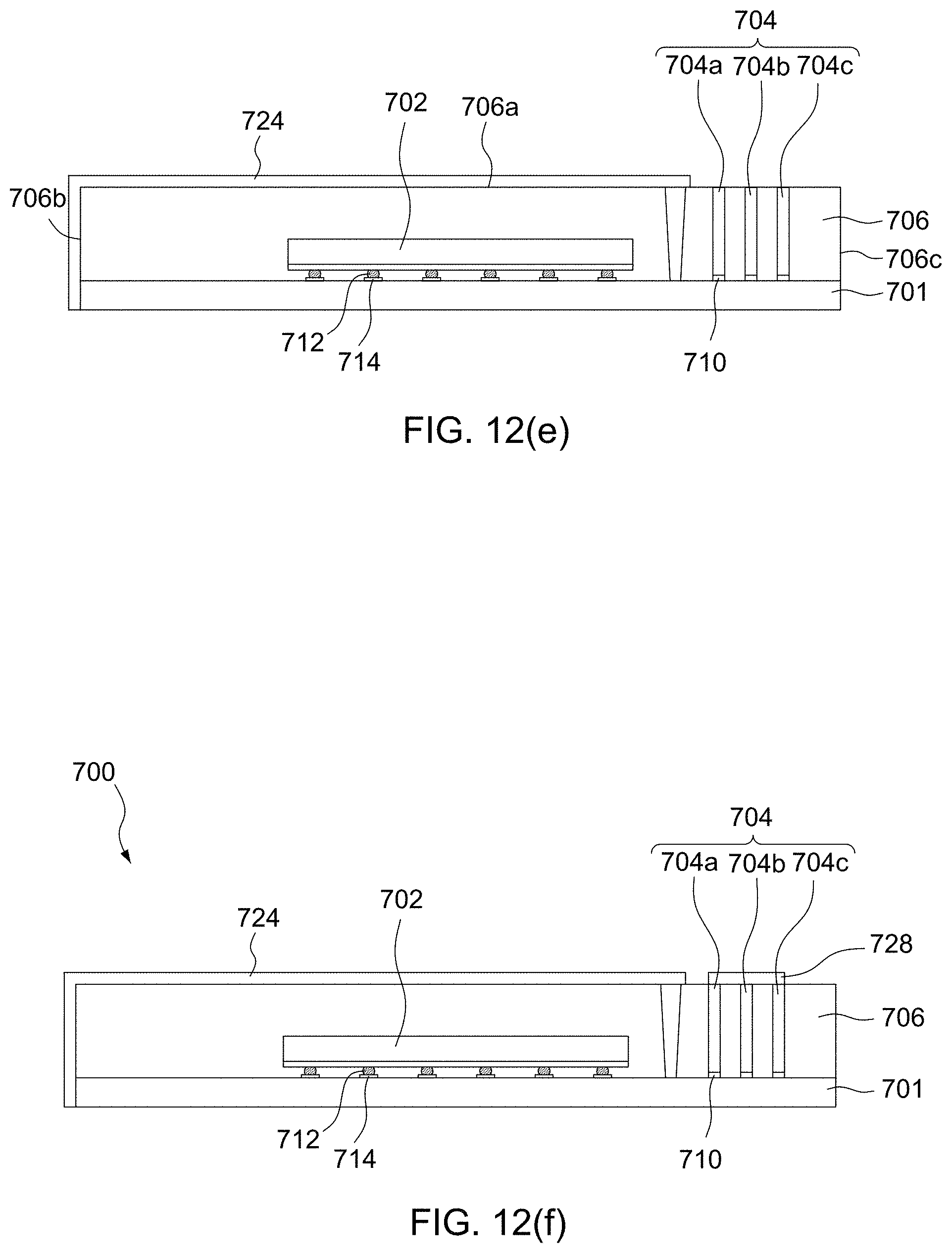
[0067] FIGS. 12(a)-12(b) illustrate a method for manufacturing a semiconductor package such as the semiconductor package 100 of FIG. 1(a). FIGS. 12(a)-12(c) illustrate a method for manufacturing a semiconductor package such as the semiconductor package 300 of FIG. 3(a). FIGS. 12(a)-12(d) illustrate a method for manufacturing a semiconductor package such as the semiconductor package 400 of FIG. 4. FIGS. 12(a)-12(e) illustrate a method for manufacturing a semiconductor package such as the semiconductor package 500 of FIG. 5. FIGS. 12(a)-12(f) illustrate a method for manufacturing a semiconductor package such as the semiconductor package 700 of FIG. 7.
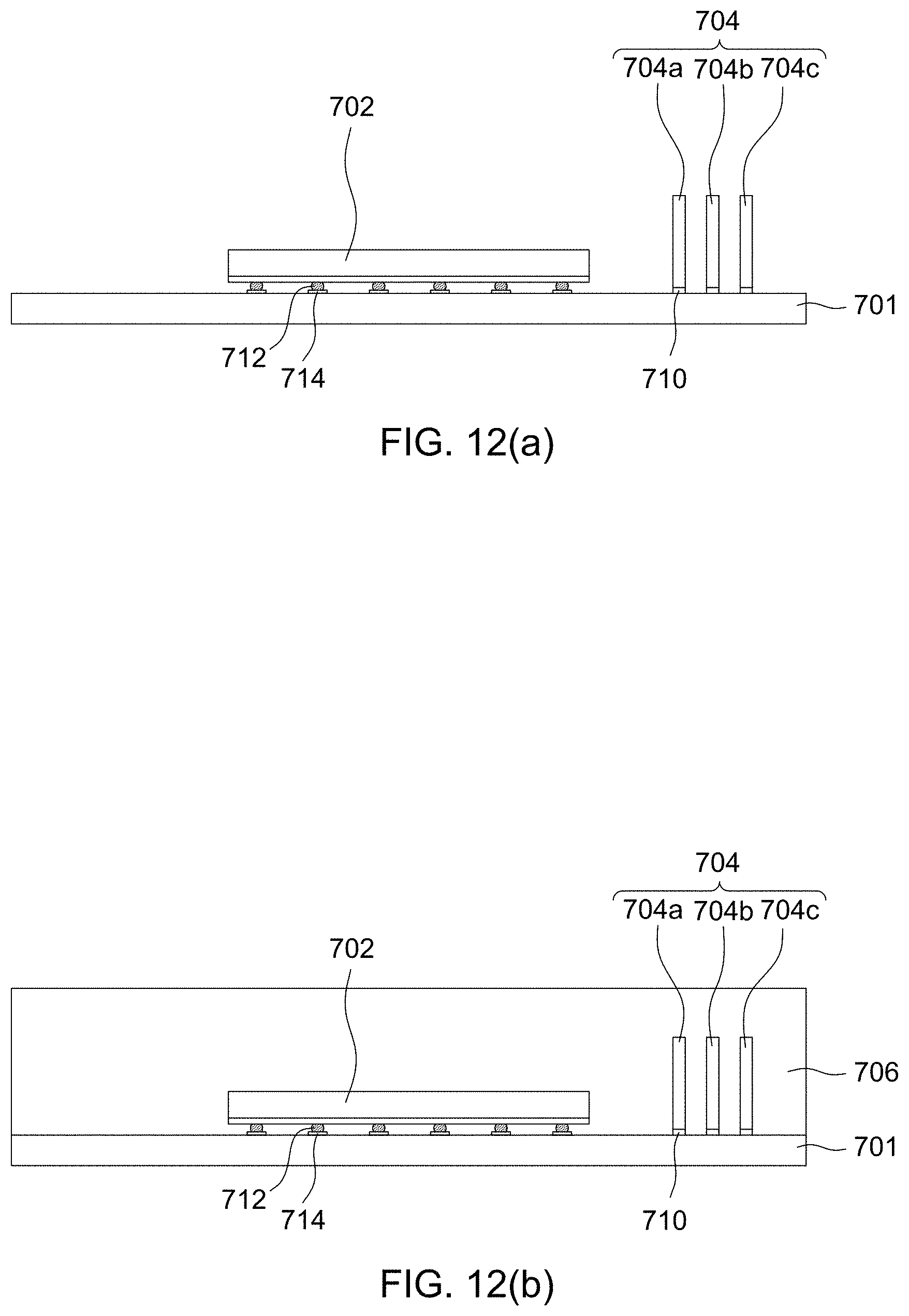
[0068] Referring to FIG. 12(a), a first semiconductor component 702 and a second semiconductor component 704 are provided on a substrate 701. The first semiconductor component 702 is a chip including at least one conductive connector 712. The second semiconductor component 704 is a RF structure including at least one feeding element 704b and at least one shielding element 704a, 704c. The substrate 701 includes at least one bonding pad 714. The shielding element comprises two pieces 704a, 704c. The feeding element 704b and the shielding element 704a, 704c were preformed in a round-like column shape by a molding technology before being provided on the substrate 701. The preformed feeding element 704b and the preformed shielding element 704c are disposed on the substrate 701 by a surface mounted technology (SMT). The temperature of the SMT process is preferably controlled below about 200.degree. C. The working temperature of the solder paste 710 is preferably below about 200.degree. C. in the SMT process.
[0069] Referring to FIG. 12(b), an encapsulant 706 is disposed between the first semiconductor component 702 and the second semiconductor component 704 by, for example, molding. The encapsulant 706 encapsulates the first semiconductor component 702, the preformed feeding element 704b and the preformed shielding element 704a, 704c. The encapsulant 706 covers the first semiconductor component 702, the preformed feeding element 704b and the preformed shielding element 704a, 704c, surrounds the preformed feeding element 704b and the preformed shielding element 704a, 704c, and extends from the preformed shielding element 704a to the first semiconductor component 702. The encapsulant 706 may be, for example, a solder mask (the material of which is, for example, polyimide (PI)) or a passivation layer (the material of which is, for example, a metal oxide) or an underfill. The encapsulant 706 may include a filler, the material of which is, for example, silica and/or carbon.
[0070] Referring to FIG. 12(c), a third semiconductor component 718 is disposed in the encapsulant 706. The third semiconductor component 718 is disposed between the first semiconductor component 702 and the second semiconductor component 704. The third semiconductor component 718 may be, for example, a compartment separating the first semiconductor component 702 from the second semiconductor component 704, or a conductive via. The encapsulant 706 defines the location for forming the compartment or the conductive via. The compartment or conductive via may be formed by drilling (or etching) and electroplating. Accordingly, as described above for the encapsulant 706 including fillers adjacent to the compartment or conductive via 718, they cannot remain intact in shape as they are damaged by the drilling or etching process and therefore their effects in the encapsulant 706 as fillers will be deteriorated.
[0071] Referring to FIG. 12(d), the encapsulant 706 is ground to expose the second semiconductor component 704. Subsequently, a separation technique (e.g., sawing) is performed to obtain individual semiconductor packages such as the semiconductor package 300 of FIG. 3(a). A conductive layer 724 is disposed on the encapsulant 706 by, for example, a electroplating technology where it covers the top surface 706a of the encapsulant 706, the side surfaces 706b, 706c of the encapsulant 706, the exposed surface of the second semiconductor component 704 (including the feeding element 704b and the shielding elements 704a, 704c), and the exposed surface of the third semiconductor component 718. The conductive layer 724 may be, for example, a shielding layer or a conformal shielding layer.
[0072] Referring to FIG. 12(e), the conductive layer 724 is disposed on the encapsulant 706 where it selectively covers the top surface 706a of the encapsulant 706, one of the side surfaces 706b, 706c of the encapsulant 706, the exposed surface of the third semiconductor component 718 except for the exposed surface of the second semiconductor component 704. The conductive layer 724 may be, for example, a shielding layer or a conformal shielding layer, and be formed by photolithography in combination with etching and electroplating or physical vapor deposition.
[0073] Referring to FIG. 12(f), a connector 728 is disposed on the encapsulant 706. The connector 728 is disposed adjacent to the second semiconductor component 704. In the embodiment illustrated in FIG. 7, the connector 728 is disposed on the feeding element 704b and the shielding elements 704a, 704c. The connector 728 may be, for example, a connector for connecting to an antenna layer. The connector 728 may be formed by photolithography in combination with etching and electroplating or physical vapor deposition.
[0074] As used herein and not otherwise defined, the term "about" are used to describe and account for small variations. When used in conjunction with an event or circumstance, the term can encompass instances in which the event or circumstance occurs precisely as well as instances in which the event or circumstance occurs to a close approximation. For example, when used in conjunction with a numerical value, the term can encompass a range of variation of less than or equal to +10% of that numerical value, such as less than or equal to +5%, less than or equal to +4%, less than or equal to +3%, less than or equal to +2%, less than or equal to +1%, less than or equal to +0.5%, less than or equal to +0.1%, or less than or equal to +0.05%.
[0075] While the present disclosure has been described and illustrated with reference to specific embodiments thereof, these descriptions and illustrations are not limiting. It should be understood by those skilled in the art that various changes may be made and equivalents may be substituted without departing from the true spirit and scope of the present disclosure as defined by the appended claims. The illustrations may not necessarily be drawn to scale. There may be distinctions between the artistic renditions in the present disclosure and the actual apparatus due to manufacturing processes and tolerances. There may be other embodiments of the present disclosure which are not specifically illustrated. The specification and the drawings are to be regarded as illustrative rather than restrictive. Modifications may be made to adapt a particular situation, material, composition of matter, method, or process to the objective, spirit and scope of the present disclosure. All such modifications are intended to be within the scope of the claims appended hereto. While the methods disclosed herein have been described with reference to particular operations performed in a particular order, it will be understood that these operations may be combined, sub-divided, or re-ordered to form an equivalent method without departing from the teachings of the present disclosure. Accordingly, unless specifically indicated herein, the order and grouping of the operations are not limitations.
* * * * *
D00000
D00001
D00002
D00003
D00004
D00005
D00006
D00007
D00008
D00009
D00010
D00011
D00012
D00013
XML
uspto.report is an independent third-party trademark research tool that is not affiliated, endorsed, or sponsored by the United States Patent and Trademark Office (USPTO) or any other governmental organization. The information provided by uspto.report is based on publicly available data at the time of writing and is intended for informational purposes only.
While we strive to provide accurate and up-to-date information, we do not guarantee the accuracy, completeness, reliability, or suitability of the information displayed on this site. The use of this site is at your own risk. Any reliance you place on such information is therefore strictly at your own risk.
All official trademark data, including owner information, should be verified by visiting the official USPTO website at www.uspto.gov. This site is not intended to replace professional legal advice and should not be used as a substitute for consulting with a legal professional who is knowledgeable about trademark law.