Coiled Capacitor
Kind Code
U.S. patent application number 16/854031 was filed with the patent office on 2020-08-06 for coiled capacitor. The applicant listed for this patent is CAPACITOR SCIENCES INCORPORATED. Invention is credited to Paul FURUTA, Pavel Ivan LAZAREV, Matthew R. ROBINSON.
| Application Number | 20200251281 16/854031 |
| Document ID | 20200251281 / US20200251281 |
| Family ID | 1000004777872 |
| Filed Date | 2020-08-06 |
| Patent Application | download [pdf] |


View All Diagrams
| United States Patent Application | 20200251281 |
| Kind Code | A1 |
| ROBINSON; Matthew R. ; et al. | August 6, 2020 |
COILED CAPACITOR
Abstract
The present disclosure provides a coiled capacitor comprising a coil formed by a flexible multilayered tape, and a first terminating electrode and a second terminating electrode which are located on butts of the coil. The flexible multilayered tape contains the following sequence of layers: first metal layer, a layer of a plastic, second metal layer, a layer of energy storage material. The first metal layer forms ohmic contact with the first terminating electrode and the second metal layer forms ohmic contact with the second terminating electrode. The energy storage material comprises material selected from the list comprising rylene fragments, doped oligoaniline and p-oligo-phenylene, supramolecular structures, colloidal composite with dispersion (suspension) of electro-conductive anisometric particles in an insulator matrix, material comprises a surfactant.
| Inventors: | ROBINSON; Matthew R.; (San Francisco, CA) ; FURUTA; Paul; (Sunnyvale, CA) ; LAZAREV; Pavel Ivan; (Palo Alto, CA) | ||||||||||
| Applicant: |
|
||||||||||
|---|---|---|---|---|---|---|---|---|---|---|---|
| Family ID: | 1000004777872 | ||||||||||
| Appl. No.: | 16/854031 | ||||||||||
| Filed: | April 21, 2020 |
Related U.S. Patent Documents
| Application Number | Filing Date | Patent Number | ||
|---|---|---|---|---|
| 15943342 | Apr 2, 2018 | 10672561 | ||
| 16854031 | ||||
| 14752600 | Jun 26, 2015 | 9941051 | ||
| 15943342 | ||||
| Current U.S. Class: | 1/1 |
| Current CPC Class: | H01G 4/32 20130101; H01G 4/228 20130101; Y02T 10/70 20130101; H01G 4/18 20130101; H01G 4/015 20130101; H01G 4/012 20130101 |
| International Class: | H01G 4/18 20060101 H01G004/18; H01G 4/012 20060101 H01G004/012; H01G 4/232 20060101 H01G004/232; H01G 4/015 20060101 H01G004/015; H01G 4/32 20060101 H01G004/32 |
Claims
1. A coiled capacitor comprising a coil formed by a flexible multilayered tape, and a first terminating electrode and a second terminating electrode which are located on butts of the coil, wherein the flexible multilayered tape contains the following sequence of layers: first metal layer, a layer of a plastic, second metal layer, a layer of energy storage material, wherein the first metal layer forms ohmic contact with the first terminating electrode and the second metal layer forms ohmic contact with the second terminating electrode, and wherein the energy storage material comprises rylene fragments.
2. A coiled capacitor according to claim 1 further comprising a dielectric core around which the flexible multilayered tape is coiled.
3. A coiled capacitor according to claim 1, wherein the rylene fragments include one or more structures selected from the list comprising structures 1-21: ##STR00063## ##STR00064## ##STR00065##
4.-13. (canceled)
14. A coiled capacitor according to claim 1, wherein the energy storage material comprises a ceramic slurry, a sputtered thin film, or a molecularly ordered crystal.
15. A coiled capacitor according to claim 1, wherein the plastic is selected from the list comprising polypropylene (PP), polyethylene terephthalate (PET), polyphenylene sulfide (PPS), polyethylene naphthalate (PEN), polycarbonate (PP), polystyrene (PS), and polytetrafluoroethylene (PTFE) and a thickness of the plastic layer cannot be less than 2 .mu.m.
16.-23. (canceled)
Description
CLAIM OF PRIORITY
[0001] This application is a continuation of U.S. patent application Ser. No. 14/752,600 filed Jun. 26, 2015, the entire contents of which are incorporated herein by reference.
BACKGROUND
[0002] Capacitors with high volumetric energy density, high operating temperature, low equivalent series resistance (ESR), and long lifetime are critical components for pulse-power, automotive, and industrial electronics. The physical characteristics of the dielectric material in the capacitor are the primary determining factors for the performance of a capacitor. Accordingly, improvements in one or more of the physical properties of the dielectric material in a capacitor can result in corresponding performance improvements in the capacitor component, usually resulting in performance and lifetime enhancements of the electronics system or product in which it is embedded. Since improvements in capacitor dielectric can directly influence product size, product reliability, and product efficiency, there is a high value associated with such improvements.
[0003] Certain improvements in capacitor dielectric materials can be considered as enabling to a particular technology application. For example, capacitors with high permittivity, high dielectric strength, low ESR, and low dielectric dissipation factor will allow high frequency or pulse-power applications to be reduced to a practical size. High temperature operation will greatly simplify next-generation electric vehicles. Improved dielectrics will enable the specific power and reliability of switching power supplies, power conditioners, and filters to be increased. Improved energy density will decrease the area presently devoted to capacitor devices on printed circuit boards, reducing the weight and size of power conditioning systems, power supplies and down-hole tools for use in oil or gas wells.
[0004] To reduce the size of a capacitor while retaining all other physical and electrical characteristics, either an increase in the capacitor dielectric constant or dielectric breakdown strength is necessary. Both are fulfilled with the development of new thin, flexible dielectrics having high voltage breakdown strength, a high dielectric constant and a low ESR loss. Some applications additionally require a stable dielectric constant with no reduction in lifetime at temperatures exceeding 150[deg.] C.
[0005] High voltage non-polar capacitors are conventionally made using a metalized polymer film that is wound into a cylindrical shape. In conventional wound capacitors, the dielectric material is typically a polymer film. Common polymer dielectric materials include polycarbonate, polyethylene terephthalate (PET, also known as polyester), polypropylene, polystyrene, and polysulfone. Polymer dielectric-based foil capacitors are generally fabricated by placing alternating sheets of polymer and metal foil in a stack and rolling the stack into a tubular shape or depositing a metal film on one side of the polymer then rolling two stacked metalized polymer films into a tubular shape. Electrical wires are connected to each metal foil. The dielectric material exists in the form of self-supporting layers that are thick enough to sustain the necessary operating voltage (typically at least 3-6 micrometers). Unfortunately, the large thickness of the polymer sheets reduces the energy storage density. Usually the dielectric constant of these capacitors changes and the lifetime is shortened at temperatures in excess of 100-150.degree. C. due to deficiencies in the polymer material. Alternately, two polymer films coated with a thin layer of metal (usually 17-100 nanometers thick) are wound into a tubular shape to form a capacitor. The thin metal film has the advantage of clearing any short that may form if the polymer dielectric breaks down during operation. This may extend the life of the capacitor and minimize the chances of catastrophic failure of the capacitor. Conventional film capacitors do not have high energy density because the relative permittivity (also known as dielectric constant .kappa.) of the film is relatively low, e.g., less than about 5.
[0006] Amorphous SiO2, HfO2, other metal oxides and stacks of amorphous oxides and nitrides, e.g. SiO2/Si3N4, are disclosed in prior art as dielectric materials of capacitors. A flexible substrate comprised of an insulating polymer film coated with thin metal layers on both sides of the film and a process to deposit the amorphous oxides and oxide/nitride layers on the film to produce a material that can be rolled into cylindrical shapes is also disclosed in prior art.
[0007] In the prior art the metallized film capacitors are known. These capacitors include two tightly wound sheets, wrapped around a core. Each sheet includes a dielectric layer and a metallized layer. The metallized layer does not extend to the opposing ends of the sheet leaving a non-metallized margin on opposing sides of each sheet. The ends of the roll formed from the two tightly wound sheets are sprayed with a conductive metal to form a conducting termination for the capacitor. Capacitors made in this way can be used for a variety of purposes depending upon factors such as the type of sheet material as well as the thickness and dielectric constant of the sheet. Typical materials for the sheet are, for example, oriented polypropylene or poly-(ethylene)-terephtalate. The conductive metal termination is typically applied in a vacuum metallizer and is generally comprised of aluminum, zinc or alloys thereof.
SUMMARY
[0008] The present disclosure provides a coiled capacitor which may solve a problem of the further increase of volumetric and mass density of reserved energy associated with some energy storage devices, and at the same time reduce cost of materials.
[0009] Aspects of the present disclosure include use of materials engineered to obtain 1) high permittivity, 2) high dielectric strength (also known as breakdown field E.sub.BD) allowing high voltage, and 3) low amount of carrier substrate.
[0010] In an aspect, the present invention provides a coiled capacitor comprising a coil formed by a flexible multilayered tape, and a first terminating electrode (a first contact layer) and a second terminating electrode (a second contact layer) which are located on butts of the coil. The flexible multilayered tape contains the following sequence of layers: first metal layer, a layer of a plastic, second metal layer, a layer of energy storage material. The first metal layer forms an ohmic contact with the first terminating electrode (the first contact layer) and the second metal layer (the second contact layer) forms an ohmic contact with the second terminating electrode.
INCORPORATION BY REFERENCE
[0011] All publications, patents, and patent applications mentioned in this specification are herein incorporated by reference to the same extent as if each individual publication, patent, or patent application was specifically and individually indicated to be incorporated by reference.
BRIEF DESCRIPTION OF THE DRAWINGS
[0012] FIGS. 1a, 1b and 1c schematically show formation of sets of metal strips on top and bottom surfaces of the plastic layer.
[0013] FIG. 2 shows a formation of the layer of the energy storage material on one of metalized surfaces of the plastic layer.
[0014] FIG. 3 shows a slitting of the intermediate product onto the multilayered tapes.
[0015] FIG. 4 shows a winding of the multilayered tape.
[0016] FIG. 5 shows a formation of the first terminating electrode and a second terminating electrode.
[0017] FIG. 6 shows a formation of two metal strips on top and bottom surfaces of the plastic layer according to the second embodiment.
[0018] FIG. 7 shows a formation of the layer of the energy storage material.
[0019] FIG. 8 shows a winding of the multilayered tape.
[0020] FIG. 9 shows a formation of the first terminating electrode and a second terminating electrode.
DETAILED DESCRIPTION
[0021] While various aspects of the present disclosure are shown and described herein, it will be obvious to those skilled in the art that such aspects are provided by way of example only. Numerous variations, changes, and substitutions may occur to those skilled in the art without departing from the invention. It should be understood that various alternatives to the aspects described herein may be employed.
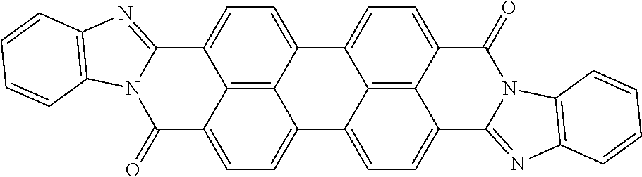
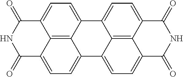
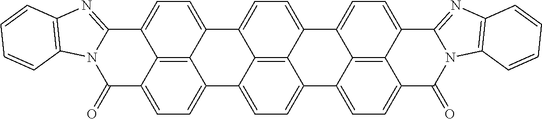
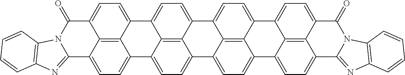
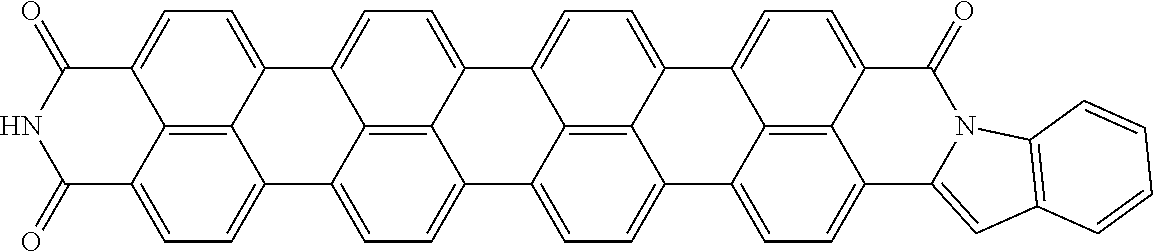
[0022] The present disclosure provides a coiled capacitor. According to one aspect of the present disclosure, the coiled capacitor further comprises a dielectric core around which the flexible multilayered tape is coiled. The energy storage material may be characterized by a dielectric constant .kappa. greater than about 100 and a breakdown field E.sub.bd about greater than or equal to about 0.001 volts (V)/nanometer (nm). The dielectric constant .kappa. may be greater than or equal to about 100, 200, 300, 400, 500, 1000, 2000, 3000, 4000, 5000, 6000, 7000, 8000, 9000, 10,000, or 100,000. The breakdown field may be greater than about 0.01 V/nm, 0.05 V/nm, 0.1 V/nm, 0.2 V/nm, 0.3 V/nm, 0.4 V/nm, 0.5 V/nm, 1 V/nm, or 10 V/nm. By way of example, and not by way of limitation, the energy storage material may be characterized by a dielectric constant .kappa. between about 100 and about 1,000,000 and a breakdown field E.sub.bd between about 0.01 V/nm and about 2.0 V/nm. By way of example, and not by way of limitation, the energy storage material may comprise rylene fragments. According to another aspect of the present disclosure, the rylene fragments may be selected from the list comprising structures 1-21 as given in Table 1.
TABLE-US-00001 TABLE 1 Examples of the energy storage material comprising the rylene fragments: ##STR00001## 1 ##STR00002## 2 ##STR00003## 3 ##STR00004## 4 ##STR00005## 5 ##STR00006## 6 ##STR00007## 7 ##STR00008## 8 ##STR00009## 9 ##STR00010## 10 ##STR00011## 11 ##STR00012## 12 ##STR00013## 13 ##STR00014## 14 ##STR00015## 15 ##STR00016## 16 ##STR00017## 17 ##STR00018## 18 ##STR00019## 19 ##STR00020## 20 ##STR00021## 21
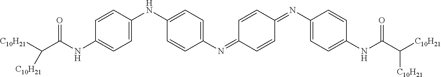
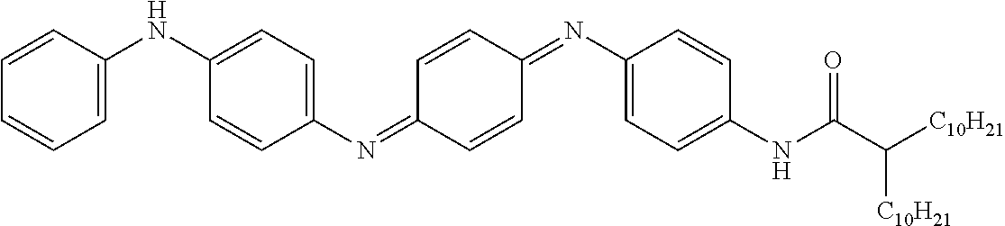
[0023] In one example of a coiled capacitor in accordance with aspects of the present disclosure, the energy storage material is selected from the list comprising doped oligoaniline and p-oligo-phenylene. In another example of a coiled capacitor, the doped oligoaniline is self-doped oligoaniline with SO.sub.3-- groups or COO-- groups on the phenyl rings of aniline. In still another embodiment of the coiled capacitor, the doped oligoaniline is mix-doped by organic structure-inorganic/organic acid mixed to oligoaniline in oxidized state, wherein the organic structure is selected from the list comprising alkyl, aryl and polymers thereof and the inorganic/organic acid is selected from the list comprising SO.sub.3H, COOH, HCl, H.sub.2SO.sub.4, H.sub.3PO.sub.4, HBF.sub.4, HPF.sub.6, benzoic acid and derivatives thereof. According to still another aspect of the present disclosure, the energy storage material may comprise a polymeric material soluble in organic solvents. In yet another embodiment of the present invention, the energy storage material comprises polymers soluble in organic solvents having a structure selected from the structures 22 to 27 as given in Table 2.
TABLE-US-00002 TABLE 2 Examples of the energy storage material comprising the polymers soluble in organic solvents ##STR00022## 22 ##STR00023## 23 ##STR00024## 24 ##STR00025## 25 ##STR00026## 26 ##STR00027## 27
wherein each R.sub.1 and R.sub.2 is independently selected from alkyl, aryl, substituted alkyl, and substituted aryl. In another embodiment of the coiled capacitor, the energy storage material comprises a colloidal composite with a dispersion of electro-conductive anisometric particles in an insulator matrix. In still another example of a coiled capacitor, the electro-conductive anisometric particles comprise an electro-conductive oligomer. In yet another example of the coiled capacitor, the material of the insulator matrix is selected from the group consisting of poly (acrylic acid) (PAA), poly(N-vinylpyrrolidone) (PVP), poly(vinylidene fluoride-hexafluoropropylene) [P(VDF-HFP)], ethylene propylene polymers, which include ethylene propylene rubber (EPR) and ethylene propylene diene monomer (EPDM), and silicone rubber (PDMSO) such as dimethyldicloro siloxane, dimethylsilane diol, and polydimethyl siloxane, polystyrene sulfonic acid (PSS). In one embodiment of the coiled capacitor, the energy storage material comprises a surfactant selected from: dodecylbenzene sulfonate (DBSA), polyoxyethylene glycol alkyl ethers, polyoxypropylene glycol alkyl ethers, polyoxyethylene glycol octylphenol ethers, polyoxyethylene glycol sorbitan alkyl esters, sorbitan alkyl esters, and dobecyldimethylamine oxide.
[0024] In another embodiment of the coiled capacitor, the energy storage material comprises ceramic slurries, sputtered thin films, and molecularly ordered crystals. As used herein the term molecularly ordered crystals refers to films assembled by cascade crystallization or films made from solutions comprising lyotropic liquid crystals. Examples of molecularly ordered crystals include, but are not limited to, energy storage molecular materials that are described, e.g., in U.S. patent application Ser. No. 14/719,072, filed May 21, 2015 (Attorney Docket No. CSI-005), the entire contents of which are incorporated herein by reference. By way of example, and not by way of limitation, a method for making molecularly ordered crystals from a colloidal system with supramolecular complexes may include the following steps: [0025] application of the colloidal system onto a substrate. The colloidal system typically possesses thixotropic properties, which are provided by maintaining a preset temperature and a certain concentration of the dispersed phase; [0026] external alignment upon the system, which can be produced using mechanical factors or by any other means, for example by applying an external electric field at normal or elevated temperature, with or without additional illumination, magnetic field, or optical field (e.g., coherent photovoltaic effect); the degree of the external alignment should be sufficient to impart necessary orientation to the kinetic units of the colloidal system and form a structure, which serves as a base of the crystal lattice of the crystal dielectric layer; and [0027] drying to remove solvents to form the final molecularly ordered crystal.
[0028] In still another example of the coiled capacitor, the plastic is selected from the list comprising polypropylene (PP), polyethylene terephthalate polyester (PET), polyphenylene sulfide (PPS), polyethylene naphthalate (PEN), polycarbonate (PP), polystyrene (PS), and polytetrafluoroethylene (PTFE). In yet another embodiment of the coiled capacitor, the thickness of the plastic layer cannot be less than 2 .mu.m. In still another embodiment of the coiled capacitor, the thickness of the plastic layer varies from 2.5 .mu.m to 52 .mu.m. In one example of the coiled capacitor, the plastic layer comprises polypropylene and the thickness of the plastic layer is equal to 12 .mu.m. In another example of the coiled capacitor, the material of the first metal layer and second metal layer independently selected from the list comprising Pt, Cu, Al, Ag, Au, Ni, and Al:Ni, and the metal foam. In still another example of the coiled capacitor, the thickness of the first and second contact layers independently varies from 10 nm to 1000 nm. In one embodiment of the coiled capacitor, the sheet resistance of the first and second contact layers independently cannot be less than 0.1 Ohm/Square. In another example of the coiled capacitor, the sheet resistance of the first and second contact layers independently varies from 0.1 Ohm/Square to 2.5 Ohm/Square. In yet another example of the coiled capacitor, the metal of the metal foam is selected from the list comprising Al, Ni, Fe, Cu. In one example of the coiled capacitor, the melting temperature of the metal foam is in the range 400 C-700 C. In another example of the coiled capacitor, the metal content in the metal foam for electrode is in the range of 5% up to 30% by weight. In still another example of the coiled capacitor, the metal foam is of closed "bubble" type with maximum conductance per metal content. In yet another example of the coiled capacitor, the size of "bubbles" is in the range of 100 nm up to 100 000 nm. In one example of the coiled capacitor, the material of the first terminating electrode and second terminating electrode independently selected from the list comprising Pt, Cu, Al, Ag, and Au. In another embodiment of the coiled capacitor, the first metal layer is deposited on a portion of a first surface of the plastic layer and this first surface has a first margin portion which is free of deposited metal, and wherein the second metal layer is deposited on a portion of a second surface of the plastic layer and this second surface has a second margin portion which is free of deposited metal and is located on an opposite edge of the plastic layer from the first margin portion.
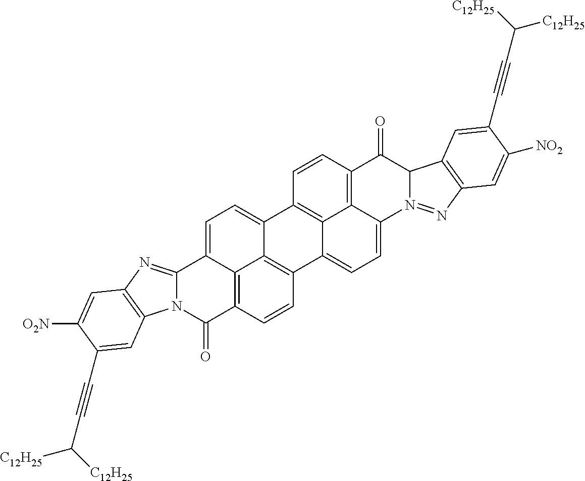
[0029] According to additional aspects of the present disclosure, the energy storage material may include supramolecules or stacks of molecules. Such supramolecules may be formed by self-assembling molecules that stack in rod like molecular structures. Examples of such structures include, but are not limited to, structures selected from the list comprising structures as given in Table 1 and also structures 28-62 as given in Table 3.
TABLE-US-00003 TABLE 3 additional examples of supramolecular structures in the energy storage material ##STR00028## 28 ##STR00029## 29 ##STR00030## 30 ##STR00031## 31 ##STR00032## 32 ##STR00033## 33 ##STR00034## 34 ##STR00035## 35 ##STR00036## 36 ##STR00037## 37 ##STR00038## 38 ##STR00039## 39 ##STR00040## 40 ##STR00041## 41 ##STR00042## 42 ##STR00043## 43 ##STR00044## 44 ##STR00045## 45 ##STR00046## 46 ##STR00047## 47 ##STR00048## 48 ##STR00049## 49 ##STR00050## 50 ##STR00051## 51 ##STR00052## 52 ##STR00053## 53 ##STR00054## 54 ##STR00055## 55 ##STR00056## 56 ##STR00057## 57 ##STR00058## 58 ##STR00059## 59 ##STR00060## 60 ##STR00061## 61 ##STR00062## 62
[0030] To form the energy storage material from such supramolecular structures, organic molecules may be modified using supramolecular chemistry and self-assembled in liquid to form lyotropic liquid crystals. The liquid containing the lyotropic liquid crystals is them coated onto a substrate and the liquid crystals align during coating. Liquid crystals then crystallize to form the energy storage material as the liquid dries.
[0031] In order that the invention may be more readily understood, reference is made to the following examples, which are intended to be illustrative of the invention, but are not intended to be limiting the scope.
EXAMPLES
Example 1
[0032] The example schematically describes a sequence of technological operations for manufacturing of a coiled capacitor in accordance with an aspect of the present disclosure. This example represents one of possible methods of manufacturing of the disclosed coiled capacitor. FIGS. 1a, 1b and 1c show formation of metal strips (1) on top (2, FIG. 1b) and bottom (3, FIG. 1c) surfaces of the plastic layer (4). FIG. 1a shows the metal strips located on the top surface are displaced relatively of the metal strips located on the bottom surface. In this Example the width of the metal strip may vary within the range from 1 cm to 100 cm. The width is not limited by the specified range of values. Generally, the desired width is computed for each application. Various factors can influence size of the width, such as roll size, power, energy, etc. The large influence on the width can render prospective application of the disclosed coiled capacitor. The thickness of the metal strip may vary within the range from 0.01 .mu.m to 1 .mu.m. The distance between strips may change from 0.5 mm to 3 mm. The key feature of this example is the use of one plastic layer as a load-carrying substrate for all layers in the capacitor that are coated onto this plastic layer or supported by this plastic layer.
[0033] Metal strips are formed onto opposite surfaces of the plastic layer so that margin portions which are free of deposited metal have been generated on each surface of the plastic layer and these margin portions are located on an opposite edge of the plastic layer. The following stage is formation of the layer of the energy storage material on one of metalized surfaces of the plastic layer shown in FIG. 2. This formation comprises two steps: first step is application of a solution of the energy storage material and second step comprises a drying the applied solution to form a solid layer of the energy storage material (5). The thickness of the layer of the energy storage material may vary within the range from 0.5 .mu.m to 50 .mu.m. Thus at this stage an intermediate product for the further formation of the coiled capacitor is formed. Then, a slitting of the intermediate product onto the multilayered tapes is made. The schematic view of the received multilayered tape is shown in the FIG. 3. FIG. 3 shows that the first metal layer (6) is deposited on a portion of a first surface of the plastic layer (7) and this first surface has a first margin portion (8) which is free of deposited metal, and wherein the second metal layer (9) is deposited on a portion of a second surface of the plastic layer (7) and this second surface has a second margin portion (10) which is free of deposited metal and is located on an opposite edge of the plastic layer from the first margin portion. Further a winding of the multilayered tape is carried out (see, FIG. 4). Then the first terminating electrode (a first contact layer) (11) and a second terminating electrode (a second contact layer) (12) located on butts of the coil are formed (see, FIG. 5). Finally, a healing is done by applying a precisely calibrated voltage across the first and second terminating electrodes of the coiled capacitor so that any existing defects will be "burned away".
Example 2
[0034] This example schematically describes another sequence of technological operations for manufacturing of the coiled capacitor. FIG. 6 shows formation of two metal strips (13) and (14) on top (15) and bottom (16) surfaces of a plastic layer (17). FIG. 6 shows the metal strip located on the top surface is displaced laterally relative to the metal strip located on the bottom surface. Thus, the first metal strip (13) is deposited on a portion of a first surface of the plastic layer (15) and this first surface has a first margin portion (18) which is free of deposited metal, and wherein the second metal strip (14) is deposited on a portion of a second surface of the plastic layer (16) and this second surface has a second margin portion (19) which is free of deposited metal and is located on an opposite edge of the plastic layer from the first margin portion. The thickness of the plastic layer varies from 2.5 .mu.m to 52 .mu.m. The width of a metal strip may vary within the range from 1 cm to 100 cm and its thickness may vary within the range from 0.01 .mu.m to 1 .mu.m. The plastic layer is used as a load-carrying substrate for all other layers in the capacitor that are coated onto this plastic layer or supported by this plastic layer.
[0035] The following stage is formation of the layer of the energy storage material (20) on one of metalized surfaces of the plastic layer shown in FIG. 7. This formation comprises two steps: first step is application of solution of the energy storage material and second step comprises a drying to form a solid layer of the energy storage material (20). Thickness of the layer of the energy storage material may vary within the range from 0.5 .mu.m to 50 .mu.m. Further a winding of the multilayered tape into a roll is carried out (see, FIG. 8). Then the first terminating electrode (a first contact layer) (21) and a second terminating electrode (a second contact layer) (22) located on butts of the coil are formed (see, FIG. 9). Finally, a healing is done by applying a precisely calibrated voltage across the first and second terminating electrodes of the coiled capacitor so that any existing defects will be "burned away".
[0036] While the above is a complete description of the preferred embodiment of the present invention, it is possible to use various alternatives, modifications and equivalents. Therefore, the scope of the present invention should be determined not with reference to the above description but should, instead, be determined with reference to the appended claims, along with their full scope of equivalents. Any feature described herein, whether preferred or not, may be combined with any other feature described herein, whether preferred or not. In the claims that follow, the indefinite article "A", or "An" refers to a quantity of one or more of the item following the article, except where expressly stated otherwise. As used herein, in a listing of elements in the alternative, the word "or" is used in the logical inclusive sense, e.g., "X or Y" covers X alone, Y alone, or both X and Y together, except where expressly stated otherwise. Two or more elements listed as alternatives may be combined together. The appended claims are not to be interpreted as including means-plus-function limitations, unless such a limitation is explicitly recited in a given claim using the phrase "means for."
* * * * *


D00000

D00001

D00002

D00003

D00004

D00005

D00006

XML
uspto.report is an independent third-party trademark research tool that is not affiliated, endorsed, or sponsored by the United States Patent and Trademark Office (USPTO) or any other governmental organization. The information provided by uspto.report is based on publicly available data at the time of writing and is intended for informational purposes only.
While we strive to provide accurate and up-to-date information, we do not guarantee the accuracy, completeness, reliability, or suitability of the information displayed on this site. The use of this site is at your own risk. Any reliance you place on such information is therefore strictly at your own risk.
All official trademark data, including owner information, should be verified by visiting the official USPTO website at www.uspto.gov. This site is not intended to replace professional legal advice and should not be used as a substitute for consulting with a legal professional who is knowledgeable about trademark law.