Radar Based Fill-Level Sensor
Kind Code
U.S. patent application number 15/774347 was filed with the patent office on 2020-08-06 for radar based fill-level sensor. The applicant listed for this patent is Endress + Hauser SE + Co. KG. Invention is credited to Martin Hitzler, Winfried Mayer, Christian Waldschmidt.
| Application Number | 20200249067 15/774347 |
| Document ID | / |
| Family ID | 1000004800428 |
| Filed Date | 2020-08-06 |
| United States Patent Application | 20200249067 |
| Kind Code | A1 |
| Mayer; Winfried ; et al. | August 6, 2020 |
Radar Based Fill-Level Sensor
Abstract
A radar based, fill-level sensor comprising at least one semiconductor element, including at least a semiconductor chip and a chip package, in which the at least one semiconductor chip is arranged, wherein the at least one semiconductor chip has at least one coupling element, which serves as a signal gate for electromagnetic waves, preferably in the millimeter wave region, characterized in that at least one first resonator structure is arranged on a surface portion of the chip package.
| Inventors: | Mayer; Winfried; (Buch, DE) ; Hitzler; Martin; (Dillingen, DE) ; Waldschmidt; Christian; (Ulm, DE) | ||||||||||
| Applicant: |
|
||||||||||
|---|---|---|---|---|---|---|---|---|---|---|---|
| Family ID: | 1000004800428 | ||||||||||
| Appl. No.: | 15/774347 | ||||||||||
| Filed: | November 3, 2016 | ||||||||||
| PCT Filed: | November 3, 2016 | ||||||||||
| PCT NO: | PCT/EP2016/076562 | ||||||||||
| 371 Date: | May 8, 2018 |
| Current U.S. Class: | 1/1 |
| Current CPC Class: | G01F 23/284 20130101; H01Q 1/2283 20130101; H01L 2223/6677 20130101; H01L 21/4825 20130101; H01P 11/008 20130101; H01Q 1/225 20130101; H01L 23/4952 20130101; H01P 7/10 20130101; H01P 3/16 20130101; H01L 2223/6627 20130101; H01L 23/66 20130101 |
| International Class: | G01F 23/284 20060101 G01F023/284; H01L 21/48 20060101 H01L021/48; H01L 23/495 20060101 H01L023/495; H01L 23/66 20060101 H01L023/66; H01P 7/10 20060101 H01P007/10; H01P 3/16 20060101 H01P003/16; H01P 11/00 20060101 H01P011/00; H01Q 1/22 20060101 H01Q001/22 |
Foreign Application Data
| Date | Code | Application Number |
|---|---|---|
| Nov 13, 2015 | DE | 10 2015 119 690.5 |
Claims
1-13. (canceled)
14. A radar based fill-level sensor, comprising: at least one semiconductor element, including at least a semiconductor chip and a chip package, in which the at least one semiconductor chip is arranged, wherein the at least one semiconductor chip has at least one coupling element, which serves as a signal gate for electromagnetic waves, preferably in the millimeter wave region, characterized in that at least one first resonator structure is arranged on a surface portion of the chip package.
15. The radar based fill-level sensor as claimed in claim 14, wherein: at least one second resonator structure is arranged between said semiconductor chip and said at least one first resonator structure.
16. The radar based fill-level sensor as claimed in claim 14, wherein: said chip package includes on the surface portion, on which said at least one first resonator structure is arranged, a depression extending in the direction of said at least one semiconductor chip.
17. The radar based fill-level sensor as claimed in claim 14, wherein: said chip package includes on the surface portion, on which said at least one first resonator structure is arranged, a depression extending in the direction of said at least one second resonator structure has.
18. The radar based fill-level sensor as claimed in claim 14, wherein: said at least one semiconductor element is arranged on a printed circuit board; and a dielectric lens is secured on said printed circuit board in such a way that said at least one semiconductor element lies in the focal point of said delectric lens.
19. The radar based fill-level sensor as claimed in claim 14, wherein: said dielectric semiconductor element is arranged on a printed circuit board; and at least one hollow conductor is arranged on the printed circuit board transferring the electromagnetic waves produced by said dielectric semiconductor element.
20. The radar based fill-level sensor as claimed in claim 19, further comprising: a dielectric waveguide arranged said the depression, so that electromagnetic waves out-coupled from said coupling element are led by means of a dielectric waveguide into a hollow conductor, which preferably has a terminal structure for in-coupling the electromagnetic waves.
21. A method for manufacturing a radar based fill-level sensor, comprising: a radar based fill-level sensor, at least one semiconductor element, including at least a semiconductor chip and a chip package, in which the at least one semiconductor chip is arranged, wherein the at least one semiconductor chip has at least one coupling element, which serves as a signal gate for electromagnetic waves, preferably in the millimeter wave region, characterized in that at least one first resonator structure is arranged on a surface portion of the chip package. the method comprising the steps as follows: sending radiation through the semiconductor element for determining a position of the semiconductor chip relative to the chip package; partially removing the chip package until a surface portion of the chip package has at least one depression extending in the direction of the at least one coupling element; producing a first resonator structure in the at least one depression, so that the separation between the at least one first resonator structure and the at least one coupling element of the semiconductor chip is lessened.
22. The method as claimed in claim 21, wherein: said producing of the first resonator structure in the at least one depression is performed by means of a 2D- or 3D printing method or an MID method.
23. The method as claimed in claim 21, wherein: said sending of radiation through the semiconductor element is performed by means of x-rays.
24. The method as claimed in claim 21, wherein: said partial removing of the chip package is performed by means of milling or laser beam machining.
25. The method as claimed in claim 21, wherein: the first resonator structure comprises a rectangular metal platelet; and an edge length of the first resonator structure corresponds to a half wavelength or an integer multiple half wavelength of the electromagnetic waves.
26. The method as claimed in claim 21, wherein: the first resonator structure is embodied as a dielectric resonator structure preferably of quartz glass, ceramic, plastic or as a structured substrate platelet.
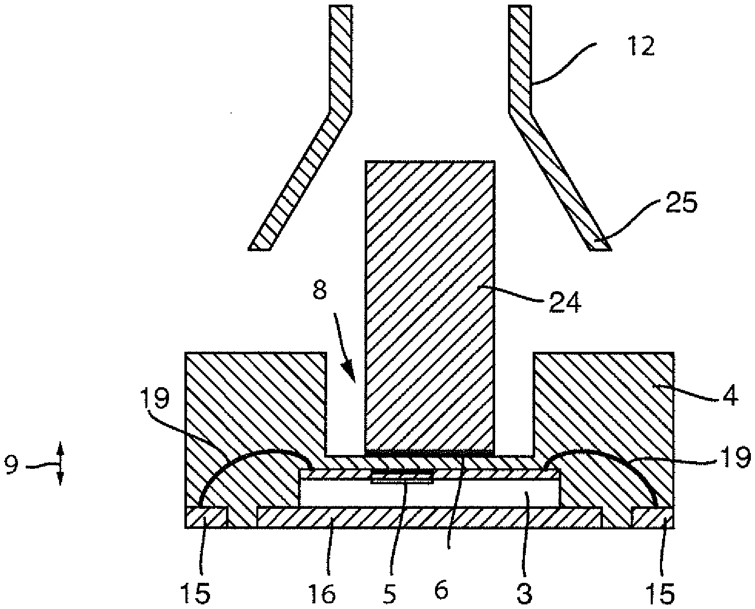
Description
[0001] The invention relates to a radar based, fill-level sensor having at least one semiconductor element.
[0002] With millimeter waves, fill levels from a few cm up to about 500 m can be measured highly accurately. With the exploitation of ever higher frequency bands, high beam focusing with always smaller antenna dimensions can be implemented. Since, in the case of higher operating frequencies (79 Gz, 150 GHz . . . ), for technical and regulatory reasons, also greater absolute bandwidths are possible, fill-level resolution can additionally be significantly increased. As a result of both advantages, the reliability of radar based, fill-level sensors in containers containing complex internal paraphernalia can be significantly increased.
[0003] For implementing circuits at frequencies above 60 GHz, the building- and connecting technologies usual for electronics, especially SMD technology, are no longer usable. Since the dimensions of the connecting structures, such as bond wires or solder locations, lie in the order of magnitude of the wavelength of millimeter waves, they disturb as parasitic elements of the circuit. Moreover, many of the materials usual in electronics introduce losses rising with frequency, as a result of which millimeter wave signals are significantly attenuated after only short distances. The implementing of powerful and reliable millimeter wave circuits with standard technologies is, consequently, more difficult with increasing frequency and is eventually impossible. This affects the resolution and accuracy of fill level measurement significantly.
[0004] Objects of the invention are to provide a radar based, fill-level sensor having a high fill-level resolution and to provide a corresponding method for the manufacture of such a fill-level sensor.
[0005] The objects are achieved by the subject matter of the invention. Subject matter of the invention resides in a radar based, fill-level sensor comprising at least one semiconductor element, including at least one semiconductor chip and a chip package, in which the at least one semiconductor chip is arranged, wherein the at least one semiconductor chip has at least one coupling element, which serves as a signal gate for electromagnetic waves, preferably in the millimeter wave region, wherein at least one first resonator structure is arranged on a surface portion of the chip package.
[0006] Currently, chip packages, which are embodied as QFN packages (QFN: Quad Flat No leads package), are considered the most favorable package of the established standard packages of SMD technology for practicing the method of the invention. This should not exclude, however, that also other or future standard package forms of chip packages (e.g. DIL, SBT, SSBT, BGA) could, in given cases, be advantageously applied for other instances of practicing the invention.
[0007] In an advantageous, further development, at least one second resonator structure is arranged between the at least one semiconductor chip and the at least one first resonator structure.
[0008] In an advantageous variant, the chip package includes on the surface portion, on which the at least one first resonator structure is arranged, a depression extending in the direction of the at least one semiconductor chip.
[0009] In an alternative variant, the chip package includes on the surface portion, on which the at least one first resonator structure is arranged, a depression extending in the direction of the at least one second resonator structure.
[0010] In an advantageous form of embodiment, the semiconductor element is arranged on a printed circuit board, wherein a dielectric lens is secured on the printed circuit board in such a way that the semiconductor element lies in the focal point of the lens.
[0011] In an advantageous embodiment, the semiconductor element is arranged on a printed circuit board, wherein at least one hollow conductor is arranged on the printed circuit board for transferring the electromagnetic waves produced by the semiconductor element. The coupling element serves, in such case, for coupling the semiconductor chip to a hollow conductor. In such case, a dielectric waveguide can be used instead of the radiating second resonator as connection to the hollow conductor.
[0012] In an advantageous embodiment, a dielectric waveguide is arranged in the depression, so that the electromagnetic waves out-coupled from the coupling element are led by means of the dielectric waveguide into a hollow conductor, which preferably has a terminal structure for in-coupling the electromagnetic waves.
[0013] An object of the invention is likewise achieved by a method. The method is a method for manufacturing a radar based, fill-level sensor as claimed in claim 3, comprising method steps as follows: sending radiation through the semiconductor element for determining a position of the semiconductor chip relative to the chip package, partially removing the chip package until a surface portion of the chip package has at least one depression extending in the direction of the at least one coupling element, producing a first resonator structure in the at least one depression, so that the separation between the at least one first resonator structure and the at least one coupling element of the semiconductor chip is lessened.
[0014] In an advantageous, further development, the producing of the first resonator structure in the at least one depression is performed by means of a 2D- or 3D printing method or an MID method (Molded Interconnect Device).
[0015] In an advantageous variant, the sending of radiation through the semiconductor element is performed by means of x-rays.
[0016] In an advantageous form of embodiment, the partial removing of the chip package is performed by means of milling or laser beam machining.
[0017] In an advantageous embodiment, the first resonator structure comprises a rectangular metal platelet, wherein an edge length of the first resonator structure corresponds to a half wavelength or an integer multiple half wavelength of the electromagnetic waves.
[0018] In an advantageous embodiment, the first resonator structure is embodied as a dielectric resonator structure preferably of quartz glass, ceramic, plastic or as a structured substrate platelet.
[0019] The invention will now be explained in greater detail based on the appended drawing, the figures of which show as follows:
[0020] FIG. 1 a cross section of a radar based, fill-level sensor with a semiconductor element comprising a first resonator structure,
[0021] FIG. 2 a cross section of a radar based, fill-level sensor with a semiconductor element 2 comprising first and second resonator structures,
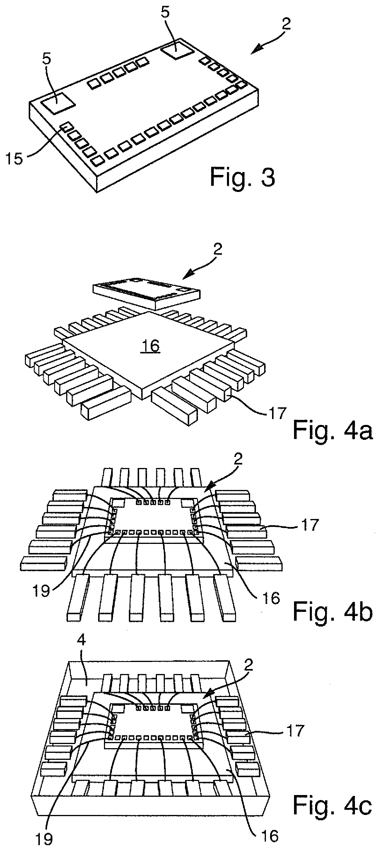
[0022] FIG. 3 a plan view of a semiconductor chip,
[0023] FIG. 4 a) a side view of a semiconductor chip and an exposed pad, b) a side view of a semiconductor chip on an exposed pad, and c) a plan view of a finished semiconductor element,
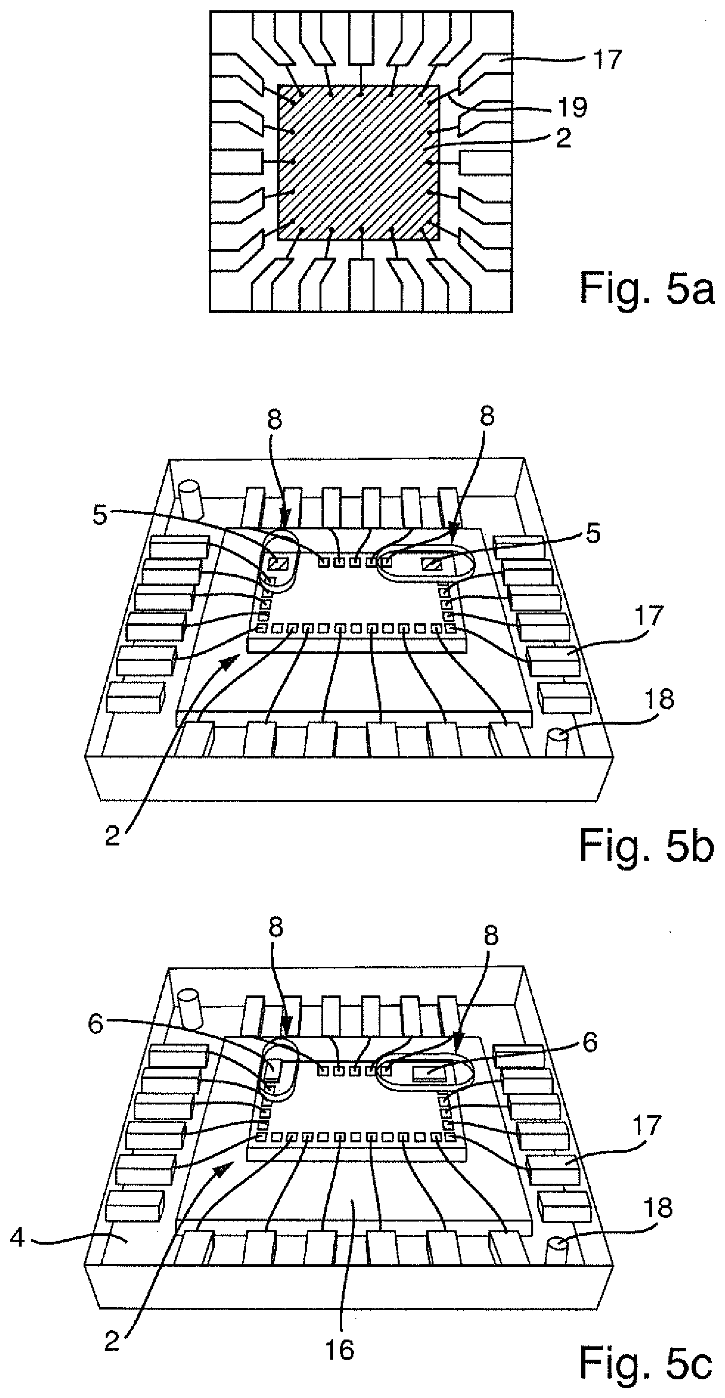
[0024] FIG. 5a) x-ray view of a semiconductor element, b) plan view of a finished semiconductor element with two depressions, and c) plan view of a finished semiconductor element with a first resonator structure in each depression,
[0025] FIG. 6 a side view of a radar based, fill-level sensor with a dielectric lens,
[0026] FIG. 7 a) a side view of a semiconductor element on a printed circuit board and a transition structure, b) a side view of a semiconductor element and transition structure on a printed circuit board, and c) a side view of a transition structure, and
[0027] FIG. 8 a longitudinal section of a radar based, fill-level sensor of FIG. 1 with a dielectric waveguide.
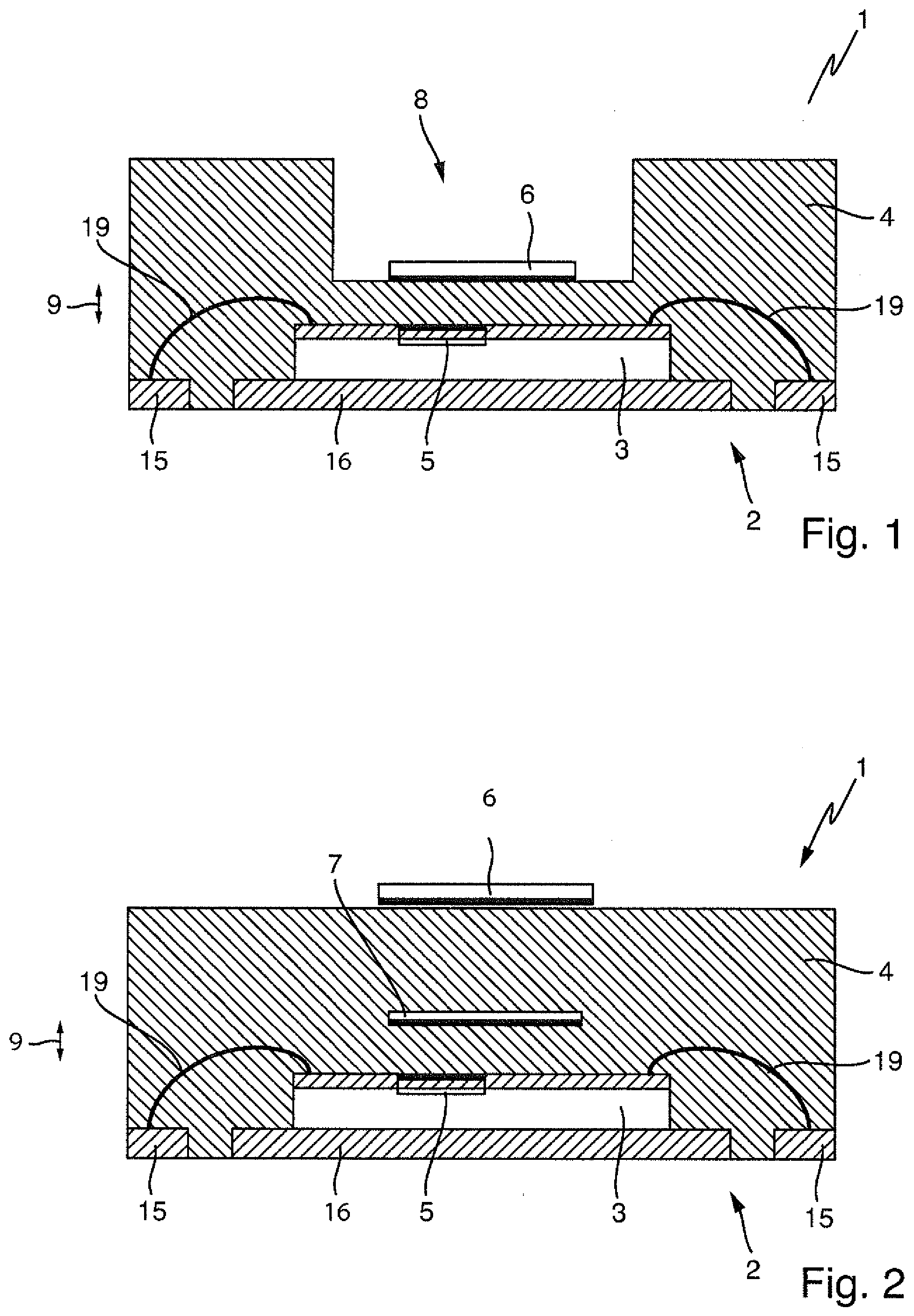
[0028] FIG. 1 shows a cross section of a radar based, fill-level sensor 1 with one semiconductor element 2. The semiconductor element 2 comprises a semiconductor chip 3 and a chip package 4, in which the semiconductor chip 3 is arranged. The semiconductor chip 3 includes a coupling element 5, which serves as signal gate for electromagnetic waves in the millimeter wave region. According to the invention, a first resonator structure 6 is arranged on a surface portion of the chip package 4.
[0029] The chip package 4 includes on the surface portion, on which the first resonator structure 6 is arranged, a depression 8 deepening toward the coupling element 5, so that the separation 9 between the first resonator structure 6 and the coupling element 5 is lessened at the position of the depression 8.
[0030] The coupling element 5 on the semiconductor chip 3 is embodied as a short circuited, very wide, lambda/4 transformer. The radiation into free space occurs via a resonator structure 6, which is embodied as a patch or dielectric resonator structure.
[0031] Furthermore, leads 15 of the chip package 4 are connected by means of bond wires 19 with bond pads of the semiconductor chip 3 for low frequency signals and power supply.
[0032] FIG. 2 shows a cross section of a radar based, fill-level sensor 1 with a semiconductor element 2 comprising first and second resonator structures 6, 7, wherein the second resonator structure 7 is arranged between the coupling element 5 and the first resonator structure 6.
[0033] This is an option supplemental to the embodiment of FIG. 1 and represents a stacked patch arrangement. In such case, before the casting of the chip package 4, a second resonator structure 7 in the form of a small metal substrate platelet was placed over the semiconductor-chip 3. In this way, the process step for producing the depression becomes unnecessary, so that only the first resonator structure 6 still needs to be applied on the package.
[0034] The method of the invention will now be explained in detail based on FIGS. 3-5. By performing the semiconductor processing and sawing the wafer into individual chips, monolithic, integrated semiconductor elements 2 are obtained, on which all circuit parts for producing and processing millimeter wave signals are implemented. The individual semiconductor elements 2 include numerous bond pads 15, via which all analog and digital signals are transmittable at low frequencies.
[0035] Compared to a conventional semiconductor element, the semiconductor element 2 differs only by containing coupler structures in the form of two coupling elements 5 as signal gates at millimeter wave frequencies. The semiconductor element 2 is first installed in a typical chip package, wherein the three steps illustrated in FIGS. 4a-c are performed in the manufacture of the chip packages. In the first step (FIG. 4a), the semiconductor element 2 is adhered to the so-called lead frame, which is composed of the exposed-pad 16 and the leads 17. In the second step (FIG. 4b), the connecting of the bond pads 15 with the leads 17 occurs by means of bond wires 19. In the third step (FIG. 4c), the contacted arrangement is potted with plastic. In this way, the chip package 4 is formed. All three steps are performed in an array of many chips and only after the casting or potting are the chips separated into individual units by sawing or stamping. The steps of the package procedure described to this point correspond to the known state of the art for manufacture of chip packages.
[0036] The steps of the invention are shown in FIGS. 5a-c. In the first step, an x-ray image of the chip package is taken in such a manner that from the x-ray image (FIG. 5a) the exact position of the semiconductor element 2 on the exposed pad 16 and relative to its edges can be ascertained. With the positional data and the known chip layout, then in the second step depressions 8 in the potting material over all coupling elements 5 are produced by means of a material removing method, such as, for example, milling or laser beam machining. Additionally, assembly aids or locators, such as e.g. bores 18, can be formed in the cast material of the package with defined separation from the coupling elements 5. In the depressions 8, finally, in the third step, first resonator structures 6 are introduced, which represent the integrated antennas. In the simplest case, such resonator structures are embodied as resonators in the form of a rectangular metal platelet, whose one edge length corresponds to a half wavelength (resonance length) of the electromagnetic waves in the millimeter wave region. There also exist, however, dielectric resonators, such as, for example, quartz glass, ceramic, plastic or structured substrate platelets, which can be applied. Besides the introduction of prefabricated resonators into the depressions 8, also the deposition of resonator structures by means of 2D/3D printing or MID provide other options.
[0037] The provided depressions 8 have in the method the following central functions:
[0038] a. Producing a defined distance between the first resonator structure 6 and an associated coupling element 5 and therewith the correction of possible thickness fluctuations in the potting material.
[0039] b. Mechanical orientation and securement of the resonator structures.
[0040] c. High electrical coupling between the coupling elements 5 and the associated resonator structures 6 by thinning the layer of potting material, whose thickness in the region of the coupling elements 5 can be less than the loop heights of the bond wires 19.
[0041] By the procedure of the invention using the dimensional relationships ascertained from an x-ray image, the horizontal tolerances of the position of the first resonator structures 6 to the coupling elements 5 can be individually minimized. In case the vertical position tolerances, in spite of the small thickness tolerances of the lead frame and the adhesive layer for the semiconductor mounting are still too large, they can likewise be individually compensated based on a second, vertical, x-ray image.
[0042] The electrical checking of the semiconductor element 2 manufactured according to the method of the invention can be performed with a self-test integrated in the semiconductor chip 3. In such case, a power measurement detects whether the radiation at the first resonator structure 6 on the semiconductor chip 3 is properly functioning or that a malfunction is present at the first resonator structure 6.
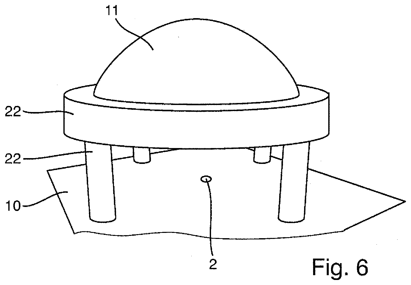
[0043] FIG. 6 shows a semiconductor element 2 arranged on a printed circuit board 10, wherein a dielectric lens 11 is secured on the printed circuit board 10 in such a way that the semiconductor element 2 lies in the focal point of the lens 11. This is an example of an embodiment, in principle, of an application of the semiconductor element 2 with an integrated antenna for sending radiation to the dielectric lens 11, in which case the broad radiation of the integrated antenna is focussed to a highly concentrated beam. The semiconductor element 2 is mounted together with additional electronic assemblies on the printed circuit board 10, wherein its position is so selected that it lies in the focus of the dielectric lens 11, which is connected securely with the printed circuit board 10 by means of a securement arrangement 22. Securement arrangement 22 can also be a housing, in which the printed circuit board 10 is installed.
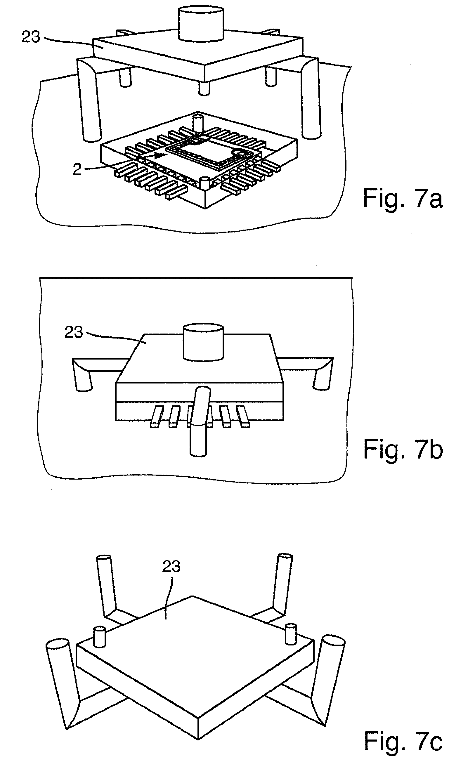
[0044] FIGS. 7a-c show a semiconductor element 2 arranged on a printed circuit board 10, wherein the printed circuit board 10 has a hollow conductor 12 for transferring the electromagnetic waves produced by the semiconductor element 2. Instead of free radiation, the semiconductor element 2 is applied for radiation in-coupling into a hollow conductor 12 with round or rectangular cross section. Necessary for this are specially formed resonators and a transition structure 23 applied supplementally on the package.
[0045] For better evaluation of an x-ray image of the packaged semiconductor element, special marker structures in the vicinity of the coupling elements can be installed in the chip layout, marker structures which because of metal density or pattern show up with especially high contrast in an x-ray image.
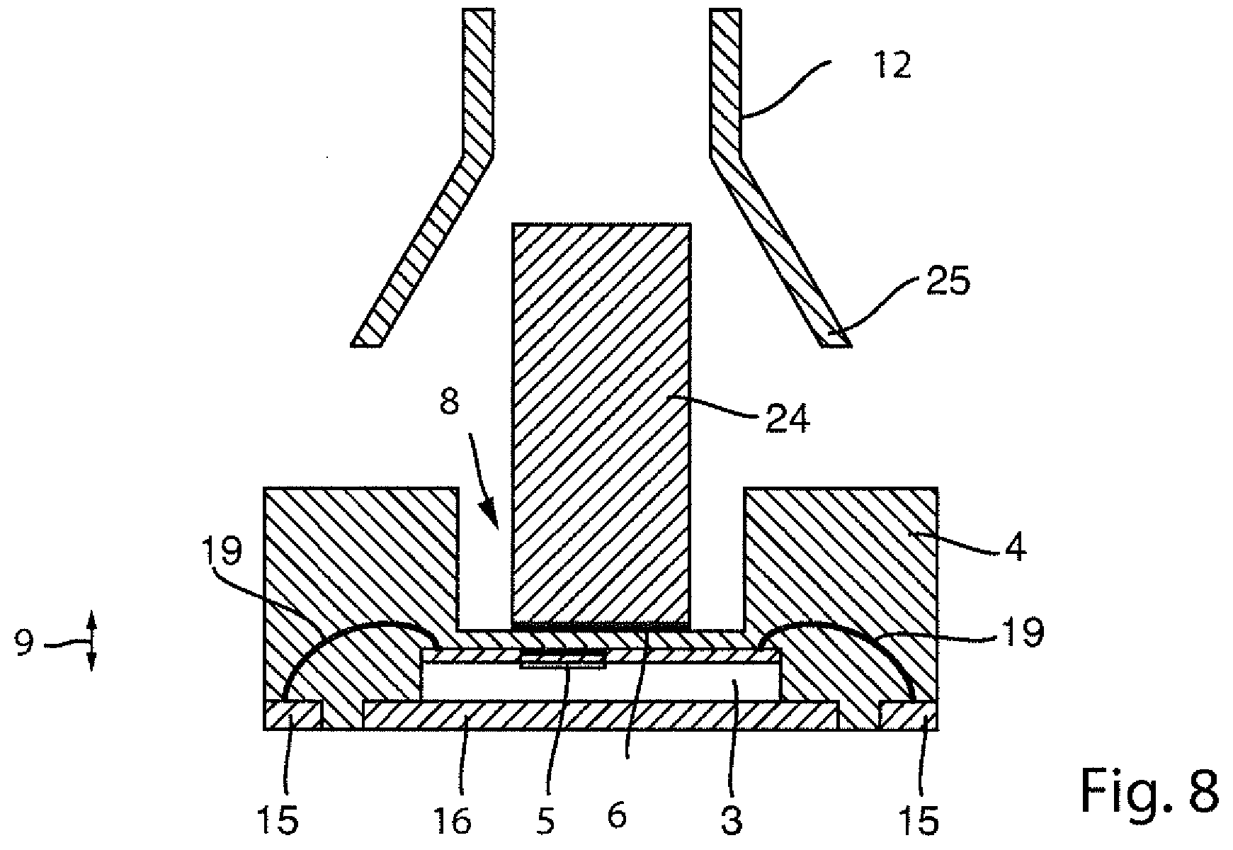
[0046] FIG. 8 shows a longitudinal section of a radar based, fill-level sensor of FIG. 1 with a dielectric waveguide 24 in the depression 8. The dielectric waveguide 24 leads electromagnetic waves, which are out-coupled from the coupling element 5, to the hollow conductor 12 (see FIG. 7a-7c), and electromagnetic waves, which are transmitted from the hollow conductor 12, to the coupling element 5.
[0047] The hollow conductor 12 has a terminal structure 25, which enables a low loss transition via the dielectric waveguide 24 into the hollow conductor 12. The waveguide 24 provides supplementally a galvanic isolation between the radar front end and a metal antenna structure, a feature which in the case of radar device process measurements technology is frequently specified for reasons of Ex protection.
List of Reference Characters
[0048] 1 fill-level sensor
[0049] 2 semiconductor element
[0050] 3 semiconductor chip
[0051] 4 chip package
[0052] 5 coupling element
[0053] 6 first resonator structure
[0054] 7 second resonator structure
[0055] 8 depression
[0056] 9 separation between the first and second resonator structures
[0057] 10 printed circuit board
[0058] 11 lens
[0059] 12 hollow conductor
[0060] 15 lead
[0061] 16 exposed pad
[0062] 18 bore
[0063] 19 bond wire
[0064] 22 securement arrangement
[0065] 23 transition structure
[0066] 24 dielectric waveguide
[0067] 25 terminal structure
* * * * *
D00000
D00001
D00002
D00003
D00004
D00005
D00006
XML
uspto.report is an independent third-party trademark research tool that is not affiliated, endorsed, or sponsored by the United States Patent and Trademark Office (USPTO) or any other governmental organization. The information provided by uspto.report is based on publicly available data at the time of writing and is intended for informational purposes only.
While we strive to provide accurate and up-to-date information, we do not guarantee the accuracy, completeness, reliability, or suitability of the information displayed on this site. The use of this site is at your own risk. Any reliance you place on such information is therefore strictly at your own risk.
All official trademark data, including owner information, should be verified by visiting the official USPTO website at www.uspto.gov. This site is not intended to replace professional legal advice and should not be used as a substitute for consulting with a legal professional who is knowledgeable about trademark law.