Sensor Device
Franke; Jorg
U.S. patent application number 16/750748 was filed with the patent office on 2020-07-30 for sensor device. The applicant listed for this patent is TDK - Micronas GmbH. Invention is credited to Jorg Franke.
| Application Number | 20200241083 16/750748 |
| Document ID | 20200241083 / US20200241083 |
| Family ID | 1000004682804 |
| Filed Date | 2020-07-30 |
| Patent Application | download [pdf] |


| United States Patent Application | 20200241083 |
| Kind Code | A1 |
| Franke; Jorg | July 30, 2020 |
Sensor Device
Abstract
A sensor device (10) is described. The sensor device (10) comprises a laterally arranged double coil (20) with a first coil (30a) and a second coil (30b), wherein first windings (40a) of the first coil (30a) and second windings (40b) of the second coil (40b) are arranged in a spiral shape. The first windings (40a) from a first center point (50a) lead to a common region (60) and the second windings (40b) from a second center point (50b) lead to the common region (60) as well. At least one magnetic field sensor (70, 72a, 72b) is disposed on the laterally arranged double coil (20).
| Inventors: | Franke; Jorg; (Freiburg, DE) | ||||||||||
| Applicant: |
|
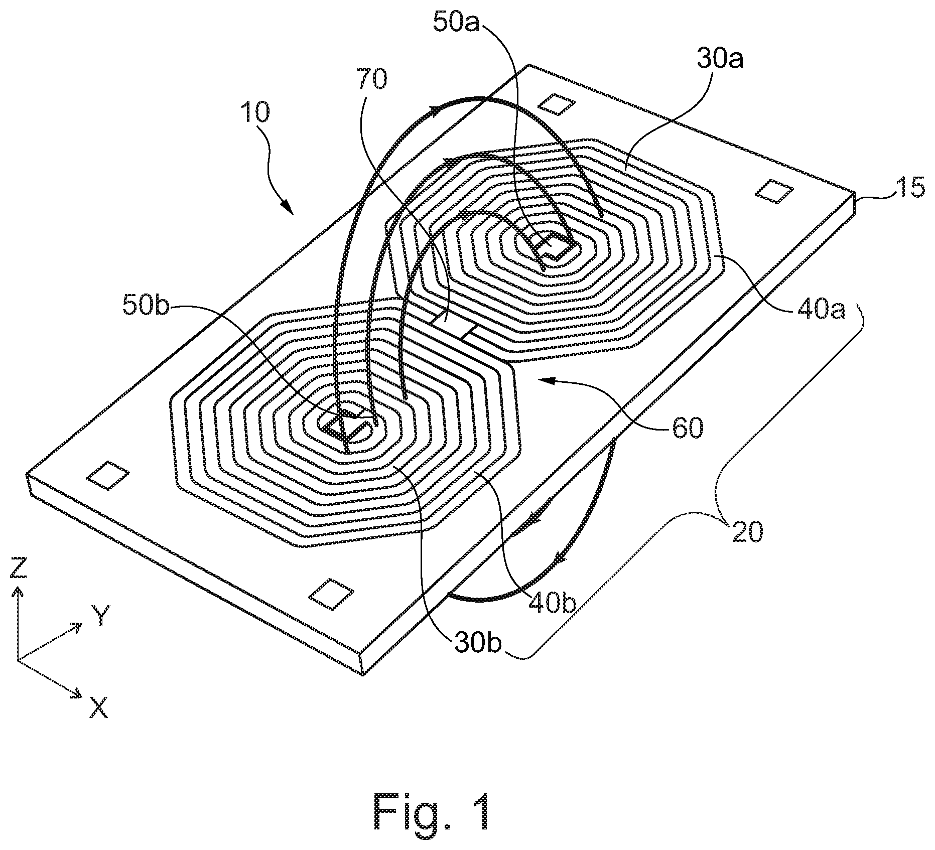
||||||||||
|---|---|---|---|---|---|---|---|---|---|---|---|
| Family ID: | 1000004682804 | ||||||||||
| Appl. No.: | 16/750748 | ||||||||||
| Filed: | January 23, 2020 |
| Current U.S. Class: | 1/1 |
| Current CPC Class: | G01R 33/0094 20130101; G01D 5/145 20130101; H01F 5/04 20130101; G01R 33/0005 20130101; G01R 33/0035 20130101 |
| International Class: | G01R 33/00 20060101 G01R033/00; G01D 5/14 20060101 G01D005/14; H01F 5/04 20060101 H01F005/04 |
Foreign Application Data
| Date | Code | Application Number |
|---|---|---|
| Jan 25, 2019 | DE | 10 2019 101 931.1 |
Claims
1. A sensor device comprising: a laterally arranged double coil with a first coil and a second coil, wherein first windings of the first coil and second windings of the second coil are arranged in a spiral shape and wherein the first windings lead from a first center point to a common region and the second windings lead from a second center point to the common region; and at least one magnetic field sensor disposed on the laterally arranged double coil.
2. The sensor device according to claim 1, wherein the magnetic field sensor is applied to a chip.
3. The sensor device according to claim 1, wherein the magnetic-field sensor is disposed on the double coil.
4. The sensor device according to claim 1, wherein the first windings of the first coil are executed in a same winding direction as the second windings of the second coil.
5. The sensor device according to claim 1, wherein the magnetic field sensor is located in the common region.
6. The sensor device according to claim 1, wherein the magnetic field sensor is at least one of a Hall sensor, a flux gate or an MR sensor.
7. The sensor device according to claim 1, wherein the first center point and the second center point are electrically connected to connectors via bond wires.
8. The sensor device according to claim 1, wherein the first windings of the first coil are executed in the direction contrary to the second windings of the second coil.
Description
CROSS-REFERENCE TO RELATED APPLICATIONS
[0001] This application claims priority to and benefit of German Patent Application No. DE 10 2019 101 931.1 filed on Jan. 29, 2019, the contents of which are incorporated herein by reference in their entirety.
BACKGROUND OF THE INVENTION
Field of the Invention
[0002] The invention relates to a sensor device with a coil.
Brief Description of the Related Art
[0003] Sensor devices of the type mentioned above are known, for example, from the German patent no. DE 11 2010 000 848 B4 (Allegro). In this patent document, a double coil is disclosed, however which has only one winding in each case as a self-text conductor, and wherein each coil of the double coil is located above a z-axis magnetic-field sensor element.
[0004] From the German patent no. DE 10 2011 016 159 B3 the integration of a vertical coil (i.e. repetition of the windings in the z-direction and not in the x- or y-directions) with several windings above a z-axis magnetic field sensor is known. The patent document also discloses the integration of two vertical coils with several windings above a z-axis magnetic-field sensor in each case.
[0005] A different device is also known from the U.S. Pat. No. 7,345,470, which shows a plurality of non-integrated coils for sample testing.
[0006] The state of the art shows solutions for sensor devices with coils with single windings, which limit the possible coil factor and thus also the obtainable magnetic field in relation to the current fed to the coils.
[0007] Moreover, the integration costs for the sensor devices with vertically arranged windings are increased due to the necessary several metal plies or separate coil carriers.
SUMMARY OF THE INVENTION
[0008] The present is a sensor device comprising a laterally arranged double coil with a first coil and a second coil. First windings of the first coil and second windings of the second coils are arranged in a spiral shape on a substrate, and both the first windings and the second windings extend in each case from a first or second center point of the corresponding spiral to a common region. At least one magnetic field sensor is located in a mounted state on the laterally arranged double coil.
[0009] Using this device, the magnetic field sensor can be calibrated well also in the presence of superimposed fields. The arrangement permits a diagnosis in the event of a disturbance of the magnetic field sensors also in an environment with, for example, stray fields.
[0010] The magnetic field sensor is, for example, a Hall sensor, an AMR sensor, a GMR sensor, a flux-gate sensor or a TMR sensor, with the type of magnetic field sensor not being limiting for the invention, however.
DESCRIPTION OF THE DRAWINGS
[0011] For a more complete understanding of the present invention and the advantages thereof, reference is now made to the following description and the accompanying drawings, in which:
[0012] FIG. 1 shows a double coil with a magnetic field sensor and exemplary field lines.
[0013] FIG. 2 shows a double coil with a magnetic field sensor on a die.
[0014] FIG. 3 shows a double coil with two magnetic field sensors and exemplary field lines.
[0015] FIG. 4 shows a sensor arrangement in a conductor carrier (lead frame).
DETAILED DESCRIPTION OF THE INVENTION
[0016] The invention will now be described on the basis of the drawings. It will be understood that the embodiments and aspects of the invention described herein are only examples and do not limit the protective scope of the claims in any way. The invention is defined by the claims and their equivalents. It will be understood that features of one aspect or embodiment of the invention can be combined with a feature of a different aspect or aspects and/or embodiments of the invention.
[0017] FIG. 1 shows a sensor arrangement 10 with a laterally arranged double coil 20 formed of a first coil 30a and a second coil 30b on a substrate 15. The first coil 30a has windings 40a formed in a spiral shape from a first center point 50a of the first coil 30a to a common region 60. The common region 60 is located between the first coil 30a and the second coil 30b and is arranged at the center of the double coil 20. The second coil 30b has second windings 40b formed in a spiral shape from a second center point 50b of the second coil 30b to the common region 60. The first windings 40a and the second windings 40b are shown in FIG. 1 as a clockwise Archimedes spiral, but both could be counterclockwise as well. It is apparent that the second coil 30b is formed from a mirror image of the first coil 30a on the x and y axes.
[0018] The first windings 40a of the first coil 30a and the second windings 40 of the second coil 30b are electrically interconnected at the common region 60. Due to the arrangement of the first windings 40a and of the second windings 40b, the current direction in the first coil 30a and the second coil 30b is in opposite directions. The winding spacings in the first coil 30a and in the second coil 30b are kept as small as possible in order for a current density to be attainable that is as high as possible. Exemplary parameters are 40 .mu.m for the conductor path width of the coils and 2 .mu.m for the spacing of the conductor paths. However, these parameters are not limiting for the invention. Depending on the thicknesses of the metal layer used, the spacings can also be substantially different, however.
[0019] In one aspect of the invention, a magnetic field sensor 70 is located on the upper side of the double coil 20 at the common region 60, i.e. is disposed between the first coil 30a and the second coil 30b. The magnetic field sensor 70 can also be disposed below the double coil 20. The magnetic field sensor 70 is a TMR sensor or a Hall sensor, whereby the choice is not limiting of the invention.
[0020] When current is applied to the double coil 20, one of the first coil 30 or the second coil 30b generates a magnetic field in the z-direction (i.e. perpendicularly to the x-y-plane), and the other one of the first coil 30 or the second coil 30b generates a magnetic field opposite to the z-direction. This results in the current density through the two coils 30a and 30b being amplified at the common region at the magnetic field sensor 70. The generated magnetic field is shown in FIG. 1 as field lines.
[0021] The first center point 50a of the first coil 30a is electrically connected via a first bond wire 90a to a first connector 80a on a lead frame (connection frame/conductor carrier) of a housing 100. The second center point 50b of the second coil 30b is electrically connected via a second bond wire 80b to a second connector 80b of the lead frame of the housing 100. This connection can also be established via conductor paths in a further metal ply. These connections are shown in FIG. 4.
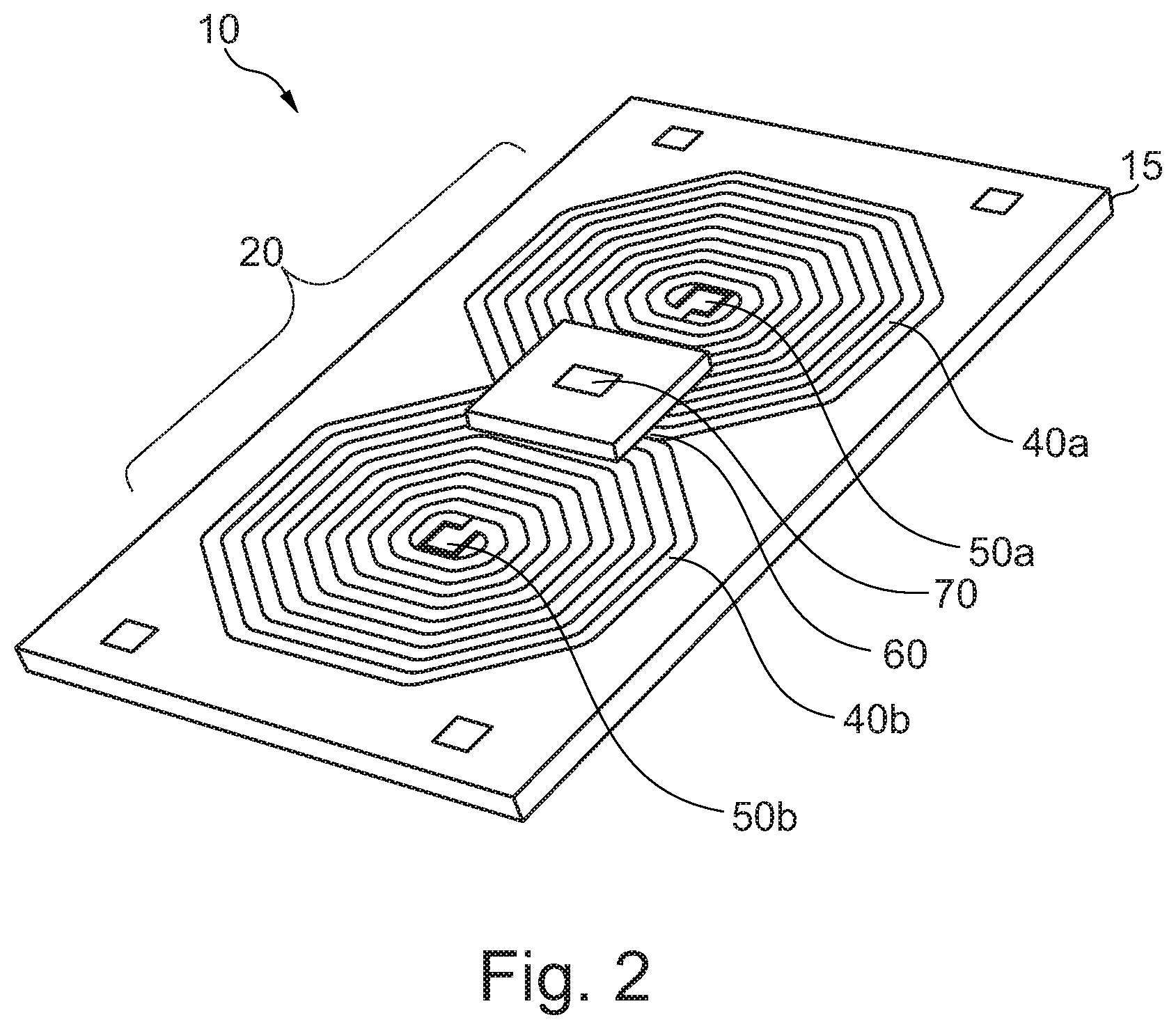
[0022] FIG. 2 shows a further aspect of the invention, in which the magnetic field sensor 70 is applied to a chip 75 (a so-called "die"). In other words, the z-direction is offset from the plane of the double coil.
[0023] FIG. 3 shows a further aspect of the invention, in which two magnetic field sensors 72a and 72b are disposed in each case in the center points 50a and 50b of the corresponding coil 30a and 30b. The two magnetic field sensors 72a and 72b are either located below a bond pad or the two magnetic field sensors 72a and 72b are each an interconnection of several individual sensors of which the common effective point is located below the bond pad. 4 TMR elements in a Wheatstone bridge or 4 magnetic field sensors 72a and 72b connected in parallel for improving the signal-noise ratio could be used, for example.
[0024] In this aspect of the invention, the first coil 30a and the second coil 30b can be configured such that the magnetic field sensors 72a and 72b measure the same field component. In this case, the first coil 30a and the second coil 30b are configured in opposite winding directions, i.e. a clockwise spiral (first windings 40a) and a counterclockwise spiral (second windings 40b). Differently to FIG. 1, the windings are therefore mirrored only on the x-axis. The current direction is consequently in the same direction in the first coil 30a and the second coil 30b and is shown in FIG. 3 by the cross and point symbol.
[0025] In a different aspect of the sensor arrangement shown in FIG. 3, the magnetic-field sensors 72a and 72b are operated differentially and the coils 30a and 30b are configured with windings 40a and 40b with the same winding direction as in FIG. 1, wherein the current direction in the corresponding coils 30a and 30b is contrary.
[0026] FIG. 4 shows the sensor device in a lead frame (connection frame) 100. The first center point 50a and the second center point 50b are electrically connected in each case to connectors 80a, 80b via bond wires 90a, 90b.
[0027] The foregoing description of the preferred embodiment of the invention has been presented for purposes of illustration and description. It is not intended to be exhaustive or to limit the invention to the precise form disclosed, and modifications and variations are possible in light of the above teachings or may be acquired from practice of the invention. The embodiment was chosen and described in order to explain the principles of the invention and its practical application to enable one skilled in the art to utilize the invention in various embodiments as are suited to the particular use contemplated. It is intended that the scope of the invention be defined by the claims appended hereto, and their equivalents. The entirety of each of the aforementioned documents is incorporated by reference herein.
REFERENCE NUMERALS
[0028] 10 sensor device [0029] 15 substrate [0030] 20 double coil [0031] 30a first coil [0032] 30b second coil [0033] 40a first windings [0034] 40b second windings [0035] 50a first center point [0036] 50b second center point [0037] 60 common region [0038] 70 magnetic field sensor [0039] 72a magnetic field sensor [0040] 72b magnetic field sensor [0041] 75 chip [0042] 80a first connector [0043] 80b second connector [0044] 90a first bond wire [0045] 90b second bond wire [0046] 100 housing
* * * * *
D00000
D00001
D00002
D00003
D00004
XML
uspto.report is an independent third-party trademark research tool that is not affiliated, endorsed, or sponsored by the United States Patent and Trademark Office (USPTO) or any other governmental organization. The information provided by uspto.report is based on publicly available data at the time of writing and is intended for informational purposes only.
While we strive to provide accurate and up-to-date information, we do not guarantee the accuracy, completeness, reliability, or suitability of the information displayed on this site. The use of this site is at your own risk. Any reliance you place on such information is therefore strictly at your own risk.
All official trademark data, including owner information, should be verified by visiting the official USPTO website at www.uspto.gov. This site is not intended to replace professional legal advice and should not be used as a substitute for consulting with a legal professional who is knowledgeable about trademark law.