Current Measuring Apparatus
KIKUCHI; Takanori ; et al.
U.S. patent application number 16/635256 was filed with the patent office on 2020-07-23 for current measuring apparatus. The applicant listed for this patent is KOA CORPORATION. Invention is credited to Takanori KIKUCHI, Keishi NAKAMURA, Susumu TOYODA.
| Application Number | 20200233015 16/635256 |
| Document ID | / |
| Family ID | 65272418 |
| Filed Date | 2020-07-23 |


| United States Patent Application | 20200233015 |
| Kind Code | A1 |
| KIKUCHI; Takanori ; et al. | July 23, 2020 |
CURRENT MEASURING APPARATUS
Abstract
Provided is a current measuring apparatus including a current measuring resistor that includes a resistive element and first and second electrodes fixed to the resistive element, the current measuring resistor being adapted to measure a current, and an electronic circuit component including a plurality of terminals. One of the first electrode or the second electrode is used to short at least two of the terminals of the electronic circuit component.
| Inventors: | KIKUCHI; Takanori; (Nagano, JP) ; NAKAMURA; Keishi; (Nagano, JP) ; TOYODA; Susumu; (Nagano, JP) | ||||||||||
| Applicant: |
|
||||||||||
|---|---|---|---|---|---|---|---|---|---|---|---|
| Family ID: | 65272418 | ||||||||||
| Appl. No.: | 16/635256 | ||||||||||
| Filed: | July 10, 2018 | ||||||||||
| PCT Filed: | July 10, 2018 | ||||||||||
| PCT NO: | PCT/JP2018/026019 | ||||||||||
| 371 Date: | January 30, 2020 |
| Current U.S. Class: | 1/1 |
| Current CPC Class: | G01R 1/203 20130101; G01R 19/0092 20130101; G01R 15/00 20130101; G01R 19/0023 20130101 |
| International Class: | G01R 1/20 20060101 G01R001/20; G01R 19/00 20060101 G01R019/00 |
Foreign Application Data
| Date | Code | Application Number |
|---|---|---|
| Aug 10, 2017 | JP | 2017-155656 |
Claims
1. A current measuring apparatus comprising: a current measuring resistor including a resistive element and first and second electrodes fixed to the resistive element, the current measuring resistor being adapted to measure a current; and an electronic circuit component including a plurality of terminals, wherein: one of the first electrode or the second electrode is used to short at least two of the terminals of the electronic circuit component.
2. The current measuring apparatus according to claim 1, wherein the electronic circuit component is packaged.
3. The current measuring apparatus according to claim 1, wherein the plurality of terminals includes a terminal coupled to a semiconductor device packaged in the electronic circuit component.
4. The current measuring apparatus according to claim 1, wherein at least one of the first electrode or the second electrode of the current measuring resistor includes two or more through-holes.
5. The current measuring apparatus according to claim 1, wherein at least one of the first electrode or the second electrode of the current measuring resistor includes an elongated through-hole.
6. The current measuring apparatus according to claim 1, wherein a plurality of electronic components is disposed, and at least one of the first electrode or the second electrode is used to short the two terminals, thereby forming a parallel circuit or a series circuit of the electronic components.
Description
TECHNICAL FIELD
[0001] The present invention relates to current measuring apparatuses.
BACKGROUND ART
[0002] Using high-speed diodes with high performance is necessary to save energy and resources in and increase the reliability of an inverter power supply apparatus. For example, there is known a packaged product including two diodes as an SOT-227 package. Such a product is provided with four terminals.
[0003] Conventionally, such a packaged component is sometimes used with two of its four terminals intentionally shorted depending on its use. To that end, a shorting bar for shorting the two terminals is used. Further, a shunt resistor for sensing a current flow through such a packaged component is sometimes coupled thereto.
[0004] Patent Literature 1 discloses a technique of forming one of terminals of a shunt resistor longer than the other, thereby reducing contact resistance and the like as compared to when a plurality of bus bars is used.
CITATION LIST
Patent Literature
[0005] Patent Literature 1: JP 2016-206138 A
SUMMARY OF INVENTION
Technical Problem
[0006] The shunt resistor disclosed in Patent Literature 1 has a structure in which one of its terminals is longer than the other, and the longer terminal is fixed to a fixation portion of a package (i.e., housing) or the like via a single fixation hole.
[0007] However, Patent Literature 1 fails to disclose how to fix terminals to the housing when two terminals are located on the side of the package.
[0008] It is an object of the present invention to provide a current sensing resistor that is suited to short two terminals of a predetermined electronic circuit component having a plurality of terminals and sense a current flow therethrough, and a current measuring apparatus including such a current sensing resistor.
[0009] According to an aspect of the present invention, a current measuring apparatus is provided that includes a current measuring resistor including a resistive element and first and second electrodes fixed to the resistive element, the current measuring resistor being adapted to measure a current, and an electronic circuit component including a plurality of terminals, in which one of the first electrode or the second electrode is used to short at least two of the terminals of the electronic circuit component.
[0010] The electronic circuit component is preferably packaged. The package is an SOT 227 package, for example.
[0011] The plurality of terminals preferably includes a terminal coupled to a semiconductor device packaged in the electronic circuit component.
[0012] At least one of the first electrode or the second electrode of the current measuring resistor includes two or more through-holes.
[0013] At least one of the first electrode or the second electrode of the current measuring resistor includes an elongated through-hole.
[0014] A plurality of electronic components is disposed in the package, and at least one of the first electrode or the second electrode is used to short the two terminals, thereby forming a parallel circuit or a series circuit of the electronic components.
[0015] In addition, the present invention provides a current measuring resistor including a resistive element and first and second electrodes fixed to the resistive element, the current measuring resistor being adapted to measure a current, in which at least one of the first electrode or the second electrode includes two or more through-holes.
[0016] In addition, the present invention provides a current measuring resistor including a resistive element and first and second electrodes fixed to the resistive element, the current measuring resistor being adapted to measure a current, in which at least one of the first electrode or the second electrode includes an elongated through-hole.
[0017] The present specification incorporates the disclosure of JP Patent Application No. 2017-155656 that forms the basis of the priority claim of the present application.
Advantageous Effects of Invention
[0018] The present invention can provide a current sensing resistor that is suited to short two terminals of a package and sense a current flow therethrough, and a current measuring apparatus including the same.
BRIEF DESCRIPTION OF DRAWINGS
[0019] FIG. 1 are a plan view of an exemplary configuration of a current measuring resistor and a current measuring apparatus including the same according to a first embodiment of the present invention, and a cross-sectional view of the shunt resistor.
[0020] FIG. 2 is an equivalent circuit diagram of an SOT 227 package.
[0021] FIG. 3 is an equivalent circuit diagram of FIG. 1.
[0022] FIG. 4 is a circuit diagram of the modified example of FIG. 3.
[0023] FIGS. 5(a) and 5(b) are plan views of the modified examples of FIG. 1.
[0024] FIGS. 6A(a) and 6A(b) are plan views of the modified examples of FIG. 5, and a cross-sectional view of the shunt resistor.
[0025] FIG. 6B(c) is a plan view of the modified example of FIG. 6A(a), FIG. 6B(d) is a plan view and a cross-sectional view of another example of the shunt resistor, and FIG. 6B(e) is a plan view of an implementation of the shunt resistor in FIG. 6B(d).
[0026] FIG. 7 is a cross-sectional view of an exemplary configuration of a lead frame-integrated shunt resistor of the present embodiment according to a second embodiment of the present invention.
[0027] FIG. 8 is a plan view of FIG. 7.
DESCRIPTION OF EMBODIMENTS
[0028] Hereinafter, a current measuring resistor (i.e., shunt resistor) and a current measuring apparatus including the same according to an embodiment of the present invention will be described in detail with reference to the drawings.
[0029] In this specification, a direction in which electrodes are arranged at opposite ends of a resistive element shall be referred to as a "length direction" and a direction intersecting the length direction shall be referred to as a "width direction."
First Embodiment
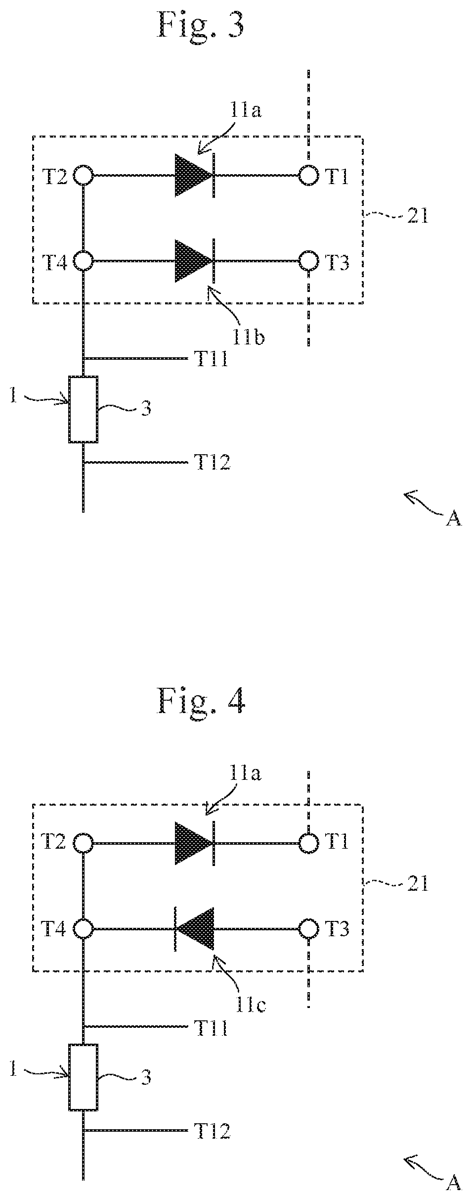
[0030] First, a first embodiment of the present invention will be described. FIG. 1 are a plan view of an exemplary configuration of a current measuring resistor and a current measuring apparatus including the same according to the present embodiment, and a cross-sectional view of the shunt resistor. A current measuring apparatus A illustrated in FIG. 1 includes a shunt resistor 1 and an SOT 227 package 21 as an exemplary electronic circuit component, for example. FIG. 2 is an equivalent circuit diagram of the package 21, and FIG. 3 is an equivalent circuit diagram of FIG. 1.
[0031] As illustrated in FIGS. 1 and 2, the package 21 has four terminals including a terminal T1 to a terminal T4. A diode device 11a is arranged between the terminal T1 and the terminal T2. Also, a diode device 11b is arranged between the terminal T3 and the terminal T4 in the forward direction like the diode device 11a. The two diode devices may also be arranged in opposite directions. That is, the two diode devices may be arranged in parallel in the forward direction and the reverse direction, respectively. Although this example describes the SOT 227 package including packaged diode devices, the configuration of the package and the elements incorporated therein are not limited thereto, and a variety of examples, such as switching elements, are considered.
[0032] The shunt resistor 1 illustrated in FIG. 1 includes a resistive element 3 and a first electrode 5a and a second electrode 5b on opposite sides thereof. Terminals T11 and T12 for sensing a voltage are arranged around portions where the electrodes 5a and 5b are coupled to the resistive element 3, respectively. The terminals T11 and T12 are omitted in some of the other drawings. The shunt resistor 1 illustrated herein is a resistor with a so-called butt-joint structure that is obtained by butt-joining the resistive element and the electrodes together at end faces of their metal materials, but the structure of the shunt resistor 1 is not limited thereto.
[0033] For the resistive element 3, a metal plate material, such as a Cu--Ni, Cu--Mn, or Ni--Cr-based material, can be used. For the electrodes, a material, such as Cu, can be used.
[0034] In the shunt resistor 1, the length L1 of the first electrode 5a is greater than the length L2 of the second electrode 5b. Each of the first electrode 5a and the second electrode 5b is provided with a fixation hole through which the package 21 and the shunt resistor 1 are adapted to be fixed together. The first electrode 5a is provided with two fixation holes 7x and 7y. The second electrode 5b is provided with one fixation hole 7z.
[0035] As illustrated in FIGS. 1 and 3, in the current measuring apparatus according to the present embodiment, the terminal T2 of the package 21 is fastened to the shunt resistor 1 with a screw via the fixation hole 7x in the first electrode 5a of the shunt resistor 1, for example. In addition, the terminal T4 of the package 21 is fastened to the shunt resistor 1 with a screw via the fixation hole 7y in the first electrode 5a of the shunt resistor 1, for example.
[0036] FIG. 3 illustrates an equivalent circuit diagram of the current measuring apparatus A illustrated in FIG. 1. That is, the terminal T2 and the terminal T4 are shorted.
[0037] A current flow through the package 21 can be measured from a voltage across the terminals T11 and T12 sandwiching the resistive element 3 of the shunt resistor 1.
[0038] It should be noted that a current flow through the package 21 can be similarly measured using a configuration in which the diode device 11a and the diode device 11c are arranged in opposite directions as illustrated in FIG. 4.
[0039] In the configuration illustrated in FIG. 1, in order not to short the terminals of the package 21, the position of the shunt resistor 1 may be inverted from that in FIG. 1 as illustrated in FIG. 5(a) so that the fixation hole 7z is fixed to the terminal T4 (i.e., the shunt resistor located in the lower position), or the position of the shunt resistor 1 may be shifted in the horizontal direction as illustrated in FIG. 5(b) so that the fixation hole 7x is fixed to the terminal T4.
[0040] In addition, as illustrated in FIG. 6A(a), one of the electrodes (5a) of the shunt resistor 1 may have formed therein an elongated hole 7w with an elliptical shape that is long in the length direction so that the two terminals T2 and T4 of the package 21 are fixed through the elongated hole 7w.
[0041] Further, as illustrated in FIGS. 6A(b) and 6B(c), the shunt resistor 1 with the elongated hole illustrated in FIG. 6A(a) may be used while the position of the shunt resistor 1 is inverted so that the elongated hole 7w is disposed on the right side of FIG. 6A(b), or the position of the elongated hole 7w may be shifted in the horizontal direction.
[0042] FIG. 6B(d) is a plan view of another example of the shunt resistor 1. In the example, the elongated hole 7w is formed penetrating through the electrode 5a. A part of the elongated hole 7w has an opening 8 formed at an end of the electrode 5a. The other configurations are similar to those of the other examples.
[0043] FIG. 6B(e) illustrates an implementation of the shunt resistor in FIG. 6B(d). In the present implementation, the terminals T2 and T4 of the package 21 are shorted by the electrode 5a. In addition, the shunt resistor 1 may be slid so as to be coupled to the package 21 as illustrated in FIG. 6B(c). The elongated hole 7w has the opening 8. Therefore, when the shunt resistor or a wire (not illustrated) is fastened to the package 21 using bolts (not illustrated) through the threaded holes 35 of the terminals T2 and T4, the bolts may be temporarily fixed in the threaded holes 35 so that the electrode 5a of the shunt resistor 1 may be slid between the flange heads of the bolts and the terminals T2 and T4 from the lateral side. This allows the shunt resistor to be easily installed.
[0044] As described above, to sense a current using a shunt resistor, it has been necessary to prepare two parts including a shunt resistor to be used for sensing a current, and a shorting bar for shorting two terminals. In contrast, providing two threaded holes or an elongated elliptical hole in an electrode on the side to be coupled to the package can add the function of a shorting bar for shorting two terminals to the shunt resistor for sensing a current. Meanwhile, even when the two terminals need not be shorted, shifting or inverting the shunt resistor allows the shunt resistor to be used as the same shunt resistor.
Second Embodiment
[0045] As the development of power semiconductors, such as SiC and GaN, progresses, a semiconductor chip may sometimes be used with its upper face directly coupled to a copper wire in the shape of a lead frame. Providing such a lead frame with some functions is also useful from the perspective of reducing the size of the apparatus. The present embodiment relates to a structure obtained by applying the present invention to sensing of a current that is controlled with such a power semiconductor.
[0046] FIG. 7 is a cross-sectional view of an exemplary configuration of a power module as an exemplary electronic circuit component including the shunt resistor according to the present embodiment, and FIG. 8 is a plan view thereof. As illustrated in FIGS. 7 and 8, the lead frame-integrated shunt resistor according to the present embodiment includes a shunt portion (i.e., left side in the drawing) and a shorted portion (i.e., right side in the drawing) provided in the package.
[0047] The structure of the power module will be described in more detail. The first wire 53a, the second wire 53b, and the third wire 53c are provided on a ceramic substrate 51. The first wire 53a is provided with a first semiconductor device 61 with a conductive adhesive 55 interposed therebetween. The second wire 53b is provided with a second semiconductor device 63 with a conductive adhesive 57 interposed therebetween. The adhesive is a fixing agent for packaging, and is adapted to fix the semiconductor devices to a circuit pattern. Examples include solder, sintered Cu, and sintered Ag.
[0048] Meanwhile, the lower face of the ceramic substrate 51 has a metal layer 81 formed thereon, and the metal layer 81 is further coupled to a radiator plate 85 via an adhesive 83.
[0049] In addition, a copper wire 31a in the shape of a lead frame is disposed between the first wire 53a and the second wire 53b. The shunt resistor 1 in the shape of a lead frame is also disposed between the first wire 53a and the third wire 53c. The shunt resistor 1 includes a resistive element 3 and electrodes 5a and 5b at opposite ends thereof as in the first embodiment. The wire 31a partially forms the electrode 5a, and a portion where the electrode 5a is coupled to the first wire 53a and the second wire 53b corresponds to the wire 31a. The wire 31a is coupled to the first wire 53a and the second wire 53b via the semiconductor devices 61 and 63, respectively. Each of the semiconductor devices 61 and 63 has a terminal coupled to the first wire 53a or the second wire 53b, and a terminal coupled to the wire 31a. The wire 31a and a wire on the side of the substrate (i.e., a terminal functioning as a portion to be coupled of the wire) may be directly coupled together without the intermediary of any semiconductor device. The wire 31a and the terminal are coupled together using solder, an electrically conducting adhesive, or the like. It should be noted that in the drawing, other electrical elements (i.e., microcomputer), wire patterns, external connection electrodes, an external package, and the like are omitted.
[0050] Further, wires 73 and 75 are coupled to the electrodes 5a and 5b around the resistive element 3, respectively, with bonding wires.
[0051] As described above, when the shunt resistor 1 is subjected to surface treatment and is coupled to the wires 73 and 75 by wire bonding, for example, so as to be able to sense a voltage, it becomes possible to directly send a signal to a portion where a voltage signal is needed. Among the structure of the shunt resistor 1, the electrode 5b as one of the electrodes functions to short the terminals of the chips of the first and second semiconductors 61 and 63. The other electrode 5a is coupled to the third wire 53c forming a current path. The shunt resistor 1 is formed in the shape of a thin plate, and has a plurality of bent portions. This can absorb stress due to thermal shrinkage of the substrate, and thus enables stable electrical connection. The shunt resistor 1 need not have such bent portions depending on the materials of the substrate, use conditions, and the like.
[0052] As described above, according to the present embodiment, a current to be monitored is flowed through the shunt resistor 1 (i.e., a resistor with a low resistance value that is less than or equal to several m.OMEGA.), and a voltage generated across the electrodes 5a and 5b at opposite ends of the shunt resistor 1 is measured. The shunt resistor 1 can be used for a current measuring apparatus that senses a current from a known resistance value, and has the following advantageous effects.
[0053] A substrate specifically designed to radiate heat is used for a module for controlling a large current, which is called an IPM (intelligent power module). A plurality of power semiconductors is mounted on the substrate.
[0054] To couple the power semiconductors to the substrate, radiation of heat should be fully considered. Therefore, wires for current are not provided on the substrate but the upper faces of the chips are directly coupled together with a copper frame in the shape of a lead frame. Thus, using a part of the copper plate in the shape of a lead frame as a shunt resistor can add a current sensing function to the copper wire other than the function of an electric wire and thus can reduce the number of components. A single shunt resistor can be used to electrically couple two terminals of an electronic circuit component that includes at least three terminals, and measure a current flow between terminals other than the two terminals.
[0055] In the aforementioned embodiment, the configurations and the like illustrated in the drawings are not limited thereto and can be changed as appropriate within the range that the advantageous effects of the present invention can be exerted. Besides, the present invention can be implemented with the configurations and the like changed as appropriate without departing from the object of the present invention.
[0056] The constituent elements of the present invention can be freely selected or not selected, and an invention including the selected configurations is included in the present invention.
INDUSTRIAL APPLICABILITY
[0057] The present invention is applicable to current measuring apparatuses used for a variety of electrical apparatuses.
REFERENCE SIGNS LIST
[0058] A Current measuring apparatus [0059] T1 to T4 Terminal [0060] 1 Shunt resistor [0061] 3 Resistive element [0062] 5a First electrode [0063] 5b Second electrode [0064] 7x, 7y, 7z Fixation holes [0065] 11a, 11b Diode device [0066] 21 Package [0067] 51 Ceramic substrate [0068] 53a First wire [0069] 53b Second wire [0070] 53c Third wire [0071] 57 Adhesive [0072] 61 First semiconductor device [0073] 63 Second semiconductor device [0074] 73, 75 Wire [0075] 81 Metal layer [0076] 83 Adhesive [0077] 85 Radiator plate
[0078] All publications, patents, and patent applications cited in this specification are incorporated herein by reference in their entirety.
* * * * *
D00000
D00001
D00002
D00003
D00004
D00005
D00006
XML
uspto.report is an independent third-party trademark research tool that is not affiliated, endorsed, or sponsored by the United States Patent and Trademark Office (USPTO) or any other governmental organization. The information provided by uspto.report is based on publicly available data at the time of writing and is intended for informational purposes only.
While we strive to provide accurate and up-to-date information, we do not guarantee the accuracy, completeness, reliability, or suitability of the information displayed on this site. The use of this site is at your own risk. Any reliance you place on such information is therefore strictly at your own risk.
All official trademark data, including owner information, should be verified by visiting the official USPTO website at www.uspto.gov. This site is not intended to replace professional legal advice and should not be used as a substitute for consulting with a legal professional who is knowledgeable about trademark law.