Multi-radio Access Technology Envelope Tracking Amplifier Apparatus
Khlat; Nadim
U.S. patent application number 16/689236 was filed with the patent office on 2020-07-16 for multi-radio access technology envelope tracking amplifier apparatus. The applicant listed for this patent is Qorvo US, Inc.. Invention is credited to Nadim Khlat.
| Application Number | 20200228063 16/689236 |
| Document ID | 20200228063 / US20200228063 |
| Family ID | 71516880 |
| Filed Date | 2020-07-16 |
| Patent Application | download [pdf] |


| United States Patent Application | 20200228063 |
| Kind Code | A1 |
| Khlat; Nadim | July 16, 2020 |
MULTI-RADIO ACCESS TECHNOLOGY ENVELOPE TRACKING AMPLIFIER APPARATUS
Abstract
A multi-radio access technology (RAT) envelope tracking (ET) amplifier apparatus is provided. The multi-RAT ET amplifier apparatus may be configured to enable concurrent communication of at least two radio frequency (RF) signals associated with at least two different RATs. Specifically, the multi-RAT ET amplifier apparatus includes an ET integrated circuit (IC) (ETIC) and a distributed ETIC (DETIC) configured to generate respective ET voltages for amplifying the two RF signals. In addition, the DETIC can be configured to utilize certain circuit(s) in the ETIC to help reduce a footprint of the DETIC. By amplifying the two different RF signals based on the respective ET voltages and sharing certain circuit(s) between the ETIC and the DETIC, it may be possible to improve overall efficiency and heat dissipation in the multi-RAT ET amplifier apparatus concurrent to reducing the footprint of the DETIC.
| Inventors: | Khlat; Nadim; (Cugnaux, FR) | ||||||||||
| Applicant: |
|
||||||||||
|---|---|---|---|---|---|---|---|---|---|---|---|
| Family ID: | 71516880 | ||||||||||
| Appl. No.: | 16/689236 | ||||||||||
| Filed: | November 20, 2019 |
Related U.S. Patent Documents
| Application Number | Filing Date | Patent Number | ||
|---|---|---|---|---|
| 62792750 | Jan 15, 2019 | |||
| Current U.S. Class: | 1/1 |
| Current CPC Class: | H04B 2001/045 20130101; H03F 2200/451 20130101; H03F 1/02 20130101; H03F 3/19 20130101; H04B 1/04 20130101; H03F 2200/102 20130101 |
| International Class: | H03F 1/02 20060101 H03F001/02; H03F 3/19 20060101 H03F003/19; H04B 1/04 20060101 H04B001/04 |
Claims
1. A multi-radio access technology (multi-RAT) envelope tracking (ET) amplifier apparatus comprising: an ET integrated circuit (IC) (ETIC) comprising: at least two primary ports coupled to at least two amplifier circuits configured to amplify a first radio frequency (RF) signal corresponding to a first radio access technology (RAT) based on at least two ET voltages, respectively; and at least two voltage circuits configured to generate the at least two ET voltages at the at least two primary ports, respectively; and a distributed ETIC (DETIC) coupled to a distributed amplifier circuit configured to amplify a second RF signal corresponding to a second RAT different from the first RAT based on a distributed ET voltage, the DETIC comprising a distributed voltage circuit configured to generate the distributed ET voltage.
2. The multi-RAT ET amplifier apparatus of claim 1 wherein the ETIC and the DETIC are configured to generate the at least two ET voltages and the distributed ET voltage concurrently.
3. The multi-RAT ET amplifier apparatus of claim 2 further comprising the at least two amplifier circuits and the distributed amplifier circuit configured to amplify the first RF signal and the second RF signal concurrently based on the at least two ET voltages and the distributed ET voltage.
4. The multi-RAT ET amplifier apparatus of claim 1 wherein: the first RAT corresponds to a licensed-band RAT selected from the group consisting of: a third-generation (3G) RAT, a fourth-generation (4G) RAT, a fifth-generation (5G) RAT, and a 5G new-radio (5G-NR) RAT; and the second RAT corresponds to an unlicensed-band RAT selected from the group consisting of: Wi-Fi and enhanced licensed assisted access (eLAA).
5. The multi-RAT ET amplifier apparatus of claim 1 wherein the ETIC and the DETIC are provided in different dies.
6. The multi-RAT ET amplifier apparatus of claim 1 wherein each of the at least two voltage circuits and the distributed voltage circuit comprise: a voltage amplifier configured to generate an initial ET voltage based on an ET target voltage and a supply voltage; and an offset capacitor configured to raise the initial ET voltage by an offset voltage to generate a respective ET voltage among the at least two ET voltages and the distributed ET voltage.
7. The multi-RAT ET amplifier apparatus of claim 6 wherein the ETIC further comprises a supply voltage circuit configured to generate the supply voltage at a plurality of supply voltage levels.
8. The multi-RAT ET amplifier apparatus of claim 1 wherein the ETIC further comprises: an auxiliary port coupled to the DETIC; at least two tracker circuits configured to provide at least two low-frequency currents to the at least two primary ports, respectively; and an auxiliary tracker circuit configured to provide a distributed low-frequency current to the auxiliary port.
9. The multi-RAT ET amplifier apparatus of claim 8 wherein the at least two tracker circuits and the auxiliary tracker circuit each comprise: a multi-level charge pump (MCP) configured to generate a low-frequency voltage at a plurality of voltage levels based on a battery voltage; and a power inductor configured to generate a respective low-frequency current among the at least two low-frequency currents and the distributed low-frequency current based on the low-frequency voltage.
10. The multi-RAT ET amplifier apparatus of claim 8 wherein: the distributed amplifier circuit comprises an input stage and an output stage; and the DETIC is further configured to: provide the distributed ET voltage and the distributed low-frequency current to the output stage; and provide a distributed constant voltage to the input stage.
11. The multi-RAT ET amplifier apparatus of claim 10 wherein the DETIC is further configured to receive the distributed constant voltage from the ETIC.
12. The multi-RAT ET amplifier apparatus of claim 10 wherein the DETIC further comprises a distributed low-dropout regulator (DLDO) configured to generate the distributed constant voltage.
13. The multi-RAT ET amplifier apparatus of claim 10 wherein the DETIC is further configured to provide the distributed constant voltage to a secondary distributed amplifier circuit configured to amplify a Wi-Fi 2.4 GHz band RF signal.
14. The multi-RAT ET amplifier apparatus of claim 10 wherein the ETIC further comprises: a secondary port coupled to a secondary amplifier circuit configured to amplify a third RF signal associated with a second-generation (2G) RAT based on a constant voltage; and a low-dropout regulator (LDO) configured to provide the constant voltage to the secondary port.
15. The multi-RAT ET amplifier apparatus of claim 8 further comprising a second DETIC configured to provide a second distributed ET voltage to a second distributed amplifier circuit configured to amplify the second RF signal, wherein the distributed amplifier circuit and the second distributed amplifier circuit are configured to amplify the second RF signal concurrently.
16. The multi-RAT ET amplifier apparatus of claim 15 wherein: the second distributed amplifier circuit comprises a second input stage and a second output stage; and the second DETIC is further configured to: provide the second distributed ET voltage to the second output stage; and provide a second distributed constant voltage to the second input stage.
17. The multi-RAT ET amplifier apparatus of claim 16 wherein the second DETIC is further configured to receive the second distributed constant voltage from the ETIC.
18. The multi-RAT ET amplifier apparatus of claim 16 wherein the second DETIC further comprises a second distributed low-dropout regulator (DLDO) configured to generate the second distributed constant voltage.
19. The multi-RAT ET amplifier apparatus of claim 16 wherein the second DETIC is further configured to: receive the distributed low-frequency current from the auxiliary port; and provide the distributed low-frequency current to the second output stage.
20. The multi-RAT ET amplifier apparatus of claim 16 wherein: the ETIC further comprises: a second auxiliary port coupled to the second DETIC; and a second auxiliary tracker circuit configured to provide a second distributed low-frequency current to the second auxiliary port; and the second DETIC is further configured to provide the second distributed low-frequency current to the second output stage.
Description
RELATED APPLICATIONS
[0001] This application claims the benefit of provisional patent application Ser. No. 62/792,750, filed Jan. 15, 2019, the disclosure of which is hereby incorporated herein by reference in its entirety.
FIELD OF THE DISCLOSURE
[0002] The technology of the disclosure relates generally to an amplifier apparatus configured to amplify a radio frequency (RF) signal(s) corresponding to multiple radio access technologies (RATs).
BACKGROUND
[0003] Mobile communication devices have become increasingly common in current society for providing wireless communication services. The prevalence of these mobile communication devices is driven in part by the many functions that are now enabled on such devices. Increased processing capabilities in such devices means that mobile communication devices have evolved from being pure communication tools into sophisticated mobile multimedia centers that enable enhanced user experiences.
[0004] Fifth-generation (5G) wireless communication technology has been widely regarded as a new generation of radio access technology (RAT) that will go beyond the conventional second-generation (2G), third-generation (3G), and fourth-generation (4G) RATs. The 5G RAT is expected to deliver significantly higher data rates, improved coverage range, enhanced signaling efficiency, and reduced latency compared to the conventional 2G, 3G, and 4G RATs. A 5G-capable mobile communication device is typically a multi-RAT communication device configured to provide continued support to the conventional 4G, 3G, or even 2G RATs for geographic coverage and backward compatibility reasons, in addition to communicating based on the 5G RAT. Furthermore, the 5G-capable mobile communication device also needs to support Wi-Fi technology, as defined by the Institute of Electrical and Electronics Engineers (IEEE) 802.11 Working Group, to help improve indoor coverage and/or to enable such cross-RAT wireless communication standards as the enhanced Licensed Assisted Access (eLAA).
[0005] The 5G-capable mobile communication device is typically required (e.g., by regulatory authority, industrial standard, and/or design specification) to transmit a wireless communication signal(s) in a specific RAT based on a specific power. As such, the 5G-capable mobile communication device typically employs a power amplifier(s) to amplify the wireless communication signal(s) to the specific power prior to transmission. Envelope tracking (ET) is a technology designed to improve operating efficiency of the power amplifier(s) to help reduce power consumption and thermal dissipation in the 5G-capable mobile communication device. In this regard, it may be desirable to configure the power amplifier(s) to consistently improve operating efficiency across different RATs.
SUMMARY
[0006] Embodiments of the disclosure relate to a multi-radio access technology (RAT) envelope tracking (ET) amplifier apparatus. In examples discussed herein, the multi-RAT ET amplifier apparatus can be configured to enable concurrent communication of at least two radio frequency (RF) signals associated with at least two different RATs. Specifically, the multi-RAT ET amplifier apparatus includes an ET integrated circuit (IC) (ETIC) and a distributed ETIC (DETIC). In a non-limiting example, the ETIC is configured to generate at least two ET voltages for amplifying a first RF signal(s) associated with a first RAT, while the DETIC is configured to generate a distributed ET voltage for amplifying a second RF signal(s) associated with a second RAT. The ETIC and the DETIC may be configured to generate the ET voltages and the distributed ET voltage concurrently such that the two RF signals can be amplified and transmitted concurrently. In addition, the DETIC can be configured to utilize certain circuit(s) in the ETIC to help reduce a footprint of the DETIC. By amplifying the two different RF signals based on respective ET voltages and sharing certain circuit(s) between the ETIC and the DETIC, it may be possible to improve overall efficiency and heat dissipation in the multi-RAT ET amplifier apparatus concurrent to reducing the footprint of the DETIC.
[0007] In one aspect, a multi-RAT ET amplifier apparatus is provided. The multi-RAT ET amplifier apparatus includes and ETIC. The ETIC includes at least two primary ports coupled to at least two amplifier circuits configured to amplify a first RF signal corresponding to a first RAT based on at least two ET voltages, respectively. The ETIC also includes at least two voltage circuits configured to generate the ET voltages at the primary ports, respectively. The multi-RAT ET amplifier apparatus also includes a DETIC coupled to a distributed amplifier circuit configured to amplify a second RF signal corresponding to a second RAT different from the first RAT based on a distributed ET voltage. The DETIC includes a distributed voltage circuit configured to generate the distributed ET voltage.
[0008] Those skilled in the art will appreciate the scope of the present disclosure and realize additional aspects thereof after reading the following detailed description of the preferred embodiments in association with the accompanying drawing figures.
BRIEF DESCRIPTION OF THE DRAWING FIGURES
[0009] The accompanying drawing figures incorporated in and forming a part of this specification illustrate several aspects of the disclosure, and together with the description serve to explain the principles of the disclosure.
[0010] FIG. 1 is a schematic diagram of an exemplary multi-RAT ET amplifier apparatus configured according to an embodiment of the present disclosure;
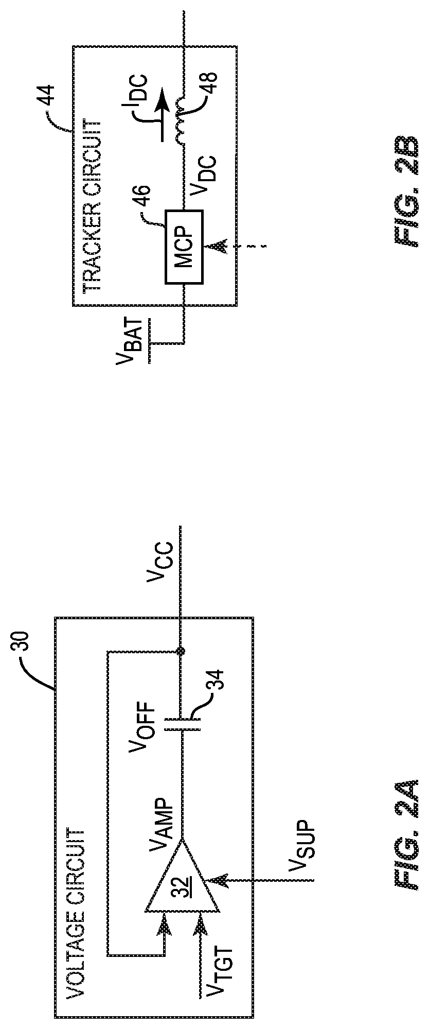
[0011] FIG. 2A is a schematic diagram of an exemplary voltage circuit that can be provided in the multi-RAT ET amplifier apparatus of FIG. 1;
[0012] FIG. 2B is a schematic diagram of an exemplary tracker circuit that can be provided in the multi-RAT ET amplifier apparatus of FIG. 1;
[0013] FIG. 3 is a schematic diagram of an exemplary multi-RAT ET amplifier apparatus configured according to another embodiment of the present disclosure; and
[0014] FIG. 4 is a schematic diagram of an exemplary multi-RAT ET amplifier apparatus configured according to another embodiment of the present disclosure.
DETAILED DESCRIPTION
[0015] The embodiments set forth below represent the necessary information to enable those skilled in the art to practice the embodiments and illustrate the best mode of practicing the embodiments. Upon reading the following description in light of the accompanying drawing figures, those skilled in the art will understand the concepts of the disclosure and will recognize applications of these concepts not particularly addressed herein. It should be understood that these concepts and applications fall within the scope of the disclosure and the accompanying claims.
[0016] It will be understood that, although the terms first, second, etc. may be used herein to describe various elements, these elements should not be limited by these terms. These terms are only used to distinguish one element from another. For example, a first element could be termed a second element, and, similarly, a second element could be termed a first element, without departing from the scope of the present disclosure. As used herein, the term "and/or" includes any and all combinations of one or more of the associated listed items.
[0017] It will be understood that when an element such as a layer, region, or substrate is referred to as being "on" or extending "onto" another element, it can be directly on or extend directly onto the other element or intervening elements may also be present. In contrast, when an element is referred to as being "directly on" or extending "directly onto" another element, there are no intervening elements present. Likewise, it will be understood that when an element such as a layer, region, or substrate is referred to as being "over" or extending "over" another element, it can be directly over or extend directly over the other element or intervening elements may also be present. In contrast, when an element is referred to as being "directly over" or extending "directly over" another element, there are no intervening elements present. It will also be understood that when an element is referred to as being "connected" or "coupled" to another element, it can be directly connected or coupled to the other element or intervening elements may be present. In contrast, when an element is referred to as being "directly connected" or "directly coupled" to another element, there are no intervening elements present.
[0018] Relative terms such as "below" or "above" or "upper" or "lower" or "horizontal" or "vertical" may be used herein to describe a relationship of one element, layer, or region to another element, layer, or region as illustrated in the Figures. It will be understood that these terms and those discussed above are intended to encompass different orientations of the device in addition to the orientation depicted in the Figures.
[0019] The terminology used herein is for the purpose of describing particular embodiments only and is not intended to be limiting of the disclosure. As used herein, the singular forms "a," "an," and "the" are intended to include the plural forms as well, unless the context clearly indicates otherwise. It will be further understood that the terms "comprises," "comprising," "includes," and/or "including" when used herein specify the presence of stated features, integers, steps, operations, elements, and/or components, but do not preclude the presence or addition of one or more other features, integers, steps, operations, elements, components, and/or groups thereof.
[0020] Unless otherwise defined, all terms (including technical and scientific terms) used herein have the same meaning as commonly understood by one of ordinary skill in the art to which this disclosure belongs. It will be further understood that terms used herein should be interpreted as having a meaning that is consistent with their meaning in the context of this specification and the relevant art and will not be interpreted in an idealized or overly formal sense unless expressly so defined herein.
[0021] Embodiments of the disclosure relate to a multi-radio access technology (RAT) envelope tracking (ET) amplifier apparatus. In examples discussed herein, the multi-RAT ET amplifier apparatus can be configured to enable concurrent communication of at least two radio frequency (RF) signals associated with at least two different RATs. Specifically, the multi-RAT ET amplifier apparatus includes an ET integrated circuit (IC) (ETIC) and a distributed ETIC (DETIC). In a non-limiting example, the ETIC is configured to generate at least two ET voltages for amplifying a first RF signal(s) associated with a first RAT, while the DETIC is configured to generate a distributed ET voltage for amplifying a second RF signal(s) associated with a second RAT. The ETIC and the DETIC may be configured to generate the ET voltages and the distributed ET voltage concurrently such that the two RF signals can be amplified and transmitted concurrently. In addition, the DETIC can be configured to utilize certain circuit(s) in the ETIC to help reduce footprint of the DETIC. By amplifying the two different RF signals based on respective ET voltages and sharing certain circuit(s) between the ETIC and the DETIC, it may be possible to improve overall efficiency and heat dissipation in the multi-RAT ET amplifier apparatus concurrent to reducing the footprint of the DETIC.
[0022] In this regard, FIG. 1 is a schematic diagram of an exemplary multi-RAT ET amplifier apparatus 10 configured according to an embodiment of the present disclosure. As discussed in detail below, the multi-RAT ET amplifier apparatus 10 may be configured to support multiple different RATs, either concurrently or independently. As such, the multi-RAT ET amplifier apparatus 10 may be flexibly configured to enable a wide variety of wireless communication scenarios in both licensed and unlicensed RF spectrums.
[0023] The multi-RAT ET amplifier apparatus 10 includes an ETIC 12 and a DETIC 14. In a non-limiting example, the ETIC 12 and the DETIC 14 are provided in different dies, such as in different system-on-chip (SoC) packages. As discussed below, the DETIC 14 may be configured to utilize certain circuit(s) and/or component(s) in the ETIC 12 to help reduce a footprint of the DETIC 14.
[0024] The ETIC 12 includes at least two primary ports 16A and 16B coupled to at least two amplifier circuits 18A and 18B, respectively. Notably, the amplifier circuits 18A and 18B can be included as part of the multi-RAT ET amplifier apparatus 10 or be separated from the multi-RAT ET amplifier apparatus 10. The amplifier circuits 18A and 18B may be configured to concurrently amplify a first RF signal 20 for concurrent transmission based on such multi-transmission schemes as multiple-input multiple-output (MIMO) and carrier aggregation. In a non-limiting example, the first RF signal 20 corresponds to a first RAT, which can be a wide-area RAT such as the third-generation (3G) RAT, the fourth-generation (4G) RAT, the fifth-generation (5G) RAT, and the 5G new-radio (5G-NR) RAT.
[0025] The ETIC 12 includes at least two voltage circuits 22A and 22B coupled to the primary ports 16A and 16B, respectively. The voltage circuits 22A and 22B are configured to generate at least two ET voltages V.sub.CCA and V.sub.CCB at the primary ports 16A and 16B based on at least two ET target voltages V.sub.TGTA and V.sub.TGTB as well as at least two supply voltages V.sub.SUPA and V.sub.SUPB, respectively. In a non-limiting example, the voltage circuits 22A and 22B are configured to generate and provide the ET voltages V.sub.CCA and V.sub.CCB concurrently to the amplifier circuits 18A and 18B such that the amplifier circuits 18A and 18B can concurrently amplify the first RF signal 20 for concurrent transmission.
[0026] The DETIC 14 is coupled to a distributed amplifier circuit 24 configured to amplify a second RF signal 26 based on a distributed ET voltage V.sub.CCD. In a non-limiting example, the second RF signal 26 corresponds to a second RAT different from the first RAT. The second RAT may be a local-area RAT including but not limited to the Wi-Fi 5 GHz band RAT as defined by the Institute of Electrical and Electronics Engineers (IEEE) 802.11 working group.
[0027] The DETIC 14 includes a distributed voltage circuit 28 configured to generate the distributed ET voltage V.sub.CCD based on a distributed ET target voltage V.sub.TGTD and a distributed supply voltage V.sub.SUPD. In a non-limiting example, the ETIC 12 and the DETIC 14 can be configured to concurrently generate the ET voltages V.sub.CCA and V.sub.CCB as well as the distributed ET voltage V.sub.CCD. As such, it may be possible for the amplifier circuits 18A and 18B and the distributed amplifier circuit 24 to concurrently amplify the first RF signal 20 and the second RF signal 26 for concurrent transmission in different wireless networks. As a result, it may be possible for the multi-RAT ET amplifier apparatus 10 to support a variety of multi-RAT wireless communication scenarios. In one example, the multi-RAT ET amplifier apparatus 10 can be configured to support carrier aggregation in a 5G network, while concurrently enabling indoor connectivity in a Wi-Fi network. In another example, the multi-RAT ET amplifier apparatus 10 can be configured to support such cross-RAT wireless communication scheme as the third-generation partnership project (3GPP) enhanced licensed assisted access (eLAA). Further, by configuring the amplifier circuits 18A and 18B to operate based on the ET voltages V.sub.CCA and V.sub.CCB and configuring the distributed amplifier circuit 24 to operate based on the distributed ET voltage V.sub.CCD, it may be possible to improve operating efficiencies of the amplifier circuits 18A and 18B and the distributed amplifier circuit 24, particularly when the first RF signal 20 and/or the second RF signal 26 are modulated with a higher modulation bandwidth (e.g., >160 MHz). As a result, it may be possible to improve heat dissipation in the multi-RAT ET amplifier apparatus 10.
[0028] The voltage circuits 22A and 22B and the distributed voltage circuit 28 can be configured based on a common architecture, as illustrated in FIG. 2A. In this regard, FIG. 2A is a schematic diagram of an exemplary voltage circuit 30, which can be provided in the ETIC 12 as any of the voltage circuits 22A and 22B as well as in the DETIC 14 as the distributed voltage circuit 28. Common elements between FIGS. 1 and 2A are shown therein with common element numbers and will not be re-described herein.
[0029] In a non-limiting example, the voltage circuit 30 includes a voltage amplifier 32 and an offset capacitor 34. The voltage amplifier 32 is configured to generate an initial ET voltage V.sub.AMP based on an ET target voltage V.sub.TGT and a supply voltage V.sub.SUP. The ET target voltage V.sub.TGT, which can be any of the ET target voltages V.sub.TGTA and V.sub.TGTB and the distributed ET target voltage V.sub.TGTD, may correspond to a time-variant target voltage envelope configured to rise and fall according to a time-variant power envelope of the first RF signal 20 or the second RF signal 26. Accordingly, the voltage amplifier 32 is configured to generate the initial ET voltage V.sub.AMP corresponding to a time-variant ET voltage envelope that tracks (rise and fall) the time-variant ET target voltage envelope and thus, the time-variant power envelope of the first RF signal 20 or the second RF signal 26. The supply voltage V.sub.SUP, which can be any of the supply voltages V.sub.SUPA and V.sub.SUPB and the distributed supply voltage V.sub.SUPD, may be adjusted (increased or decreased) based on the ET target voltage V.sub.TGT to help maintain operating efficiency of the voltage amplifier 32. The offset capacitor 34 is coupled to the voltage amplifier 32 and configured to raise the initial ET voltage V.sub.AMP by an offset voltage V.sub.OFF to generate an ET voltage V.sub.CC(V.sub.CC=V.sub.AMP+V.sub.OFF).
[0030] When the voltage circuit 30 is provided in the ETIC 12 as any of the voltage circuits 22A and 22B, the ET voltage V.sub.CC may be provided to the primary ports 16A and 16B as any of the ET voltages V.sub.CCA and V.sub.CCB. When the voltage circuit 30 is provided in the DETIC 14 as the distributed voltage circuit 28, the ET voltage V.sub.CC may be provided to the distributed amplifier circuit 24 as the distributed ET voltage V.sub.CCD.
[0031] With reference back to FIG. 1, the ETIC 12 may be configured to include a supply voltage circuit 36 configured to provide the supply voltage V.sub.SUP to the voltage circuit 30 in FIG. 2A. The supply voltage circuit 36 may be configured to generate the supply voltage V.sub.SUP at a number of voltage levels V.sub.SUPH and V.sub.SUPL. For a specific example of the supply voltage circuit 36 configured to generate the supply voltage V.sub.SUP at a number of voltage levels V.sub.SUPH and V.sub.SUPL, please refer to U.S. patent application Ser. No. 16/278,886, entitled "VOLTAGE GENERATION CIRCUIT AND RELATED ENVELOPE TRACKING AMPLIFIER APPARATUS" and filed on Feb. 19, 2019.
[0032] The supply voltage circuit 36 can be configured to provide at least two supply voltages V.sub.SUPA and V.sub.SUPB to the voltage circuits 22A and 22B, respectively. In addition, the supply voltage circuit 36 can be configured to provide a distributed supply voltage V.sub.SUPD to the distributed voltage circuit 28. Notably, the supply voltage circuit 36 can be configured to provide the supply voltages V.sub.SUPA and V.sub.SUPB and the distributed supply voltage V.sub.SUPD at any of the voltage levels V.sub.SUPH and V.sub.SUPL to help maintain operating efficiencies of the voltage circuits 22A and 22B as well as the distributed voltage circuit 28. By sharing the supply voltage circuit 36 in the ETIC 12, the DETIC 14 may be built with lesser components and thus a smaller footprint.
[0033] The ETIC 12 includes at least two tracker circuits 38A and 38B coupled to the primary ports 16A and 16B, respectively. The tracker circuits 38A and 38B may be configured to generate and provide at least two low-frequency currents I.sub.DCA and I.sub.DCB (e.g., a direct current) to the primary ports 16A and 16B, respectively. The ETIC 12 may include an auxiliary port 40 coupled to the DETIC 14. The ETIC 12 also includes an auxiliary tracker circuit 42 coupled to the auxiliary port 40. The auxiliary tracker circuit 42 is configured to generate and provide a distributed low-frequency current I.sub.DCD (e.g., a direct current) to the auxiliary port 40, and thus to the DETIC 14.
[0034] The tracker circuits 38A and 38B and the auxiliary tracker circuit 42 can be configured based on a common architecture, as illustrated in FIG. 2B. In this regard, FIG. 2B is a schematic diagram of an exemplary tracker circuit 44, which can be provided in the ETIC 12 as any of the tracker circuits 38A and 38B as well as the auxiliary tracker circuit 42. Common elements between FIGS. 1 and 2B are shown therein with common element numbers and will not be re-described herein.
[0035] The tracker circuit 44 includes a multi-level charge pump (MCP) 46 and a power inductor 48. The MCP 46 may be configured to generate a low-frequency voltage V.sub.DC (e.g., a constant voltage) at a number of voltage levels based on a battery voltage V.sub.BAT. In a non-limiting example, the MCP 46 can be dynamically configured to generate the low-frequency voltage V.sub.DC that equals zero-times the battery voltage V.sub.BAT (0.times.V.sub.BAT), one-time the battery voltage V.sub.BAT(1.times.V.sub.BAT), or two-times of the battery voltage V.sub.BAT (2.times.V.sub.BAT). The power inductor 48 is configured to induce a low-frequency current I.sub.DC (e.g., a direct current) based on the low-frequency voltage V.sub.DC. In this regard, by controlling the MCP 46 to dynamically adjust the low-frequency voltage V.sub.DC, it may be possible to dynamically adjust the low-frequency current I.sub.DC accordingly.
[0036] The tracker circuit 44 can be provided in the ETIC 12 as any of the tracker circuits 38A and 38B to generate the low-frequency currents I.sub.DCA and I.sub.DCB at the primary ports 16A and 16B, respectively. In addition, the tracker circuit 44 can be provided as the auxiliary tracker circuit 42 to generate a distributed low-frequency current I.sub.DCD at the auxiliary port 40.
[0037] Notably, the tracker circuit 44 can be configured to generate the low-frequency currents I.sub.DCA and I.sub.DCB and the distributed low-frequency current I.sub.DCD at the same or different current levels. For example, when the tracker circuit 44 is provided in the ETIC 12 as any of the tracker circuits 38A and 38B, the MCP 46 may be configured to generate the low-frequency voltage V.sub.DC at 0.times.V.sub.BAT, 1.times.V.sub.BAT, or 2.times.V.sub.BAT. In contrast, when the tracker circuit 44 is provided in the ETIC 12 as the auxiliary tracker circuit 42, the MCP 46 may be configured to only generate the low-frequency voltage V.sub.DC at 0.times.V.sub.BAT or 1.times.V.sub.BAT. In this regard, when the auxiliary tracker circuit 42 needs to generate the distributed low-frequency current I.sub.DCD based on the low-frequency voltage V.sub.DC higher than 1.times.V.sub.BAT, it may be possible to couple the supply voltage V.sub.SUPH (V.sub.SUPH>2.times.V.sub.BAT) to the power inductor 48, thus helping to boost the distributed low-frequency current I.sub.DCD. By sharing the auxiliary tracker circuit 42 in the ETIC 12, it may be possible to further reduce the footprint of the DETIC 14.
[0038] With reference back to FIG. 1, the distributed amplifier circuit 24 may be a multi-stage amplifier circuit including an input stage 50 and an output stage 52 coupled to the input stage 50. In this regard, in a non-limiting example, the DETIC 14 is configured to provide the distributed ET voltage V.sub.CCD and the distributed low-frequency current I.sub.DCD, which is received from the ETIC 12 via the auxiliary port 40, to the output stage 52 of the distributed amplifier circuit 24. In addition, the DETIC 14 may be configured to provide a distributed constant voltage V.sub.DCD, such as an average power tracking (APT) voltage, to the input stage 50 of the distributed amplifier circuit 24. In one embodiment, the DETIC 14 may be configured to receive the distributed constant voltage V.sub.DCD from the ETIC 12. In another embodiment, the DETIC 14 may include a distributed low-dropout regulator (DLDO) 54 configured to generate the distributed constant voltage V.sub.DCD.
[0039] The DETIC 14 may be further coupled to a secondary distributed amplifier circuit 56 configured to amplify a Wi-Fi RF signal 58 for transmission in the 2.4 GHz Industrial, Scientific, and Medical (ISM) band. In this regard, the DETIC 14 may be configured to provide the distributed constant voltage V.sub.DCD and the distributed low-frequency current I.sub.DCD to the secondary distributed amplifier circuit 56. In a non-limiting example, the DETIC 14 can be configured to include a switch circuit 60. The switch circuit 60 may include a first switch S.sub.D1 coupled to the auxiliary port 40 and a second switch S.sub.D2 coupled to the DLDO 54. The DETIC 14 may include a distributed controller 62, which can be implemented by a field-programmable gate array (FPGA), as an example. When the secondary distributed amplifier circuit 56 is activated, the distributed controller 62 may close the first switch S.sub.D1 and the second switch S.sub.D2 to provide the distributed low-frequency current I.sub.DCD and the distributed constant voltage V.sub.DCD to the secondary distributed amplifier circuit 56. In contrast, when the secondary distributed amplifier circuit 56 is deactivated, the distributed controller 62 may open the first switch S.sub.D1 and the second switch S.sub.D2. In this regard, the secondary distributed amplifier circuit 56 may be activated concurrent to or independent from the distributed amplifier circuit 24.
[0040] Alternative to coupling the secondary distributed amplifier circuit 56 to the first switch S.sub.D1 and the second switch S.sub.D2, it may also be possible for the secondary distributed amplifier circuit 56 to receive the distributed low-frequency current I.sub.DCD and/or the distributed constant voltage V.sub.DCD without the first switch S.sub.D1 and/or the second switch S.sub.D2. For example, the secondary distributed amplifier circuit 56 may be coupled directly to the DLDO 54, thus allowing the second switch S.sub.D2 to be eliminated.
[0041] Concurrent to supporting the 3G/4G/5G/5G-NR RATs, the multi-RAT ET amplifier apparatus 10 may be required to further support the legacy second-generation (2G) RAT for backward compatibility and/or geographic coverage reasons. In this regard, the ETIC 12 may be configured to include a secondary port 64 coupled to a secondary amplifier circuit 66 configured to amplify a third RF signal 68 associated with the 2G RAT. In a non-limiting example, the ETIC 12 can include an LDO 70 coupled to the secondary port 64 and configured to provide a constant voltage V.sub.CCC to the secondary port 64.
[0042] The ETIC 12 can be configured to include a controller 72, which can be implemented by an FPGA for example. The controller 72 may be configured to control the voltage circuits 22A and 22B, the tracker circuits 38A and 38B, the supply voltage circuit 36, and the auxiliary tracker circuit 42 to fulfill the above-described functionalities. The controller 72 may be configured to communicate with the distributed controller 62 via such interface as the RF front-end (RFFE) interface or a single-wire bus (SuBUS) interface. The controller 72 and the distributed controller 62 may be further configured to communicate with respective transceiver circuits (e.g., 2G/3G/4G/5G/5G-NR transceiver circuit and Wi-Fi transceiver circuit) to receive information related to the first RF signal 20, the second RF signal 26, the Wi-Fi RF signal 58, and/or the third RF signal 68.
[0043] The multi-RAT ET amplifier apparatus 10 may be configured to support additional DETICs besides the DETIC 14. In this regard, FIG. 3 is a schematic diagram of an exemplary multi-RAT ET amplifier apparatus 10A configured according to another embodiment of the present disclosure to support more than one DETIC. Common elements between FIGS. 1 and 3 are shown therein with common element numbers and will not be re-described herein.
[0044] The multi-RAT ET amplifier apparatus 10A includes a second DETIC 74, which includes a second distributed voltage circuit 76 configured to generate a second distributed ET voltage V.sub.CCD2 based on a second distributed ET target voltage V.sub.TGTD2 and a second distributed supply voltage V.sub.SUPD2. The second distributed voltage circuit 76 may be implemented by the voltage circuit 30 of FIG. 2A. In this regard, the second distributed ET voltage V.sub.CCD2 and the second distributed supply voltage V.sub.SUPD2 correspond to the ET target voltage V.sub.TGT and the supply voltage V.sub.SUP in the voltage circuit 30, respectively.
[0045] The second DETIC 74 is coupled to a second distributed amplifier circuit 78 configured to amplify the second RF signal 26 based on the second distributed ET voltage V.sub.CCD2. In this regard, the second DETIC 74 is configured to support the second RAT as does the DETIC 14. Like the distributed amplifier circuit 24, the second distributed amplifier circuit 78 may also be a multi-stage amplifier circuit that includes a second input stage 80 and a second output stage 82 coupled to the second input stage 80. Accordingly, the second DETIC 74 is configured to provide the second distributed ET voltage V.sub.CCD2 and the distributed low-frequency current I.sub.DCD to the second output stage 82 of the second distributed amplifier circuit 78. In addition, the second DETIC 74 may be configured to provide a second distributed constant voltage V.sub.DCD2, such as an APT voltage, to the second input stage 80 of the second distributed amplifier circuit 78. In one embodiment, the second DETIC 74 may be configured to receive the second distributed constant voltage V.sub.DCD2 from the ETIC 12. In another embodiment, the second DETIC 74 may include a second DLDO 84 configured to generate the second distributed constant voltage V.sub.DCD2.
[0046] In a non-limiting example, the DETIC 14 and the second DETIC 74 are configured to generate the distributed ET voltage V.sub.CCD and the second distributed ET voltage V.sub.CCD2 concurrently. Accordingly, the distributed amplifier circuit 24 and the second distributed amplifier circuit 78 may be configured to amplify the second RF signal 26 for concurrent transmission based on such multi-transmission schemes as MIMO and carrier aggregation.
[0047] Like the DETIC 14, the second DETIC 74 can include a second controller 86 configured to perform similar functionalities as does the distributed controller 62. The second DETIC 74 may also be coupled to a second secondary distributed amplifier circuit 88 configured to amplify the Wi-Fi RF signal 58 for transmission in the 2.4 GHz ISM band. The second DETIC 74 may also include a second switch circuit 90 configured to provide a similar functionality as the switch circuit 60.
[0048] Notably, the DETIC 14 and the second DETIC 74 are both configured to receive the distributed low-frequency current I.sub.DCD from the auxiliary tracker circuit 42 via the auxiliary port 40. In a non-limiting example, it may also be possible to provide another auxiliary tracker circuit dedicated to the second DETIC 74 in the ETIC 12. In this regard, FIG. 4 is a schematic diagram of an exemplary multi-RAT ET amplifier apparatus 10B configured according to another embodiment of the present disclosure. Common elements between FIGS. 3 and 4 are shown therein with common element numbers and will not be re-described herein.
[0049] The multi-RAT ET amplifier apparatus 10B includes an ETIC 92. In a non-limiting example, the ETIC 92 includes a second auxiliary port 94 coupled to the second DETIC 74. The ETIC 92 includes a second auxiliary tracker circuit 96, which functions like the tracker circuit 44 in FIG. 2B to generate a second distributed low-frequency I.sub.DCD2. In this regard, the second DETIC 74 is coupled to the second auxiliary port 94 to receive the second distributed low-frequency current I.sub.DCD2. By providing the second auxiliary tracker circuit 96 in the ETIC 92 to generate the second distributed low-frequency current I.sub.DCD2 exclusively for the second DETIC 74, it may be possible to individually or concurrently adjust the distributed low-frequency current I.sub.DCD and the second distributed low-frequency current I.sub.DCD2. As a result, it may be possible to maintain higher operating efficiency in both the distributed amplifier circuit 24 and the second distributed amplifier circuit 78.
[0050] Those skilled in the art will recognize improvements and modifications to the preferred embodiments of the present disclosure. All such improvements and modifications are considered within the scope of the concepts disclosed herein and the claims that follow.
* * * * *
D00000
D00001
D00002
D00003
D00004
XML
uspto.report is an independent third-party trademark research tool that is not affiliated, endorsed, or sponsored by the United States Patent and Trademark Office (USPTO) or any other governmental organization. The information provided by uspto.report is based on publicly available data at the time of writing and is intended for informational purposes only.
While we strive to provide accurate and up-to-date information, we do not guarantee the accuracy, completeness, reliability, or suitability of the information displayed on this site. The use of this site is at your own risk. Any reliance you place on such information is therefore strictly at your own risk.
All official trademark data, including owner information, should be verified by visiting the official USPTO website at www.uspto.gov. This site is not intended to replace professional legal advice and should not be used as a substitute for consulting with a legal professional who is knowledgeable about trademark law.