Method Of Making Electrocaloric Articles
Schmidt; Wayde R. ; et al.
U.S. patent application number 16/623309 was filed with the patent office on 2020-07-02 for method of making electrocaloric articles. The applicant listed for this patent is Carrier Corporation. Invention is credited to Subramanyaravi Annapragada, Slade R. Culp, Sameh Dardona, Scott Alan Eastman, Joseph V. Mantese, Wayde R. Schmidt, Parmesh Verma, Craig R. Walker, Wei Xie.
| Application Number | 20200212284 16/623309 |
| Document ID | / |
| Family ID | 62842313 |
| Filed Date | 2020-07-02 |


| United States Patent Application | 20200212284 |
| Kind Code | A1 |
| Schmidt; Wayde R. ; et al. | July 2, 2020 |
METHOD OF MAKING ELECTROCALORIC ARTICLES
Abstract
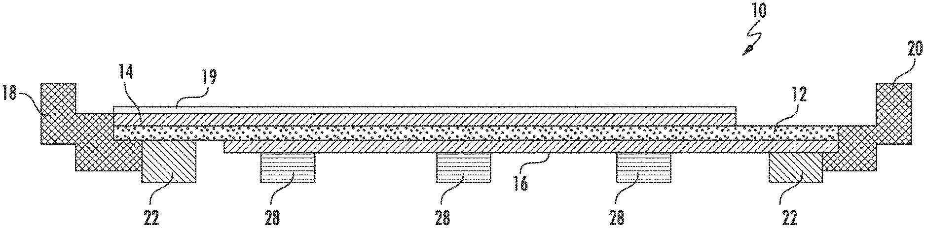
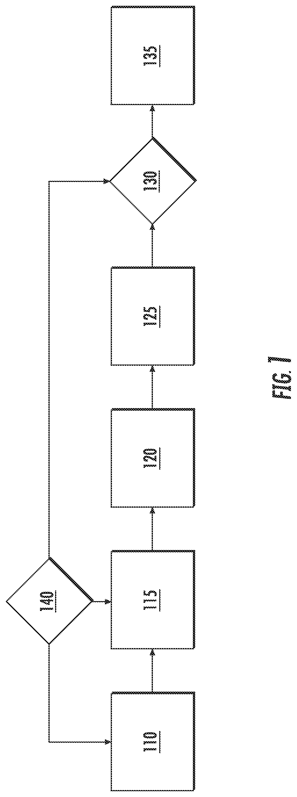
A method of making an electrocaloric is disclosed. The method includes: (a) providing a roll of a film comprising an electrocaloric material or a supply of multiple sheets of a film comprising an electrocaloric material; (b) delivering film from the roll or the supply of multiple sheets to a conductive material application station; (c) forming electrodes comprising a patterned disposition of conductive material on the film at the application station to form an electrocaloric article (d) delivering film from the application station to a take-up roll or an inventory of electrocaloric sheets; and (e) repeating (b), (c), and (d) to form multiple electrocaloric articles.
| Inventors: | Schmidt; Wayde R.; (Pomfret Center, CT) ; Culp; Slade R.; (Coventry, CT) ; Xie; Wei; (Manchester, CT) ; Mantese; Joseph V.; (Ellington, CT) ; Eastman; Scott Alan; (Glastonbury, CT) ; Annapragada; Subramanyaravi; (South Windsor, CT) ; Dardona; Sameh; (South Windsor, CT) ; Walker; Craig R.; (South Glastonbury, CT) ; Verma; Parmesh; (South Windsor, CT) | ||||||||||
| Applicant: |
|
||||||||||
|---|---|---|---|---|---|---|---|---|---|---|---|
| Family ID: | 62842313 | ||||||||||
| Appl. No.: | 16/623309 | ||||||||||
| Filed: | June 18, 2018 | ||||||||||
| PCT Filed: | June 18, 2018 | ||||||||||
| PCT NO: | PCT/US2018/038052 | ||||||||||
| 371 Date: | December 16, 2019 |
Related U.S. Patent Documents
| Application Number | Filing Date | Patent Number | ||
|---|---|---|---|---|
| 62521175 | Jun 16, 2017 | |||
| Current U.S. Class: | 1/1 |
| Current CPC Class: | F25B 2321/001 20130101; H01L 51/0076 20130101; H01L 37/02 20130101; F25B 41/00 20130101; H01L 25/04 20130101 |
| International Class: | H01L 37/02 20060101 H01L037/02; H01L 25/04 20060101 H01L025/04; F25B 41/00 20060101 F25B041/00 |
Claims
1. A method of making electrocaloric articles, comprising: (a) providing a roll of a film comprising an electrocaloric material or a supply of multiple sheets of a film comprising an electrocaloric material; (b) delivering film from the roll or the supply of multiple sheets to a conductive material application station; (c) forming electrodes comprising a patterned disposition of conductive material on the film at the application station to form an electrocaloric article (d) delivering film from the application station to a take-up roll or an inventory of electrocaloric sheets; and (e) repeating (b), (c), and (d) to form multiple electrocaloric articles.
2. The method of claim 1, wherein the patterned disposition of conductive material includes a power connection configured to connect to an electrical connection between a power source and the electrodes.
3. The method of claim 1, wherein forming electrodes at the application station comprises forming first and second electrodes on the same side of the film.
4. The method of claim 1, wherein forming electrodes at the application station comprises forming first and second electrodes on opposite sides of the film.
5. The method of claim 1, wherein forming electrodes at the application station comprises applying a patterned disposition of conductive material onto a temporary support and transferring the patterned disposition of conductive material from the temporary support to the film.
6. The method of claim 5, wherein forming the patterned disposition of conductive material to the temporary support comprises: (i) selectively applying conductive material to the temporary support, (ii) applying conductive material to the temporary support through a patterned mask, and removing the mask, (iii) selectively etching a conductive material on the temporary support, or (iv) applying conductive material to the temporary support, etching the conductive material through unmasked areas of a patterned mask, and removing the mask.
7. The method of claim 1, wherein forming the patterned disposition of conductive material comprises: (i) selectively applying conductive material to the film, (ii) applying conductive material to the film through a patterned mask, and removing the mask, (iii) selectively etching a conductive material on the film, or (iv) etching a conductive material on the film through unmasked areas of a patterned mask, and removing the mask.
8. The method of claim 6, wherein forming the patterned disposition of conductive material comprises selectively applying conductive material to the film or temporary support.
9. The method of claim 6, wherein forming the patterned disposition of conductive material comprises applying conductive material to the film or temporary support through a patterned mask, and removing the mask.
10. The method of claim 6, wherein forming the patterned disposition of conductive material comprises selectively etching a conductive material on the film or temporary support.
11. The method of claim 6, wherein forming the patterned disposition of conductive material comprises etching a conductive material on the film or temporary support through unmasked areas of a patterned mask, and removing the mask.
12. The method of claim 6, including applying conductive material includes ion implanted doping, ion implanted electrically active defects, or electron beam induced electrically active defects.
13. The method of claim 1, wherein forming the patterned disposition of conductive material includes cladding the electrocaloric material with an electrically conductive material.
14. The method of any of claim 1, wherein the patterned disposition of conductive material comprises a plurality of areas on the film surface comprising the conductive material separated by spacer areas on the film that do not comprise the conductive material.
15. The method of claim 14, wherein the plurality of areas on the electrocaloric film surface comprising the conductive material are configured as a plurality of electrically connected linear extensions of conductive material along the film surface separated by spacer areas.
16. The method of claim 7, wherein the plurality of areas on the electrocaloric film surface comprising the conductive material are spaced apart by a dimension of 0.1 times the film thickness to 10 times the film thickness.
17-18. (canceled)
19. The method of claim 1, further comprising disposing a protective layer over the electrode or electrodes comprising a patterned disposition of conductive material.
20. A method of making an electrocaloric module, comprising making an electrocaloric article according to claim 1, and disposing the electrocaloric article in an electrocaloric module comprising the electrocaloric article, a first thermal connection configured to connect to a first thermal flow path between the electrocaloric article and a heat sink, a second thermal connection configured to connect to a second thermal flow path between the electrocaloric article and a heat source, and a power connection connected to the electrodes and configured to connect to a power source.
21. The method of claim 20, further comprising disposing a plurality of the electrocaloric articles in electrocaloric module in a stack configuration.
22. A method of making an electrocaloric heat transfer system, comprising making an electrocaloric module according to claim 20 and connecting the first thermal c
D00000
D00001
D00002
D00003
D00004
D00005
D00006
D00007
XML
uspto.report is an independent third-party trademark research tool that is not affiliated, endorsed, or sponsored by the United States Patent and Trademark Office (USPTO) or any other governmental organization. The information provided by uspto.report is based on publicly available data at the time of writing and is intended for informational purposes only.
While we strive to provide accurate and up-to-date information, we do not guarantee the accuracy, completeness, reliability, or suitability of the information displayed on this site. The use of this site is at your own risk. Any reliance you place on such information is therefore strictly at your own risk.
All official trademark data, including owner information, should be verified by visiting the official USPTO website at www.uspto.gov. This site is not intended to replace professional legal advice and should not be used as a substitute for consulting with a legal professional who is knowledgeable about trademark law.