Short Wavelength Infrared Optoelectronic Devices Having A Dilute Nitride Layer
ROUCKA; RADEK ; et al.
U.S. patent application number 16/812668 was filed with the patent office on 2020-07-02 for short wavelength infrared optoelectronic devices having a dilute nitride layer. This patent application is currently assigned to ARRAY PHOTONICS, INC.. The applicant listed for this patent is ARRAY PHOTONICS, INC.. Invention is credited to TING LIU, AYMERIC MAROS, EVAN PICKETT, RADEK ROUCKA, SABEUR SIALA, FERRAN SUAREZ.
| Application Number | 20200212237 16/812668 |
| Document ID | / |
| Family ID | 63862207 |
| Filed Date | 2020-07-02 |


| United States Patent Application | 20200212237 |
| Kind Code | A1 |
| ROUCKA; RADEK ; et al. | July 2, 2020 |
SHORT WAVELENGTH INFRARED OPTOELECTRONIC DEVICES HAVING A DILUTE NITRIDE LAYER
Abstract
Semiconductor optoelectronic devices having a dilute nitride active layer are disclosed. In particular, the semiconductor devices have a dilute nitride active layer with a bandgap within a range from 0.7 eV and 1 eV. Photodetectors comprising a dilute nitride active layer have a responsivity of greater than 0.6 A/W at a wavelength of 1.3 .mu.m.
| Inventors: | ROUCKA; RADEK; (EAST PALO ALTO, CA) ; SIALA; SABEUR; (SUNNYVALE, CA) ; MAROS; AYMERIC; (SAN FRANCISCO, CA) ; LIU; TING; (SAN JOSE, CA) ; SUAREZ; FERRAN; (CHANDLER, AZ) ; PICKETT; EVAN; (MENLO PARK, CA) | ||||||||||
| Applicant: |
|
||||||||||
|---|---|---|---|---|---|---|---|---|---|---|---|
| Assignee: | ARRAY PHOTONICS, INC. TEMPE AZ |
||||||||||
| Family ID: | 63862207 | ||||||||||
| Appl. No.: | 16/812668 | ||||||||||
| Filed: | March 9, 2020 |
Related U.S. Patent Documents
| Application Number | Filing Date | Patent Number | ||
|---|---|---|---|---|
| PCT/US2018/052873 | Sep 26, 2018 | |||
| 16812668 | ||||
| 62564124 | Sep 27, 2017 | |||
| Current U.S. Class: | 1/1 |
| Current CPC Class: | H01L 31/03046 20130101; H01L 33/007 20130101; H01L 33/0075 20130101; H01L 31/107 20130101; H01L 31/1844 20130101; H01L 33/32 20130101; H01L 33/30 20130101; H01L 31/03048 20130101; H01L 27/1446 20130101; H01L 31/105 20130101 |
| International Class: | H01L 31/0304 20060101 H01L031/0304; H01L 33/30 20060101 H01L033/30; H01L 31/18 20060101 H01L031/18; H01L 27/144 20060101 H01L027/144 |
Claims
1. A compound semiconductor optoelectronic device, comprising: a substrate; a first doped III-V layer overlying the substrate; an active region overlying the first doped III-V region, wherein, the active region comprises a lattice matched dilute nitride layer or a pseudomorphic dilute nitride layer; the dilute nitride layer has a bandgap within a range from 0.7 eV and 1.0 eV; and the dilute nitride layer has a minority carrier lifetime of 1 ns or greater at a temperature of 25.degree. C.; and a second doped III-V layer overlying the active region.
2. The device of claim 1, wherein the dilute nitride layer has a compressive strain within a range from 0% and 0.4% with respect to the substrate.
3. The device of claim 1, wherein the dilute nitride layer has a minority carrier lifetime of 2 ns or greater.
4. The device of claim 1, wherein the substrate comprises GaAs, AlGaAs, Ge, SiGeSn, or buffered Si.
5. The device of claim 1, wherein the dilute nitride layer has a lattice constant less than 3% the lattice constant of GaAs or Ge.
6. The device of claim 1, wherein the dilute nitride layer comprises GaInNAs, GaNAsSb, GaInNAsSb, GaInNAsBi, GaNAsSbBi, GaNAsBi, or GaInNAsSbBi.
7. The device of claim 1, wherein the dilute nitride layer comprises Ga.sub.1-xIn.sub.xN.sub.yAs.sub.1-y-zSb.sub.z, wherein 0.ltoreq.x.ltoreq.0.4, 0<y.ltoreq.0.07, and 0<z.ltoreq.0.04.
8. The device of claim 1, wherein the dilute nitride layer comprises Ga.sub.1-xIn.sub.xN.sub.yAs.sub.1-y-zSb.sub.z, wherein 0.12.ltoreq.x.ltoreq.0.24, 0.03.ltoreq.y.ltoreq.0.07 and 0.001.ltoreq.z.ltoreq.0.02; 0.12.ltoreq.x.ltoreq.0.24, 0.03.ltoreq.y.ltoreq.0.07, and 0.005.ltoreq.z.ltoreq.0.04; 0.13.ltoreq.x.ltoreq.0.20, 0.03.ltoreq.y.ltoreq.0.045 and 0.001.ltoreq.z.ltoreq.0.02; 0.13.ltoreq.x.ltoreq.0.18, 0.03.ltoreq.y.ltoreq.0.04 and 0.001.ltoreq.z.ltoreq.0.02; or 0.18.ltoreq.x.ltoreq.0.24, 0.04.ltoreq.y.ltoreq.0.07 and 0.01.ltoreq.z.ltoreq.0.04.
9. The device of claim 1, wherein the dilute nitride layer has a thickness within a range from 0.2 .mu.m to 10 .mu.m.
10. The device of claim 1, wherein the device comprises a photodetector.
11. The device of claim 10, wherein the photodetector has a responsivity greater than 0.6 A/W at 1300 nm.
12. The device of claim 10, wherein the photodetector has a responsivity greater than 0.8 A/W at 1300 nm.
13. The device of claim 1, wherein the device comprises a light emitting diode.
14. A method of forming a semiconductor optoelectronic device, comprising: forming a substrate; forming a first doped III-V layer overlying the substrate; forming an active region overlying the first doped III-V layer, wherein, the active region comprises a pseudomorphic dilute nitride layer; the dilute nitride layer has a bandgap within a range from 0.7 eV and 1.0 eV; and the dilute nitride layer has a minority carrier lifetime of 1 ns or greater; and forming a second doped III-V layer overlying the active region.
15. The method of claim 14, wherein the dilute nitride layer comprises GaInNAs, GaNAsSb, GaInNAsSb, GaInNAsBi, GaNAsSbBi, GaNAsBi, or GaInNAsSbBi.
16. The method of claim 14, wherein the dilute nitride layer comprises Ga.sub.1-xIn.sub.xN.sub.yAs.sub.1-y-zSb.sub.z, wherein 0.ltoreq.x.ltoreq.0.4, 0<y.ltoreq.0.07, and 0<z.ltoreq.0.04.
17. The method of claim 14, wherein the dilute nitride layer comprises Ga.sub.1-xIn.sub.xN.sub.yAs.sub.1-y-zSb.sub.z, wherein 0.12.ltoreq.x.ltoreq.0.24, 0.03.ltoreq.y.ltoreq.0.07 and 0.001.ltoreq.z.ltoreq.0.02; 0.12.ltoreq.x.ltoreq.0.24, 0.03.ltoreq.y.ltoreq.0.07, and 0.005<z.ltoreq.0.04; 0.13.ltoreq.x.ltoreq.0.2, 0.03.ltoreq.y.ltoreq.0.045 and 0.001.ltoreq.z.ltoreq.0.02; 0.13.ltoreq.x.ltoreq.0.18, 0.03.ltoreq.y.ltoreq.0.04 and 0.001.ltoreq.z.ltoreq.0.02; or 0.18.ltoreq.x.ltoreq.0.24, 0.04.ltoreq.y.ltoreq.0.07 and 0.01.ltoreq.z.ltoreq.0.04.
18. The method of claim 14, wherein the dilute nitride layer has a thickness within a range from 0.2 .mu.m and 10 .mu.m.
19. The method of claim 14, wherein the substrate comprises GaAs, AlGaAs, Ge, SiGeSn, or buffered Si.
20. The method of claim 14, wherein the dilute nitride layer has a lattice constant less than 3% the lattice constant of GaAs or Ge.
21. The method of claim 14, wherein the dilute nitride layer has a compressive strain within a range from 0% and 0.4% with respect to the substrate.
22. The method of claim 14, wherein the device comprises a photodetector.
23. The method of claim 21, wherein the photodetector has a responsivity greater than 0.6 A/W at 1300 nm.
24. The method of claim 21, wherein the photodetector has a responsivity greater than 0.8 A/W at 1300 nm.
Description
[0001] This application is a continuation under 35 U.S.C. .sctn. 111(a) of PCT International Application No. PCT/US2018/052873 filed on Sep. 26, 2018, which claims the benefit under 35 U.S.C. .sctn. 119(e) of U.S. Provisional Application No. 62/564,124, filed on Sep. 27, 2017, which is incorporated by reference in its entirety.
FIELD
[0002] The disclosure relates to shortwave infrared (SWIR) optoelectronic devices operating within the wavelength range of 0.9 .mu.m to 1.8 .mu.m including photodetectors and photodetector arrays.
BACKGROUND
[0003] Optoelectronic devices operating in the infrared wavelength range between 0.9 .mu.m and 1.8 .mu.m range have a wide range of applications, including fiber optic communications, sensing and imaging. Traditionally, compound III-V semiconductor materials are used to make such devices. Indium gallium arsenide (InGaAs) materials are usually grown on indium phosphide (InP) substrates. The composition and thickness of the InGaAs layers are chosen to provide the required functionality, such as light emission or absorption at desired wavelengths of light and are also lattice-matched or very closely lattice-matched to the InP substrate, in order to produce high quality materials that have low levels of crystalline defects, and high levels of performance.
[0004] With respect to photodetectors, devices that can be produced include high-speed photodetectors for telecommunications applications, and arrays of photodetectors that can be used as sensors and imagers for military, biomedical, industrial, environmental and scientific applications. In such applications, photodetectors with high responsivity, low dark current and low noise are desirable.
[0005] Although InGaAs on InP materials currently dominate the short wavelength infrared (SWIR) photodetector market, the material system has several limitations, including the high cost of InP substrates, low yields due to fragility of the InP substrates, and limited InP wafer diameter (and associated quality issues at larger diameters). From a manufacturing perspective, and also an economic perspective, gallium arsenide (GaAs) represents a better substrate choice. However, the large lattice mismatch between GaAs and the InGaAs alloys required for infrared devices produces poor quality materials that compromise electrical and optical performance. Attempts have been made to produce long-wavelength (greater than 1.2 .mu.m) materials for photodetectors on GaAs based on dilute nitride materials such as GaInNAs and GaInNAsSb. However, where device performance is reported, it has been much poorer than for InGaAs/InP devices, for example, the dilute nitride-based devices have very low responsivity, which make the devices unsuited for practical sensing and photodetection applications. Other considerations for photodetectors include dark current, and specific responsivity.
[0006] For example, Cheah et al., "GaAs-Based Heterojunction p-i-n Photodetectors Using Pentenary InGaAsNSb as the Intrinsic Layer", IEEE Photon. Technol. Letts., 17(9), pp. 1932-1934 (2005), and Loke et al., "Improvement of GaInNAs p-i-n photodetector responsivity by antimony incorporation", J. Appl. Phys. 101, 033122 (2007) report photodetectors having a responsivity of only 0.097 A/W at a wavelength of 1300 nm.
[0007] Tan et al., "GaInNAsSb/GaAs Photodiodes for Long Wavelength Applications, IEEE Electron. Dev. Letts., 32(7), pp. 919-921 (2011) describe photodiodes having a responsivity of only 0.18 A/W at a wavelength of 1300 nm.
[0008] In U.S. Application Publication No. 2016/0372624, Yanka et al. disclose optoelectronic detectors having dilute nitride layers (InGaNAsSb). Although certain parameters that relate to semiconductor material quality are described, no working detectors having practical efficiencies are taught within the broad compositional range disclosed.
[0009] Thus, to take advantage of the manufacturing scalability and cost advantages of GaAs substrates, there is continued interest in developing long-wavelength materials on GaAs that have improved optoelectronic performance.
SUMMARY
[0010] According to the present invention compound semiconductor optoelectronic devices comprise a substrate; a first doped III-V layer overlying the substrate; an active region overlying the first doped III-V region, wherein, the active region comprises a lattice matched or pseudomorphic dilute nitride layer; and the dilute nitride layer has a bandgap within a range from 0.7 eV and 1.0 eV; and a second doped III-V layer overlying the active region.
[0011] According to the present invention, methods of forming a semiconductor optoelectronic device comprise forming a substrate; forming a first doped III-V layer overlying the substrate; forming an active region overlying the first doped III-V layer, wherein, the active region comprises a pseudomorphic dilute nitride layer; and the dilute nitride layer has a bandgap within a range from 0.7 eV and 1.0 eV; and forming a second doped III-V layer overlying the active region.
BRIEF DESCRIPTION OF THE DRAWINGS
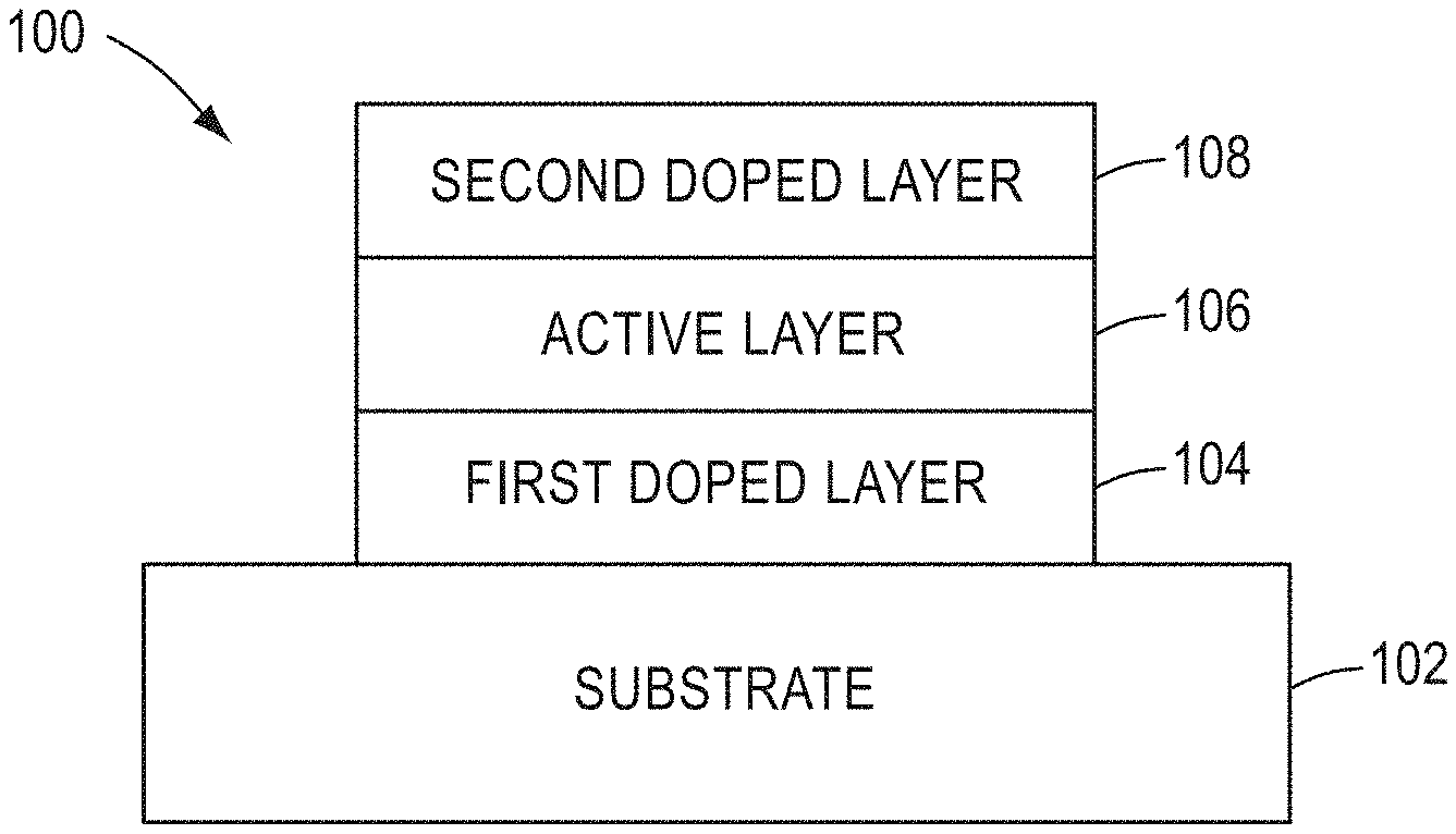
[0012] The drawings described herein are for illustration purposes only. The drawings are not intended to limit the scope of the present disclosure.
[0013] FIG. 1 shows a side view of an example of a semiconductor optoelectronic device according to the present invention.
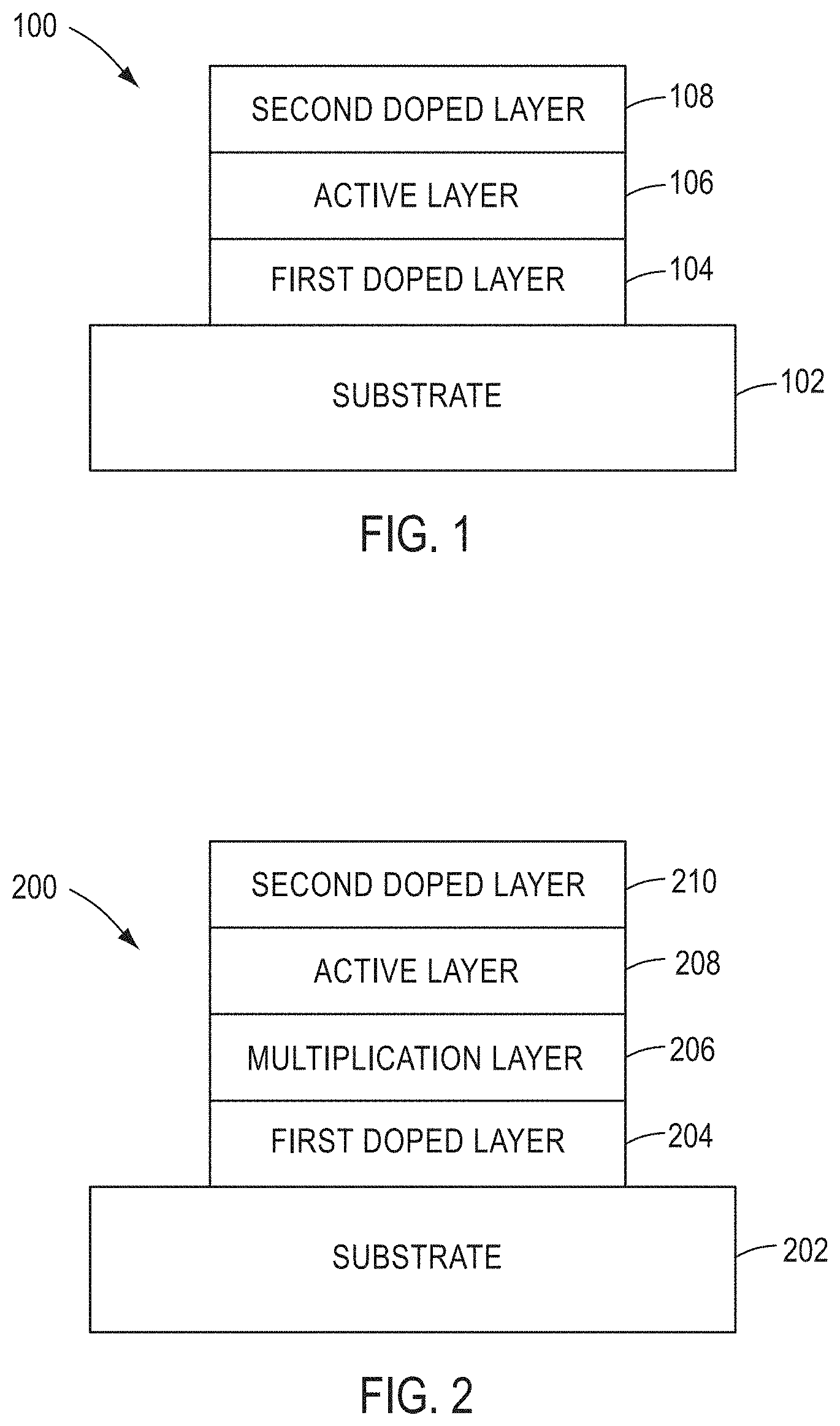
[0014] FIG. 2 shows a side view of another example of a semiconductor optoelectronic device according to the present invention.
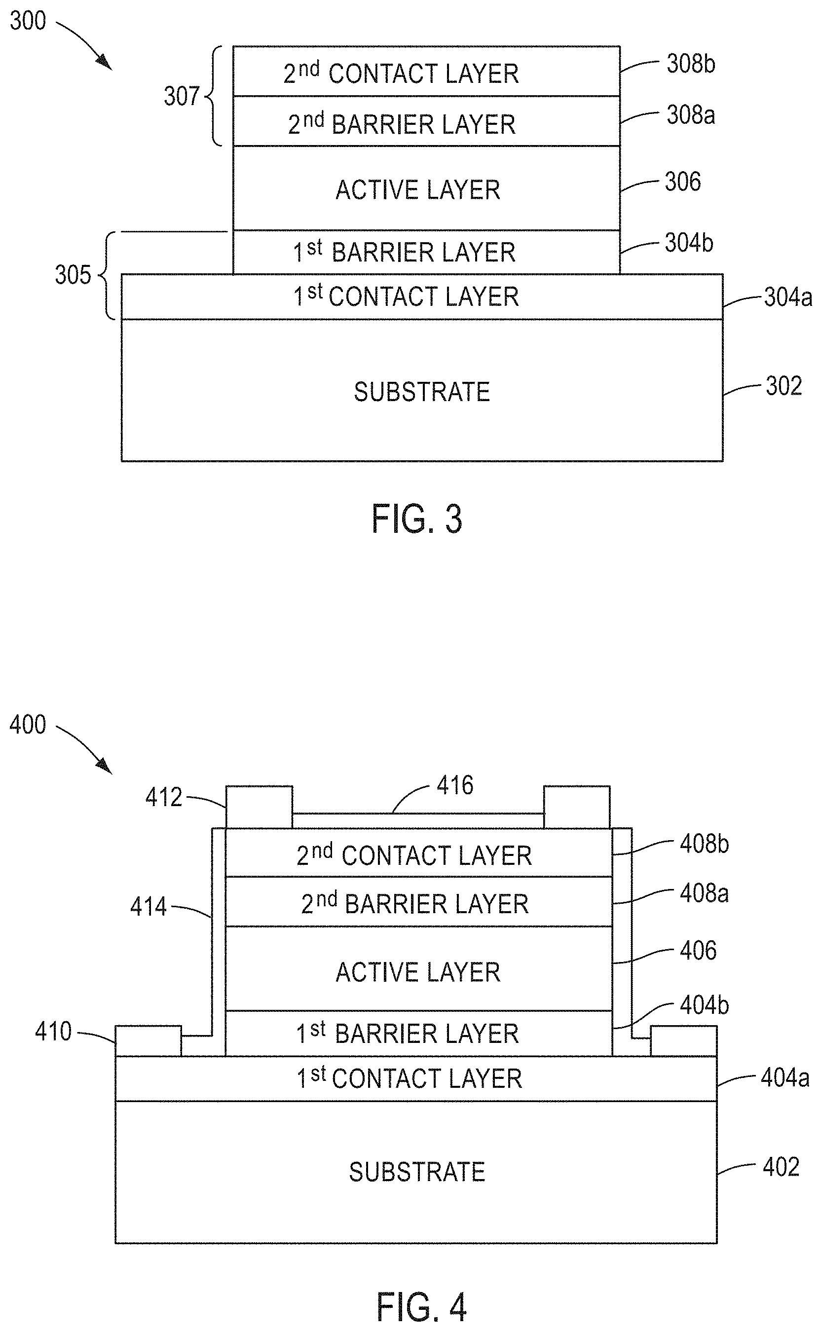
[0015] FIG. 3 shows a side view of another example of a semiconductor optoelectronic device according to the present invention.
[0016] FIG. 4 shows a side view of an example of a photodetector according to the present invention.
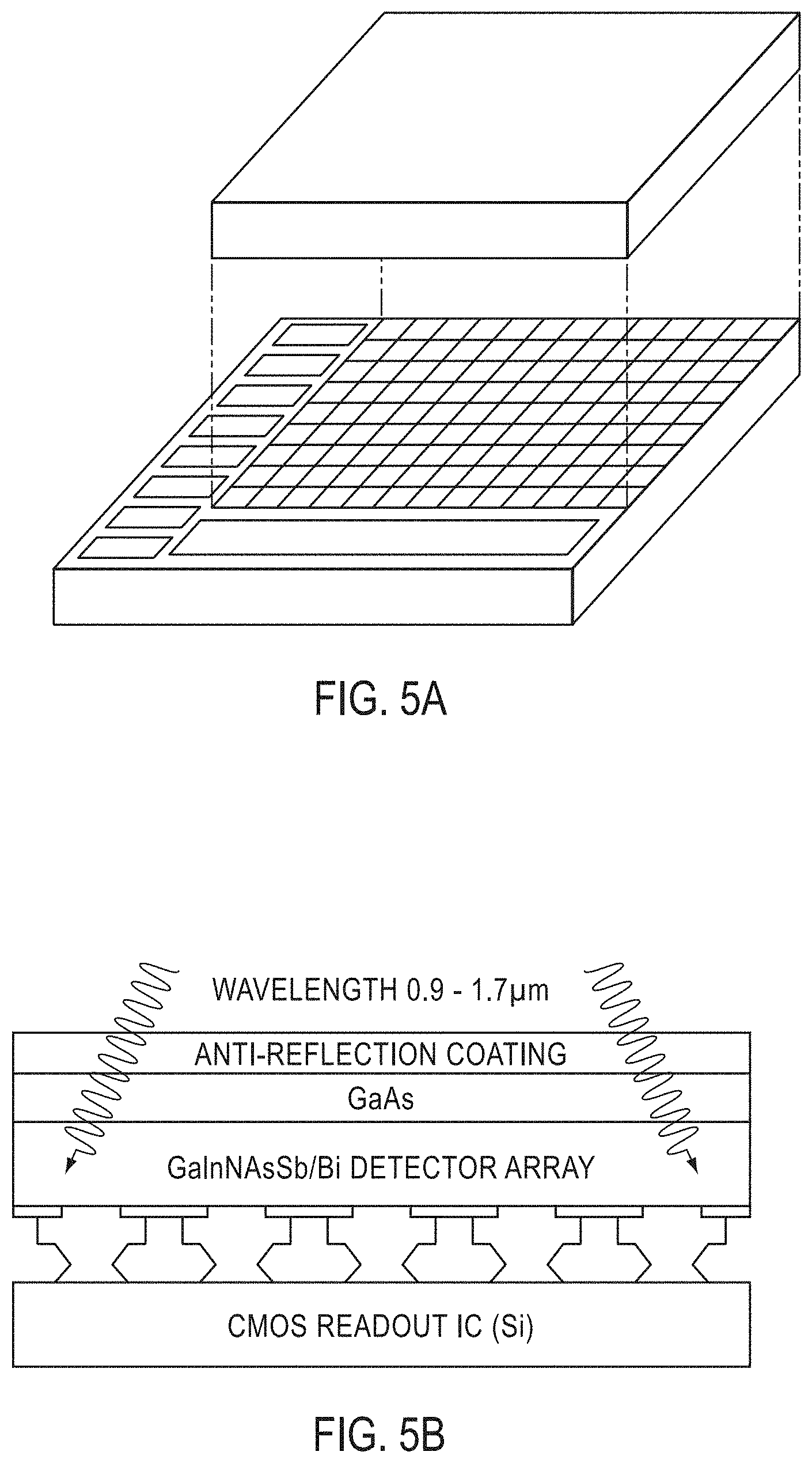
[0017] FIGS. 5A and 5B are diagrams showing hybrid integration of a detector array chip with an array of readout circuits on a readout integrated circuit (ROIC) chip
[0018] FIG. 6 shows an X-ray diffraction scan of a GaInNAsSb dilute nitride layer formed on a GaAs substrate according to the present invention.
[0019] FIG. 7 shows an X-ray diffraction scan of another GaInNAsSb dilute nitride layer formed on a GaAs substrate according to the present invention.
[0020] FIG. 8 shows a photoluminescence spectrum for a GaInNAsSb layer grown on a GaAs substrate according to the present invention.
[0021] FIG. 9 shows a photoluminescence spectrum for another GaInNAsSb layer grown on a GaAs substrate according to the present invention.
[0022] FIG. 10 shows a photoluminescence spectrum for another GaInNAsSb layer grown on a GaAs substrate according to the present invention.
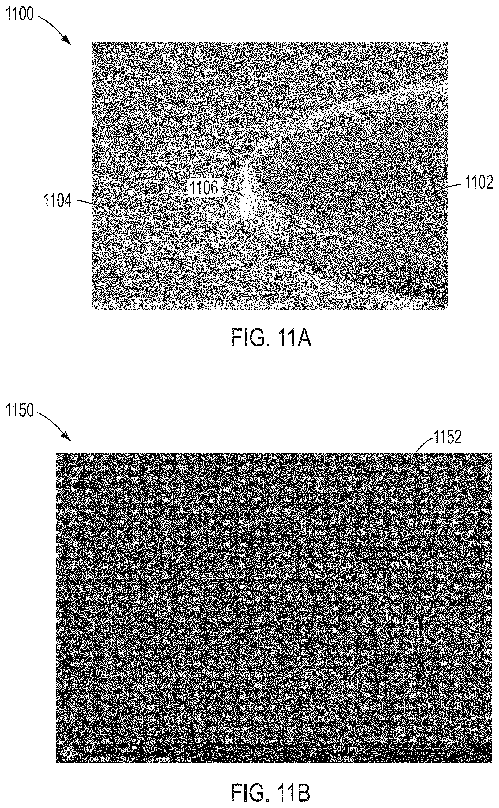
[0023] FIG. 11A shows a scanning electron microscopy (SEM) image of an etched mesa for a GaInNAsSb dilute nitride photodetector.
[0024] FIG. 11B shows a scanning electron microscopy image of an array of photodetectors according to the present invention.
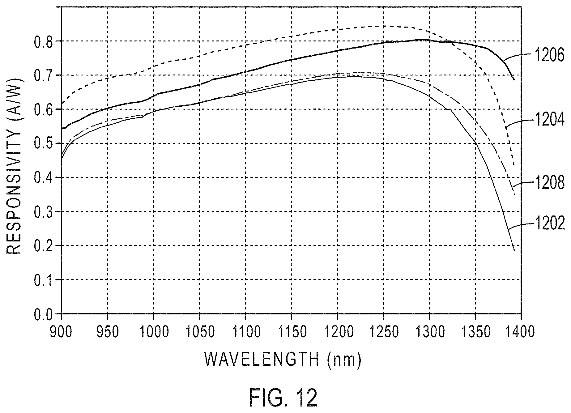
[0025] FIG. 12. shows measured responsivity curves for photodetectors according to the present invention.
[0026] FIG. 13A shows a schematic of a device having II-V semiconductor layers grown on a GaAs substrate.
[0027] FIG. 13B shows a schematic of a device having II-V semiconductor layers grown on a Ge substrate.
[0028] FIG. 14A shows a semiconductor device having a lattice engineered SiGe buffer layer over a silicon substrate.
[0029] FIG. 14B shows a semiconductor device having a lattice engineered SiGeSn buffer layer over a silicon substrate.
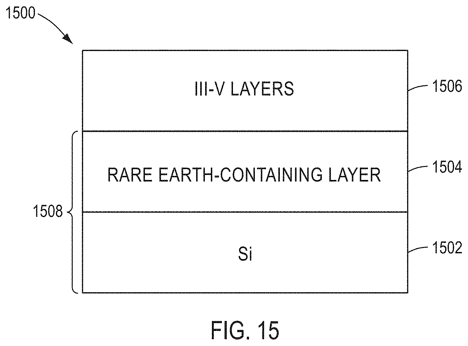
[0030] FIG. 15 shows a semiconductor device having a lattice engineered rare earth-containing buffer layer over a silicon substrate.
DETAILED DESCRIPTION
[0031] The following detailed description refers to the accompanying drawings that show, by way of illustration, specific details and embodiments in which the invention may be practiced. These embodiments are described in sufficient detail to enable those skilled in the art to practice the present invention. Other embodiments may be utilized and structural, logical, and electrical changes may be made without departing from the scope of the invention. The various embodiments disclosed herein are not necessarily mutually exclusive, as some disclosed embodiments may be combined with one or more other disclosed embodiments to form new embodiments. The following detailed description is, therefore, not to be taken in a limiting sense, and the scope of the embodiments of the present invention is defined only by the appended claims, along with the full scope of equivalents to which such claims are entitled.
[0032] The term "lattice matched" as used herein means that the two referenced materials have the same lattice constant or a lattice constant differing by less than +/-0.2%. For example, GaAs and AlAs are lattice matched, having lattice constants differing by 0.12%.
[0033] The term "pseudomorphically strained" as used herein means that layers made of different materials with a lattice constant difference up to +/-2% can be grown on top of a lattice matched or strained layer without generating misfit dislocations. The lattice parameters can differ, for example, by up to +/-1%, by up to +/-0.5%, or by up to +/-0.2%.
[0034] The term "layer" as used herein, means a continuous region of a material (e.g., an alloy) that can be uniformly or non-uniformly doped and that can have a uniform or a non-uniform composition across the region.
[0035] The term "bandgap" as used herein is the energy difference between the conduction and valence bands of a material.
[0036] The term responsivity of a material as used herein is the ratio of the generated photocurrent to the incident light power at a given wavelength.
[0037] FIG. 1 shows a side view of an example of a semiconductor optoelectronic device 100 according to the present invention. Device 100 comprises a substrate 102, a first doped layer 104, an active layer 106, and a second doped layer 108. For simplicity, each layer is shown as a single layer. However, it will be understood that each layer can include one or more layers with differing compositions, thicknesses, and doping levels to provide an appropriate optical and/or electrical functionality, and to improve interface quality, electron transport, hole transport and/or other optoelectronic properties.
[0038] Substrate 102 can have a lattice constant that matches or nearly matches the lattice constant of GaAs or Ge. The substrate can be GaAs. Substrate 102 may be doped p-type, or n-type, or may be a semi-insulating (SI) substrate. The thickness of substrate 102 can be chosen to be any suitable thickness. Substrate 102 can include one or more layers, for example, the substrate can include a Si layer having an overlying SiGeSn buffer layer, a rare-earth containing layer, or a graded SiGe layer that is engineered to have a lattice constant that matches or nearly matches the lattice constant of GaAs or Ge. A material such as a substrate having a lattice constant that nearly matches the lattice constant of GaAs or Ge means that the material such as the substrate has a lattice constant different than that of GaAs or Ge by less than or equal to 3%, less than 1%, or less than 0.5% of the lattice constant of GaAs or Ge.
[0039] First doped layer 104 can have a doping of one type and the second doped layer 108 can have a doping of the opposite type. If first doped layer 104 is doped n-type, second doped layer 108 is doped p-type. Conversely, if first doped layer 104 is doped p-type, second doped layer 108 is doped n-type. Examples of p-type dopants include C and Be. Examples of n-type dopants include Si and Te. Doped layers 104 and 108 are chosen to have a composition that is lattice matched or pseudomorphically strained to the substrate. The doped layers can comprise any suitable III-V material, such as GaAs, AlGaAs, GaInAs, GaInP, GaInPAs, GaInNAs, or GaInNAsSb. The bandgap of the doped layers can be selected to be larger than the bandgap of active layer 106. Doping levels can be within a range, for example, from 1.times.10.sup.15 cm.sup.-3 to 2.times.10.sup.19 cm.sup.-3. Doping levels may be constant within a layer, and/or the doping profile may be graded, for example, the doping level can increase from a minimum value to a maximum value as a function of the distance from the interface between the first doped layer 104 and the active layer 106. Doped layers 104 and 108 can have a thickness within a range, for example, from 50 nm to 3 .mu.m.
[0040] Active layer 106 can be lattice matched or pseudomorphically strained with respect to the substrate and/or to the doped layers. The bandgap of active layer 106 can be lower than that of the doped layers 104 and 108. Active layer 106 comprises a layer capable of processing light over a desired wavelength range. Processing is defined to be a light emission, a light receiving, a light sensing and light modulation.
[0041] Active layer 106 can include a dilute nitride material. A dilute nitride material can be Ga.sub.1-xIn.sub.xN.sub.yAs.sub.1-y-zSb.sub.z, where x, y and z can be 0.ltoreq.x.ltoreq.0.4, 0<y.ltoreq.0.07 and 0<z.ltoreq.0.04, respectively. X, y and z can be 0.01.ltoreq.x.ltoreq.0.4, 0.02.ltoreq.y.ltoreq.0.07 and 0.001.ltoreq.z.ltoreq.0.04, respectively. In other embodiments, dilute nitride materials can have compositions as disclosed in U.S. Pat. No. 8,962,993, where x, y and z can be 0.ltoreq.x.ltoreq.0.24, 0.02.ltoreq.y.ltoreq.0.05 and 0.001.ltoreq.z.ltoreq.0.2, respectively. A dilute nitride material can be Ga.sub.1-xIn.sub.xN.sub.yAs.sub.1-y-zSb.sub.z, where, for example, 0.12.ltoreq.x.ltoreq.0.24, 0.03.ltoreq.y.ltoreq.0.07 and 0.005.ltoreq.z.ltoreq.0.04; 0.13.ltoreq.x.ltoreq.0.2, 0.03.ltoreq.y.ltoreq.0.045 and 0.001.ltoreq.z.ltoreq.0.02; 0.13.ltoreq.x.ltoreq.0.18, 0.03.ltoreq.y.ltoreq.0.04 and 0.001.ltoreq.z.ltoreq.0.02; or 0.18.ltoreq.x.ltoreq.0.24, 0.04.ltoreq.y.ltoreq.0.07 and 0.01.ltoreq.z.ltoreq.0.024. Active layer 106 can have a bandgap within a range from 0.7 eV and 1.1 eV such that the active layer can absorb or emit light at wavelengths up to 1.8 .mu.m. Bismuth (Bi) may be added as a surfactant during growth of the dilute nitride material, improving material quality (such as defect density), and the device performance. The thickness of active layer 106 can be within a range, for example, from 0.2 .mu.m to 10 .mu.m. The thickness of active layer 106 can be within a range, for example, from 0.5 .mu.m to 5 .mu.m. The thickness of active layer 106 can be within a range, for example, from 1 .mu.m to 4 .mu.m, from 1 .mu.m to 3 .mu.m, or from 1 .mu.m to 2 .mu.m. Active layer 106 can be compressively strained with respect to the substrate 102. Strain can improve device performance. For a photodetector, the parameters most relevant to device performance include the dark current, operating speed, noise, and responsivity.
[0042] Active layer 106 and doped layers 104 and 108 form a p-i-n or an n-i-p junction. This junction provides the basic structure for operation of a device such as a photodetector or a light-emitting diode. For photodetectors, p-i-n epitaxial structures can have low background doping in the intrinsic region (active layer) of the devices which are typically operated at 0 V or very low bias. Therefore, the active layer 106 may not be deliberately doped. The active layer can be an intrinsic layer or an unintentionally doped layer. Unintentionally doped semiconductors do not have dopants intentionally added but can include a nonzero concentration of impurities that act as dopants. The background carrier concentration of the intrinsic or unintentionally doped active layer, which is equivalent to the dopant concentration, can be, for example, less than 1.times.10.sup.16 cm.sup.-3 (measured at room temperature (25.degree. C.), less than 5.times.10.sup.15 cm.sup.-3, or less than 1.times.10.sup.15 cm.sup.-3. The minority carrier lifetime within the active layer can be, for example, greater than 1 ns, greater than 1.5 ns, or greater 2 ns. The minority carrier lifetime can be affected by defects within the semiconductor that contribute to the background carrier concentration, as well as other defect types that can act as recombination centers but do not contribute carriers.
[0043] FIG. 2 shows a semiconductor optoelectronic device 200 with a p-i-n diode and a multiplication layer. Device 200 is similar to device 100, but also includes a multiplication layer. The purpose of the multiplication layer is to amplify the photocurrent generated by the active region of a photodetector device. The structure of device 200 can provide an avalanche photodiode (APD). An APD introduces an additional p-n junction into the structure, as well as introduces an additional thickness. This allows a higher reverse bias voltage to be applied to the device, which results in carrier multiplication by the avalanche process.
[0044] Substrate 202 can have a lattice constant that matches or nearly matches the lattice constant of GaAs or Ge. The substrate can be GaAs. Substrate 202 may be doped p-type, or n-type, or may be a semi-insulating (SI) substrate. The thickness of substrate 202 can be chosen to be any suitable thickness. Substrate 202 can include one or more layers, for example, a Si layer having an overlying SiGeSn buffer layer that is engineered to have a lattice constant that matches or nearly matches the lattice constant of GaAs or Ge. This can mean the substrate has a lattice parameter different than that of GaAs or Ge by less than or equal to 3%, less than 1%, or less than 0.5% that of GaAs or Ge.
[0045] First doped layer 204 can have a doping of one type and the second doped layer 210 can have a doping of the opposite type. If first doped layer 204 is doped n-type, second doped layer 210 is doped p-type. Conversely, if first doped layer 204 is doped p-type, second doped layer 210 is doped n-type. Examples of p-type dopants include C and Be. Examples of n-type dopants include Si and Te. Doped layers 204 and 210 can be chosen to have a composition that is lattice matched or pseudomorphically strained to the substrate. The doped layers can comprise any suitable III-V material, such as GaAs, AlGaAs, GaInAs, GaInP, GaInPAs, GaInNAs, GaInNAsSb. The bandgap of the doped layers can be selected to be larger than the bandgap of active layer 208. Doping levels can be within a range, for example, from 1.times.10.sup.15 cm.sup.-3 to 2.times.10.sup.19 cm.sup.-3. Doping levels may be constant within a layer and/or the doping profile may be graded, for example, the doping level can increase from a minimum value to a maximum value as a function of the distance from the interface between the second doped layer 210 and the active layer 208. Doped layers 204 and 210 can have a thickness, for example, within a range from 50 nm and 3 .mu.m.
[0046] Active layer 208 can be lattice matched or pseudomorphically strained to the substrate and/or to the doped layers. The bandgap of active layer 208 can be lower than that of the doped layers 204 and 210. Active layer 208 can comprise a layer capable of processing light over a desired wavelength range. Processing is defined to be a light emission, a light receiving, a light sensing and light modulation.
[0047] Active layer 208 can include a dilute nitride material. The dilute nitride material can be Ga.sub.1-xIn.sub.xN.sub.yAs.sub.1-y-zSb.sub.z, where x, y and z can be 0.ltoreq.x.ltoreq.0.4, 0<y.ltoreq.0.07 and 0<z.ltoreq.0.04, respectively. X, y and z can be 0.01.ltoreq.x.ltoreq.0.4, 0.02.ltoreq.y.ltoreq.0.07 and 0.001.ltoreq.z.ltoreq.0.04, respectively. In other embodiments, dilute nitride materials can have compositions as disclosed in U.S. Pat. No. 8,962,993, where x, y and z can be 0.ltoreq.x.ltoreq.0.24, 0.02.ltoreq.y.ltoreq.0.05 and 0.001.ltoreq.z.ltoreq.0.2, respectively. A dilute nitride material can be Ga.sub.1-xIn.sub.xN.sub.yAs.sub.1-y-zSb.sub.z, where, for example, 0.12.ltoreq.x.ltoreq.0.24, 0.03.ltoreq.y.ltoreq.0.07 and 0.005.ltoreq.z.ltoreq.0.04; 0.13.ltoreq.x.ltoreq.0.20, 0.03.ltoreq.y.ltoreq.0.045 and 0.001.ltoreq.z.ltoreq.0.02; 0.13.ltoreq.x.ltoreq.0.18, 0.03.ltoreq.y.ltoreq.0.04 and 0.001.ltoreq.z.ltoreq.0.02; or 0.18.ltoreq.x.ltoreq.0.24, 0.04.ltoreq.y.ltoreq.0.07 and 0.01.ltoreq.z.ltoreq.0.04. Active layer 208 can have a bandgap within a range from 0.7 eV to 1.1 eV such that the active layer can absorb or emit light at wavelengths up to 1.8 .mu.m. Bismuth (Bi) may be added as a surfactant during growth of the dilute nitride, improving material quality (such as defect density), and the device performance. The thickness of active layer 208 can be within a range, for example, from 0.2 .mu.m to 10 .mu.m, from 0.5 .mu.m to 5 .mu.m, or from 1 .mu.m to 4 .mu.m. Active layer 208 can be compressively strained with respect to the substrate 202. Strain can also improve device performance. For a photodetector, the device performance of most relevance includes the dark current, operating speed, noise and responsivity.
[0048] The multiplication layer 206 can be a p-type III-V layer configured to amplify the current generated by the active layer 208 through avalanche multiplication. Thus, for each free carrier (electron or hole) generated by the active layer 208, the multiplication layer 206 generates one or more carriers via the avalanche effect. Thus, the multiplication layer 206 increases the total current generated by the semiconductor 200. Multiplication layer 206 can comprise a III-V material, such as GaAs or AlGaAs.
[0049] FIG. 3 shows a side view of an example of a semiconductor optoelectronic device 300 according to the present invention. Device 300 is similar to device 100, but each of the doped layers are shown to comprise two layers. Device 300 includes a substrate 302, a first contact layer 304a, a first barrier layer 304b, an active layer 306, a second barrier layer 308a, and a second contact layer 308b.
[0050] Substrate 302 can have a lattice constant that matches or nearly matches the lattice constant of GaAs or Ge. The substrate can be GaAs. Substrate 302 may be doped p-type, or n-type, or may be a semi-insulating (SI substrate). The thickness of substrate 302 can be any suitable thickness. Substrate 302 can include one or more layers, for example, substrate 302 can include a Si layer having an overlying SiGeSn buffer layer that is engineered to have a lattice constant that matches or nearly matches the lattice constant of GaAs or Ge. This can mean that the substrate can have a lattice parameter different than that of GaAs or Ge by less than or equal to 3%, less than 1%, or less than 0.5% that of GaAs or Ge.
[0051] First contact layer 304a and first barrier layer 304b provide a first doped layer 305, having a doping of one type, and second barrier layer 308a and second contact layer 308b provide a second doped layer 307, having a doping of the opposite type. If first doped layer 305 is doped n-type, second doped layer 307 is doped p-type. Conversely, if first doped layer 305 is doped p-type, second doped layer 307 is doped n-type. Examples of p-type dopants include C and Be. Examples of n-type dopants include Si and Te. Doped layers 305 and 307 can be chosen to have a composition that is lattice matched or pseudomorphically strained with respect to the substrate. The doped layers can comprise any suitable III-V material, such as GaAs, AlGaAs, GaInAs, GaInP, GaInPAs, GaInNAs, GaInNAsSb. The contact and barrier layers can have different compositions and different thicknesses. The bandgap of the doped layers can be selected to be larger than the bandgap of active region 306. The doping level of first contact layer 304a can be chosen to be higher than the doping level of first barrier layer 304b. A higher doping facilitates electrical connection with a metal contact. Similarly, the doping level of second contact layer 304b can be chosen to be higher than the doping level of second barrier layer 304a. Higher doping levels facilitate electrical connection with a metal contact. Doping levels can be within a range, for example, from 1.times.10.sup.15 cm.sup.-3 to 2.times.10.sup.19 cm.sup.-3. Doping levels may be constant within a layer and/or the doping profile may be graded, for example, the doping level can increase from a minimum value to a maximum value as a function of the distance from the interface between the doped layer 308a and the active layer 306. Each of barrier and contact layers 304a, 304b, 308a and 308b can have a thickness, for example, within a range from 50 nm to 3 .mu.m.
[0052] Active layer 306 can be lattice matched or pseudomorphically strained to the substrate and/or to the barrier layers. The bandgap of active layer 306 can be lower than that of barrier and contact layers 304a, 304b, 308a and 308b. Active layer 306 can comprise a layer capable of processing light over a desired wavelength range. Processing is defined to be a light emission, a light receiving, a light sensing and light modulation.
[0053] Active layer 306 can include a dilute nitride material. The dilute nitride material can be Ga.sub.1-xIn.sub.xN.sub.yAs.sub.1-y-zSb.sub.z, where x, y and z can be 0.ltoreq.x.ltoreq.0.4, 0<y.ltoreq.0.07 and 0<z.ltoreq.0.04, respectively. X, y and z can be 0.01.ltoreq.x.ltoreq.0.4, 0.02.ltoreq.y.ltoreq.0.07 and 0.001.ltoreq.z.ltoreq.0.04, respectively. In other embodiments, dilute nitride materials can have compositions as disclosed in U.S. Pat. No. 8,962,993, where x, y and z can be 0.ltoreq.x.ltoreq.0.24, 0.02.ltoreq.y.ltoreq.0.05 and 0.001.ltoreq.z.ltoreq.0.2, respectively. A dilute nitride material can be Ga.sub.1-xIn.sub.xN.sub.yAs.sub.1-y-zSb.sub.z, where, for example, 0.12.ltoreq.x.ltoreq.0.24, 0.03.ltoreq.y.ltoreq.0.07 and 0.005.ltoreq.z.ltoreq.0.04; 0.13.ltoreq.x.ltoreq.0.2, 0.03.ltoreq.y.ltoreq.0.045 and 0.001.ltoreq.z.ltoreq.0.02; 0.13.ltoreq.x.ltoreq.0.18, 0.03.ltoreq.y.ltoreq.0.04 and 0.001.ltoreq.z.ltoreq.0.02; or 0.18.ltoreq.x.ltoreq.0.24, 0.04.ltoreq.y.ltoreq.0.07 and 0.01.ltoreq.z.ltoreq.0.04. Active layer 306 can have a bandgap within a range from 0.7 eV to 1.0 eV such that the active layer can absorb or emit light at wavelengths up to 1.8 .mu.m. Bismuth (Bi) may be added as a surfactant during growth of the dilute nitride, improving material quality (such as defect density), and the device performance. The thickness of active layer 306 can be, for example, within a range from 0.2 .mu.m to 10 .mu.m or from 1 .mu.m to 4 .mu.m. The carrier concentration of the active layer can be, for example, less than 1.times.10.sup.16 cm.sup.-3 (measured at room temperature (25.degree. C.)), less than 5.times.10.sup.15 cm.sup.-3, or less than 1.times.10.sup.15 cm.sup.-3. Active layer 306 can be compressively strained with respect to the substrate 302. Strain can also improve device performance. For a photodetector, the parameters most relevant to device performance include the dark current, operating speed, noise and responsivity.
[0054] FIG. 4. Shows a side view of an example of a photodetector 400 according to the present invention. Device 400 is similar to device 300. Compared to device 300, additional device layers include a first metal contact 410, a second metal contact 412, a passivation layer 414, and an antireflection coating 416. The semiconductor layers 402, 404a, 404b, 406, 408a and 408b correspond to layers 302, 304a, 304b, 306, 308a and 308b, respectively, of device 300. Multiple lithography and materials deposition steps may be used to form the metal contacts, passivation layer, and antireflection coating. The device has a mesa structure, produced by etching. This exposes the underlying layers. A passivation layer 414 is provided that covers the side-walls of the device and the exposed surfaces of layers so as to reduce surface defects and dangling bonds that may otherwise affect device performance. The passivation layer can be formed using a dielectric material such as silicon nitride, silicon oxide, or titanium oxide. Anti-reflection layer 416 overlies a first portion of second contact layer 408a. The antireflection layer can be formed using a dielectric material such as silicon nitride, silicon oxide, and titanium oxide. A first metal contact 410 overlies a portion of the first contact layer 404a. A second metal contact 412 overlies a second portion of second contact layer 408b. Metallization schemes for contacting to n-doped and p-doped materials are known to those ordinarily skilled in the art. Photodetector 400 can be illuminated from the top surface of the device, i.e. through the interface between anti-reflection coating 416 and air. A photodetector may be illuminated via the bottom surface, i.e. the interface between the lower surface of the substrate 402 and air. The bottom surface of the substrate may be coated with an anti-reflection coating. Incident optical radiation on a detector will generate an electronic signal at the detector.
[0055] For an array of detectors, the collected signals may be amplified by a readout integrated circuit (ROIC) comprising a transistor or a trans-impedance amplifier to form a Focal Plane Array (FPA). Examples of photodetector arrays are shown in FIGS. 5A and 5B.
[0056] To fabricate optoelectronic devices provided by the present disclosure, a plurality of layers is deposited on a substrate in a materials deposition chamber. The plurality of layers may include active layers, doped layers, contact layers, etch stop layers, release layers (i.e., layers designed to release the semiconductor layers from the substrate when a specific process sequence, such as chemical etching, is applied), buffer layers, or other semiconductor layers.
[0057] The plurality of layers can be deposited, for example, by molecular beam epitaxy (MBE) or by metal-organic chemical vapor deposition (MOCVD). Combinations of deposition methods may also be used.
[0058] A semiconductor optoelectronic device can be subjected to one or more thermal annealing treatments after growth. For example, a thermal annealing treatment can include the application of a temperature of 400.degree. C. to 1000.degree. C. for from 10 seconds to 10 hours. Thermal annealing may be performed in an atmosphere that includes air, nitrogen, arsenic, arsine, phosphorus, phosphine, hydrogen, forming gas, oxygen, helium and any combination of the preceding materials.
[0059] Devices provided by the present disclosure can comprise a GaInNAsSb active region overlying a GaAs substrate. The GaInNAsSb layer can be compressively strained with respect to the GaAs substrate. For example, the XRD peak slitting between the GaInNAsSb peak and the GaAs substrate peak can be, for example, from 600 arcsec to 1,000 arcsec, from 600 arcsec to 800 arcsec, or from 650 arcsec to 750 arcsec. An XRD splitting corresponds to a compressive strain from 0.2% to 0.35%.
[0060] A dilute nitride layer such as a GaInNAsSb layer can have an intrinsic or unintentional doping equivalent to a doping concentration, for example, less than 1.times.10.sup.16 cm.sup.-3, less than 5.times.10.sup.15 cm.sup.-3, or less than 1.times.10.sup.15 cm.sup.-3, measured at room temperature (25.degree. C.). A dilute nitride layer such as a GaInNAsSb layer can have an intrinsic or unintentional doping equivalent to a doping concentration, for example, from 0.5.times.10.sup.14 cm.sup.-3 to 1.times.10.sup.16 cm.sup.-3 or from 1.times.10.sup.15 cm.sup.-3 to 5.times.10.sup.15 cm.sup.-3, measured at room temperature (25.degree. C.).
[0061] A dilute nitride layer such as a GaInNAsSb layer can have a minority carrier lifetime, for example, from 1.0 ns to 3.0 ns, from 1.5 ns to 2.5 ns, or from 1.5 ns to 2.0 ns. A dilute nitride layer such as a GaInNAsSb layer can have a minority carrier lifetime, for example, greater than 1.0 ns, greater than 1.5 ns, greater than 2.0 ns, or greater than 2.5 ns. The TRPL kinetics are measured at room temperature (25.degree. C.) at an excitation wavelength of 970 nm, with an average CW power of 0.250 mW, and a pulse duration of 200 fs generated by a Ti:Sapphire:OPA laser with a pulse repetition rate of 250 kHz and a laser beam diameter at the sample of 1 mm.
[0062] A dilute nitride layer such as a GaInNAsSb layer can have a bandgap, for example, from 0.9 eV to 0.92 eV.
[0063] A dilute nitride layer such as a GaInNAsSb layer can have a full width half maximum, for example, from 50 nm to 150 nm, from 50 nm to 125 nm, from 50 nm to 70 nm, or from 75 nm to 125 nm, as determined by photoluminescence.
[0064] The dilute nitride layer such as a GaInNAsSb layer can have a thickness, for example, from 0.25 .mu.m to 2.5 .mu.m, from 0.5 .mu.m to 2.0 .mu.m, or from 0.5 .mu.m to 1.5 .mu.m.
[0065] A device, such as a photodetector, can have the structure of FIG. 4.
[0066] A device such as a photodetector can have a diameter, for example, from 20 .mu.m to 3 mm, from 0.5 mm to 2.5 mm, or from 1 mm to 2 mm. A device such as a photodetector can have a diameter, for example, greater than 20 .mu.m, greater than 100 .mu.m, greater than 500 .mu.m, greater than 1 mm, or greater than 2 mm.
[0067] A device such as a photodetector can have sidewall angles between about 70.degree. and 90.degree. (perpendicular to the substrate) such as between about 80.degree. and 90.degree..
[0068] A device such as a photodetector can have a responsivity within a range, for example, from 0.55 A/W to 0.90 A/W, 0.6 A/W to 0.85 A/W, from 0.65 A/W to 0.80 A/W at a wavelength of 1300 nm, where responsivity was measured using a broad-band halogen lamp, with light monochromatized with 10 nm wavelength band.
[0069] A device such as a photodetector can have a diameter from 0.75 mm to 1.25 mm such as from 0.9 mm to 1.1 mm can exhibit a dark current, for example, from 2.5 nA to 4.5 nA, from 2.7 nA to 4.3 nA, from 2.9 nA to 4.1 nA, from 3.1 nA to 3.9 nA, or from 3.2 nA to 3.8 nA, at a bias voltage of 1V, measured at room temperature (25.degree. C.).
[0070] A photodetector having a dilute nitride active layer can have the structure shown in FIG. 4. The substrate can be a semi-insulating GaAs substrate, the first barrier layer can be a p-doped GaAs layer having a thickness from 0.05 .mu.m to 0.15 .mu.m and a doping level from 1.times.10.sup.17 cm.sup.-3 to 1.times.10.sup.19 cm.sup.-3, the second barrier layer can be an n-doped GaAs layer having a thickness from 0.05 um to 0.15 um and a doping level from 1.times.10.sup.17 cm.sup.-3 to 1.times.10.sup.19 cm.sup.-3, and the active layer can be a GaInNAsSb layer having a bandgap from 0.9 eV to 0.92 eV, a FWHM from 50 nm to 70 nm, and a thickness from 0.05 .mu.m to 0.15 .mu.m. The XRD splitting between the GaInNAsSb peak ant the GaAs substrate can be from 600 arcsec to 1000 arcsec corresponding to a compressive strain of 0.2% to 0.35%.
[0071] The photodetector can have a diameter having the structure of FIG. 4 can have a diameter from 0.75 mm to 1.25 mm, sidewall angles from 70.degree. and 90.degree. (perpendicular to the substrate), a responsivity within a range from 0.6 A/W to 0.85 A/W (at a wavelength of 1300 nm) measured using a broad-band halogen lamp, with light monochromatized with 10 nm wavelength band, and a dark current from 2.5 nA to 4.5 nA. at a bias voltage of 1V, measured at room temperature (25.degree. C.).
Aspects of the Invention
[0072] Aspect 1. A compound semiconductor optoelectronic device, comprising: a substrate; a first doped III-V layer overlying the substrate; an active region overlying the first doped III-V region, wherein, the active region comprises a lattice matched dilute nitride layer or a pseudomorphic dilute nitride layer; the dilute nitride layer has a bandgap within a range from 0.7 eV and 1.0 eV; and the dilute nitride layer has a minority carrier lifetime of 1 ns or greater. The minority carrier lifetime is measured at an excitation wavelength of 970 nm, with an average CW power of 0.250 mW, and a pulse duration of 200 fs generated by a Ti:Sapphire:OPA laser with a pulse repetition rate of 250 kHz and a laser beam diameter at the sample of 1 mm; and a second doped III-V layer overlying the active region.
[0073] Aspect 2. The device of aspect 1, wherein the dilute nitride layer has a compressive strain within a range from 0% and 0.4% with respect to the substrate. The compressive strain is determined using X-ray diffraction.
[0074] Aspect 3. The device of any one of aspects 1 to 2, wherein the dilute nitride layer has a minority carrier lifetime of the active layer is 2 ns or greater. The minority carrier lifetime is measured at an excitation wavelength of 970 nm, with an average CW power of 0.250 mW, and a pulse duration of 200 fs generated by a Ti:Sapphire:OPA laser with a pulse repetition rate of 250 kHz and a laser beam diameter at the sample of 1 mm.
[0075] Aspect 4. The device of any one of aspects 1 to 3, wherein the substrate comprises GaAs, AlGaAs, Ge, SiGeSn, or buffered Si.
[0076] Aspect 5. The device of any one of aspects 1 to 4, wherein the dilute nitride layer has a lattice constant less than 3% the lattice constant of GaAs or Ge.
[0077] Aspect 6. The device of any one of aspects 1 to 5, wherein the dilute nitride layer comprises GaInNAs, GaNAsSb, GaInNAsSb, GaInNAsBi, GaNAsSbBi, GaNAsBi or GaInNAsSbBi.
[0078] Aspect 7. The device of any one of aspects 1 to 6, wherein the dilute nitride layer comprises Ga.sub.1-xIn.sub.xN.sub.yAs.sub.1-y-zSb.sub.z, wherein 0.ltoreq.x.ltoreq.0.4, 0.ltoreq.y.ltoreq.0.07, and 0.ltoreq.z.ltoreq.0.04.
[0079] Aspect 7A. The device of any one of aspects 1 to 6, wherein the dilute nitride layer comprises Ga.sub.1-xIn.sub.xN.sub.yAs.sub.1-y-zSb.sub.z, wherein 0.ltoreq.x.ltoreq.0.24, 0.02.ltoreq.y.ltoreq.0.05 and 0.001.ltoreq.z.ltoreq.0.2, respectively.
[0080] Aspect 7B. The device of any one of aspects 1 to 6, wherein the dilute nitride layer comprises Ga.sub.1-xIn.sub.xN.sub.yAs.sub.1-y-zSb.sub.z, wherein 0.12.ltoreq.x.ltoreq.0.24, 0.03.ltoreq.y.ltoreq.0.07 and 0.005.ltoreq.z.ltoreq.0.04, respectively.
[0081] Aspect 7C. The device of any one of aspects 1 to 6, wherein the dilute nitride layer comprises Ga.sub.1-xIn.sub.xN.sub.yAs.sub.1-y-zSb.sub.z, wherein 0.13.ltoreq.x.ltoreq.0.2, 0.03.ltoreq.y.ltoreq.0.045 and 0.001.ltoreq.z.ltoreq.0.02, respectively.
[0082] Aspect 7D. The device of any one of aspects 1 to 6, wherein the dilute nitride layer comprises Ga.sub.1-xIn.sub.xN.sub.yAs.sub.1-y-zSb.sub.z, wherein 0.13.ltoreq.x.ltoreq.0.18, 0.03.ltoreq.y.ltoreq.0.04 and 0.001.ltoreq.z.ltoreq.0.02, respectively.
[0083] Aspect 7E. The device of any one of aspects 1 to 6, wherein the dilute nitride layer comprises Ga.sub.1-xIn.sub.xN.sub.yAs.sub.1-y-zSb.sub.z, wherein 0.18.ltoreq.x.ltoreq.0.24, 0.04.ltoreq.y.ltoreq.0.07 and 0.01.ltoreq.z.ltoreq.0.04, respectively.
[0084] Aspect 8. The device of any one of aspects 1 to 7E, wherein the dilute nitride layer has a thickness within a range from 0.2 .mu.m to 10 .mu.m.
[0085] Aspect 9. The device of any one of aspects 1 to 8, wherein the device comprises a photodetector.
[0086] Aspect 10. The device of aspect 9, wherein the photodetector has a responsivity greater than 0.6 A/W at 1300 nm. The responsivity is measured using a broad-band halogen lamp, with light monochromatized with 10 nm wavelength band.
[0087] Aspect 11. The device of aspect 9, wherein the photodetector has a responsivity greater than 0.8 A/W at 1300 nm. The responsivity is measured using a broad-band halogen lamp, with light monochromatized with 10 nm wavelength band.
[0088] Aspect 12. The device of any one of aspects 1 to 11, wherein the device comprises a light emitting diode.
[0089] Aspect 13. A method of forming a semiconductor optoelectronic device, comprising: forming a substrate; forming a first doped III-V layer overlying the substrate; forming an active region overlying the first doped III-V layer, wherein, the active region comprises a pseudomorphic dilute nitride layer; the dilute nitride layer has a bandgap within a range from 0.7 eV and 1.0 eV; and the dilute nitride layer has a minority carrier lifetime of 1 ns or greater. The minority carrier lifetime is measured at an excitation wavelength of 970 nm, with an average CW power of 0.250 mW, and a pulse duration of 200 fs generated by a Ti:Sapphire:OPA laser with a pulse repetition rate of 250 kHz and a laser beam diameter at the sample of 1 mm; and forming a second doped III-V layer overlying the active region.
[0090] Aspect 14. The method of aspect 13, wherein the dilute nitride layer comprises GaInNAs, GaNAsSb, GaInNAsSb, GaInNAsBi, GaNAsSbBi, GaNAsBi or GaInNAsSbBi.
[0091] Aspect 15. The method of any one of aspects 13 to 14, wherein the dilute nitride layer comprises Ga.sub.1-xIn.sub.xN.sub.yAs.sub.1-y-zSb.sub.z, wherein 0.ltoreq.x.ltoreq.0.4, 0.ltoreq.y.ltoreq.0.07, and 0.ltoreq.z.ltoreq.0.04.
[0092] Aspect 15A. The device of any one of aspects 13 to 14, wherein the dilute nitride layer comprises Ga.sub.1-xIn.sub.xN.sub.yAs.sub.1-y-zSb.sub.z, wherein 0.ltoreq.x.ltoreq.0.24, 0.02.ltoreq.y.ltoreq.0.05 and 0.001.ltoreq.z.ltoreq.0.2, respectively.
[0093] Aspect 15B. The device of any one of aspects 13 to 14, wherein the dilute nitride layer comprises Ga.sub.1-xIn.sub.xN.sub.yAs.sub.1-y-zSb.sub.z, wherein 0.12.ltoreq.x.ltoreq.0.24, 0.03.ltoreq.y.ltoreq.0.07 and 0.005.ltoreq.z.ltoreq.0.04, respectively.
[0094] Aspect 15C. The device of any one of aspects 13 to 14, wherein the dilute nitride layer comprises Ga.sub.1-xIn.sub.xN.sub.yAs.sub.1-y-zSb.sub.z, wherein 0.13.ltoreq.x.ltoreq.0.20, 0.03.ltoreq.y.ltoreq.0.045 and 0.001.ltoreq.z.ltoreq.0.02, respectively.
[0095] Aspect 15D. The device of any one of aspects 13 to 14, wherein the dilute nitride layer comprises Ga.sub.1-xIn.sub.xN.sub.yAs.sub.1-y-zSb.sub.z, wherein 0.13.ltoreq.x.ltoreq.0.18, 0.03.ltoreq.y.ltoreq.0.04 and 0.001.ltoreq.z.ltoreq.0.02, respectively.
[0096] Aspect 15E. The device of any one of aspects 13 to 14, wherein the dilute nitride layer comprises Ga.sub.1-xIn.sub.xN.sub.yAs.sub.1-y-zSb.sub.z, wherein 0.18.ltoreq.x.ltoreq.0.24, 0.04.ltoreq.y.ltoreq.0.07 and 0.01.ltoreq.z.ltoreq.0.04, respectively.
[0097] Aspect 16. The method of any one of aspects 13 to 15E, wherein the dilute nitride layer has a thickness within a range from 0.2 .mu.m and 10 .mu.m.
[0098] Aspect 17. The method of any one of aspects 13 to 16, wherein the substrate comprises GaAs, AlGaAs, Ge, SiGeSn, or buffered Si.
[0099] Aspect 18. The method of any one of aspects 13 to 17, wherein the dilute nitride layer has a lattice constant less than 3% the lattice constant of GaAs or Ge.
[0100] Aspect 19. The method of any one of aspects 13 to 18, wherein the dilute nitride layer has compressive strain within a range from 0% and 0.4% with respect to the substrate. The compressive strain is determined using X-ray diffraction.
[0101] Aspect 20. The method of any one of aspects 13 to 19, wherein the device comprises a photodetector.
[0102] Aspect 21. The method of aspect 20, wherein the photodetector has a responsivity greater than 0.6 A/W at 1300 nm, wherein responsivity was measured using a broad-band halogen lamp, with light monochromatized with 10 nm wavelength band.
[0103] Aspect 22. The method of aspect 20, wherein the photodetector has a responsivity greater than 0.8 A/W at 1300 nm, wherein responsivity was measured using a broad-band halogen lamp, with light monochromatized with 10 nm wavelength band.
[0104] Aspect 23. The device of any one of aspects 1 to 12, wherein a sidewall angle of the photodetector is between 70 degrees and 90 degrees.
[0105] Aspect 24. The device of any one of aspects 1 to 12, wherein the substrate is GaAs and the dilute nitride layer is a GaInNAsSb layer.
[0106] Aspect 25. The device of aspect 24, wherein the GaInNAsSb layer has a XRD peak slitting between the GaInNAsSb peak and the GaAs substrate peak can be, for example, from 600 arcsec to 1,000 arcsec, from 600 arcsec to 800 arc sec, or from 650 arcsec to 750 arcsec.
[0107] Aspect 26. The device of any one of aspects 24 to 25, wherein the GaInNAsSb layer has a compressive strain from 0.2% to 0.35% with respect to the GaAs substrate.
[0108] Aspect 27. The device of any one of aspects 24 to 26, wherein the GaInNAsSb layer can have an intrinsic or unintentional doping equivalent to a doping concentration less than 5.times.10.sup.15 cm.sup.-3, measured at room temperature (25.degree. C.).
[0109] Aspect 28. The device of any one of aspects 24 to 27, wherein the GaInNAsSb layer has an intrinsic or unintentional doping equivalent to a doping concentration from 0.5.times.10.sup.14 cm.sup.-3 to 1.times.10.sup.16 cm.sup.-3, measured at room temperature (25.degree. C.).
[0110] Aspect 29. The device of any one of aspects 24 to 28, wherein the GaInNAsSb layer has a minority carrier lifetime from 1.0 ns to 3.0 ns. The minority carrier lifetime is measured at room temperature (25.degree. C.) at an excitation wavelength of 970 nm, with an average CW power of 0.250 mW, and a pulse duration of 200 fs generated by a Ti:Sapphire:OPA laser with a pulse repetition rate of 250 kHz and a laser beam diameter at the sample of 1 mm.
[0111] Aspect 30. The device of any one of aspects 24 to 28, wherein the GaInNAsSb layer has a minority carrier lifetime greater than 1.0 ns. The minority carrier lifetime is measured at room temperature (25.degree. C.) at an excitation wavelength of 970 nm, with an average CW power of 0.250 mW, and a pulse duration of 200 fs generated by a Ti:Sapphire:OPA laser with a pulse repetition rate of 250 kHz and a laser beam diameter at the sample of 1 mm.
[0112] Aspect 31. The device of any one of aspects 24 to 30, wherein the GaInNAsSb layer has a bandgap, for example, from 0.9 eV to 0.92 eV.
[0113] Aspect 32. The device of any one of aspects 24 to 31, wherein the GaInNAsSb layer has a full width half maximum from 50 nm to 150 nm. The full width half maximum is determined by photoluminescence.
[0114] Aspect 33. The device of any one of aspects 24 to 32, wherein the GaInNAsSb layer can has a thickness from 0.25 .mu.m to 2.5 .mu.m.
[0115] Aspect 34. The device of any one of aspects 24 to 33, wherein the device has a diameter from 20 .mu.m to 3 mm.
[0116] Aspect 35. The device of any one of aspects 24 to 33, wherein the device has a diameter from 0.5 mm to 2.5 mm.
[0117] Aspect 36. The device of any one of aspects 24 to 34, wherein the device has sidewall angles between 70.degree. and 90.degree. perpendicular to the substrate.
[0118] Aspect 37. The device of any one of aspects 24 to 35, wherein the device has a responsivity within a range, for example, from 0.55 A/W to 0.90 A/W at a wavelength of 1300 nm. The responsivity is measured using a broad-band halogen lamp, with light monochromatized with 10 nm wavelength band.
[0119] Aspect 38. The device of any one of aspects 24 to 37, wherein the device has a diameter from 0.75 mm to 1.25 mm and a dark current from 2.5 nA to 4.5 nA at a bias voltage of 1V, measured at room temperature (25.degree. C.).
[0120] Aspect 39. The device of any one of aspects 24 to 38, wherein the device has a diameter from 0.75 mm to 1.25 mm and a dark current from 3.2 nA to 3.8 nA at a bias voltage of 1V, measured at room temperature (25.degree. C.).
[0121] Aspect 40. The device of any one of aspects 24 to 39, wherein the device comprises a first barrier layer underlying the active region and overlying the substrate; and a second barrier layer overlying the active region.
[0122] Aspect 41. The device of any one of aspects 24 to 40, wherein the substrate is a semi-insulating GaAs substrate; the first barrier layer is a p-doped GaAs layer having a thickness from 0.05 .mu.m to 0.15 .mu.m and a doping level from 1.times.10.sup.17 cm.sup.-3 to 1.times.10.sup.19 cm.sup.-3; the second barrier layer is an n-doped GaAs layer having a thickness from 0.05 um to 0.15 um and a doping level from 1.times.10.sup.17 cm.sup.-3 to 1.times.10.sup.19 cm.sup.-3; and the active region comprises a GaInNAsSb layer having a bandgap from 0.9 eV to 0.92 eV, a FWHM from 50 nm to 70 nm, and a thickness from 0.05 .mu.m to 0.15 .mu.m.
[0123] Aspect 42. The device of aspect 41, wherein an XRD splitting between the GaInNAsSb peak and the GaAs substrate can be from 600 arcsec to 1000 arcsec.
[0124] Aspect 43. The device of any one of aspects 41 to 42, wherein the GaInNAsSb layer has a compressive strain of 0.2% to 0.35% with respect to the GaAs substrate.
[0125] Aspect 44. The device of any one of aspects 41 to 43, wherein the device comprises: a diameter from 0.75 mm to 1.25 mm; sidewall angles from 70.degree. and 90.degree. perpendicular to the substrate; a responsivity within a range from 0.6 A/W to 0.85 A/W at a wavelength of 1300 nm measured using a broad-band halogen lamp, with light monochromatized with 10 nm wavelength band; and a dark current from 2.5 nA to 4.5 nA. at a bias voltage of 1V, measured at room temperature (25.degree. C.).
EXAMPLES
[0126] The following examples describe in detail examples of compounds, devices and methods provided by the present disclosure. It will be apparent to those skilled in the art that many modifications, both to materials and methods, may be practiced without departing from the scope of the disclosure.
Example 1
X-Ray and Photoluminescence Characterization of GaInNAsSb Layers
[0127] Dilute nitride GaInNAsSb materials, with bandgaps between about 0.8 eV and 0.92 eV suitable for incorporation into photodetectors have been characterized by X-ray diffraction (XRD) and photoluminescence (PL) spectroscopy. The thickness of the dilute nitride absorber layer for these samples was approximately 0.5 .mu.m. FIGS. 6 and 7 show XRD scans for GaInNAsSb layers, with bandgaps of about 0.855 eV and 0.912 eV, respectively, epitaxially formed using MBE on GaAs substrates. The GaInNAsSb layers are pseudomorphic layers (non-relaxed).
[0128] As shown in FIG. 6, scan 602 for the 0.855 eV material has two peaks 604 and 606, indicating the presence of two different lattice parameters. Peak 604 corresponds to the lattice parameter for the GaAs substrate and peak 606 corresponds to the lattice parameter for the GaInNAsSb layer. Peak 606 is shifted by about -820 arcsec from peak 608, indicating that the GaInNAsSb layer is compressively strained with respect to GaAs.
[0129] As shown in FIG. 7, scan 702 for the 0.912 eV material has two peaks 704 and 706, indicating the presence of two different lattice parameters. Peak 704 corresponds to the lattice parameter of the GaAs substrate and peak 706 corresponds to the lattice parameter of the GaInNAsSb layer. Peak 706 is shifted by about -780 arcsec from peak 708, indicating the GaInNAsSb layer is compressively strained with respect to GaAs.
[0130] The narrowness of peaks 604, 606, 704, and 706 indicates that the GaInNAsSb layers have high crystallinity and low defect levels.
[0131] FIGS. 8, 9 and 10 show PL spectra for different GaInNAsSb material samples with bandgaps between about 0.8 eV and 0.92 eV.
[0132] As shown in FIG. 8, scan 802 includes a peak 804 at a wavelength of 1370.2 nm, corresponding to an energy of about 0.905 eV. Scan 802 includes a full-width-half-maximum (FWHM) 806 of 97.8 nm. This narrow FWHM indicates good material quality.
[0133] As shown in FIG. 9, scan 902 includes a peak 904 at a wavelength of 1447.2 nm, corresponding to an energy of about 0.857 eV. Scan 902 includes a full-width-half-maximum (FWHM) 906 of 102.4 nm. This narrow FWHM indicates good material quality.
[0134] As shown in FIG. 10, scan 1002 includes a peak 1004 at a wavelength of 1543.3 nm, corresponding to an energy of about 0.803 eV. Scan 1002 includes a full-width-half-maximum (FWHM) 1006 of 125.4 nm. This narrow FWHM also indicates good material quality.
Example 2
GaInNAsSb-Based Photodetectors Grown on GaAs
[0135] Photodetectors incorporating a dilute nitride layer comprising GaInNAsSb and having bandgaps within a range from 0.9 eV to 0.92 eV were fabricated. The Ga.sub.1-xIn.sub.xN.sub.yAs.sub.1-y-zSb.sub.z had a composition in which 0.12.ltoreq.x.ltoreq.0.24, 0.03.ltoreq.y.ltoreq.0.07 and 0.001.ltoreq.z.ltoreq.0.02, such as 0.13.ltoreq.x.ltoreq.0.2, 0.03.ltoreq.y.ltoreq.0.045 and 0.001.ltoreq.z.ltoreq.0.02, or 0.13.ltoreq.x.ltoreq.0.18, 0.03.ltoreq.y.ltoreq.0.04 and 0.001.ltoreq.z.ltoreq.0.02. The structure of the photodetectors is shown in FIG. 4. Photoluminescence (PL) measurements for the dilute nitride layers exhibited a full-width half maximum within a range from 50 nm to 70 nm. The thickness of the dilute nitride layers was within a range from 0.5 .mu.m to 1.5 .mu.m. The photodetector structures included a semi-insulating (SI) GaAs substrate. The first contact layer was a p-doped GaAs layer with a thickness of 1 .mu.m, and a doping level of 5.times.10.sup.18 cm.sup.-3. The first barrier layer was a p-doped GaAs layer with a thickness of 0.1 .mu.m, and a doping level of 1.times.10.sup.18 cm.sup.-3. The active layer was an intrinsic (or unintentionally doped) GaInNAsSb layer. The second barrier layer was an n-doped GaAs layer with a thickness of 0.1 .mu.m, and a doping level of 1.times.10.sup.18 cm.sup.-3. The second contact layer is an n-doped GaAs layer with a thickness of 50 nm and a doping level of 1.times.10.sup.19 cm.sup.-3. The strain of the dilute nitride layer was characterized using high-resolution X-ray diffraction (XRD) and exhibited a peak splitting between the substrate and dilute nitride layer within a range from -600 arcsec to -1000 arcsec, corresponding to a compressive strain of 0.2% to 0.35%. Devices with active layers with compressive strain up to 0.4% are also possible. Photodetectors with diameters within a range from 20 .mu.m to 3 mm were also fabricated.
[0136] Detectors, and arrays of detectors, were fabricated by etching through the dilute nitride materials to form mesa structures, with device diameters up to about 1 mm. Methods to etch dilute nitride materials include wet etch processes such as those described in U.S. Pat. Nos. 9,263,611 and 9,627,561, each of which is incorporated by reference in its entirety, and dry etching techniques such as using an inductance-coupled plasma (ICP). The etch process can be configured to provide smooth sidewalls, with sidewall angles between about 80.degree. and 90.degree. (perpendicular to the substrate), or between about 70.degree. and 90.degree..
[0137] FIG. 11A shows a scanning electron microscopy (SEM) image of a GaInNAsSb dilute nitride material etched using an ICP etch, forming a mesa 1100. Mesa 1100 has a top surface 1102, a bottom surface 1104, and a sidewall 1106 having a sidewall angle with respect to the surface. The sidewall angle is less than 90.degree. but greater than 80.degree.. Standard passivation and metallization steps known in the art were used to complete the devices.
[0138] FIG. 11B shows a scanning electron microscopy image of part of an array of GaInNAsSb dilute nitride photodetectors 1150. Array 1150 is formed by a two-dimensional array of photodetector mesa structures 1152. Arrays of 320 by 256 detector elements or pixels have been fabricated. The sidewall angles allow closely spaced photodetectors. In some embodiments, the length and width of mesa 1100 may each be approximately 6 .mu.m. In some embodiments, the minimum mesa pitch may be 30 .mu.m. In other embodiments, the minimum mesa pitch may be 12 .mu.m.
[0139] FIG. 12 shows responsivity curves for four (4) photodetectors fabricated according to the present invention. Devices were fabricated by growing a GaInNAsSb on a GaAs substrate by MBE. The GaInNAsSb layer was compressively strained, with an XRD peak splitting of 600 arcsec or 800 arcsec between the GaInNAsSb dilute nitride peak and the GaAs substrate peak.
[0140] Responsivities within a range from 0.6 A/W to 0.85 A/W (at a wavelength of 1300 nm) were measured for these photodetectors. Responsivity curve 1202 is for a device having a 0.5 .mu.m-thick GaInNAsSb dilute nitride layer and with an XRD peak splitting of 600 arc sec. Responsivity curve 1204 is for a device having a 1 .mu.m-thick GaInNAsSb dilute nitride layer and with an XRD peak splitting of 600 arc sec. Responsivity curve 1206 is for a device having a 1.5 .mu.m-thick GaInNAsSb dilute nitride layer and with an XRD peak splitting of 600 arc sec. Responsivity curve 1208 is for a device having a 0.5 .mu.m thick dilute nitride layer and with an XRD peak splitting of 800 arc sec. Responsivity was measured using a broad-band halogen lamp, with light monochromatized with 10 nm wavelength steps, and calibrated using a NIST traceable InGaAs detector.
[0141] Photodetectors having a diameter of 1 mm exhibited dark currents as low as 3.6 nA at a bias voltage of 1V, measured at room temperature (25.degree. C.).
[0142] To assess GaInNAsSb material quality, GaInNAsSb layers were grown on undoped GaAs, with thicknesses within a range from 250 nm and 2 .mu.m. The GaInNAsSb layers were capped with GaAs. Time-resolved photoluminescence (TRPL) measurements were performed at room temperature (25.degree. C.) to determine the minority carrier lifetime of the GaInNAsSb layer. TRPL is a contactless method used to characterize recombination and carrier transport in photovoltaic materials. Minority carrier lifetime for a material can be influenced by parameters including the background carrier concentration, as well as by defects that can cause non-radiative effects and carrier trapping. Lower background carrier concentrations and/or a lower number of defects can result in a longer minority carrier lifetime, which is indicative of high quality semiconductor material. The TRPL kinetics were measured at room temperature (25.degree. C.) at an excitation wavelength of 970 nm, with an average CW power of 0.250 mW, and a pulse duration of 200 fs generated by a Ti:Sapphire:OPA laser. The pulse repetition rate was 250 kHz. The laser beam diameter at the sample was approximately 1 mm. Whereas typical dilute nitride materials have been reported with minority carrier lifetimes below 1 ns, materials according to the present invention have higher carrier lifetime values, with carrier lifetimes between approximately 1.1 ns and 2.5 ns. Certain GaInNAsSb layers exhibited a minority carrier lifetime greater than 2 ns
[0143] While background carrier concentrations of less than about 10.sup.16 cm.sup.-3 and as low as about 10.sup.15 cm.sup.-3 have been reported, for example, in U.S. Publication No. 2009/0014061, these materials exhibit minority carrier lifetimes of less than 1 ns. This indicates that background carrier concentration alone does not determine the minority carrier lifetime but that the number or concentration of defects within the material can act as recombination centers. Although not contributing to the background carrier concentration, these defects can degrade the electrical and optical properties of the materials, resulting in reduced carrier lifetimes and inferior device performance. Minority carrier lifetimes greater than 1 ns therefore indicate lower levels of these defects and it is believed that the low defect density of the GaInNAsSb materials disclosed herein contributes to the significantly higher responsivities than previously thought achievable for dilute nitride-based photodetectors.
[0144] Semiconductor devices of the present disclosure, such as photodetectors comprising III-V semiconductor layers can be grown on either a GaAs or a Ge substrate. The lattice constants of GaAs and Ge are 5.65 .ANG. and 5.66 .ANG., respectively, and growth of III-V materials with similar compositions without defects can be grown on either substrate. The close matching of the lattice constants of Ge and GaAs allows, for example, high-quality GaAs to be epitaxially grown on a Ge surface.
[0145] FIGS. 13A and 13B depict semiconductor devices 1300 and 1320, respectively. Semiconductor device 1300 comprises III-V compound semiconductor layers 1304 epitaxially formed over a GaAs substrate 1302, and semiconductor device 1320 comprises semiconductor layers 1324 formed over a Ge substrate 1322. Semiconductor layers 1304 and 1324 are grown lattice matched or pseudomorphically strained to the substrate, ensuring the formation of high quality III-V layers.
[0146] The III-V material can also be grown on a substrate having a lattice constant closely matching that of GaAs or Ge, such as a buffered substrate. Examples of buffered silicon substrates that can provide a lattice constant approximately equal to that of GaAs or Ge include SiGe buffered Si, SiGeSn buffered Si, and rare-earth (RE) buffered Si, such as a rare-earth oxide (REO) buffered Si. As will be understood by one of ordinary skill in the art, a layer such as SiGe, SiGeSn, or a RE-containing layer can form a buffer layer (or lattice engineered layer) grown on a substrate such as Si having a low number of defects and/or dislocations in the lattice engineered layer. The buffer layer can provide a lattice constant at the top of the buffer layer approximately equal to that of a GaAs or Ge substrate, facilitating the ability to form high quality III-V layers on top of the buffer layer, with a low number of defects and/or dislocations in the III-V semiconductor layers and/or dilute nitride layers. A low number of defects can include comparable or fewer defects than would occur in an In.sub.0.53Ga.sub.0.47As layer grown on an InP substrate.
[0147] FIGS. 14A, 14B and 15 show examples of III-V materials, such as photovoltaic cells, photodetectors and power converters formed over buffered substrates with lattice parameters matching or nearly matching the lattice constant for GaAs or Ge.
[0148] FIGS. 14A and 14B depict semiconductor devices 1400 and 1420, respectively, comprising a lattice engineered buffer layer over a silicon substrate. Device 1400 comprises a silicon substrate 1402, a graded Si.sub.xGe.sub.1-x (0.ltoreq.x.ltoreq.1) buffer layer 1404 overlying the Si substrate and III-V compound semiconductor layers 1406 overlying the SiGe buffer layer 1404. The Si fraction x of the graded Si.sub.xGe.sub.1-x layer 1404 varies from 0 to 1 through the layer thickness. At the interface with the Si substrate 1402, x=1 and the graded Si.sub.xGe.sub.1-x layer 1404 substantially only contains Si. At the interface with the III-V layers 1406, x=0 and the graded Si.sub.xGe.sub.1-x layer 1404 substantially only contains Ge. Thus, the graded Si.sub.xGe.sub.1-x layer 1404 provides a transition in lattice parameter from that of the Si substrate (5.43 .ANG.) to that of Ge (5.66 .ANG.), which nearly matches to that of GaAs (5.65 .ANG.). Thus, the graded Si.sub.xGe.sub.1-x layer 1404 allows for growth of GaAs layers on Si substrates. Together, the graded Si.sub.xGe.sub.1-x layer 1404 and the silicon substrate 1402 comprise a substrate 1408 having a top surface with a lattice parameter nearly matching GaAs or Ge.
[0149] As shown in FIG. 14B, device 1420 comprises a silicon substrate 1422, a SiGeSn buffer 1424 overlying the Si substrate and III-V compound semiconductor layers 1426 overlying the buffer 1424. The SiGeSn buffer layer 1424 can be formed according to the method described in U.S. Pat. No. 8,029,905 and can provide a lattice constant approximately equal to that of GaAs or Ge at the interface with the overlying III-V layers 1426, thereby allowing for the growth of GaAs layers on Si substrates. Together, the SiGeSn layer 1424 and the silicon substrate 1432 comprise a substrate 1428 having a top surface with a lattice parameter nearly matching that of GaAs and Ge.
[0150] FIG. 15 depicts a semiconductor device 1500 comprising a lattice engineered buffer layer over a silicon substrate. Device 1500 comprises a silicon substrate 1502, a rare-earth (RE) containing buffer 1504 epitaxially formed overlying the Si substrate and III-V compound semiconductor layers 1506 overlying the buffer 1504. The RE-containing layer 1504 is a lattice engineered layer. Rare earth elements are a specific class of elements on the periodic table (Sc, Y, La, Ce, Pr, Nd, Pm, Sm, Eu, Gd, Tb, Dy, Ho, Er, Tm, Yb, Lu). The RE containing layer can contain one or more of the rare earth elements. Generically, the RE containing layer can be a rare earth oxide (REO), a rare earth silicide (RESi), or a pnictide (RE-V, where V represents a group V element from the periodic chart, namely N, P, As, Sb, or Bi) or any combination of REO, RESi, and/or pnictide. The composition of the RE-containing layer can be selected to result in a lattice parameter matching or nearly matching GaAs at its interface with an overlying III-V layer 1506. For example, the layer at the interface can be ErAs.sub.xNi.sub.1-x, where x is approximately 0.9, which is lattice matched or nearly matched to GaAs. The RE-containing layer can have constant composition or a graded composition throughout the layer thickness. When graded, the RE-containing layer can be engineered so that the portion nearest the Si is chemically and mechanically compatible with silicon. For example, gadolinium oxide could be employed at or near the interface between the silicon and rare earth containing layer due to its lattice match with silicon. Thus, the RE-containing layer 1504 can provide a template for epitaxial growth of III-V layers 1506. Together, the RE-containing layer 1504 and the silicon substrate 1502 comprise a substrate 1508 having a top surface with a lattice parameter matching or nearly matching that of GaAs or Ge.
[0151] The substrates shown in FIGS. 13A to 15 can be used in any of the semiconductor devices shown in FIGS. 1 to 4.
[0152] Finally, it should be noted that there are alternative ways of implementing the embodiments disclosed herein. Accordingly, the present embodiments are to be considered as illustrative and not restrictive. Furthermore, the claims are not to be limited to the details given herein and are entitled their full scope and equivalents thereof.
* * * * *
D00000
D00001
D00002
D00003
D00004
D00005
D00006
D00007
D00008
D00009
D00010
XML
uspto.report is an independent third-party trademark research tool that is not affiliated, endorsed, or sponsored by the United States Patent and Trademark Office (USPTO) or any other governmental organization. The information provided by uspto.report is based on publicly available data at the time of writing and is intended for informational purposes only.
While we strive to provide accurate and up-to-date information, we do not guarantee the accuracy, completeness, reliability, or suitability of the information displayed on this site. The use of this site is at your own risk. Any reliance you place on such information is therefore strictly at your own risk.
All official trademark data, including owner information, should be verified by visiting the official USPTO website at www.uspto.gov. This site is not intended to replace professional legal advice and should not be used as a substitute for consulting with a legal professional who is knowledgeable about trademark law.