Device Signal Separation For Full Duplex Serial Communication Link
Ramesh; P E. ; et al.
U.S. patent application number 16/721677 was filed with the patent office on 2020-07-02 for device signal separation for full duplex serial communication link. This patent application is currently assigned to Tektronix, Inc.. The applicant listed for this patent is Tektronix, Inc.. Invention is credited to Tsuyoshi Miyazaki, P E. Ramesh.
| Application Number | 20200209290 16/721677 |
| Document ID | / |
| Family ID | 69055914 |
| Filed Date | 2020-07-02 |


| United States Patent Application | 20200209290 |
| Kind Code | A1 |
| Ramesh; P E. ; et al. | July 2, 2020 |
DEVICE SIGNAL SEPARATION FOR FULL DUPLEX SERIAL COMMUNICATION LINK
Abstract
A test and measurement instrument for extracting waveforms from a differential transmission line without disrupting the differential transmission line. The test and measurement instrument includes a first input configured to receive a voltage waveform from a voltage probe electrically coupled to the differential transmission line that electrically connects a first device and a second device, a second input configured to receive a current waveform from a current probe electrically coupled to the differential transmission line, and one or more processors configured to receive the voltage waveform and the current waveform and determine a voltage of the first device and a voltage of the second device based on the voltage waveform and the current waveform.
| Inventors: | Ramesh; P E.; (Bengaluru, IN) ; Miyazaki; Tsuyoshi; (Kawaguchi, JP) | ||||||||||
| Applicant: |
|
||||||||||
|---|---|---|---|---|---|---|---|---|---|---|---|
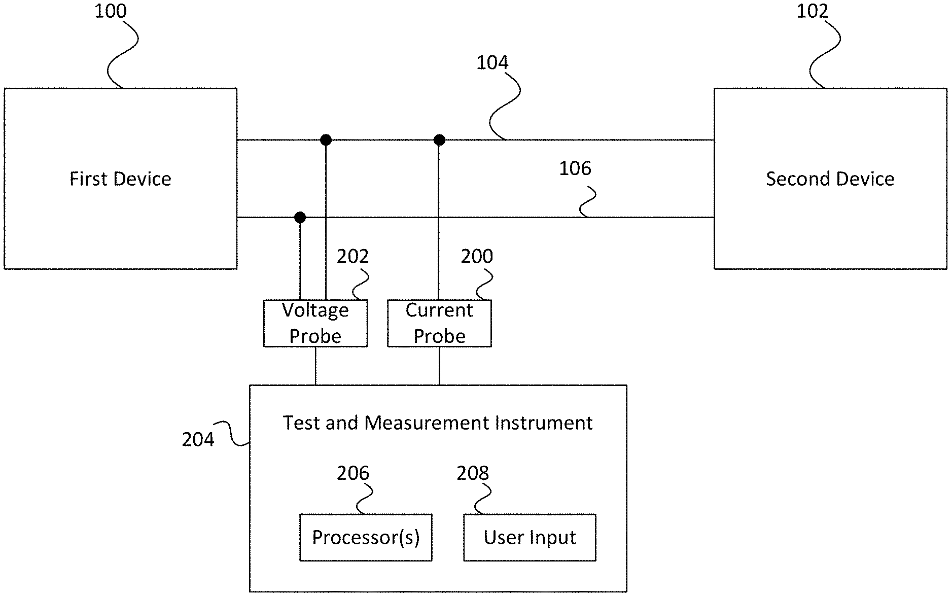
| Assignee: | Tektronix, Inc. Beaverton OR |
||||||||||
| Family ID: | 69055914 | ||||||||||
| Appl. No.: | 16/721677 | ||||||||||
| Filed: | December 19, 2019 |
Related U.S. Patent Documents
| Application Number | Filing Date | Patent Number | ||
|---|---|---|---|---|
| 62807723 | Feb 19, 2019 | |||
| Current U.S. Class: | 1/1 |
| Current CPC Class: | G01R 19/2509 20130101; H04L 43/50 20130101; H01P 3/003 20130101; H04L 43/12 20130101; H04L 5/1423 20130101; H04L 43/0847 20130101 |
| International Class: | G01R 19/25 20060101 G01R019/25; H01P 3/00 20060101 H01P003/00; H04L 5/14 20060101 H04L005/14 |
Foreign Application Data
| Date | Code | Application Number |
|---|---|---|
| Dec 31, 2018 | IN | 201821049938 |
Claims
1. A test and measurement instrument for extracting waveforms from a differential transmission line, comprising: a first input configured to receive a voltage waveform from a voltage probe electrically coupled to the differential transmission line that electrically connects a first device and a second device; a second input configured to receive a current waveform from a current probe electrically coupled to the differential transmission line; and one or more processors configured to receive the voltage waveform and the current waveform and determine a voltage of the first device and a voltage of the second device based on the voltage waveform and the current waveform.
2. The test and measurement instrument of claim 1, wherein the one or more processors are further configured to determine the voltage of the first device and the voltage of the second device based on an impedance of the differential transmission line.
3. The test and measurement instrument of claim 1, wherein the one or more processors are further configured to determine the voltage of the first device using the following equation: V.sub.Tx=(V.sub.TxRx+I.sub.TxRx*Z)/2, where V.sub.Tx is the voltage of the first device, V.sub.TxRx is the voltage waveform of the transmission line, I.sub.TxRx is the current waveform of the differential transmission line, and Z is an impedance of the differential transmission line.
4. The test and measurement instrument of claim 1, wherein the one or more processors are further configured to determine the voltage of the second device using the following equation: V.sub.Rx=(V.sub.TxRx-I.sub.TxRx*Z)/2, where V.sub.Rx is the voltage of the second device, V.sub.TxRx is the voltage waveform of the transmission line, I.sub.TxRx is the current waveform of the differential transmission line, and Z is an impedance of the differential transmission line.
5. The test and measurement instrument of claim 1, wherein the one or more processors are further configured to determine the voltage of the first device using the following equation: V.sub.Tx=(V.sub.TxRx+I.sub.TxRx*Z/2)/2, where V.sub.Tx is the voltage of the first device, V.sub.TxRx is the voltage waveform of the transmission line, I.sub.TxRx is the current waveform of the differential transmission line, and Z is an impedance of the differential transmission line.
6. The test and measurement instrument of claim 1, wherein the one or more processors are further configured to determine the voltage of the second device using the following equation: V.sub.Rx=(V.sub.TxRx-I.sub.TxRx*Z/2)/2, where V.sub.Rx is the voltage of the second device, V.sub.TxRx is the voltage waveform of the transmission line, I.sub.TxRx is the current waveform of the differential transmission line, and Z is an impedance of the differential transmission line.
7. The test and measurement instrument of claim 1, wherein the one or more processors are further configured to compensate a phase of one of the current waveform or the voltage waveform before determining the voltage of the second device.
8. The test and measurement instrument of claim 1, wherein the differential transmission line is a full-duplex serial communication link.
9. A method for extracting a signal from a first device and a second device on a transmission line connecting a first device and a second device, comprising: receiving a voltage waveform including the signal from the first device and the signal from the second device from a voltage probe electrically coupled to the transmission line; receiving a current waveform from a current probe electrically coupled to the transmission line; and separating the signal of the first device and the signal of the second device from the voltage waveform based on the voltage waveform and the current waveform.
10. The method of claim 9, wherein separating the signal of the first device and the signal of the second device from the voltage waveform includes separating the signal of the first device and the signal of the second device based on an impedance of the differential transmission line.
11. The method of claim 9, wherein separating the signal of the first device includes using the following equation: V.sub.Tx=(V.sub.TxRx+I.sub.TxRx*Z)/2, where V.sub.Tx is the signal of the first device, V.sub.TxRx is the voltage waveform, I.sub.TzRx is the current waveform, and Z is an impedance of the transmission line.
12. The method of claim 9, wherein separating the signal of the second device includes using the following equation: V.sub.Rx=(V.sub.TxRx-I.sub.TxRx*Z)/2, where V.sub.Rx is the signal of the first device, V.sub.TxRx is the voltage waveform, I.sub.TxRx is the current waveform, and Z is an impedance of the transmission line.
13. The method of claim 9, wherein separating the signal of the first device includes using the following equation: V.sub.Tx=(V.sub.TxRx+I.sub.TxRx*Z/2)/2, where V.sub.Tx is the signal of the first device, V.sub.TxRx is the voltage waveform, I.sub.TxRx is the current waveform, and Z is an impedance of the transmission line.
14. The method of claim 9, wherein separating the signal of the second device includes using the following equation: V.sub.Rx=(V.sub.TxRx-I.sub.TxRx*Z/2)/2, where V.sub.Rx is the signal of the first device, V.sub.TxRx is the voltage waveform, I.sub.TxRx is the current waveform, and Z is an impedance of the transmission line.
15. The method of claim 9, further comprising compensating a phase of one of the current waveform or the voltage waveform before separating the signal of the second device.
16. The method of claim 9, wherein the transmission line is a full-duplex serial communication link.
17. One or more computer-readable storage media comprising instructions, which, when executed by one or more processors of a test and measurement instrument, cause the test and measurement instrument to: receive a voltage waveform including a signal from a first device and a signal from a second device from a voltage probe electrically coupled to a communication link between the first device and the second device; receive a current waveform from a current probe electrically coupled to the communication link; separate the signal of the first device from the voltage waveform based on the voltage waveform and the current waveform; and separate the signal of the second device from the voltage waveform based on the voltage waveform and the current waveform.
18. The one or more computer-readable storage media of claim 17, wherein separating the signal of the first device and the signal of the second device from the voltage waveform includes separating the signal of the first device and the signal of the second device based on an impedance of the communication link.
19. The one or more computer-readable storage media of claim 17, further comprising instructions configured to compensate a phase of one of the current waveform or the voltage waveform before separating the signal of the second device.
20. The one or more computer-readable storage media of claim 17, wherein the communication link is a full-duplex serial communication link.
Description
PRIORITY
[0001] This disclosure claims priority from Indian Provisional patent application Serial No. 201821049938 filed Dec. 31, 2018 and titled DUPLEX SIGNAL SEPARATION IN AUTOMOTIVE ETHERNET, and claims benefit of U.S. Provisional Application No. 62/807,723 filed Feb. 19, 2019, and titled TX AND RX SIGNAL SEPARATION FOR FULL DUPLEX SERIAL COMMUNICATION SIGNAL.
FIELD OF THE INVENTION
[0002] This disclosure is directed to systems and methods related to test and measurement systems, and in particular, to methods and devices for measuring a full duplex serial communication signal without disrupting the communication link.
BACKGROUND
[0003] Full duplex communication links between two devices are employed in a wide variety of communication systems. Although signals sent across the communication links are analog, the waveform level conveys the digital logic level information. When communicating using a full duplex communication link, such as a 100 Base T1, 1000 Base T1, etc. each device exchanges information with the other device using training patterns which can allow link parameters to be adjusted by the devices to receive information without error.
[0004] In operation, it can be important to test the signal levels on the line, such as to ensure a low bit error rate and that no redundancy is involved because it is important that no information is misinterpreted and lost.
[0005] If only one device is sending information, an oscilloscope can monitor the signals and information may be decoded and physical layer signal integrity can be analyzed. However, in full duplex communication links, both devices are sending information. The waveforms sent by each device are added, and an oscilloscope is not able to make any sense of the information from the acquired signal without utilizing a signal separation device, which can interject noise into the signals.
[0006] Embodiments of the disclosure address these and other deficiencies of the prior art.
BRIEF DESCRIPTION OF THE DRAWINGS
[0007] Aspects, features and advantages of embodiments of the present disclosure will become apparent from the following description of embodiments in reference to the appended drawings in which:
[0008] FIG. 1 is an example of a conventional test and measurement system for measuring a signal from a device connected to another device via a communication link.
[0009] FIG. 2 is an example of a test and measurement system for extracting signals from the devices according to some embodiments of the disclosure.
[0010] FIG. 3 is another example of a test and measurement system for extracting signals from the devices according to some embodiments of the disclosure.
[0011] FIG. 4 is an example operation for extracting signals from the devices without disrupting the communication link according to some embodiments of the disclosure.
[0012] FIG. 5 includes example plots for extracted signals from the communication link between two devices.
[0013] FIG. 6 includes example diagrams derived from signals extracted according to embodiments of the disclosure.
DESCRIPTION
[0014] Embodiments of the disclosure allow for a duplex signal between two devices to be non-invasively separated into simple signals. FIG. 1 illustrates a conventional system for separating the duplex signal between the two devices 100 and 102. A differential transmission line includes two lines 104 and 106 to send and receive signals between the devices 100 and 102.
[0015] In the conventional system, a directional coupler 108 is inserted into the transmission line between the two devices 100 and 102, as well as by interrupting the transmission lines 104 and 106. The directional coupler 108 can be physically large and there are times when there is not enough space provided between the first device 100 and the second device 102 to use the directional coupler 108.
[0016] The directional coupler 108 can output transmitter signals 110 and 112 to a test and measurement instrument 114, and receiver signals 116 and 118 to the test and measurement instrument 114 for further analysis. However, the signals produced by the directional coupler 108 are approximately 12 to 20 decibels attenuated, depending on the directional coupler, which can make it difficult to measure the signals accurately with a good signal to noise radio (SNR). Further, inserting the directional coupler 108 on the transmission line 104 and 106 can introduce some undesirable effects to the communication signals. And if there are any characteristic differences, such as length, parasitic reactance, etc., between the transmission lines 104 and 108 probing points (that is, the location of the directional coupler 108) from the transmission side and from the receiver side, the receiver signal may not be separated accurately even if the transmission signal is separated properly, or vice versa.
[0017] As will be discussed in more detail below, embodiments of the disclosure allow for separating the duplex signal without the use of a directional coupler. Rather, as will be described in detail, voltage and current probes can be used and the test and measurement instrument can separate the signals based on the information received through the probes.
[0018] FIG. 2 illustrates an example test and measurement system according to some embodiments of the disclosure. Similar to FIG. 1, the test and measurement system includes a first device 100 and a second device 102. The first device 100 and the second device 102 communicate on a common differential transmission line for communicating a full duplex differential signal. The common differential transmission line may be, for example, a full duplex serial communication link such as, but not limited to, 100 Base T1, 1000 Base T1, etc. This type of line is often used, for example, in automotive Ethernet, which uses full-duplex signaling over a single twisted pair of wires, which may operate at a multi-level modulation scheme, such as two or more levels.
[0019] The common differential transmission line includes a first line 104 and a second line 106. Each of the voltage and current waveforms on the transmission line appear as superimposed waveforms. That is, a signal is sent concurrent from the first device and the second device. Looking at it from the view point of the first device 100, the output of the first device 100 is a transmission signal and the output from the second device 102 is the receiver signal. For ease of discussion, the output of the first device 100 will be characterized as the transmission signal, or Tx signal, and the output of the second device 102 will be characterized as the receiver signal, or Rx signal. However, as will be understood by one skilled in the art, both the first device 100 and the second device 102 are concurrently sending and receiving signals on the differential signal lines.
[0020] In the system of FIG. 2, a differential voltage probe 202 is connected to differential signal lines 104 and 106. A current probe 200 is connected to one of the differential signal lines. In FIG. 2, the current probe 200 is connected to transmission line 104, but as will be understood by one skilled in the art, the current probe 200 could be connected to the transmission line 106 instead.
[0021] The output of the current probe 200 and the voltage probe 202 are sent to the test and measurement instrument 204. In a conventional oscilloscope, the signals obtained from probing the transmission lines 104 and 106 are displayed as superimposed signals. However, embodiments of the disclosure include a test and measurement instrument 204 that has one or more processors 206 and/or other hardware that can separate the transmission and receiver signals.
[0022] For ease of discussion, the signal from the first device 100 will be referred to as Tx and the signal from the second device 102 will be referred to as Rx. Each of the signals Tx and Rx may have a high level of 1V and a low level of -1V. However, the levels of the Tx and Rx signals is based on the number of modulation levels. The differential transmission lines can have a differential termination impedance, referred to as Z. This value may be set based on the actual differential termination impedance of the differential transmission line used. For examples below, Z will be set to 100 Ohms in this example. However, as will be understood by one skilled in the art, this value can be set by a user in the test and measurement instrument 204 based on the actual differential termination impedance of the differential termination line used.
[0023] When both the Tx and Rx signals are high, then the measured voltage by the voltage probe 202 at that point will be approximately 2V. At that moment, the current of the Tx signal flows from the first device 100 to the second device 102, while the current of the Rx signal flows from the second device 102 to the first device 100. Since the direction of the Tx and Rx currents are the reverse of each other, the superimposed current measured by the current probe 200 is zero Ampere.
[0024] When both the Tx and Rx signals are low, the voltage probe 202 will read a voltage of -2V, meanwhile the current is still 0 Ampere since the currents are still reverse of each other. However, when the Tx signal is high and the Rx signal is low, the superimposed voltage measured by the voltage probe 202 is 0V, and the superimposed current is 20 mA in this example, which is illustrated in equation (1):
(1V/100.OMEGA.)-(-1V/100.OMEGA.)=20 mA (1)
[0025] When the Tx signal is low and the Rx signal is high, the superimposed voltage measured by the voltage probe 202 is again 0V, and the superimposed current is -20 mA. For purposes of discussion, current flowing from the first device 100 to the second device 102 is defined as a positive current.
[0026] The probed voltage waveform by the voltage probe 202 is referred to as superimposed voltage waveform V.sub.TXRx and the current waveform probed by the current probe 200 will be referred to as superimposed current waveform I.sub.TxRx, and the differential termination impedance will be referred to as Z. The Tx signal voltage will be referred to as V.sub.Tx and the current will be referred to as I.sub.Tx. The Rx signal voltage will be referred to as V.sub.RX and the current will be referred to as I.sub.Rx.
[0027] To extract the Tx voltage signal from the superimposed voltage waveform V.sub.TxRx, the Rx voltage waveform V.sub.Rx has to be subtracted from the superimposed voltage waveform V.sub.TxRx. However, the Rx voltage waveform V.sub.Rx cannot be obtained directly by probing because, as mentioned above, the Tx and Rx signals are superimposed on the transmission lines 104 and 106.
[0028] However, a multiplication of the probed current I.sub.TxRx and the impedance Z is equal to V.sub.Tx less V.sub.Rx. Therefore, adding the superimposed current waveform I.sub.TxRx multiplied by Z to the superimposed voltage waveform V.sub.TxRx results in:
V.sub.TxRxI.sub.TxRx*Z=(V.sub.Tx+V.sub.Rx)(V.sub.Tx-V.sub.Rx)=2V.sub.Tx (2)
Then, V.sub.Tx is equal to:
V.sub.Tx=(V.sub.TxRx+I.sub.TxRx*Z)/2 (3)
[0029] For V.sub.Rx, subtracting the superimposed current waveform I.sub.TxRx multiplied by Z from the superimposed voltage waveform V.sub.TxRx, results in:
V.sub.TxRx-I.sub.TxRx*Z=(V.sub.Tx+V.sub.Rx)(V.sub.Tx-V.sub.Rx)=2V.sub.Rx (4)
Then, V.sub.Rx is equal to:
V.sub.Rx=(V.sub.TxRx-I.sub.TxRx*Z)/2 (5)
[0030] Using these equations, in one embodiment of the disclosure, the one or more processors 206 of the test and measurement instrument 204 can receive the superimposed voltage waveform V.sub.TxRx from the voltage probe 202 at a first input and can receive the superimposed current waveform I.sub.TxRx from the current probe 202 at a second input. Using the differential termination impedance Z, which may be set through a user input 208 or stored in memory, the one or more processors 206 can separate the Tx signal voltage waveform V.sub.Tx and the Rx signal voltage waveform V.sub.Rx from the superimposed voltage waveform V.sub.TxRx.
[0031] When there is a difference between the distance along the transmission line from the first device 100 to the probing point and from the second device 102 to the probing point, e.g., the probing point may be closer to the first device 100, and if there is parasitic reactance over the transmission lines 104 and 106 from the second device 102 and the probing point (such as due to connectors and the longer transmission line), there may be a phase difference between the voltage waveform and the current waveform from the second device 102, even if there is no phase difference between the voltage waveform and the current waveform from the first device 100.
[0032] For example, parasitic inductance of connectors can cause current phase delays. As a result of this, the Rx voltage waveform V.sub.Rx determined from equation (5) may not be accurate. In such a situation, the one or more processors 206 can use digital signal processing to correct the phase difference due to parasitic reactance, and the phase-corrected Rx waveform may be used for the above waveform arithmetic processing, which will allow for extracting the Rx signal more accurately.
[0033] That is, using the embodiment described above, the Tx signal may be extracted using the measured superimposed current waveform I.sub.TxRx and superimposed voltage waveform V.sub.TxRx, while the Rx signal is extracted using the measured superimposed voltage waveform V.sub.TxRx and a delay-corrected current waveform I.sub.TxRx.
[0034] In some embodiments, as illustrated in FIG. 3, a current probe 300 may be connected to both transmission lines 104 and 106 to determine the current on both lines 104 and 106. The differential current waveform obtained by current probe 300 can eliminate common-mode current noise. In some embodiments, the current probe 300 may be two current probes, with one probe connected to line 104 and the other current probe connected to the line 106.
[0035] If the current probe 300 is connected to both lines 104 and 106, the measured superimposed current I.sub.TxRx will have double the amplitude. To account for this, equations (3) and (5) above can be modified as follows:
V.sub.Tx=(V.sub.TxRx+I.sub.TxRx*Z/2)/2 (6)
V.sub.Rx=(V.sub.TxRx-I.sub.TxRx*Z/2)/2 (7)
[0036] FIG. 4 illustrates an example operation for separating the superimposed waveform V.sub.TxRx according to some embodiments. Initially, in operation 400, a deskew operation can be performed between the current probes and the voltage probes to allow for phase calibration between current and voltage measurement systems of the test and measurement instrument 204.
[0037] Once the current and voltage probes have been calibrated, then in operation 402, the full duplex communication signal is concurrently probed with current and voltage probes to acquire the superimposed current waveform I.sub.TxRx and the superimposed voltage waveform V.sub.TxRx at the test and measurement instrument 204.
[0038] In some embodiments, an adaptive filter is used to match the voltage probe and the current probe. This can allow for correct signal separation, and the adaptive filter may be adapted based on the model of the currently used voltage probe and current probe.
[0039] The test and measurement instrument 204 then, in operation 404, extracts the Tx waveform based on the superimposed current waveform I.sub.TxRx and the superimposed voltage waveform V.sub.TxRx, as discussed above. For example, the test and measurement instrument 204 may use one of equations (3) or (6) discussed above to determine the Tx waveforms. The test and measurement instrument 204 may do this by utilizing the one or more processors 206 or using other hardware located in the test and measurement instrument 204.
[0040] In operation 406, the test and measurement instrument 204, through the one or more processors 206 and/or other hardware, can then extract the Rx waveforms using one of equations (4) or (7) discussed above.
[0041] The extracted Tx and Rx waveforms may be saved in a memory, displayed to a user on a display, or may be further analyzed, such as for signal integrity and/or decode analysis.
[0042] In some embodiments, an optional operation 408 may be performed before extracting the Rx waveform in operation 406. In operation 408, the test and measurement instrument 204, through either the one or more processors 206 and/or other hardware, may compensate the phase of the superimposed current waveform I.sub.TxRx, as discussed above. That is, the phase of the superimposed current waveform I.sub.TxRx can be compensated based on the parasitic reactance over the transmission line from the second device 102 to the probing point. In alternative embodiments, rather than compensating the superimposed current waveform I.sub.TxRx, the superimposed voltage waveform V.sub.TxRx may instead be compensated based on the parasitic reactance of the transmission line.
[0043] Further, the extraction of the Tx and the Rx waveforms does not need to be performed linearly, as shown in FIG. 4 for ease of discussion. Rather, the Tx and Rx waveforms may be extracted in parallel for faster processing time, or the Rx waveform may be extracted prior to the Tx waveform.
[0044] FIG. 5 illustrates a number of plots with different waveforms. Plot 500 illustrates a superimposed voltage waveform V.sub.TxRx and plot 502 illustrates a superimposed current waveform I.sub.TxRx. Using the embodiments discussed above, plot 504 illustrates an example of an extracted V.sub.Tx waveform from the superimposed voltage waveform of plot 500. And plot 506 illustrates an example of an extracted V.sub.Rx waveform from the superimposed voltage waveform of plot 500. These waveforms in plots 504 and 506 may then be used for further processing, such as generating eye diagrams.
[0045] FIG. 6 illustrates eye diagrams that were generated by the test and measurement instrument 204 using the extracted waveforms illustrated in plots 504 and 506 of FIG. 5. Eye diagram 600 illustrates an eye diagram derived from an extracted Tx voltage signal, while diagram 602 illustrates an eye diagram derived from an extracted Rx voltage signal in which the phase difference due to parasitic reactance was not corrected. As can be seen in the eye diagram 602, the eye diagram 602 is distorted and the eye openings are relatively small because an optimized Rx signal was not extracted.
[0046] However, eye diagram 604 illustrates an extracted Rx voltage signal when the phase of the current waveform has been compensated. In eye diagram 604, the current waveform has a 3 nanosecond correction of the phase difference applied, compared with the uncompensated eye diagram 602. Eye diagram 606 illustrates an extracted Rx voltage signal when the phase of the current waveform has a 2 nanosecond correction of the phase difference applied, compared with the uncompensated eye diagram 602. When comparing eye diagram 604 and eye diagram 606, it is easy to see that the correction of 2 nanoseconds was not enough, as the eye openings of the eye diagram 606 are not as large.
[0047] Embodiments of the disclosure, as discussed above, allow for the signals from each of the devices to be extracted without having to interrupt the communication signal between the devices, which is required by conventional means for measuring the signals. This can result in more accurate results, as well as a simpler set up and operation for a user.
[0048] Aspects of the disclosure may operate on particularly created hardware, firmware, digital signal processors, or on a specially programmed computer including a processor operating according to programmed instructions. The terms controller or processor as used herein are intended to include microprocessors, microcomputers, Application Specific Integrated Circuits (ASICs), and dedicated hardware controllers. One or more aspects of the disclosure may be embodied in computer-usable data and computer-executable instructions, such as in one or more program modules, executed by one or more computers (including monitoring modules), or other devices. Generally, program modules include routines, programs, objects, components, data structures, etc. that perform particular tasks or implement particular abstract data types when executed by a processor in a computer or other device. The computer executable instructions may be stored on a computer readable storage medium such as a hard disk, optical disk, removable storage media, solid state memory, Random Access Memory (RAM), etc. As will be appreciated by one of skill in the art, the functionality of the program modules may be combined or distributed as desired in various aspects. In addition, the functionality may be embodied in whole or in part in firmware or hardware equivalents such as integrated circuits, FPGA, and the like. Particular data structures may be used to more effectively implement one or more aspects of the disclosure, and such data structures are contemplated within the scope of computer executable instructions and computer-usable data described herein.
[0049] The disclosed aspects may be implemented, in some cases, in hardware, firmware, software, or any combination thereof. The disclosed aspects may also be implemented as instructions carried by or stored on one or more or computer-readable storage media, which may be read and executed by one or more processors. Such instructions may be referred to as a computer program product. Computer-readable media, as discussed herein, means any media that can be accessed by a computing device. By way of example, and not limitation, computer-readable media may comprise computer storage media and communication media.
[0050] Computer storage media means any medium that can be used to store computer-readable information. By way of example, and not limitation, computer storage media may include RAM, ROM, Electrically Erasable Programmable Read-Only Memory (EEPROM), flash memory or other memory technology, Compact Disc Read Only Memory (CD-ROM), Digital Video Disc (DVD), or other optical disk storage, magnetic cassettes, magnetic tape, magnetic disk storage or other magnetic storage devices, and any other volatile or nonvolatile, removable or non-removable media implemented in any technology. Computer storage media excludes signals per se and transitory forms of signal transmission.
[0051] Communication media means any media that can be used for the communication of computer-readable information. By way of example, and not limitation, communication media may include coaxial cables, fiber-optic cables, air, or any other media suitable for the communication of electrical, optical, Radio Frequency (RF), infrared, acoustic or other types of signals.
EXAMPLES
[0052] Illustrative examples of the technologies disclosed herein are provided below. An embodiment of the technologies may include any one or more, and any combination of, the examples described below.
[0053] Example 1 a test and measurement instrument for extracting waveforms from a differential transmission line, comprising a first input configured to receive a voltage waveform from a voltage probe electrically coupled to the differential transmission line that electrically connects a first device and a second device; a second input configured to receive a current waveform from a current probe electrically coupled to the differential transmission line; and one or more processors configured to receive the voltage waveform and the current waveform and determine a voltage of the first device and a voltage of the second device based on the voltage waveform and the current waveform.
[0054] Example 2 is the test and measurement instrument of example 1, wherein the one or more processors are further configured to determine the voltage of the first device and the voltage of the second device based on an impedance of the differential transmission line.
[0055] Example 3 is the test and measurement instrument of either one of examples 1 and 2, wherein the one or more processors are further configured to determine the voltage of the first device using the following equation:
V.sub.Tx-(V.sub.TxRx+I.sub.TxRx*Z)/2,
[0056] where V.sub.Tx is the voltage of the first device, V.sub.TxRx is the voltage waveform of the transmission line, I.sub.TxRx is the current waveform of the differential transmission line, and Z is an impedance of the differential transmission line.
[0057] Example 4 is the test and measurement instrument of any one of examples 1-3, wherein the one or more processors are further configured to determine the voltage of the first device using the following equation:
V.sub.Rx=(V.sub.TxRx-I.sub.TxRx*Z)/2,
[0058] where V.sub.Rx is the voltage of the second device, V.sub.TxRx is the voltage waveform of the transmission line, I.sub.TxRx is the current waveform of the differential transmission line, and Z is an impedance of the differential transmission line.
[0059] Example 5 is the test and measurement instrument of any one of examples 1, 2, and 4, wherein the one or more processors are further configured to determine the voltage of the first device using the following equation:
V.sub.Tx=(V.sub.TxRx+I.sub.TxRx*Z/2)/2,
[0060] where V.sub.Tx is the voltage of the first device, V.sub.TxRx is the voltage waveform of the transmission line, I.sub.TxRx is the current waveform of the differential transmission line, and Z is an impedance of the differential transmission line.
[0061] Example 6 is the test and measurement instrument of any one of examples 1, 2, 3, and 5, wherein the one or more processors are further configured to determine the voltage of the first device using the following equation:
V.sub.Rx=(V.sub.TxRx-I.sub.TxRx*Z/2)/2,
[0062] where V.sub.Rx is the voltage of the second device, V.sub.TxRx is the voltage waveform of the transmission line, I.sub.TxRx is the current waveform of the differential transmission line, and Z is an impedance of the differential transmission line.
[0063] Example 7 is the test and measurement instrument of any one of examples 1-6, wherein the one or more processors are further configured to compensate a phase of one of the current waveform or the voltage waveform before determining the voltage of the second device.
[0064] Example 8 is the test and measurement instrument of any one of examples 1-7, wherein the differential transmission line is a full-duplex serial communication line.
[0065] Example 9 is a method for extracting a signal from a first device and a second device on a transmission line connecting a first device and a second device, comprising receiving a voltage waveform including the signal from the first device and the signal from the second device from a voltage probe electrically coupled to the transmission line; receiving a current waveform from a current probe electrically coupled to the transmission line; and separating the signal of the first device and the signal of the second device from the voltage waveform based on the voltage waveform and the current waveform.
[0066] Example 10 is the method of example 9, wherein separating the signal of the first device and the signal of the second device from the voltage waveform includes separating the signal of the first device and the signal of the second device based on an impedance of the differential transmission line.
[0067] Example 11 is the method of either one of examples 9 or 10, wherein separating the signal of the first device includes using the following equation:
V.sub.Tx=(V.sub.TxRx+I.sub.TxRx*Z)/2,
[0068] where V.sub.Tx is the signal of the first device, V.sub.TxRx is the voltage waveform, I.sub.TxRx is the current waveform, and Z is an impedance of the transmission line.
[0069] Example 12 is the method of any one of examples 9-11, wherein separating the signal of the second device includes using the following equation:
V.sub.Rx=(V.sub.TxRx-I.sub.TxRx*Z)/2,
[0070] where V.sub.Rx is the signal of the first device, V.sub.TxRx is the voltage waveform, I.sub.TxRx is the current waveform, and Z is an impedance of the transmission line.
[0071] Example 13 is the method of any one of examples 9, 10, or 12, wherein separating the signal of the first device includes using the following equation:
V.sub.Tx=(V.sub.TxRx+I.sub.TxRx*Z/2)/2,
[0072] where V.sub.Tx is the signal of the first device, V.sub.TxRx is the voltage waveform, I.sub.TxRx is the current waveform, and Z is an impedance of the transmission line.
[0073] Example 14 is the method of any one of examples 9-11 or 13, wherein separating the signal of the second device includes using the following equation:
V.sub.Rx=(V.sub.TxRx-I.sub.TxRx*Z/2)/2,
[0074] where V.sub.Rx is the signal of the first device, V.sub.TxRx is the voltage waveform, I.sub.TxRx is the current waveform, and Z is an impedance of the transmission line.
[0075] Example 15 is the method of any of examples 9-14, further comprising compensating a phase of one of the current waveform or the voltage waveform before separating the signal of the second device.
[0076] Example 16 is the method of any one of examples 9-15, wherein the transmission line is a full-duplex serial communication line.
[0077] Example 17 is one or more computer-readable storage media comprising instructions, which, when executed by one or more processors of a test and measurement instrument, cause the test and measurement instrument to receive a voltage waveform including a signal from a first device and a signal from a second device from a voltage probe electrically coupled to a communication link between the first device and the second device; receive a current waveform from a current probe electrically coupled to the communication link; separate the signal of the first device from the voltage waveform based on the voltage waveform and the current waveform; and separate the signal of the second device from the voltage waveform based on the voltage waveform and the current waveform.
[0078] Example 18 is the one or more computer-readable storage media of example 17, wherein separating the signal of the first device and the signal of the second device from the voltage waveform includes separating the signal of the first device and the signal of the second device based on an impedance of the differential transmission line
[0079] Example 19 is the one or more computer-readable storage media of either one of examples 17 or 18, further comprising instructions configured to compensate a phase of one of the current waveform or the voltage waveform before separating the signal of the second device
[0080] Example 20 is the one or more computer-readable storage media of any one of examples 17-19, wherein the communication link is a full-duplex serial communication link.
[0081] The previously described versions of the disclosed subject matter have many advantages that were either described or would be apparent to a person of ordinary skill. Even so, these advantages or features are not required in all versions of the disclosed apparatus, systems, or methods.
[0082] Additionally, this written description makes reference to particular features. It is to be understood that the disclosure in this specification includes all possible combinations of those particular features. Where a particular feature is disclosed in the context of a particular aspect or example, that feature can also be used, to the extent possible, in the context of other aspects and examples.
[0083] Also, when reference is made in this application to a method having two or more defined steps or operations, the defined steps or operations can be carried out in any order or simultaneously, unless the context excludes those possibilities.
[0084] Although specific examples of the invention have been illustrated and described for purposes of illustration, it will be understood that various modifications may be made without departing from the spirit and scope of the invention. Accordingly, the invention should not be limited except as by the appended claims.
* * * * *
D00000
D00001
D00002
D00003
D00004
D00005
D00006
XML
uspto.report is an independent third-party trademark research tool that is not affiliated, endorsed, or sponsored by the United States Patent and Trademark Office (USPTO) or any other governmental organization. The information provided by uspto.report is based on publicly available data at the time of writing and is intended for informational purposes only.
While we strive to provide accurate and up-to-date information, we do not guarantee the accuracy, completeness, reliability, or suitability of the information displayed on this site. The use of this site is at your own risk. Any reliance you place on such information is therefore strictly at your own risk.
All official trademark data, including owner information, should be verified by visiting the official USPTO website at www.uspto.gov. This site is not intended to replace professional legal advice and should not be used as a substitute for consulting with a legal professional who is knowledgeable about trademark law.