Component Carrier Having a Component Shielding and Method of Manufacturing the Same
Lee; Minwoo
U.S. patent application number 16/726288 was filed with the patent office on 2020-06-25 for component carrier having a component shielding and method of manufacturing the same. The applicant listed for this patent is AT&S (Chongqing) Company Limited. Invention is credited to Minwoo Lee.
| Application Number | 20200205280 16/726288 |
| Document ID | / |
| Family ID | 69005581 |
| Filed Date | 2020-06-25 |


| United States Patent Application | 20200205280 |
| Kind Code | A1 |
| Lee; Minwoo | June 25, 2020 |
Component Carrier Having a Component Shielding and Method of Manufacturing the Same
Abstract
A component carrier and a method of manufacturing the same are disclosed. The component carrier has a stack with at least one electrically conductive layer structure and/or at least one electrically insulating layer structure, and a component embedded in the stack. Sidewalls of the component are directly covered with an electrically conductive layer. The component carrier achieves enhanced thermal dissipation and EMI shielding characteristics and has an improved stiffness.
| Inventors: | Lee; Minwoo; (Chongqing, CN) | ||||||||||
| Applicant: |
|
||||||||||
|---|---|---|---|---|---|---|---|---|---|---|---|
| Family ID: | 69005581 | ||||||||||
| Appl. No.: | 16/726288 | ||||||||||
| Filed: | December 24, 2019 |
| Current U.S. Class: | 1/1 |
| Current CPC Class: | H05K 1/0209 20130101; H01L 2924/3025 20130101; H01L 24/19 20130101; H05K 1/0219 20130101; H01L 2224/32225 20130101; H01L 2224/96 20130101; H01L 2924/3511 20130101; H01L 2224/32245 20130101; H01L 23/552 20130101; H01L 2224/04105 20130101; H01L 23/5389 20130101; H05K 1/0206 20130101; H01L 23/3677 20130101; H05K 3/4644 20130101; H01L 2224/73267 20130101; H01L 2224/92244 20130101 |
| International Class: | H05K 1/02 20060101 H05K001/02; H05K 3/46 20060101 H05K003/46 |
Foreign Application Data
| Date | Code | Application Number |
|---|---|---|
| Dec 25, 2018 | CN | 201811591034.7 |
Claims
1. A component carrier, comprising: a stack comprising at least one electrically conductive layer structure and/or at least one electrically insulating layer structure; and a component embedded in the stack; wherein sidewalls of the component are directly covered with an electrically conductive layer.
2. The component carrier according to claim 1, wherein the electrically conductive layer substantially has a constant thickness.
3. The component carrier according to claim 1, wherein the electrically conductive layer also covers, in particular directly, one or two main surfaces of the component.
4. The component carrier according to claim 1, wherein an electrically insulating structure is at least partly applied onto the electrically conductive layer and an electrically conductive structure is at least partly applied on the electrically insulating structure, and a thermally conductive and electrically insulating structure is arranged between the electrically conductive layer and the electrically conductive structure.
5. The component carrier according to claim 3, wherein a portion of the electrically conductive layer covering the main surface of the component is thermally coupled to an exterior surface of the component carrier by at least one thermal via, in particular an array of thermal vias.
6. The component carrier according to claim 4, wherein a portion of the electrically conductive layer covering the main surface of the component is thermally coupled to an exterior surface of the component carrier by at least one thermal via, in particular an array of thermal vias.
7. The component carrier according to claim 5, wherein an electrically insulating structure is at least partly applied onto the electrically conductive layer and the at least one thermal via, and a thermally conductive and electrically insulating structure is arranged to cover at least partly the at least one thermal via.
8. The component carrier according to claim 6, wherein an electrically insulating structure is at least partly applied onto the electrically conductive layer and the at least one thermal via, and a thermally conductive and electrically insulating structure is arranged to cover at least partly the at least one thermal via.
9. The component carrier according to claim 1, wherein the electrically conductive layer is at least one of a thermal layer and a shielding layer.
10. The component carrier according to claim 3, wherein the electrically conductive layer is at least one of a thermal layer and a shielding layer.
11. The component carrier according to claim 4, wherein the electrically conductive layer is at least one of a thermal layer and a shielding layer.
12. The component carrier according to claim 5, wherein the electrically conductive layer is at least one of a thermal layer and a shielding layer.
13. The component carrier according to claim 1, wherein the component is a naked semiconductor chip.
14. The component carrier according to claim 3, wherein the component is a naked semiconductor chip.
15. The component carrier according to claim 4, wherein the component is a naked semiconductor chip.
16. The component carrier according to claim 1, wherein the component is a semiconductor chip including a surface portion coated by a dielectric.
17. The component carrier according to claim 1, wherein the component includes a plasma treated surface portion.
18. The component carrier according to claim 1, wherein a portion of the stack above the embedded component forms a redistribution structure.
19. The component carrier according to claim 1, wherein the electrically conductive layer consists of at least two metal layers, in particular a sputtered layer and a galvanic layer.
20. The component carrier according to claim 1, comprising at least one of the following features: the component carrier comprises at least one component being surface mounted on and/or embedded in the component carrier, wherein the at least one component is in particular selected from a group consisting of an electronic component, an electrically non-conductive and/or electrically conductive inlay, a heat transfer unit, a light guiding element, an energy harvesting unit, an active electronic component, a passive electronic component, an electronic chip, a storage device, a filter, an integrated circuit, a signal processing component, a power management component, an optoelectronic interface element, a voltage converter, a cryptographic component, a transmitter and/or receiver, an electromechanical transducer, an actuator, a microelectromechanical system, a microprocessor, a capacitor, a resistor, an inductance, an accumulator, a switch, a camera, an antenna, a magnetic element, a further component carrier, and a logic chip; wherein at least one of the electrically conductive layer structures of the component carrier comprises at least one of the group consisting of copper, aluminum, nickel, silver, gold, palladium, and tungsten, any of the mentioned materials being optionally coated with supra-conductive material such as graphene; wherein the electrically insulating layer structure comprises at least one of the group consisting of resin, in particular reinforced or non-reinforced resin, for instance epoxy resin or bismaleimide-triazine resin, FR-4, FR-5, cyanate ester, polyphenylene derivate, glass, prepreg material, polyimide, polyamide, liquid crystal polymer, epoxy-based build-up material, polytetrafluoroethylene, a ceramic, and a metal oxide; wherein the component carrier is shaped as a plate; wherein the component carrier is configured as one of the group consisting of a printed circuit board, a substrate, and an interposer; wherein the component carrier is configured as a laminate-type component carrier.
Description
CROSS-REFERENCE TO RELATED APPLICATION
[0001] This application claims the benefit of the filing date of the Chinese patent application no. 201811591034.7 filed on Dec. 25, 2018, which is incorporated herein by reference in its entirety.
TECHNICAL FIELD
[0002] Embodiments of the invention relate to a component carrier and a method of manufacturing the same.
[0003] Technological Background
[0004] A conventional component carrier comprises a stack having one or more electrically conductive layer structures and one or more electrically insulating layer structures, and a component which is embedded in the stack. The component can be an active or a passive component. For example, U.S. Pat. No. 5,734,555 A describes an electronic package for an integrated circuit (IC). The package has a plurality of first pins extending from a laminated plastic/printed circuit board substrate. The pins are coupled to the integrated circuit and provide a means for mounting the package to an external printed circuit board. The package also has an internal circuit board that is coupled to both the substrate and the IC by a plurality of second pins. Mounted to the circuit board are passive and/or active electrical elements that are connected to the integrated circuit through the second pins. Some of the second pins may extend entirely through the substrate to directly couple the internal circuit board and electrical elements to the external printed circuit board. To improve the thermal impedance of the package, the integrated circuit is mounted to a heat slug which can be attached to a heat sink. The heat sink may also provide a substrate for the internal circuit board.
SUMMARY
[0005] There is a need to provide a component carrier and a method of manufacturing the same, by which the thermal dissipation is enhanced.
[0006] This need may be met by a component carrier and a method of manufacturing the same according to the independent claims.
[0007] According to an exemplary embodiment of the invention, a component carrier is provided. The component carrier comprises a stack comprising at least one electrically conductive layer structure and/or at least one electrically insulating layer structure, and a component embedded in the stack. Sidewalls of the component are directly covered with an electrically conductive layer. In an embodiment, all sidewalls of the component are directly covered with an electrically conductive layer.
[0008] According to another exemplary embodiment of the invention, a method of manufacturing a component carrier includes the following steps: forming a stack comprising at least one electrically conductive layer structure and/or at least one electrically insulating layer structure; embedding a component in the stack; and directly covering sidewalls of the component with an electrically conductive layer.
Overview of Embodiments
[0009] In the context of the present invention, the term "electrically conductive" does not necessarily mean that electricity actually flows in the electrically conductive layer. The term "electrically conductive" rather means that the electrically conductive layer is made of a material which has a suitability to conduct an electric current. For example, the electrically conductive layer can exclusively be a thermal layer which transfers heat without carrying any electric current. The material of the electrically conductive layer can be copper. Alternatively, nickel, aluminum, silver and gold can be used.
[0010] In the context of the present invention, the term "sidewall" means a wall of the component which is substantially perpendicularly orientated to main surfaces of the component. The main surface can include or be a top surface or a bottom surface of the component. The top surface of the component can be that surface of the component, where contacts of the component are arranged. For example, if the component has a cuboid shape, the same has one top surface, one bottom surface being opposed to the top surface, and four sidewalls at four sides of the component, wherein the sidewalls connect the top and bottom surfaces, respectively.
[0011] It is possible but not necessary that the sidewalls are completely covered by the electrically conductive layer. The sidewalls can at least partly be covered by the electrically conductive layer.
[0012] The electrically conductive layer, which can be a copper layer, is placed onto the component, which can be a die, so that the thermal characteristics and moreover a good EMI shielding (electromagnetic interference shielding) can be achieved. If all sidewalls of the component are directly covered with an electrically conductive layer, the thermal dissipation and the EMI shielding effect can be maximized.
[0013] The electrically conductive layer can also achieve a flat component carrier having a good stiffness. Thereby, warping of the component carrier can be avoided.
[0014] According to another exemplary embodiment of the invention, a method of manufacturing a component carrier is provided. The method comprises steps of forming a stack comprising at least one electrically conductive layer structure and/or at least one electrically insulating layer structure, embed-ding a component in the stack, and directly covering sidewalls of the component with an electrically conductive layer. The method achieves the same advantages like the above described component carrier.
[0015] In the following, further exemplary embodiments of the present invention will be explained.
[0016] In an embodiment, the electrically conductive layer substantially has a constant thickness. In the context of the present invention, the term "constant thickness" means that a variation in the thickness of the electrically conductive layer is preferably in a range smaller than 20%, more preferred in a range smaller than 10% and most preferred in a range smaller than 5%.
[0017] In an embodiment, the electrically conductive layer also covers, in particular directly, one or two main surfaces of the component. In the context of the present invention, the term "main surface" can include or be a top surface and a bottom surface of the component. For example, a main surface can be that surface of the component where the contacts of the component are arranged, or a main surface can be that surface of the component which is in parallel to a main surface of the component carrier.
[0018] For example, only one of the top and bottom surfaces of the component can be covered by the electrically conductive layer. Alternatively, both of the top and bottom surfaces of the component can be covered by the electrically conductive layer. By covering at least one main surface of the component, a further improved EMI shielding of the component can be achieved. In particular when both of the top and bottom surfaces of the component are covered by the electrically conductive layer, a kind of shielding cage is provided to surround the component.
[0019] In an embodiment, an electrically insulating structure is at least partly applied onto the electrically conductive layer and an electrically conductive structure is at least partly applied on the electrically insulating structure, and a thermally conductive and electrically insulating structure is arranged between the electrically conductive layer and the electrically conductive structure.
[0020] In an embodiment, a portion of electrically conductive layer covering the main surface of the component is thermally coupled to an exterior surface of the component carrier by at least one thermal via, in particular an array of thermal vias. The thermal vias of the array can optionally be connected by a metal layer which extends in parallel to the exterior surface of the component carrier. By the array of thermal vias and optionally by the metal layer, the thermal dissipation is remarkably enhanced.
[0021] In an embodiment, an electrically insulating structure is at least partly applied onto the electrically conductive layer and the at least one thermal via, and a thermally conductive and electrically insulating structure is arranged to cover at least partly the at least one thermal via.
[0022] In an embodiment, the electrically conductive layer is at least one of a thermal layer and a shielding layer. Since the electrically conductive layer functions as the thermal layer, the same is usually formed of a material in a thickness, which allows sufficient heat transfer. One the one hand, it is not necessary that electricity is actually conducted through the electrically conductive layer. On the other hand, the electrically conductive layer may have a double function to conduct heat and electricity as well. The shielding layer may exhibit an EMI shielding effect which can be measured by a damping of electromagnetic radiation.
[0023] In an embodiment, the component is a naked semiconductor chip. Thereby, the electrically conductive layer can be formed by sputtering, for example. In the context of the present invention, the term "naked semiconductor chip" means that an outer surface of the semiconductor chip consists of or is a semiconductor material, for example silicon or gallium.
[0024] In an embodiment, the component is a semiconductor chip including a surface portion coated by a dielectric. Due to the coated surface portion, the electrically conductive layer can then be formed by forming a seed layer and subsequently plating, i.e. the plating is performed on the seed layer. The seed layer has a low thickness but improves the adhesion of the subsequent plating layer to the component. The plating layer usually has a much larger thickness than the seed layer.
[0025] In an embodiment, the component includes a plasma treated surface portion. Thereby, component surface is activated and its adhesion is enhanced, in particular when the component is a naked semiconductor chip.
[0026] In an embodiment, a portion of the stack above the embedded component forms a redistribution structure so that the component carrier has a function of an adapter. Moreover, an excellent fan-out can be achieved.
[0027] In the context of the present invention, the term "above the embedded component" may refer to a portion outside the component and adjacent a surface of the component, where the contacts of the component are arranged. For example, that surface of the component can be the top surface of the component.
[0028] In an embodiment, the component carrier comprising at least one of the following features: the component carrier comprises at least one component being surface mounted on and/or embedded in the component carrier, wherein the at least one component is in particular selected from a group consisting of an electronic component, an electrically non-conductive and/or electrically conductive inlay, a heat transfer unit, a light guiding element, an energy harvesting unit, an active electronic component, a passive electronic component, an electronic chip, a storage device, a filter, an integrated circuit, a signal processing component, a power management component, an optoelectronic interface element, a voltage converter, a cryptographic component, a transmitter and/or receiver, an electromechanical transducer, an actuator, a microelectromechanical system, a microprocessor, a capacitor, a resistor, an inductance, an accumulator, a switch, a camera, an antenna, a magnetic element, a further component carrier, and a logic chip; wherein at least one of the electrically conductive layer structures of the component carrier comprises at least one of the group consisting of copper, aluminum, nickel, silver, gold, palladium, and tungsten, any of the mentioned materials being optionally coated with supra-conductive material such as graphene; wherein the electrically insulating layer structure comprises at least one of the group consisting of resin, in particular reinforced or non-reinforced resin, for instance epoxy resin or bismaleimide-triazine resin, FR-4, FR-5, cyanate ester, polyphenylene derivate, glass, prepreg material, polyimide, polyamide, liquid crystal polymer, epoxy-based build-up material, polytetrafluoroethylene, a ceramic, and a metal oxide; wherein the component carrier is shaped as a plate; wherein the component carrier is configured as one of the group consisting of a printed circuit board, a substrate, and an interposer; wherein the component carrier is configured as a laminate-type component carrier.
[0029] In an embodiment, the electrically conductive layer consists of at least two metal layers, in particular a sputtered layer and a galvanic layer. The sputtered layer enables an excellent coupling between the galvanic layer and the component.
[0030] In an embodiment of the method, the sidewalls of the component are directly covered with the electrically conductive layer substantially having a constant thickness.
[0031] In an embodiment of the method, also one or two main surfaces of the component are, in particular directly, covered by the electrically conductive layer. The main surfaces can either be the top or the bottom surface of the component.
[0032] In an embodiment of the method, a portion of electrically conductive layer covering the main surface of the component is thermally coupled to an exterior surface of the component carrier by at least one thermal via, in particular an array of thermal vias, so that the thermal dissipation is further enhanced.
[0033] In an embodiment of the method, the electrically conductive layer is formed at least as one of a thermal layer and a shielding layer so that a good heat dissipation and/or a good EMI shielding characteristic can be achieved.
[0034] In an embodiment of the method, the electrically conductive layer is formed by sputtering. This is particularly useful when the component is a naked semiconductor chip, i.e. the outer surfaces thereof are made of a semiconductor material such as silicon or gallium, etc.
[0035] In an embodiment of the method, the electrically conductive layer is formed by forming a seed layer, in particular by sputtering, and subsequently plating, in particular by galvanic plating. This is particularly useful when the component is a semiconductor chip including a surface portion coated by a dielectric.
[0036] In an embodiment of the method, a surface portion of the component is treated by plasma. Thereby, the components surface is activated to enhance the adhesion. This is particularly useful when the component is a naked semiconductor chip, i.e. the outer surfaces thereof are made of a semiconductor material such as silicon or gallium, etc.
[0037] In the context of the present application, the term "component carrier" may particularly denote any support structure which is capable of accommodating one or more components thereon and/or therein for providing mechanical support and/or electrical connectivity. In other words, a component carrier may be configured as a mechanical and/or electronic carrier for components. In particular, a component carrier may be one of a printed circuit board, an organic interposer, and an IC (integrated circuit) substrate. A component carrier may also be a hybrid board combining different ones of the above-mentioned types of component carriers.
[0038] In an embodiment, the component carrier comprises a stack of at least one electrically insulating layer structure and at least one electrically conductive layer structure. For example, the component carrier may be a laminate of the mentioned electrically insulating layer structure(s) and electrically conductive layer structure(s), in particular formed by applying mechanical pressure and/or thermal energy. The mentioned stack may provide a plate-shaped component carrier capable of providing a large mounting surface for further components and being nevertheless very thin and compact. The term "layer structure" may particularly denote a continuous layer, a patterned layer or a plurality of non-consecutive islands within a common plane.
[0039] In an embodiment, the component carrier is shaped as a plate. This contributes to the compact design, wherein the component carrier nevertheless provides a large basis for mounting components thereon. Furthermore, in particular a naked die as example for an embedded electronic component, can be conveniently embedded, thanks to its small thickness, into a thin plate such as a printed circuit board.
[0040] In an embodiment, the component carrier is configured as one of the group consisting of a printed circuit board, a substrate (in particular an IC substrate), and an interposer.
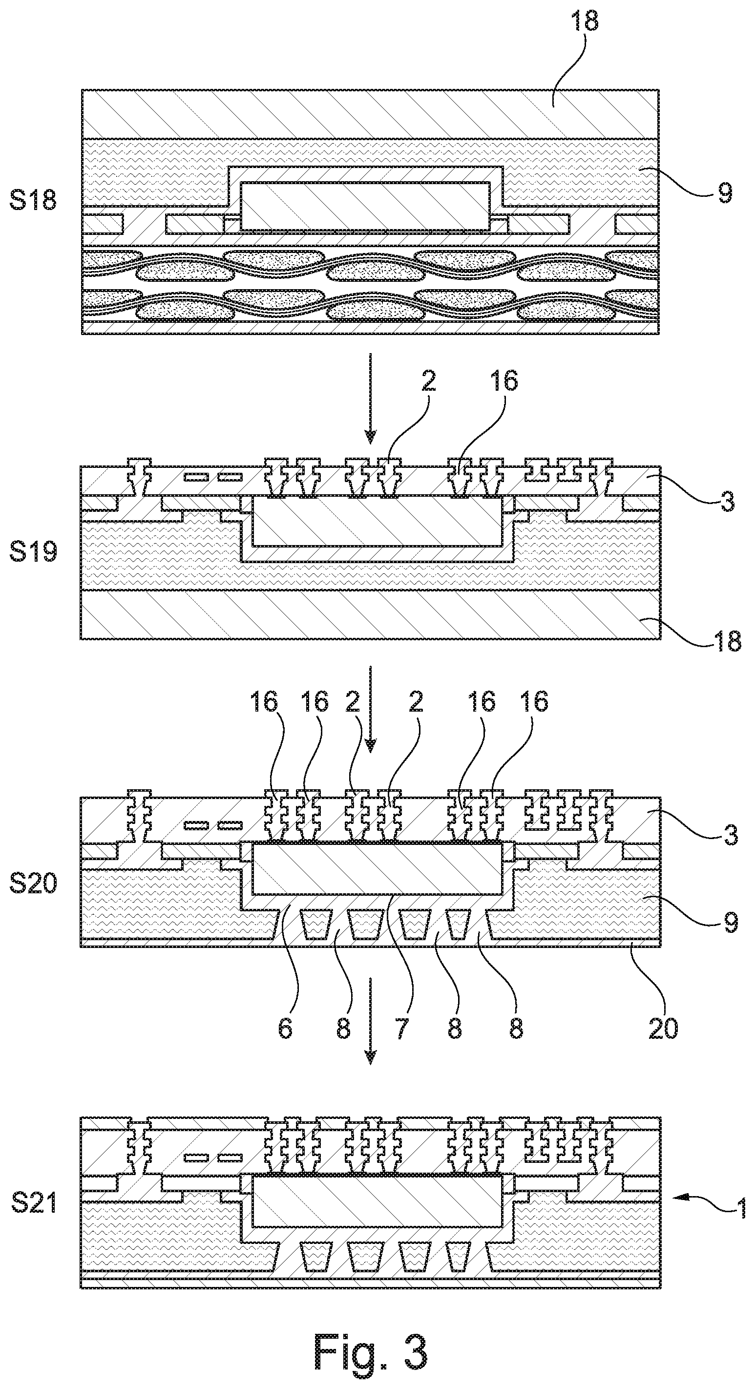
[0041] In the context of the present application, the term "printed circuit board" (PCB) may particularly denote a plate-shaped component carrier which is formed by laminating several electrically conductive layer structures with several electrically insulating layer structures, for instance by applying pressure and/or by the supply of thermal energy. As preferred materials for PCB technology, the electrically conductive layer structures are made of copper, whereas the electrically insulating layer structures may comprise resin and/or glass fibers, so-called prepreg or FR4 material. The various electrically conductive layer structures may be connected to one another in a desired way by forming through-holes through the laminate, for instance by laser drilling or mechanical drilling, and by filling them with electrically conductive material (in particular copper), thereby forming vias as through-hole connections. Apart from one or more components which may be embedded in a printed circuit board, a printed circuit board is usually configured for accommodating one or more components on one or both opposing surfaces of the plate-shaped printed circuit board. They may be connected to the respective main surface by soldering. A dielectric part of a PCB may be composed of resin with reinforcing fibers (such as glass fibers).
[0042] In the context of the present application, the term "substrate" may particularly denote a small component carrier having substantially the same size as a component (in particular an electronic component) to be mounted thereon. More specifically, a substrate can be understood as a carrier for electrical connections or electrical networks as well as component carrier comparable to a printed circuit board (PCB), however with a considerably higher density of laterally and/or vertically arranged connections. Lateral connections are for example conductive paths, whereas vertical connections may be for example drill holes. These lateral and/or vertical connections are arranged within the substrate and can be used to provide electrical and/or mechanical connections of housed components or unhoused components (such as bare dies), particularly of IC chips, with a printed circuit board or intermediate printed circuit board. Thus, the term "substrate" also includes "IC substrates". A dielectric part of a substrate may be composed of resin with reinforcing particles (such as reinforcing spheres, in particular glass spheres).
[0043] The substrate or interposer may comprise or consist of at least a layer of glass, silicon (Si) or a photo-imageable or dry-etchable organic material like epoxy-based build-up material (such as epoxy-based build-up film) or polymer compounds like polyimide, polybenzoxazole, or benzocyclobutene.
[0044] In an embodiment, the at least one electrically insulating layer structure comprises at least one of the group consisting of resin (such as rein-forced or non-reinforced resins, for instance epoxy resin or bismaleimide-triazine resin), cyanate ester, polyphenylene derivate, glass (in particular glass fibers, multi-layer glass, glass-like materials), prepreg material (such as FR-4 or FR-5), polyimide, polyamide, liquid crystal polymer (LCP), epoxy-based build-up film, polytetrafluoroethylene (Teflon.RTM.), a ceramic, and a metal oxide. Teflon is a registered mark of The Chemours Company FC, LLC of Wilmington, Delware, U.S.A. Reinforcing materials such as webs, fibers or spheres, for example made of glass (multilayer glass) may be used as well. Although prepreg particularly FR4 are usually preferred for rigid PCBs, other materials in particular epoxy-based build-up film for substrates may be used as well. For high frequency applications, high-frequency materials such as polytetrafluoroethylene, liquid crystal polymer and/or cyanate ester resins, low temperature cofired ceramics (LTCC) or other low, very low or ultra-low DK materials may be implemented in the component carrier as electrically insulating layer structure.
[0045] In an embodiment, the at least one electrically conductive layer structure comprises at least one of the group consisting of copper, aluminum, nickel, silver, gold, palladium, and tungsten. Although copper is usually preferred, other materials or coated versions thereof are possible as well, in particular coated with supra-conductive material such as graphene.
[0046] The at least one component can be selected from a group consisting of an electrically non-conductive inlay, an electrically conductive inlay (such as a metal inlay, preferably comprising copper or aluminum), a heat transfer unit (for example a heat pipe), a light guiding element (for example an optical waveguide or a light conductor connection), an electronic component, or combinations thereof. For example, the component can be an active electronic component, a passive electronic component, an electronic chip, a storage device (for instance a DRAM or another data memory), a filter, an integrated circuit, a signal processing component, a power management component, an optoelectronic interface element, a light emitting diode, a photocoupler, a voltage converter (for example a DC/DC converter or an AC/DC converter), a cryptographic component, a transmitter and/or receiver, an electromechanical transducer, a sensor, an actuator, a microelectromechanical system (MEMS), a microprocessor, a capacitor, a resistor, an inductance, a battery, a switch, a camera, an antenna, a logic chip, and an energy harvesting unit. However, other components may be embedded in the component carrier. For example, a magnetic element can be used as a component. Such a magnetic element may be a permanent magnetic element (such as a ferromagnetic element, an antiferromagnetic element or a ferromagnetic element, for instance a ferrite core) or may be a paramagnetic element. However, the component may also be a substrate, an interposer or a further component carrier, for example in a board-in-board configuration. The component may be surface mounted on the component carrier and/or may be embedded in an interior thereof. Moreover, also other components, in particular those which generate and emit electromagnetic radiation and/or are sensitive with regard to electromagnetic radiation propagating from an environment, may be used as component.
[0047] In an embodiment, the component carrier is a laminate-type component carrier. In such an embodiment, the component carrier is a compound of multiple layer structures which are stacked and connected together by applying a pressing force and/or heat.
[0048] According to an exemplary embodiment, a nano-coated structure may be used for component carrier technology, in particular as a dry-adhesive structure. An adhesive layer implementing such a surface configuration may also be denoted as gecko film. The adhesive effect of such a surface may be based on van der Waals forces. Descriptively speaking, a plurality of low dimensioned suction cups may be formed by such a concept. According to an exemplary embodiment of the invention, a reliable substrate and/or structured material is provided for embedding and/or surface mounting applications having specific adhesion properties due to a corresponding configuration of nano- and/or microstructures on this surface. Exemplary embodiments have the advantage that the mentioned adjustability of the surface adhesion properties may be obtained with low material consumption, low production costs, small contamination risk, and high process reliability.
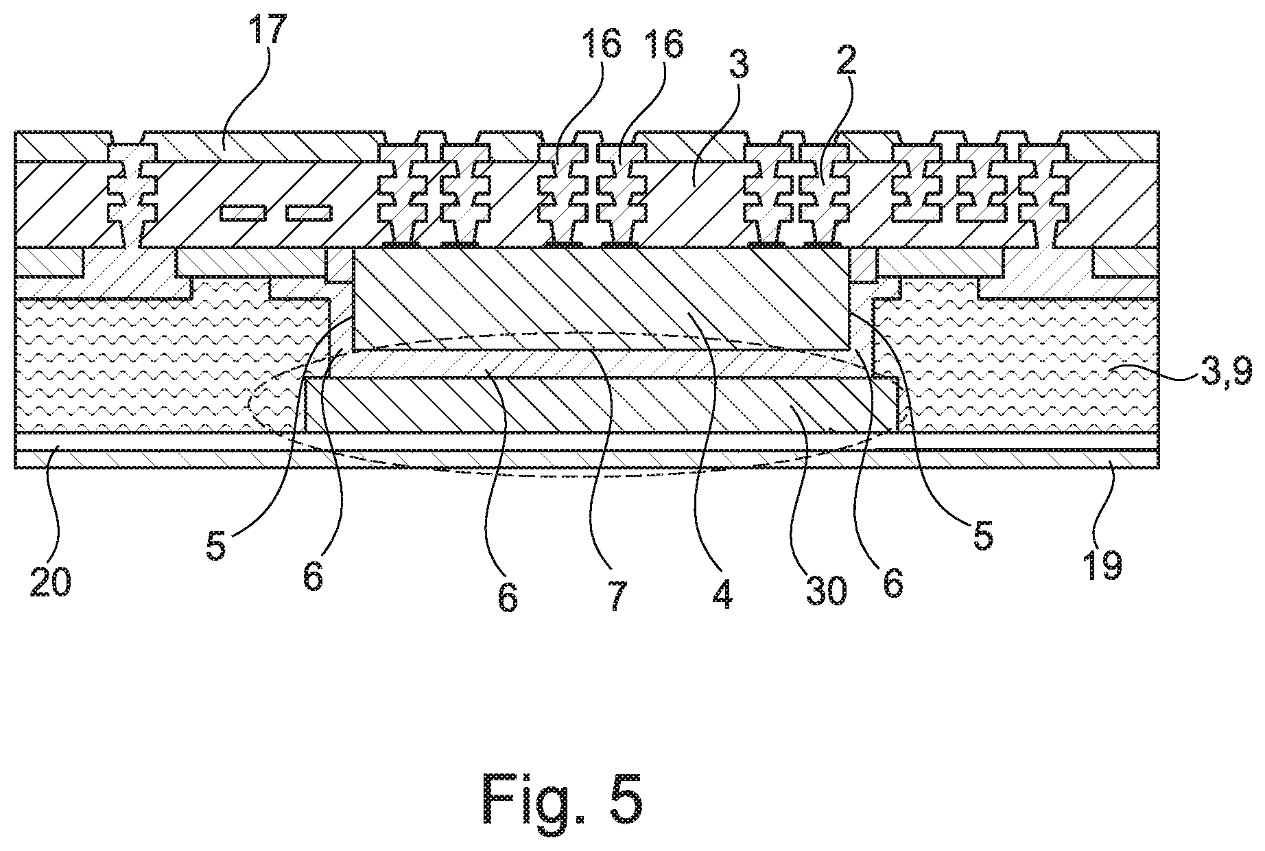
[0049] In an embodiment, the mentioned materials may be used as support for component placement in embedding technologies. Compared to a traditional adhesive tape system that is depending on temperature and time, an exemplary embodiment uses the surface of a support (which may be rigid or flexible) or a PCB elements (such as cores, prepregs, copper foils, etc.), that exhibits, thanks to the nano- and/or microstructures, van der Waals attraction forces, a gecko effect, a high grip, and that is dry and thus can be cleaned and reused. A sheet with nano- and/or microstructures can also be included in the final product. When used for an embedding concept, components may be placed on the dry surface and can be held in position by weak bonds (like van der Waals forces, gecko effect, high grip values) prior to the component lamination.
[0050] Such an architecture allows to obtain a dry interaction between the component and the holding substrate. No additional liquid adhesive is required. This has the advantages of a dry interaction, and a reduction of risk of contamination from the substrate.
[0051] The aspects defined above and further aspects of the invention are apparent from the examples of embodiment to be described hereinafter and are explained with reference to these examples of embodiment.
BRIEF DESCRIPTION OF THE DRAWINGS
[0052] FIG. 1 illustrates a cross-sectional view of a component carrier according to an exemplary embodiment of the invention.
[0053] FIG. 2 illustrates a method of manufacturing a component carrier according to an exemplary embodiment of the invention.
[0054] FIG. 3 illustrates a modification of the method of manufacturing a component carrier of FIG. 2 according to another exemplary embodiment of the invention.
[0055] FIG. 4 illustrates a cross-sectional view of a component carrier according to an exemplary embodiment of the invention.
[0056] FIG. 5 illustrates a cross-sectional view of a component carrier according to an exemplary embodiment of the invention.
[0057] FIG. 6 illustrates a cross-sectional view of a component carrier according to an exemplary embodiment of the invention.
[0058] FIG. 7 illustrates a cross-sectional view of a component carrier according to an exemplary embodiment of the invention.
[0059] FIG. 8 illustrates a cross-sectional view of a component carrier according to an exemplary embodiment of the invention.
DETAILED DESCRIPTION OF ILLUSTRATED EMBODIMENTS
[0060] The illustrations in the drawings are schematically presented. In different drawings, similar or identical elements are provided with the same reference signs.
[0061] FIG. 1 illustrates a cross-sectional view of a component carrier 1 according to an exemplary embodiment of the invention. The component carrier 1 is shaped as a plate. The component carrier 1 can be configured as one of the group consisting of a printed circuit board, a substrate, and an interposer. The component carrier 1 can be configured as a laminate-type component carrier.
[0062] The component carrier 1 comprises a stack comprising a plurality of electrically conductive layer structures 2 and a plurality of electrically insulating layer structures 3.
[0063] The electrically conductive layer structures 2 of the component carrier 1 can comprise at least one of the group consisting of copper, aluminum, nickel, silver, gold, palladium, and tungsten, any of the mentioned materials being optionally coated with supra-conductive material such as graphene.
[0064] The electrically conductive layer structures 2 of the component carrier 1 include electrical vias 16 which are connected to contacts of the component 4.
[0065] The electrically insulating layer structures 3 comprise at least one of the group consisting of resin, in particular reinforced or non-reinforced resin, for instance epoxy resin or bismaleimide-triazine resin, FR-4, FR-5, cyanate ester, polyphenylene derivate, glass, prepreg material, polyimide, polyamide, liquid crystal polymer, epoxy-based build-up film, polytetrafluoroethylene, a ceramic, and a metal oxide.
[0066] A component 4 is embedded in the stack. The component 4 is in particular selected from a group consisting of an electronic component, an electrically non-conductive and/or electrically conductive inlay, a heat transfer unit, a light guiding element, an energy harvesting unit, an active electronic component, a passive electronic component, an electronic chip, a storage device, a filter, an integrated circuit, a signal processing component, a power management component, an optoelectronic interface element, a voltage converter, a cryptographic component, a transmitter and/or receiver, an electromechanical transducer, an actuator, a microelectromechanical system, a microprocessor, a capacitor, a resistor, an inductance, an accumulator, a switch, a camera, an antenna, a magnetic element, a further component carrier, and a logic chip.
[0067] All four sidewalls 5 of the component 4 are at least partly and directly covered with an electrically conductive layer 6. The electrically conductive layer 6 forms a kind of electromagnetic cage surrounding the component 4.
[0068] In the context of the present invention, the term "electrically conductive" does not necessarily mean that electricity actually flows in that layer 6. The term "electrically conductive" rather means that the layer 6 is made of a material which has a suitability to conduct an electric current. For example, the electrically conductive layer 6 can exclusively be a thermal layer 6 which transfers heat without carrying any electric current. The material of the electrically conductive layer 6 can be copper. Alternatively, nickel, aluminum, silver and gold can be used for the electrically conductive layer 6.
[0069] In the context of the present invention, the term "sidewall" means a wall of the component 4 which is substantially perpendicularly orientated to main surfaces of the component. The main surface can include or be the top surface or the bottom surface 7 of the component 4. The top surface of the component 4 can be that surface of the component, where contacts of the component 4 are arranged. Alternatively, the main surface can be that surface of the component 4 which is parallel to a main surface of the component carrier 1. For example, if the component 4 substantially has a cuboid shape, the same has one top surface, one bottom surface 7 being opposed to the top surface, and four sidewalls 5 at four sides of the component 4, wherein the sidewalls 5 connect the top and bottom surfaces, respectively. The number of the sidewalls 5 is not limited to four, in particular in case of a hexagonal or octagonal-shaped main surfaces of the component 4.
[0070] Although all sidewalls 5 of the component 4 are directly covered with an electrically conductive layer 6 in the embodiment of FIG. 1, it is conceivable that only some of the sidewalls 5 are directly covered with an electrically conductive layer 6.
[0071] The electrically conductive layer 6 substantially has a constant thickness. In the context of the present invention, the term "constant thickness" means that a variation in the thickness of the electrically conductive layer 6 is preferably in a range smaller than 20%, more preferred in a range smaller than 10% and most preferred in a range smaller than 5%.
[0072] The electrically conductive layer 6 has a relatively large thickness which ensures that the relative flat component carrier 1 has a good stiffness. Thereby, warping of the component carrier 1 can be minimized.
[0073] The electrically conductive layer 6 also covers one main surface 7 of the component 4. In the context of the present invention, the term "main surface" can include a top surface and a bottom surface of the component 4. In an embodiment, only one of the top and bottom surfaces of the component 4 is covered by the electrically conductive layer 6. For example, in FIG. 1 only the bottom surface 7 of the component 4 is covered by the electrically conductive layer 6. In another embodiment, both of the top and bottom surfaces of the component 4 can be covered by the electrically conductive layer 6. By covering at least one main surface 7 of the component 4, a further improved EMI shielding (electromagnetic interference shielding) of the component 4 can be achieved. If both of the top and bottom surfaces of the component 4 are covered by the electrically conductive layer 6, a kind of electromagnetic cage is provided around the component 4. Furthermore, the heat dissipation and the stiffness of the component carrier 1 are further improved.
[0074] A portion of electrically conductive layer 6 covering the main surface 7 of the component 4 is thermally coupled to an exterior surface of the component carrier 1 by an array of thermal vias 8. At the same time, the electrically conductive layer 6 is a thermal layer to further improve the thermal dissipation. Since the electrically conductive layer 6 functions as the thermal layer, the same is usually formed of a material in a thickness, which allows sufficient heat transfer. One the one hand, it is not necessary that electricity is actually conducted through the electrically conductive layer 6. One the other hand, the electrically conductive layer 6 may have a double function to conduct heat and electricity as well.
[0075] In an embodiment, the component 4 is a naked semiconductor chip. Thereby, the electrically conductive layer 6 can particularly be formed by sputtering. In the context of the present invention, the term "naked semiconductor chip" means that an outer surface of the semiconductor chip consists of or is a semiconductor material, for example silicon or gallium.
[0076] In another embodiment, the component 4 is a semiconductor chip including a surface portion coated by a dielectric. In this case, the electrically conductive layer 6 can be formed by forming a seed layer and subsequently plating. The seed layer has a lower thickness but improves the adhesion of the subsequent plating layer to the component 4. The plating layer usually has a much larger thickness than the seed layer.
[0077] To activate the surface of the component 4, at least a portion of the same can be treated by plasma.
[0078] Although not shown in FIG. 1, a portion of the stack above the embedded component 4 can form a redistribution structure. For example, a pitch between contacts of the component 4 can be larger or smaller than a pitch of external contacts of the component carrier 1. In the context of the present invention, the term "above the embedded component 4" may refer to a portion outside the component 4 and adjacent a surface of the component 4, where the contacts of the component are arranged. For example, that surface of the component 4 can be the top surface of the component 4.
[0079] A solder resist 17 and a surface finish 19 are applied on the stack. The solder resist 17 is applied to that surface of the stack, where the contacts of the component carrier 1 are exposed, and the surface finish 19 is applied to the opposed surface of the stack.
[0080] FIG. 2 illustrates a method of manufacturing a component carrier 1 according to an exemplary embodiment of the invention.
[0081] In a step S1, a temporary carrier 11 is provided. The temporary carrier 11 can comprise a DCF (Detachable Copper Foil) core or a glass carrier. The temporary carrier 11 is laminated at both sides by a detachable copper foil 12.
[0082] In a step S2, a patterning material 13 is applied on one or on both copper foils 12. The patterning material 13 can be a PSR (photosensitive resist) or a PID (photo-imageable dielectric), etc.
[0083] In a step S3, patterning material 13 is patterned. In an embodiment, the patterning can comprise illumination or exposing with electromagnetic radiation through a mask, followed by developing the patterning material 13, followed in turn by a selective removal of either the illuminated portion or the non-illuminated portion of the patterning material 13. The removal can be achieved by an etching chemistry. In step S3, a cavity 14 is formed which is configured to accommodate the component 4.
[0084] In a step S4, an adhesive 15 is applied in the cavity 14. The adhesive 15 can be an electrically non-conductive adhesive. The adhesive 15 can be applied by printing. The adhesive 15 can be applied by other application methods. For example, the adhesive 15 can be printed or sprayed as a film, or the adhesive 15 can be placed into cavity 14 as a pad or a tape. Also, instead of applying the adhesive 15 into the cavity 14, the adhesive 15 can be applied to one surface of the component 4 before the component 4 having the adhesive 15 applied thereon is placed into the cavity 14.
[0085] In a step S5, the component 4 is placed into the cavity 14 and adhered by the adhesive 15. The adhesive 15 can be a thermosetting adhesive which is to be cured.
[0086] In a step S6, the sidewalls 5 and also a bottom surface 7 of the component 4 are directly covered with an electrically conductive layer 6 substantially having a constant thickness. In an embodiment, the electrically conductive layer 6 is formed by sputtering, in particular when the component 4 is a naked semiconductor chip. In another embodiment, the electrically conductive layer 6 is formed by forming a seed layer and subsequently by plating, i.e. the plating is performed on the seed layer which has been formed before. This two-step procedure is applicable when the component 4 is a semiconductor chip including a surface portion coated by a dielectric. The seed layer can be formed by electroless plating or sputtering. The subsequent plating can be made by galvanic plating for example. A thickness of that part of the electrically conductive layer 6, which is made by plating, is usually larger than a thickness of the seed layer of the electrically conductive layer 6. The material of the electrically conductive layer 6 can be copper.
[0087] Before applying the electrically conductive layer 6, a surface portion of the component 4 can be treated by plasma. For example, if the component 4 is a naked semiconductor chip, the outer semiconductor chip surface is activated by the plasma treatment.
[0088] In a step S7, the electrically conductive layer 6 is oxidized so that the surface roughness thereof and/or the electric resistance thereof is enlarged. After that, a filling material 9 is applied onto the electrically conductive layer 6. Thereby, the component carrier 1 is flattened. The filling material 9 can be a dielectric material, a prepreg material, an insulating material such as a build-up-material, in particular build-up-film, or a mold film, etc.
[0089] In FIG. 2, the steps S1 to S7 are performed on only one side of the temporary carrier 11. It is to be noted that the steps S1 to S7 can also be performed on the opposed side of the temporary carrier 11.
[0090] In a step S8, the temporary carrier 11 is detached or delaminated. The detachable copper foils 12 can remain on the stack. Thereafter, a patterning and plating process is performed in which several layers of electrically conductive layer structures 2 and electrically insulating layer structures 3 are build-up on one or both sides of the stack. In particular, on that side of the stack where the contacts of the component 4 are arranged, electrically conductive vias 16 are formed which connect the contacts of the component 4 to the external contacts of the component carrier 1. For example, a portion of the stack above the embedded component 4, i.e. a portion of the electrically conductive layer structures 2 and electrically insulating layer structures 3, can form a redistribution structure, where a pitch between contacts of the component 4 is larger or smaller than a pitch of external contacts of the component carrier 1.
[0091] On the opposed side of the stack, where the contacts of the component 4 are not arranged, the filling material 9 is patterned and plated so that a portion of the electrically conductive layer 6 covering the main surface 7 of the component 4 is thermally coupled to an exterior surface of the component carrier 1 by an array of thermal vias 8. In particular, a copper layer 20, which extends in parallel to the exterior surface of the component carrier 1, connects the array of vias 8.
[0092] In a step S9, a solder resist 17 and a surface finish 19 is applied on the stack. For example, the solder resist 17 can be applied to that surface of the stack, where the contacts of the component carrier 1 are exposed, and the surface finish 19 can be applied to the opposed surface of the stack, for example on the copper layer 20.
[0093] Eventually, the method includes steps of forming a stack comprising at least one electrically conductive layer structure 2 and/or at least one electrically insulating layer structure 3, embedding a component 4 in the stack and directly covering sidewalls 5 of the component 4 with an electrically conductive layer 6.
[0094] FIG. 3 illustrates a modification of the method of manufacturing a component carrier 1 of FIG. 2 according to another exemplary embodiment of the invention. The embodiment of FIG. 3 replaces the steps S8 and S9 of FIG. 2 with modified steps S18 to S21.
[0095] In the step S18, which follows step S7 in FIG. 2, a second temporary carrier 18 is applied on the filling material 9. The second temporary carrier 18 is applied before curing the filling material 9, which can be a dielectric material, a prepreg material, an insulating material such as a build-up-material, in particular a build-up-film, or a mold film. The second temporary carrier 18 improves the stiffness of the temporary component carrier 1 which can be readily aligned during the subsequent manufacturing process and exhibits less warpage.
[0096] In the step S19, the (first) temporary carrier 11 is detached or delaminated, and a first patterning and plating process is performed in which several layers of electrically conductive layer structures 2 and electrically insulating layer structures 3 are build-up on that side of the stack where the contacts of the component 4 are arranged. In particular, electrically conductive vias 16 are formed which are connected to the contacts of the component 4.
[0097] In a step S20, the second temporary carrier 18 is detached or delaminated, and a second patterning and plating process is performed, in which several electrically conductive layer structures 2 and electrically insulating layer structures 3 are build-up on that side of the stack where the contacts of the component 4 are arranged. In particular, the electrically conductive vias 16 are further built-up. It is to be noted that the second patterning and plating process can be omitted.
[0098] Furthermore, on the opposed side of the stack where the contacts of the component 4 are not arranged, a third patterning and plating process is performed in which the filling material 9 is patterned and plated so that a portion of the electrically conductive layer 6 covering the main surface 7 of the component 4 is thermally coupled to an exterior surface of the component carrier 1 by an array of thermal vias 8. In particular, a copper layer 20, which extends in parallel to the exterior surface of the component carrier 1, is plated to connect the array of vias 8.
[0099] In a step S21, a solder resist 17 and a surface finish 19 is applied on the stack. For example, the solder resist 17 can be applied to that surface of the stack, where the contacts of the component carrier 1 are exposed, and the surface finish 19 can be applied to the opposed surface of the stack, for example on the copper layer 20 which extends in parallel to the exterior surface of the component carrier 1.
[0100] FIG. 4 illustrates a cross-sectional view of a component carrier 1 according to an exemplary embodiment of the invention. The component carrier 1 of FIG. 4 is substantially similar to the component carrier 1 of FIG. 1 except for the following differences.
[0101] While the component carrier 1 of FIG. 1 comprises the thermal vias 8 for a heat dissipation from the component 4, the component carrier 1 of FIG. 4 does not need this kind of heat dissipation so that the thermal vias 8 are omitted in the component carrier 1 of FIG. 4. Consequently, also the holes are omitted which define the thermal vias 8. Instead, the filling material 9, which is one of the plurality of electrically insulating layer structures 3, also covers the electrically conductive layer 6 at the side of the bottom surface 7 of the component 4. Furthermore, the copper layer 20 can have the shape of a planar layer and is thermally connected and/or electrically not connected to the electrically conductive layer 6.
[0102] FIG. 5 illustrates a cross-sectional view of a component carrier 1 according to an exemplary embodiment of the invention. The component carrier 1 of FIG. 5 is substantially similar to the component carrier 1 of FIG. 4 except for the following differences.
[0103] Between the copper layer 20 and the electrically conductive layer 6 at the side of the bottom surface 7 of the component 4, a thermally conductive structure 30 is arranged. The thermally conductive structure 30 can have a shape of a block as shown in FIG. 5 or of a planar layer (not shown). The thermally conductive structure 30 can be an inlay. The thermally conductive structure 30 can be made of a metal such as copper or aluminum, or of a thermally conductive but electrically insulating material such as ceramics or a dielectric.
[0104] FIG. 6 illustrates a cross-sectional view of a component carrier 1 according to an exemplary embodiment of the invention. The component carrier 1 of FIG. 6 is substantially similar to the component carrier 1 of FIG. 1 except for the following differences.
[0105] The copper layer 20 is electrically insulated from the electrically conductive layer 6 at the side of the bottom surface 7 of the component 4 in that the copper layer 20 is arranged in a manner that a first portion 31 of the copper layer 20 is formed which is electrically and thermally connected to the array of thermal vias 8, and a second portion 32 and a third portion 33 of the copper layer 20 are formed, which are electrically not connected to the first portion 31. The gaps 32, 33 therebetween are filled by the filling material 9 such as a dielectric material, a prepreg material, an insulating material such as a build-up-material, in particular build-up-film, or a mold film, etc., or by another insulating material which is different from the filling material 9. The gaps 32, 33 can be formed by photolithography and etching methods, or by drilling of the copper layer 20.
[0106] FIG. 7 illustrates a cross-sectional view of a component carrier 1 according to an exemplary embodiment of the invention. The component carrier 1 of FIG. 7 is substantially similar to the component carrier 1 of FIG. 1 except for the following differences.
[0107] The copper layer 20 is patterned, for example by photolithography and etching methods, or by drilling. Thereby, a first portion 31 of the copper layer 20 is formed which is electrically and thermally connected to the array of thermal vias 8, and a second portion 32 and a third portion 33 of the copper layer 20 are formed, which are electrically not connected to the first portion 31. The gaps therebetween are filled by an electrically insulating material 36 such as a dielectric material, a prepreg material, an insulating material such as a build-up-material, in particular build-up-film, or a mold film, etc. In addition, a thermally conductive structure 30 is arranged on first portion 31. The thermally conductive structure 30 can have a shape of a block as shown in FIG. 7 or of a planar layer (not shown). The thermally conductive structure 30 can be an inlay. The thermally conductive structure 30 can be made of a metal such as copper or aluminum, or of a thermally conductive but electrically insulating material such as ceramics or a dielectric. Further build-up layers, preferably patterned layers can be arranged on the first to third portions 31, 32, 33 of the copper layer 20 and on the thermally conductive structure 30.
[0108] FIG. 8 illustrates a cross-sectional view of a component carrier 1 according to an exemplary embodiment of the invention. The component carrier 1 of FIG. 8 is substantially similar to the component carrier 1 of FIG. 7 except for the following differences. The thermally conductive structure 30 horizontally extends beyond the first portion 31 so that the thermally conductive structure 30 horizontally extends to the above-mentioned electrically insulating material 36 and furthermore to the second and third portions 32, 33 of the copper layer 20.
[0109] In the embodiments of FIGS. 5 to 8, the electrical insulation between the copper layer 20 and the electrically conductive layer 6 at the side of the bottom surface 7 of the component 4 allows a higher degree of freedom in designing the component carrier 1.
[0110] A further aspect of the present invention relates to a method of manufacturing a component carrier 1, wherein the method comprises the following steps: forming a stack comprising at least one electrically conductive layer structure 2 and/or at least one electrically insulating layer structure 3; embedding a component 4 in the stack; and directly covering sidewalls 5 of the component 4 with an electrically conductive layer 6.
[0111] In an embodiment of the method, the sidewalls 5 of the component 4 are directly covered with the electrically conductive layer substantially having a constant thickness.
[0112] In an embodiment of the method, also one or two main surfaces 7 of the component 4 are, in particular directly, covered by the electrically conductive layer 6.
[0113] In an embodiment of the method, a portion of electrically conductive layer covering the main surface 7 of the component 4 is thermally coupled to an exterior surface of the component carrier 1 by at least one thermal via 8, in particular an array of thermal vias 8.
[0114] In an embodiment, the method comprising at least one of the following features; the electrically conductive layer 6 is formed at least as one of a thermal layer and a shielding layer; the electrically conductive layer 6 is formed by sputtering; the electrically conductive layer 6 is formed by forming a seed layer, in particular by sputtering, and subsequently plating, in particular by galvanic plating.
[0115] In an embodiment of the method, a surface portion of the component 4 is treated by plasma.
[0116] It should be noted that the term "comprising" does not exclude other elements or steps and the articles "a" or "an" do not exclude a plurality. Also, elements described in association with different embodiments may be combined.
[0117] Implementation of the invention is not limited to the preferred embodiments shown in the figures and described above. Instead, a multiplicity of variants is possible which variants use the solutions shown and the principle according to the invention even in the case of fundamentally different embodiments.
* * * * *
D00000
D00001
D00002
D00003
D00004
D00005
D00006
D00007
D00008
XML
uspto.report is an independent third-party trademark research tool that is not affiliated, endorsed, or sponsored by the United States Patent and Trademark Office (USPTO) or any other governmental organization. The information provided by uspto.report is based on publicly available data at the time of writing and is intended for informational purposes only.
While we strive to provide accurate and up-to-date information, we do not guarantee the accuracy, completeness, reliability, or suitability of the information displayed on this site. The use of this site is at your own risk. Any reliance you place on such information is therefore strictly at your own risk.
All official trademark data, including owner information, should be verified by visiting the official USPTO website at www.uspto.gov. This site is not intended to replace professional legal advice and should not be used as a substitute for consulting with a legal professional who is knowledgeable about trademark law.