Organic Electroluminescent Materials and Devices
Zeng; Lichang ; et al.
U.S. patent application number 16/802869 was filed with the patent office on 2020-06-18 for organic electroluminescent materials and devices. The applicant listed for this patent is Universal Display Corporation. Invention is credited to Alexey Borisovich Dyatkin, Zeinab Elshenawy, Chuanjun Xia, Walter Yeager, Lichang Zeng.
| Application Number | 20200194688 16/802869 |
| Document ID | / |
| Family ID | 57017201 |
| Filed Date | 2020-06-18 |


View All Diagrams
| United States Patent Application | 20200194688 |
| Kind Code | A1 |
| Zeng; Lichang ; et al. | June 18, 2020 |
Organic Electroluminescent Materials and Devices
Abstract
Organic materials containing dibenzofuran or aza-dibenzofuran moiety are disclosed in this application. These materials are expected to improve OLED device performance.
| Inventors: | Zeng; Lichang; (Ewing, NJ) ; Elshenawy; Zeinab; (Ewing, NJ) ; Yeager; Walter; (Ewing, NJ) ; Dyatkin; Alexey Borisovich; (Ewing, NJ) ; Xia; Chuanjun; (Ewing, NJ) | ||||||||||
| Applicant: |
|
||||||||||
|---|---|---|---|---|---|---|---|---|---|---|---|
| Family ID: | 57017201 | ||||||||||
| Appl. No.: | 16/802869 | ||||||||||
| Filed: | February 27, 2020 |
Related U.S. Patent Documents
| Application Number | Filing Date | Patent Number | ||
|---|---|---|---|---|
| 15063957 | Mar 8, 2016 | 10593890 | ||
| 16802869 | ||||
| 62143370 | Apr 6, 2015 | |||
| 62245578 | Oct 23, 2015 | |||
| 62254299 | Nov 12, 2015 | |||
| 62274520 | Jan 4, 2016 | |||
| Current U.S. Class: | 1/1 |
| Current CPC Class: | H01L 51/5072 20130101; H01L 2251/5384 20130101; C09K 11/06 20130101; H01L 51/0067 20130101; H01L 51/0085 20130101; H01L 51/0074 20130101; H01L 51/0072 20130101; C09K 11/025 20130101; C07D 487/04 20130101; H01L 51/0073 20130101; C07D 405/14 20130101; C09K 2211/1007 20130101; C09K 2211/1029 20130101; H01L 51/0052 20130101; H01L 51/5016 20130101; C09K 2211/185 20130101 |
| International Class: | H01L 51/00 20060101 H01L051/00; C07D 405/14 20060101 C07D405/14; C07D 487/04 20060101 C07D487/04; C09K 11/02 20060101 C09K011/02; C09K 11/06 20060101 C09K011/06 |
Claims
1. A compound having Formula I: ##STR00130## wherein G is selected from the group consisting of: ##STR00131## wherein G.sup.1 is a six-member aryl or heteroaryl ring; wherein L.sup.1 is a direct bond or an organic linker; wherein n.sub.1 and n.sub.2 are independently an integer of 0 or 1; when n.sub.1 or n.sub.2 is 0, L.sup.2 or L.sup.3 is not present; and when n.sub.1 or n.sub.2 is 1, L.sup.2 or L.sup.3 is independently selected from the group consisting of a direct bond, oxygen, CR.sup.1R.sup.2, NR.sup.3, and SiR.sup.4R.sup.5; wherein Z.sup.1, Z.sup.2, and Z.sup.4 to Z.sup.32 are each independently selected from the group consisting of N and CR.sup.6; wherein Ar.sup.1 and Ar.sup.2 are each independently selected from the group consisting of aryl and heteroaryl; wherein R.sup.1, R.sup.2, R.sup.3, R.sup.4, and R.sup.5 are each independently selected from the group consisting of hydrogen, deuterium, halogen, alkyl, cycloalkyl, heteroalkyl, arylalkyl, alkoxy, aryloxy, amino, silyl, alkenyl, cycloalkenyl, heteroalkenyl, alkynyl, aryl, heteroaryl, acyl, carbonyl, carboxylic acid, ester, nitrile, isonitrile, sulfanyl, sulfinyl, sulfonyl, phosphino, and combinations thereof, and wherein any two adjacent substituents can optionally join or fuse into a ring; where each R.sup.6 is independently selected from the group consisting of a direct bond, hydrogen, deuterium, halogen, alkyl, cycloalkyl, heteroalkyl, arylalkyl, alkoxy, aryloxy, silyl, alkenyl, cycloalkenyl, heteroalkenyl, alkynyl, aryl, heteroaryl, acyl, carbonyl, carboxylic acid, ester, nitrile, isonitrile, sulfanyl, sulfinyl, sulfonyl, phosphino, and combinations thereof, and wherein any two adjacent substituents can optionally join or fuse into a ring; and wherein G.sup.1, Ar.sup.1, and Ar.sup.2 each can be further substituted by one or more substituents selected from the group consisting of hydrogen, deuterium, halogen, alkyl, cycloalkyl, heteroalkyl, arylalkyl, alkoxy, aryloxy, amino, silyl, alkenyl, cycloalkenyl, heteroalkenyl, alkynyl, aryl, heteroaryl, acyl, carbonyl, carboxylic acid, ester, nitrile, isonitrile, sulfanyl, sulfinyl, sulfonyl, phosphino, and combinations thereof, and wherein any two adjacent substituents can optionally join or fuse into a ring; provided that R.sup.6 does not comprise a carbazole.
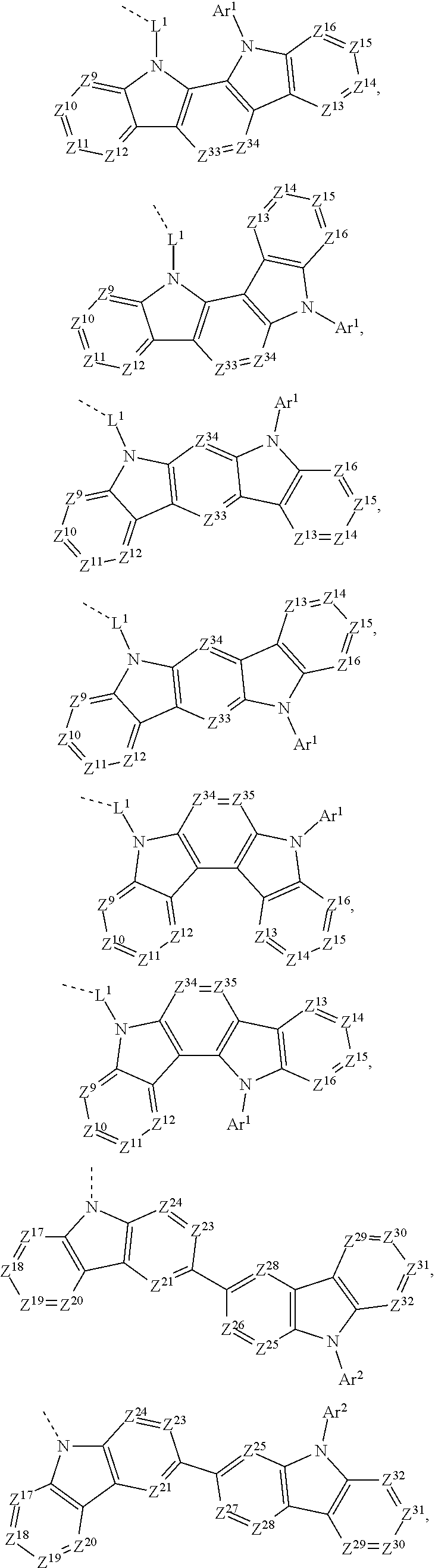
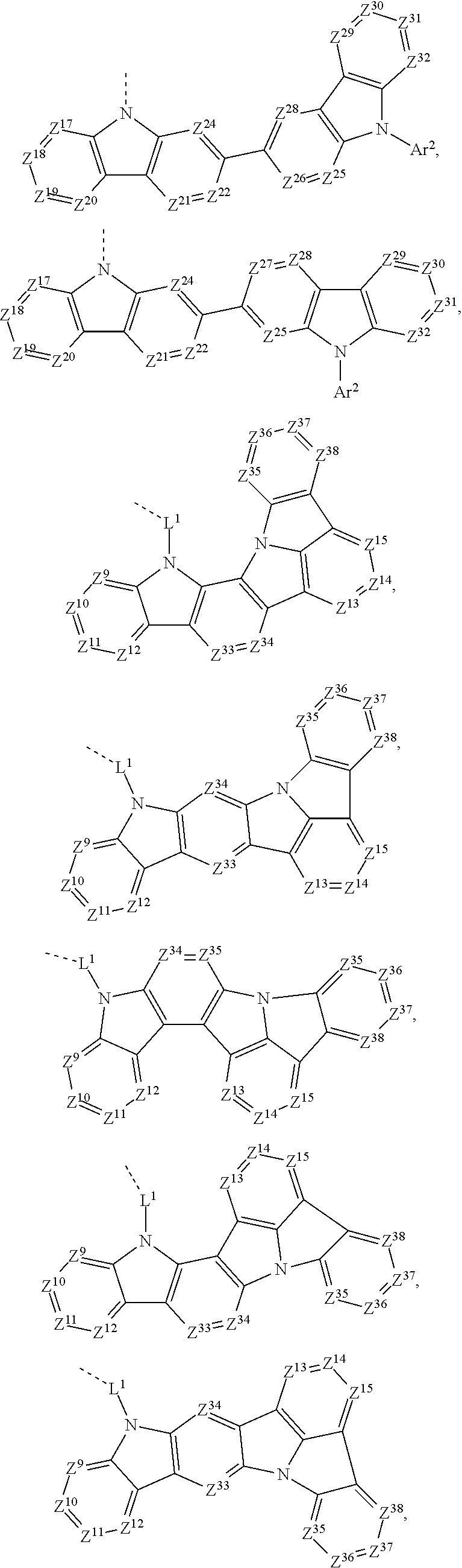
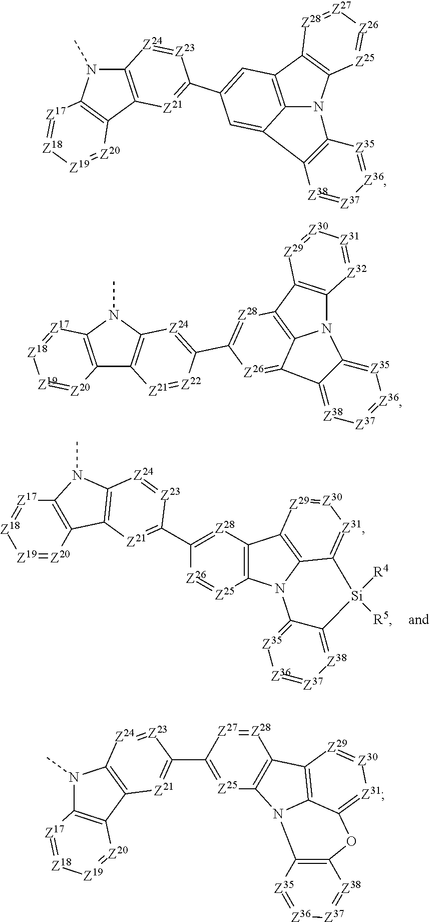
2. The compound of claim 1, wherein G is selected from the group consisting of: ##STR00132## ##STR00133## ##STR00134## ##STR00135## ##STR00136## wherein Z.sup.33 to Z.sup.38 are each independently selected from the group consisting of N and CR.sup.6.
3. The compound of claim 1, wherein Z.sup.1, Z.sup.2, and Z.sup.4 to Z.sup.32 are each independently a CR.sup.6.
4. The compound of claim 2, wherein Z.sup.1, Z.sup.2, and Z.sup.4 to Z.sup.32 are each independently a CR.sup.6.
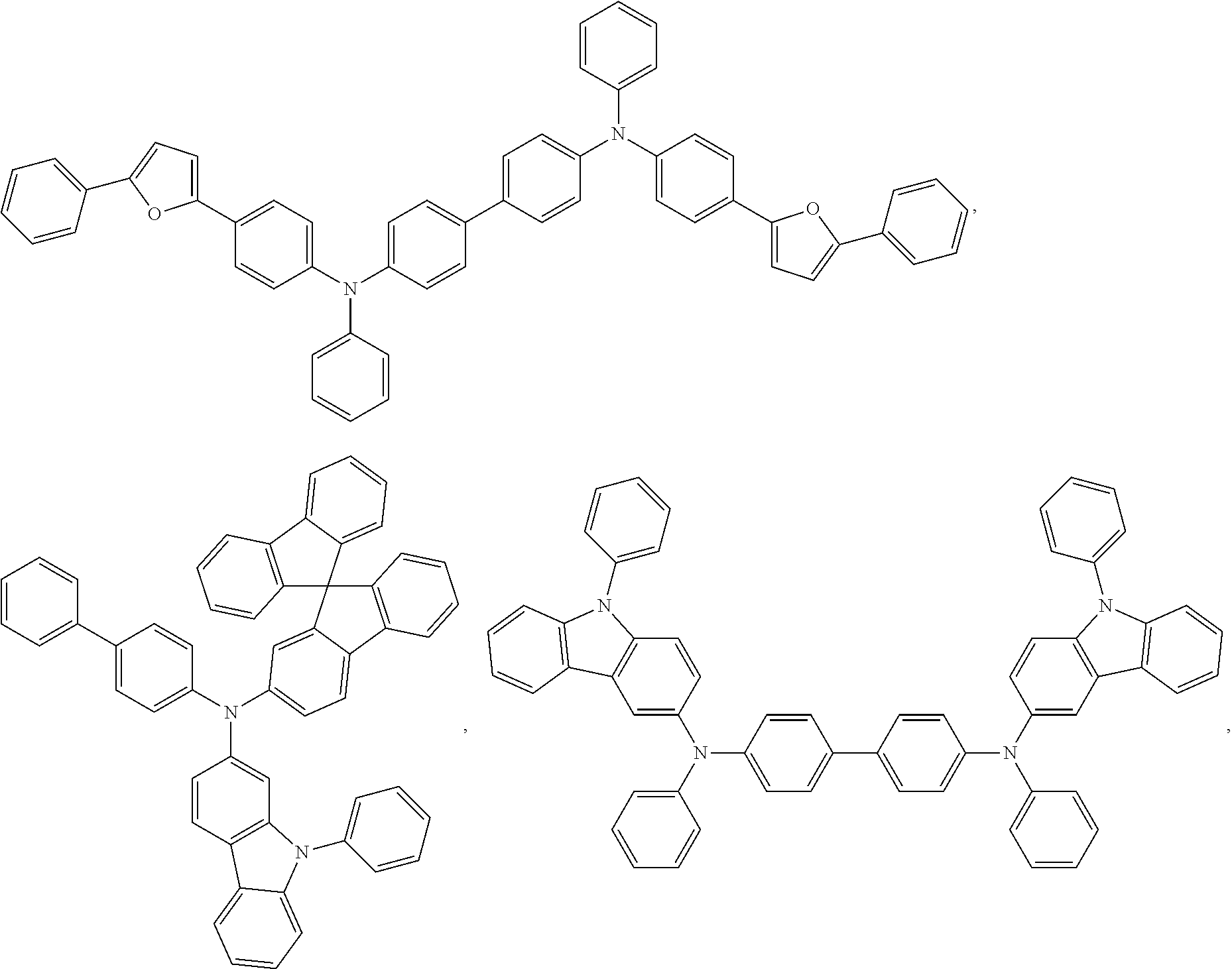
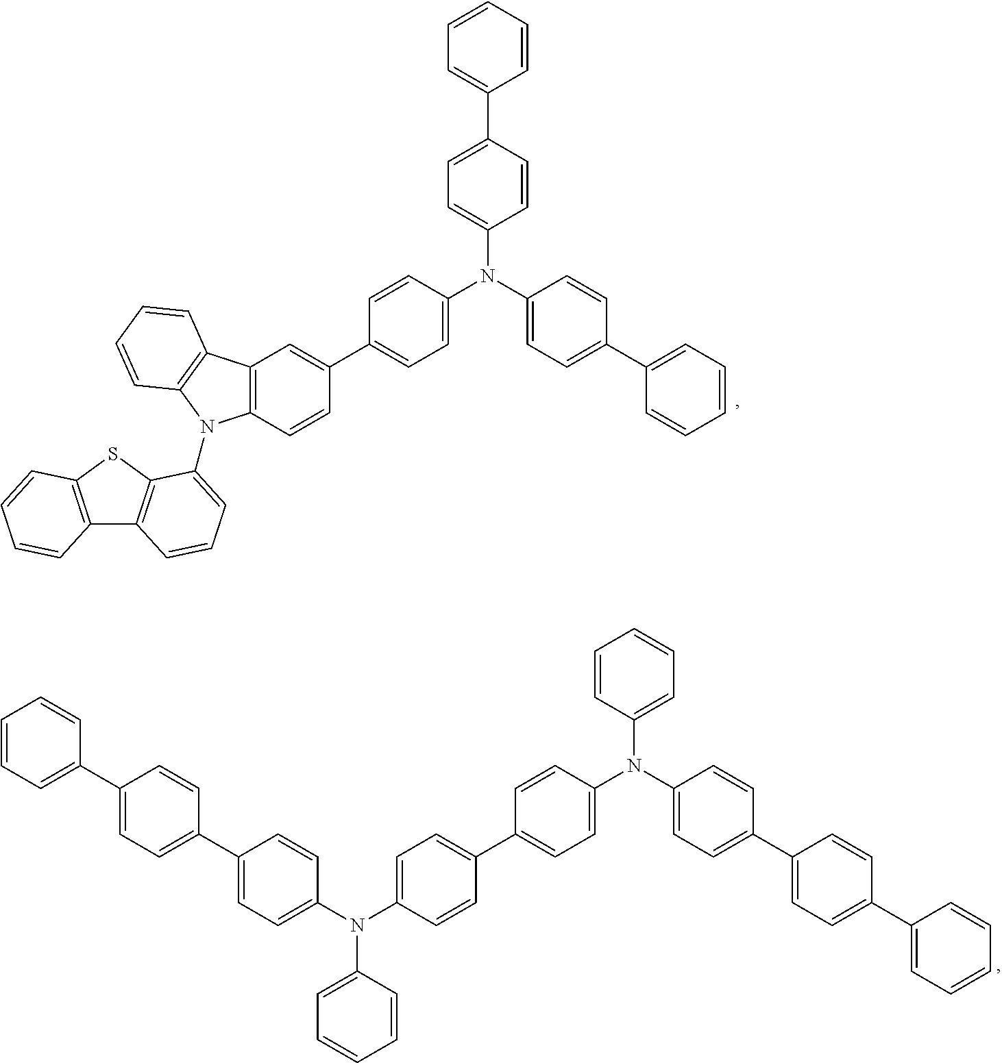
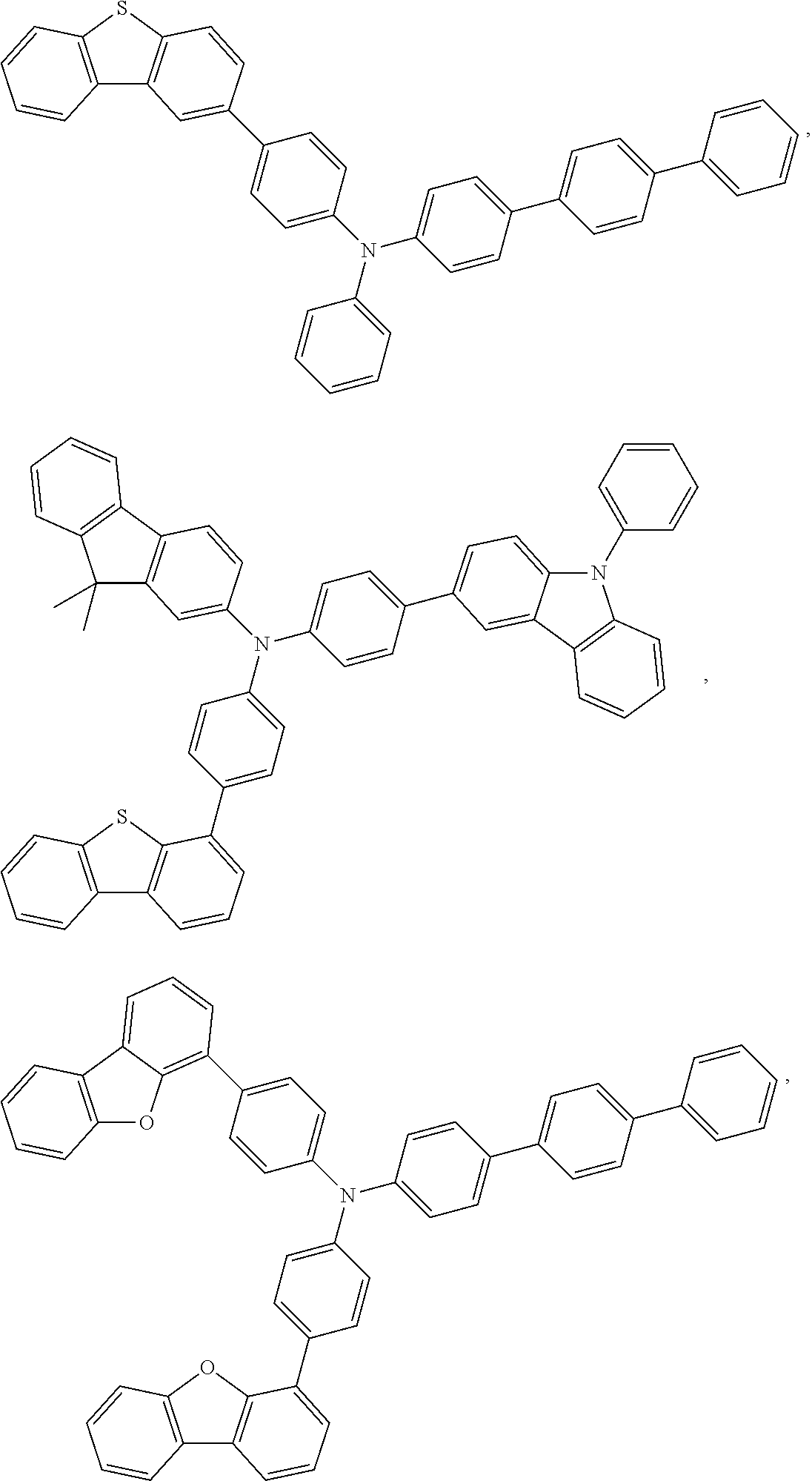
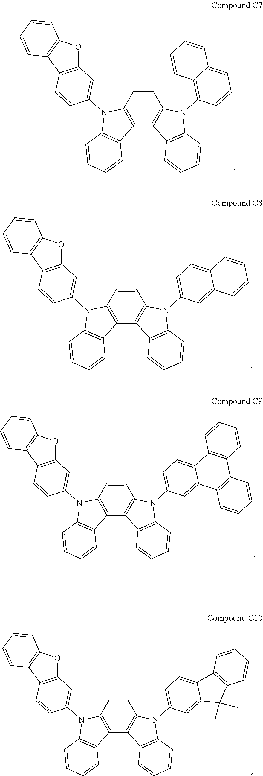
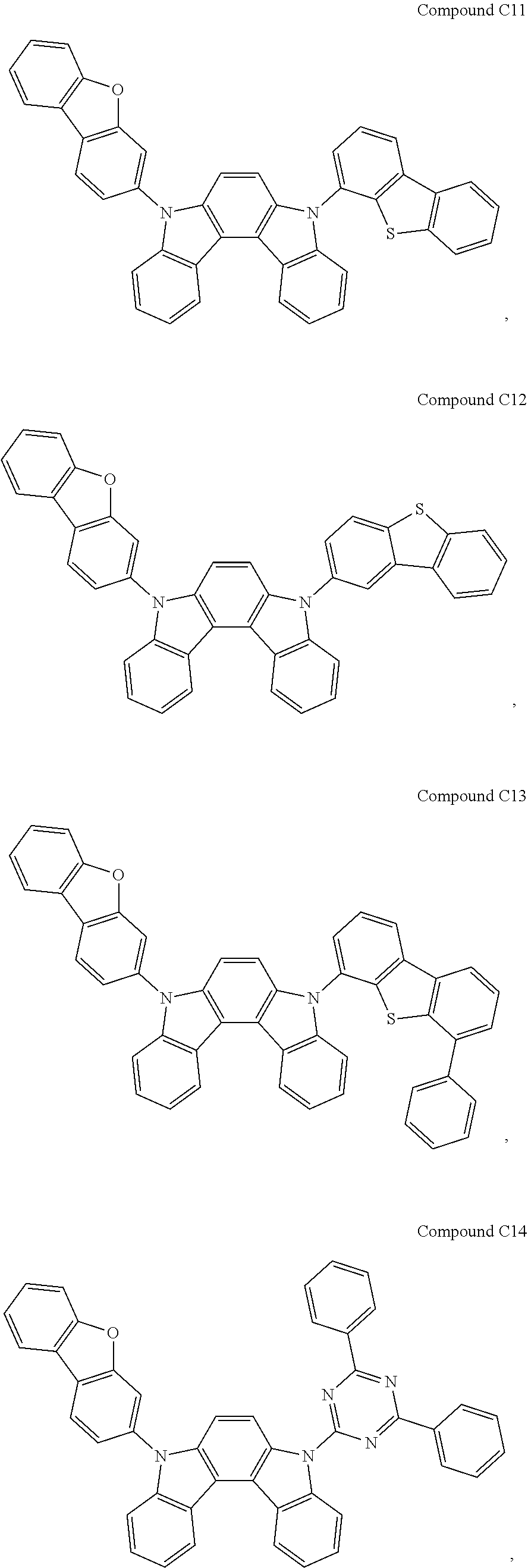
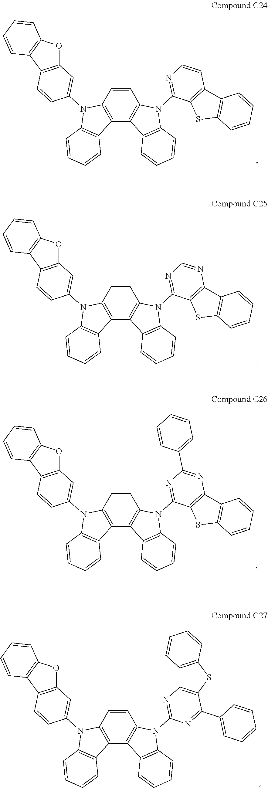
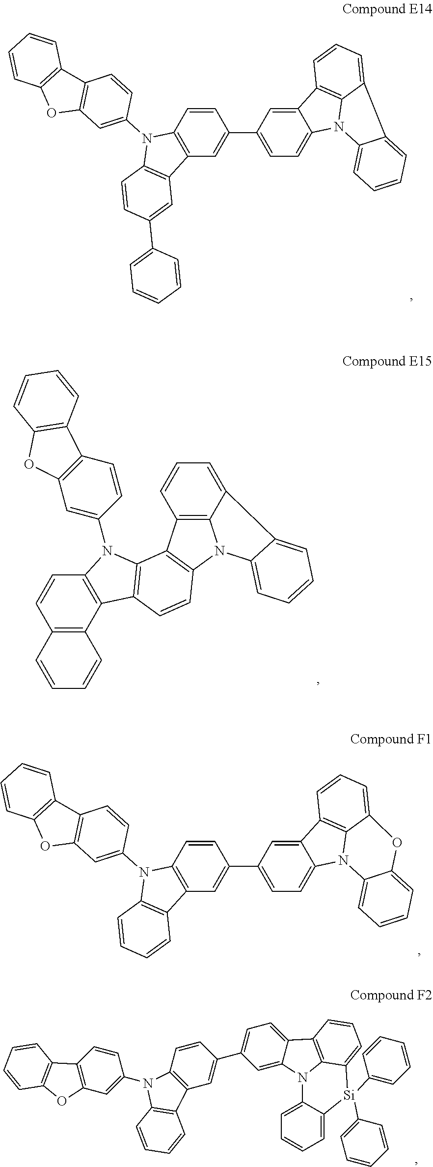
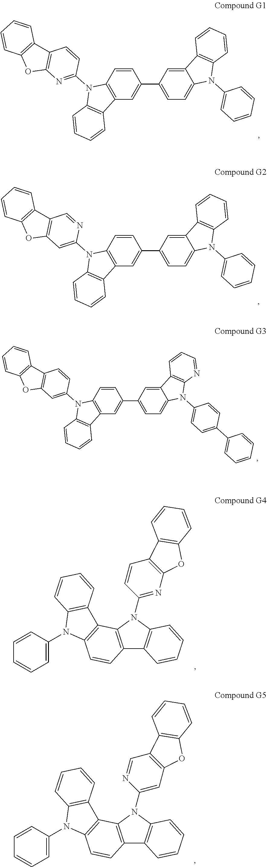
5. The compound of claim 1, wherein the compound is selected from the group consisting of: ##STR00137## ##STR00138## ##STR00139## ##STR00140## ##STR00141## ##STR00142## ##STR00143## ##STR00144## ##STR00145## ##STR00146## ##STR00147## ##STR00148## ##STR00149## ##STR00150## ##STR00151## ##STR00152## ##STR00153## ##STR00154## ##STR00155## ##STR00156## ##STR00157## ##STR00158## ##STR00159## ##STR00160## ##STR00161## ##STR00162## ##STR00163## ##STR00164## ##STR00165## ##STR00166## ##STR00167## ##STR00168##
6. An organic light emitting device (OLED) comprising: an anode; a cathode; and an organic layer, disposed between the anode and the cathode, comprising a compound having Formula I: ##STR00169## wherein G is selected from the group consisting of: ##STR00170## wherein G.sup.1 is a six-member aryl or heteroaryl ring; wherein L.sup.1 is a direct bond or an organic linker; wherein n.sub.1 and n.sub.2 are independently an integer of 0 or 1; when n.sub.1 or n.sub.2 is 0, L.sup.2 or L.sup.3 is not present; and when n.sub.1 or n.sub.2 is 1, L.sup.2 or L.sup.3 is independently selected from the group consisting of a direct bond, oxygen, CR.sup.1R.sup.2, NR.sup.3, and SiR.sup.4R.sup.5; wherein Z.sup.1, Z.sup.2, and Z.sup.4 to Z.sup.32 are each independently selected from the group consisting of N and CR.sup.6; wherein Ar.sup.1 and Ar.sup.2 are each independently selected from the group consisting of aryl and heteroaryl; wherein R.sup.1, R.sup.2, R.sup.3, R.sup.4, and R.sup.5 are each independently selected from the group consisting of hydrogen, deuterium, halogen, alkyl, cycloalkyl, heteroalkyl, arylalkyl, alkoxy, aryloxy, amino, silyl, alkenyl, cycloalkenyl, heteroalkenyl, alkynyl, aryl, heteroaryl, acyl, carbonyl, carboxylic acid, ester, nitrile, isonitrile, sulfanyl, sulfinyl, sulfonyl, phosphino, and combinations thereof, and wherein any two adjacent substituents can optionally join or fuse into a ring; where each R.sup.6 is independently selected from the group consisting of a direct bond, hydrogen, deuterium, halogen, alkyl, cycloalkyl, heteroalkyl, arylalkyl, alkoxy, aryloxy, silyl, alkenyl, cycloalkenyl, heteroalkenyl, alkynyl, aryl, heteroaryl, acyl, carbonyl, carboxylic acid, ester, nitrile, isonitrile, sulfanyl, sulfinyl, sulfonyl, phosphino, and combinations thereof, and wherein any two adjacent substituents can optionally join or fuse into a ring; and wherein G.sup.1, Ar.sup.1, and Ar.sup.2 each can be further substituted by one or more substituents selected from the group consisting of hydrogen, deuterium, halogen, alkyl, cycloalkyl, heteroalkyl, arylalkyl, alkoxy, aryloxy, amino, silyl, alkenyl, cycloalkenyl, heteroalkenyl, alkynyl, aryl, heteroaryl, acyl, carbonyl, carboxylic acid, ester, nitrile, isonitrile, sulfanyl, sulfinyl, sulfonyl, phosphino, and combinations thereof, and wherein any two adjacent substituents can optionally join or fuse into a ring; provided that R.sup.6 does not comprise a carbazole.
7. The OLED of claim 6, wherein the organic layer is an emissive layer and the compound of Formula I is a host.
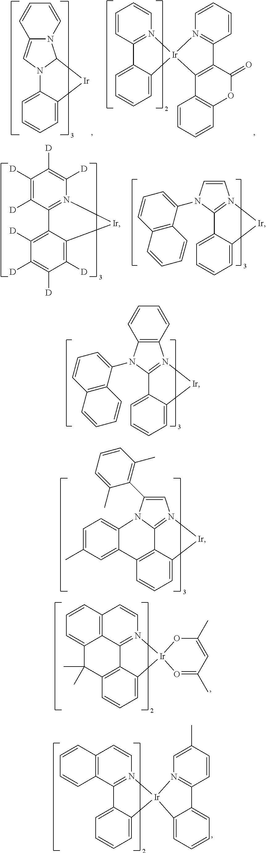
8. The OLED of claim 6, wherein the organic layer further comprises a phosphorescent emissive dopant; wherein the emissive dopant is a transition metal complex having at least one ligand or part of the ligand if the ligand is more than bidentate selected from the group consisting of: ##STR00171## ##STR00172## wherein each X.sup.1 to X.sup.13 are independently selected from the group consisting of carbon and nitrogen; wherein X is selected from the group consisting of BR', NR', PR', O, S, Se, C.dbd.O, S.dbd.O, SO.sub.2, CR'R'', SiR'R'', and GeR'R''; wherein R' and R'' are optionally fused or joined to form a ring; wherein each R.sub.a, R.sub.b, R.sub.c, and R.sub.d may represent from mono substitution to the possible maximum number of substitution, or no substitution; wherein R', R'', R.sub.a, R.sub.b, R.sub.c, and R.sub.d are each independently selected from the group consisting of hydrogen, deuterium, halide, alkyl, cycloalkyl, heteroalkyl, arylalkyl, alkoxy, aryloxy, amino, silyl, alkenyl, cycloalkenyl, heteroalkenyl, alkynyl, aryl, heteroaryl, acyl, carbonyl, carboxylic acids, ester, nitrile, isonitrile, sulfanyl, sulfinyl, sulfonyl, phosphino, and combinations thereof; and wherein any two adjacent substituents of R.sub.a, R.sub.b, R.sub.c, and R.sub.d are optionally fused or joined to form a ring or form a multidentate ligand.
9. The OLED of claim 6, wherein the organic layer is a blocking layer and the compound of Formula I is a blocking material in the organic layer.
10. The OLED of claim 6, wherein the organic layer is a transporting layer and the compound of Formula I is a transporting material in the organic layer.
11. The OLED of claim 6, wherein the OLED is incorporated into a device is selected from the group consisting of a consumer product, an electronic component module, and a lighting panel.
12. A formulation comprising a compound having Formula I: ##STR00173## wherein G is selected from the group consisting of: ##STR00174## wherein G.sup.1 is a six-member aryl or heteroaryl ring; wherein L.sup.1 is a direct bond or an organic linker; wherein n.sub.1 and n.sub.2 are independently an integer of 0 or 1; when n.sub.1 or n.sub.2 is 0, L.sup.2 or L.sup.3 is not present; and when n.sub.1 or n.sub.2 is 1, L.sup.2 or L.sup.3 is independently selected from the group consisting of a direct bond, oxygen, CR.sup.1R.sup.2, NR.sup.3, and SiR.sup.4R.sup.5; wherein Z.sup.1, Z.sup.2, and Z.sup.4 to Z.sup.32 are each independently selected from the group consisting of N and CR.sup.6; wherein Ar.sup.1 and Ar.sup.2 are each independently selected from the group consisting of aryl and heteroaryl; wherein R.sup.1, R.sup.2, R.sup.3, R.sup.4, and R.sup.5 are each independently selected from the group consisting of hydrogen, deuterium, halogen, alkyl, cycloalkyl, heteroalkyl, arylalkyl, alkoxy, aryloxy, amino, silyl, alkenyl, cycloalkenyl, heteroalkenyl, alkynyl, aryl, heteroaryl, acyl, carbonyl, carboxylic acid, ester, nitrile, isonitrile, sulfanyl, sulfinyl, sulfonyl, phosphino, and combinations thereof, and wherein any two adjacent substituents can optionally join or fuse into a ring; where each R.sup.6 is independently selected from the group consisting of a direct bond, hydrogen, deuterium, halogen, alkyl, cycloalkyl, heteroalkyl, arylalkyl, alkoxy, aryloxy, silyl, alkenyl, cycloalkenyl, heteroalkenyl, alkynyl, aryl, heteroaryl, acyl, carbonyl, carboxylic acid, ester, nitrile, isonitrile, sulfanyl, sulfinyl, sulfonyl, phosphino, and combinations thereof, and wherein any two adjacent substituents can optionally join or fuse into a ring; and wherein G.sup.1, Ar.sup.1 , and Ar.sup.2 each can be further substituted by one or more substituents selected from the group consisting of hydrogen, deuterium, halogen, alkyl, cycloalkyl, heteroalkyl, arylalkyl, alkoxy, aryloxy, amino, silyl, alkenyl, cycloalkenyl, heteroalkenyl, alkynyl, aryl, heteroaryl, acyl, carbonyl, carboxylic acid, ester, nitrile, isonitrile, sulfanyl, sulfinyl, sulfonyl, phosphino, and combinations thereof, and wherein any two adjacent substituents can optionally join or fuse into a ring; provided that R.sup.6 does not comprise a carbazole.
Description
CROSS-REFERENCE TO RELATED APPLICATIONS
[0001] This application claims priority from U.S. Provisional Patent Application Ser. Nos. 62/143,370, filed Apr. 6, 2015, 62/245,578, filed Oct. 23, 2015, 62/254,299, filed Nov. 12, 2015, and 62/274,520, filed Jan. 4, 2016, all of which applications are incorporated by reference herein in their entireties.
PARTIES TO A JOINT RESEARCH AGREEMENT
[0002] The claimed invention was trade by, on behalf of, and/or in connection with one or more of the following parties to a joint university corporation research agreement: Regents of the University of Michigan, Princeton University, University of Southern California, and the Universal Display Corporation. The agreement was in effect on and before the date the claimed invention was made, and the claimed invention was made as a result of activities undertaken within the scope of the agreement.
FIELD OF THE INVENTION
[0003] The present invention relates to compounds for use as host materials or electron transporting materials, and devices, such as organic light emitting diodes, including the same.
BACKGROUND
[0004] Opto-electronic devices that make use of organic materials are becoming increasingly desirable for a number of reasons. Many of the materials used to make such devices are relatively inexpensive, so organic opto-electronic devices have the potential for cost advantages over inorganic devices. In addition, the inherent properties of organic materials, such as their flexibility, may make them well suited for particular applications such as fabrication on a flexible substrate. Examples of organic opto-electronic devices include organic light emitting diodes/devices (OLEDs), organic phototransistors, organic photovoltaic cells, and organic photodetectors. For OLEDs, the organic materials may have performance advantages over conventional materials. For example, the wavelength at which an organic emissive layer emits light may generally be readily tuned with appropriate dopants.
[0005] OLEDs make use of thin organic films that emit light when voltage is applied across the device. OLEDs are becoming an increasingly interesting technology for use in applications such as flat panel displays, illumination, and backlighting. Several OLED materials and configurations are described in U.S. Pat. Nos. 5,844,363, 6,303,238, and 5,707,745, which are incorporated herein by reference in their entirety.
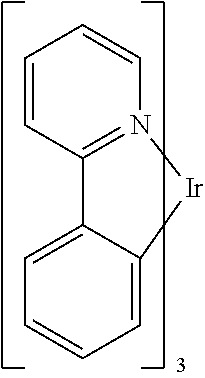
[0006] One application for phosphorescent emissive molecules is a full color display. Industry standards for such a display call for pixels adapted to emit particular colors, referred to as "saturated" colors. In particular, these standards call for saturated red, green, and blue pixels. Alternatively the OLED can be designed to emit white light. In conventional liquid crystal displays emission from a white backlight is filtered using absorption filters to produce red, green and blue emission. The same technique can also be used with OLEDs. The white OLED can be either a single EML device or a stack structure. Color may be measured using CIE coordinates, which are well known to the art.
[0007] One example of a green emissive molecule is tris(2-phenylpyridine)iridium, denoted Ir(ppy).sub.3, which has the following structure:
##STR00001##
[0008] In this, and later figures herein, we depict the dative bond from nitrogen to metal (here, Ir) as a straight line.
[0009] As used herein, the term "organic" includes polymeric materials as well as small molecule organic materials that may be used to fabricate organic opto-electronic devices. "Small molecule" refers to any organic material that is not a polymer, and "small molecules" may actually be quite large. Small molecules may include repeat units in some circumstances. For example, using a long chain alkyl group as a substituent does not remove a molecule from the "small molecule" class. Small molecules may also be incorporated into polymers, for example as a pendent group on a polymer backbone or as a part; of the backbone. Small molecules may also serve as the core moiety of a dendrimer, which consists of a series of chemical shells built on the core moiety. The core moiety of a dendrimer may be a fluorescent or phosphorescent small molecule emitter. A dendrimer may be a "small molecule," and it is believed that all dendrimers currently used in the field of OLEDs are small molecules.
[0010] As used herein, "top" means furthest away from the substrate, while "bottom" means closest to the substrate. Where a first layer is described as "disposed over" a second layer, the first layer is disposed further away from substrate. There may be other layers between the first and second layer, unless it is specified that the first layer is "in contact with" the second layer. For example, a cathode may be described as "disposed over" an anode, even though there are various organic layers in between.
[0011] As used herein, "solution processible" means capable of being dissolved, dispersed, or transported in and/or deposited from a liquid medium, either in solution or suspension form.
[0012] A ligand may be referred to as "photoactive" when it is believed that the ligand directly contributes to the photoactive properties of an emissive material. A ligand may be referred to as "ancillary" when it is believed that the ligand does not contribute to the photoactive properties of an emissive material, although an ancillary ligand may alter the properties of a photoactive ligand.
[0013] As used herein, and as would be generally understood by one skilled in the art, a first "Highest Occupied Molecular Orbital" (HOMO) or "Lowest Unoccupied Molecular Orbital" (LUMO) energy level is "greater than" or "higher than" a second HOMO or LUMO energy level if the first energy level is closer to the vacuum energy level. Since ionization potentials (IP) are measured as a negative energy relative to a vacuum level, a higher HOMO energy level corresponds to an IP having a smaller absolute value (an IP that is less negative). Similarly, a higher LUMO energy level corresponds to an electron affinity (EA) having a smatter absolute value (an EA that is less negative). On a conventional energy level diagram, with the vacuum level at the top, the LUMO energy level of a material is higher than the HOMO energy level of the same material. A "higher" HOMO or LUMO energy level appears closer to the top of such a diagram than a "lower" HOMO or LUMO energy level.
[0014] As used herein, and as would be generally understood by one skilled in the art, a first work function is "greater than" or "higher than" a second work function if the first work function has a higher absolute value. Because work functions are generally measured as negative numbers relative to vacuum level, this means that a "higher" work function is more negative. On a conventional energy level diagram, with the vacuum level at the top, a "higher" work function is illustrated as further away from the vacuum level in the downward direction. Thus, the definitions of HOMO and LUMO energy levels follow a different convention than work functions.
[0015] More details on OLEDs, and the definitions described above, can be found in U.S. Pat. No. 7,279,704, which is incorporated herein by reference in its entirety.
[0016] There is a need in the art for dibenzofuran compounds with improved performance in OLEDs. This invention addresses this need in the art.
SUMMARY
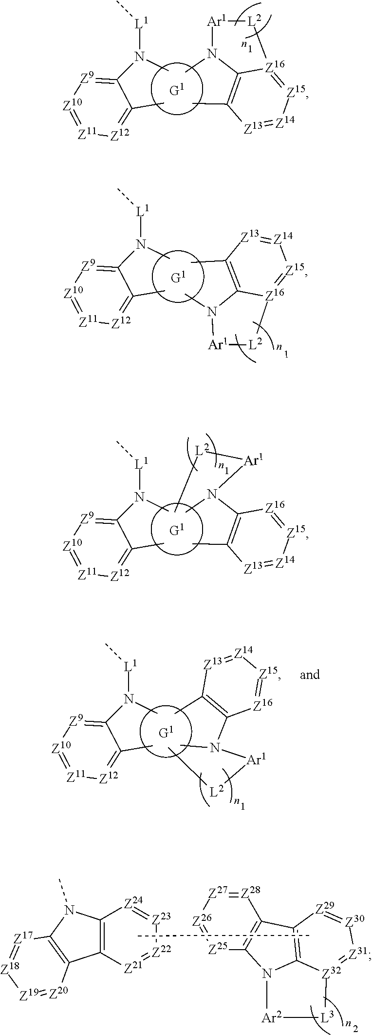
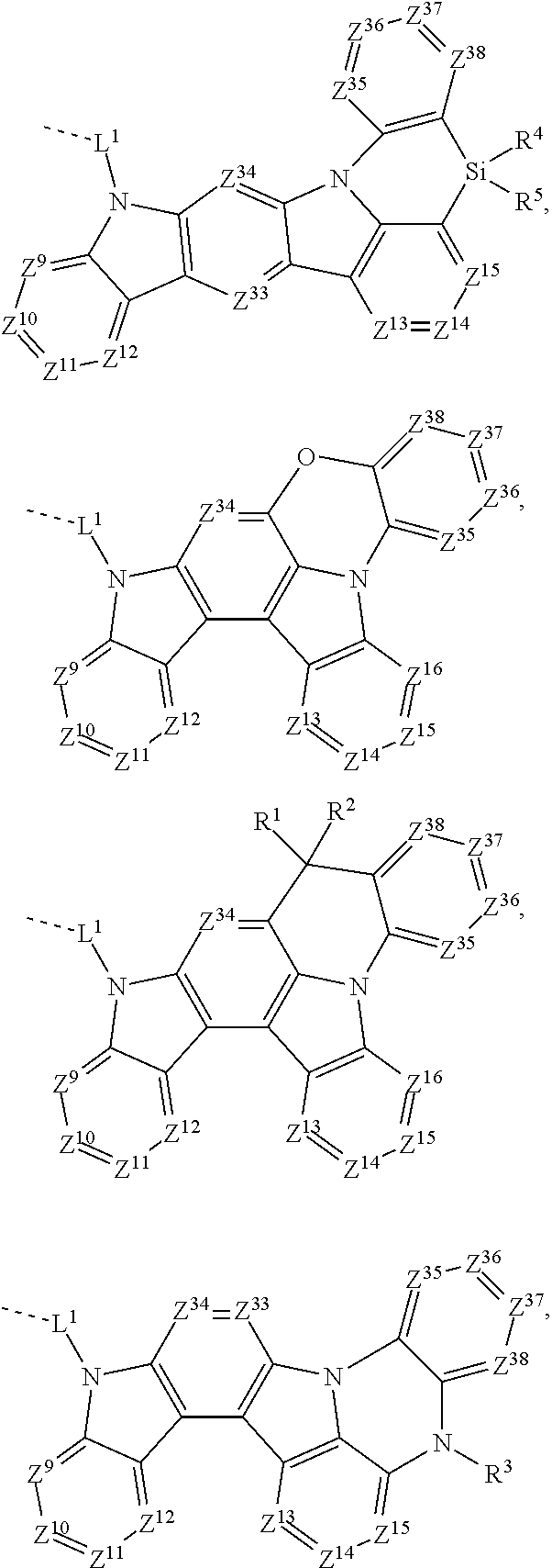
[0017] According to an embodiment, a compound is provided that has the structure of Formula 1 shown below:
##STR00002##
[0018] wherein G is selected from the group consisting of:
##STR00003##
[0019] wherein G.sup.1 is a six-member aryl or heteroaryl ring;
[0020] wherein L.sup.1 is a direct bond or an organic linker;
[0021] wherein n.sub.1 and n.sub.2 are independently an integer of 0 or 1; when n.sub.1 or n.sub.2 is 0, L.sup.2 or L.sup.3 is not present; and when n.sub.1 or n.sub.2 is 1, L.sup.2 or L.sup.3 is independently selected from the group consisting of a direct bond, oxygen, CR.sup.1R.sup.2, NR.sup.3, and SiR.sup.4R.sup.5;
[0022] wherein Z.sup.1, Z.sup.2, and Z.sup.4 to Z.sup.32 are each independently selected from the group consisting of N and CR.sup.6;
[0023] wherein Ar.sup.1 and Ar.sup.2 are each independently selected from the group consisting of aryl and heteroaryl;
[0024] wherein R.sup.1, R.sup.2, R.sup.3, R.sup.4, and R.sup.5 are each independently selected from the group consisting of hydrogen, deuterium, halogen, alkyl, cycloalkyl, heteroalkyl, arylalkyl, alkoxy, aryloxy, amino, silyl, alkenyl, cycloalkenyl, heteroalkenyl, alkynyl, aryl, heteroaryl, acyl, carbonyl, carboxylic acid, ester, nitrile, isonitrile, sulfanyl, sulfinyl, sulfonyl, phosphino, and combinations thereof, and wherein any two adjacent substituents can optionally join or fuse into a ring;
[0025] where each R.sup.6 is independently selected from the group consisting of hydrogen, deuterium, halogen, alkyl, cycloalkyl, heteroalkyl, arylalkyl, alkoxy, aryloxy, silyl, alkenyl, cycloalkenyl, heteroalkenyl, alkynyl, aryl, heteroaryl, acyl, carbonyl, carboxylic acid, ester, nitrile, isonitrile, sulfanyl, sulfinyl, sulfonyl, phosphino, and combinations thereof, and wherein any two adjacent substituents can optionally join or fuse into a ring; and
[0026] wherein G.sup.1, Ar.sup.1, and Ar.sup.2 each can be further substituted by one or more substituents selected from the group consisting of hydrogen, deuterium, halogen, alkyl, cycloalkyl, heteroalkyl, arylalkyl, alkoxy, aryloxy, amino, silyl, alkenyl, cycloalkenyl, heteroalkenyl, alkynyl, heteroaryl, acyl, carbonyl, carboxylic acid, ester, nitrile, isonitrile, sulfanyl, sulfinyl, sulfonyl, phosphino, and combinations thereof, and wherein any two adjacent substituents can optionally join or fuse into a ring;
[0027] provided that R.sup.6 does not comprise a carbazole.
[0028] According to another embodiment, an organic light emitting diode/device (OLED) is also provided. The OLED can include an anode, a cathode, and an organic layer, disposed between the anode and the cathode. The organic layer can include a compound of Formula I. According to yet another embodiment, the organic light emitting device is incorporated into a device selected from a consumer product, an electronic component module, and/or a lighting panel.
[0029] According to another embodiment, the invention provides a formulation comprising a compound of Formula I.
BRIEF DESCRIPTION OF THE DRAWINGS
[0030] FIG. 1 shows an organic light emitting device.
[0031] FIG. 2 shows an inverted organic light emitting device that does not have a separate electron transport: layer.
DETAILED DESCRIPTION
[0032] Generally, an OLED comprises at least one organic layer disposed between and electrically connected to an anode and a cathode. When a current is applied, the anode injects holes and the cathode injects electrons into the organic layer(s). The injected holes and electrons each migrate toward the oppositely charged electrode. When an election and hole localize on the same molecule, an "exciton," which is a localized electron-hole pair having an excited energy state, is formed. Light is emitted when the exciton relaxes via a photoemissive mechanism. In some cases, the exciton may be localized on an excimer or an exciplex. Non-radiative mechanisms, such as thermal relaxation, may also occur, but are generally considered undesirable.
[0033] The initial OLEDs used emissive molecules that emitted light from their singlet states ("fluorescence") as disclosed, for example, in U.S. Pat. No. 4,769,292, which is incorporated by reference in its entirety. Fluorescent emission generally occurs in a time frame of less than 10 nanoseconds.
[0034] More recently, OLEDs having emissive materials that emit light from triplet states ("phosphorescence") have been demonstrated. Baldo et al., "Highly Efficient Phosphorescent Emission from Organic Electroluminescent Devices," Nature, vol. 395, 151-154, 1998; ("Baldo-I") and Baldo et al., "Very high-efficiency green organic light-emitting devices based on electrophosphorescence," Appl. Phys. Lett., vol. 75, No. 3, 4-6 (1999) ("Baldo-II"), are incorporated by reference in their entireties. Phosphorescence is described in more detail in U.S. Pat. No. 7,279,704 at cols. 5-6, which are incorporated by reference.
[0035] FIG. 1 shows an organic light emitting device 100. The figures are not necessarily drawn to scale. Device 100 may include a substrate 110, an anode 115, a hole injection layer 120, a hole transport layer 125, an electron blocking layer 130, an emissive layer 135, a hole blocking layer 140, an electron transport layer 145, an electron injection layer 150, a protective layer 155, a cathode 160, and a barrier layer 170. Cathode 160 is a compound cathode having a first conductive layer 162 and a second conductive layer 164. Device 100 may be fabricated by depositing the layers described, in order. The properties and functions of these various layers, as well as example materials, are described in more detail in U.S. Pat. No. 7,279,704 at cols. 6-10, which are incorporated by reference.
[0036] More examples for each of these layers are available. For example, a flexible and transparent substrate-anode combination is disclosed in U.S. Pat. No. 5,844,363, which is incorporated by reference in its entirety. An example of a p-doped hole transport layer is m-MTDATA doped with F.sub.4-TCNQ at a molar ratio of 50:1, as disclosed in U.S. Patent Application Publication No. 2003/0230980, which is incorporated by reference in its entirety. Examples of emissive and host materials are disclosed in U.S. Pat. No. 6,303,238 to Thompson et al., which is incorporated by reference in its entirety. An example of an n-doped electron transport: layer is BPhen doped with Li at a molar ratio of 1:1, as disclosed in U.S. Patent Application Publication No. 2003/0230980, which is incorporated by reference in its entirety. U.S. Pat. Nos. 5,703,436 and 5,707,745, which are incorporated by reference in their entireties, disclose examples of cathodes including compound cathodes having a thin layer of metal such as Mg:Ag with an overlying transparent, electrically-conductive, sputter-deposited ITO layer. The theory and use of blocking layers is described in more detail in U.S. Pat. No. 6,097,147 and U.S. Patent Application Publication No. 2003/0230980, which are incorporated by reference in their entireties. Examples of injection layers are provided in U.S. Patent Application Publication No. 2004/0174116, which is incorporated by reference in its entirety. A description of protective layers may be found in U.S. Patent Application Publication No. 200410174116, which is incorporated by reference in its entirety.
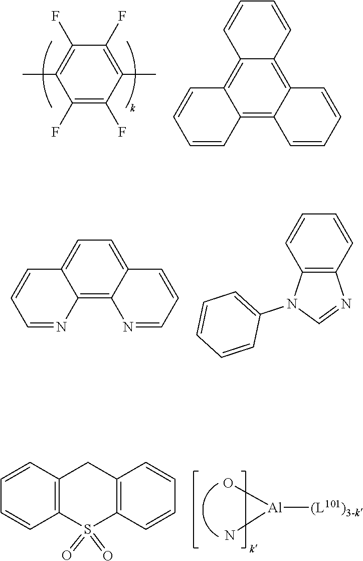
[0037] FIG. 2 shows an inverted OLED 200. The device includes a substrate 210, a cathode 215, an emissive layer 220, a hole transport layer 225, and an anode 230. Device 200 may be fabricated by depositing the layers described, in order. Because the most common OLED configuration has a cathode disposed over the anode, and device 200 has cathode 215 disposed under anode 230, device 200 may be referred to as an "inverted" OLED. Materials similar to those described with respect to device 100 may be used in the corresponding layers of device 200. FIG. 2 provides one example of how some layers may be omitted from the structure of device 100.
[0038] The simple layered structure illustrated in FIGS. 1 and 2 is provided by way of non-limiting example, and it is understood that embodiments of the invention may be used in connection with a wide variety of other structures. The specific materials and structures described are exemplary in nature, and other materials and structures may be used. Functional OLEDs may be achieved by combining the various layers described in different ways, or layers may be omitted entirely, based on design, performance, and cost factors. Other layers not specifically described may also be included. Materials other than those specifically described may be used. Although many of the examples provided herein describe various layers as comprising a single material, it is understood that combinations of materials, such as a mixture of host and dopant, or more generally a mixture, may be used. Also, the layers may have various sublayers. The names given to the various layers herein are not intended to be strictly limiting. For example, in device 200, hole transport layer 225 transports holes and injects holes into emissive layer 220, and may be described as a hole transport layer or a hole injection layer. In one embodiment, an OLED may be described as having an "organic layer" disposed between a cathode and an anode. This organic layer may comprise a single layer, or may further comprise multiple layers of different organic materials as described, for example, with respect to FIGS. 1 and 2.
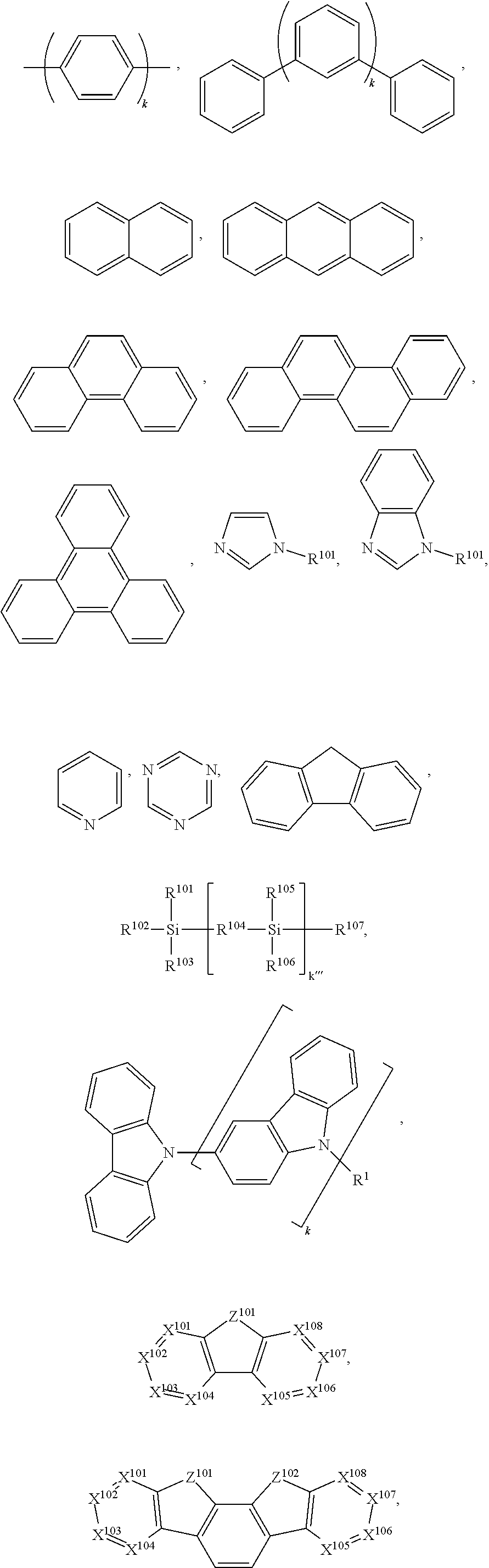
[0039] Structures and materials not specifically described may also be used, such as OLEDs comprised of polymeric materials (PLEDs) such as disclosed in U.S. Pat. No. 5,247,190 to Friend et al., which is incorporated by reference in its entirety. By way of further example, OLEDs having a single organic layer may be used. OLEDs may be stacked, for example as described in U.S. Pat. No. 5,707,745 to Forrest et al, which is incorporated by reference in its entirety. The OLED structure may deviate from the simple layered structure illustrated in FIGS. 1 and 2. For example, the substrate may include an angled reflective surface to improve out-coupling, such as a mesa structure as described in U.S. Pat. No. 6,091,195 to Forrest et al., and/or a pit structure as described in U.S. Pat. No. 5,834,893 to Bulovic et al., which are incorporated by reference in their entireties.
[0040] Unless otherwise specified, any of the layers of the various embodiments may be deposited by any suitable method. For the organic layers, preferred methods include thermal evaporation, ink-jet, such as described in U.S. Pat. Nos. 6,013,982 and 6,087,196, which are incorporated by reference in their entireties, organic vapor phase deposition (OVPD), such as described in U.S. Pat. No. 6,337,102 to Forrest et al., which is incorporated by reference in its entirety, and deposition by organic vapor jet printing (OVJP), such as described in U.S. Pat. No. 7,431,968, which is incorporated by reference in its entirety. Other suitable deposition methods include spin coating and other solution based processes. Solution based processes are preferably carried out in nitrogen or an inert atmosphere. For the other layers, preferred methods include thermal evaporation. Preferred patterning methods include deposition through a mask, cold welding such as described in U.S. Pat. Nos. 6,294,398 and 6,468,819, which are incorporated by reference in their entireties, and patterning associated with some of the deposition methods such as ink-jet and OVJD. Other methods may also be used. The materials to be deposited may be modified to make them compatible with a particular deposition method. For example, substituents such as alkyl and aryl groups, branched or unbranched, and preferably containing at least 3 carbons, may be used in small molecules to enhance their ability to undergo solution processing. Substituents having 20 carbons or more may be used, and 3-20 carbons is a preferred range. Materials with asymmetric structures may have better solution processibility than those having symmetric structures, because asymmetric materials may have a lower tendency to recrystallize. Dendrimer substituents may be used to enhance the ability of small molecules to undergo solution processing.
[0041] Devices fabricated in accordance with embodiments of the present invention may further optionally comprise a barrier layer. One purpose of the barrier layer is to protect the electrodes and organic layers from damaging exposure to harmful species in the environment including moisture, vapor and/or gases, etc. The barrier layer may be deposited over, under or next to a substrate, an electrode, or over any other parts of a device including an edge. The barrier layer may comprise a single layer, or multiple layers. The barrier layer may be formed by various known chemical vapor deposition techniques and may include compositions having a single phase as well as compositions having multiple phases. Any suitable material or combination of materials may be used for the barrier layer. The barrier layer may incorporate an inorganic or an organic compound or both. The preferred barrier layer comprises a mixture of a polymeric material and a non-polymeric material as described in U.S. Pat. No. 7,968,146, PCT Pat. Application Nos. PCT/US2007/023098 and PCT/US2009/042829, which are herein incorporated by reference in their entireties. To be considered a "mixture", the aforesaid polymeric and non-polymeric materials comprising the barrier layer should be deposited under the same reaction conditions and/or at the same time. The weight ratio of polymeric to non-polymeric material may be in the range of 95:5 to 5:95. The polymeric material and the non-polymeric material may be created from the same precursor material. In one example, the mixture of a polymeric material and a non-polymeric material consists essentially of polymeric silicon and inorganic silicon.
[0042] Devices fabricated in accordance with embodiments of the invention can be incorporated into a wide variety of electronic component modules (or units) that can be incorporated into a variety of electronic products or intermediate components. Examples of such electronic products or intermediate components include display screens, lighting devices such as discrete light source devices or lighting panels, etc. that can be utilized by the end-user product manufacturers. Such electronic component modules can optionally include the driving electronics and/or power source(s). Devices fabricated in accordance with embodiments of the invention can be incorporated into a wide variety of consumer products that have one or more of the electronic component modules (or units) incorporated therein. Such consumer products would include any kind of products that include one or more light source(s) and/or one or more of some type of visual displays. Some examples of such consumer products include flat panel displays, computer monitors, medical monitors, televisions, billboards, lights for interior or exterior illumination and/or signaling, heads-up displays, fully or partially transparent displays, flexible displays, laser printers, telephones, cell phones, tablets, phablets, personal digital assistants (PDAs), wearable device, laptop computers, digital cameras, camcorders, viewfinders, micro-displays, 3-D displays, vehicles, a large area wall, theater or stadium screen, or a sign. Various control mechanisms may be used to control devices fabricated in accordance with the present invention, including passive matrix and active matrix. Many of the devices are intended for use in a temperature range comfortable to humans, such as 18 degrees C. to 30 degrees C., and more preferably at room temperature (20-25 degrees C.), but could be used outside this temperature range, for example, from -40 degree C. to +80 degree C.
[0043] The materials and structures described herein may have applications in devices other than OLEDs. For example, other optoelectronic devices such as organic solar cells and organic photodetectors may employ the materials and structures. More generally, organic devices, such as organic transistors, may employ the materials and structures.
[0044] The term "halo," "halogen," or "halide" as used herein includes fluorine, chlorine, bromine, and iodine.
[0045] The term "alkyl" as used herein contemplates both straight and branched chain alkyl radicals. Preferred alkyl groups are those containing from one to fifteen carbon atoms and includes methyl, ethyl, propyl, 1-methylethyl, butyl, 1-methylpropyl, 2-methylpropyl, pentyl 1-methylbutyl, 2-methylbutyl, 3-methylbutyl, 1,1-dimethylpropyl, 1,2-dimethylpropyl, 2,2-dimethylpropyl,and the like. Additionally, the alkyl group may be optionally substituted.
[0046] The term "cycloalkyl" as used herein contemplates cyclic alkyl radicals. Preferred cycloalkyl groups are those containing 3 to 10 ring carbon atoms and includes cyclopropyl, cyclopentyl, cyclohexyl, adamantyl, and the like. Additionally, the cycloalkyl group may be optionally substituted.
[0047] The term "alkenyl" as used herein contemplates both straight and branched chain alkene radicals. Preferred alkenyl groups are those containing two to fifteen carbon atoms. Additionally, the alkenyl group may be optionally substituted.
[0048] The term "alkynyl" as used herein contemplates both straight and branched chain alkyne radicals. Preferred alkynyl groups are those containing two to fifteen carbon atoms. Additionally, the alkynyl group may be optionally substituted.
[0049] The terms "aralkyl" or "arylalkyl" as used herein are used interchangeably and contemplate an alkyl group that has as a substituent an aromatic group. Additionally, the aralkyl group may be optionally substituted.
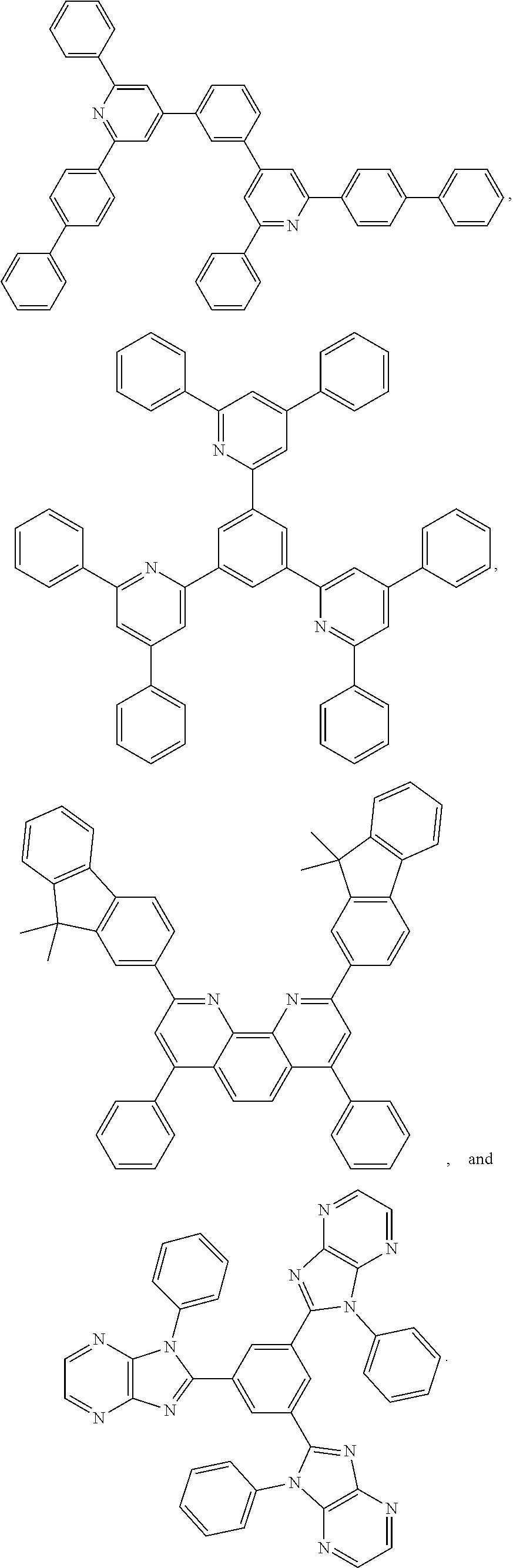
[0050] The term "heterocyclic group" as used herein contemplates aromatic and non-aromatic cyclic radicals. Hetero-aromatic cyclic radicals also means heteroaryl. Preferred hetero-non-aromatic cyclic groups are those containing 3 or 7 ring atoms which includes at least one hetero atom, and includes cyclic amines such as morpholino, piperidino, pyrrolidino, and the like, and cyclic ethers, such as tetrahydrofuran, tetrahydropyran, and the like. Additionally, the heterocyclic group may be optionally substituted.
[0051] The term "aryl" or "aromatic group" as used herein contemplates single-ring groups and polycyclic ring systems. The polycyclic rings may have two or more rings in which two carbons are common to two adjoining rings (the rings are "fused") wherein at least one of the rings is aromatic, e.g., the other rings can be cycloalkyls, cycloalkenyls, aryl, heterocycles, and/or heteroaryls. Preferred aryl groups are those containing six to thirty carbon atoms, preferably six to twenty carbon atoms, more preferably six to twelve carbon atoms. Especially preferred is an aryl group having six carbons, ten carbons or twelve carbons. Suitable aryl groups include phenyl, biphenyl, triphenyl, triphenylene, tetraphenylene, naphthalene, anthracene, phenalene, phenanthrene, fluorene, pyrene, chrysene, perylene, and azulene, preferably phenyl, biphenyl, triphenyl, triphenylene, fluorene, and naphthalene. Additionally, the aryl group may be optionally substituted.
[0052] The term "heteroaryl" as used herein contemplates single-ring hetero-aromatic groups that may include from one to five heteroatoms. The term heteroaryl also includes polycyclic hetero-aromatic systems having two or more rings in which two atoms are common to two adjoining rings (the rings are "fused") wherein at least one of the rings is a heteroaryl, e.g., the other rings can be cycloalkyls, cycloalkenyls, aryl, heterocycles, and/or heteroaryls. Preferred heteroaryl groups are those containing three to thirty carbon atoms, preferably three to twenty carbon atoms, more preferably three to twelve carbon atoms. Suitable heteroaryl groups include dibenzothiophene, dibenzofuran, dibenzoselenophene, furan, thiophene, benzofuran, benzothiophene, benzoselenophene, carbazole, indolocarbazole, pyridylindole, pyrrolodipyridine, pyrazole, imidazole, triazole, oxazole, thiazole, oxadiazole, oxatriazole, dioxazole, thiadiazole, pyridine, pyridazine, pyrimidine, pyrazine, triazine, oxazine, oxathiazine, oxadiazine, indole, benzimidazole, indazole, indoxazine, benzoxazole, benzisoxazole, benzothiazole, quinoline, isoquinoline, cinnoline, quinazoline, quinoxaline, naphthyridine, phthalazine, pteridine, xanthene, acridine, phenazine, phenothiazine, phenoxazine, benzofuropyridine, furodipyridine, benzothienopyridine, thienodipyridine, benzoselenophenopyridine, and selenophenodipyridine, preferably dibenzothiophene, dibenzofuran, dibenzoselenophene, carbazole, indolocarbazole, imidazole, pyridine, triazine, benzimidazole, and aza-analogs thereof. Additionally, the heteroaryl group may be optionally substituted.
[0053] The alkyl, cycloalkyl, alkenyl, alkynyl, aralkyl, heterocyclic group, aryl, and heteroaryl may be unsubstituted or may be substituted with one or more substituents selected from the group consisting of deuterium, halogen, alkyl, cycloalkyl, heteroalkyl, arylalkyl, alkoxy, aryloxy, amino, cyclic amino, silyl, alkenyl, cycloalkenyl, heteroalkenyl, alkynyl, aryl, heteroaryl, acyl, carbonyl, carboxylic acid, ether, ester, nitrile, sulfanyl, sulfinyl, sulfonyl, phosphino, and combinations thereof.
[0054] As used herein, "substituted" indicates that a substituent other than H is bonded to the relevant position, such as carbon. Thus, for example, where R.sup.1 is mono-substituted, then one R.sup.1 must be other than H. Similarly, where R.sup.1 is di-substituted, then two of R.sup.1 must be other than H. Similarly, where R.sup.1 is unsubstituted, R.sup.1 is hydrogen for all available positions.
[0055] The "aza" designation in the fragments described herein, i.e. aza-dibenzofuran, aza-dibenzothiophene, etc. means that one or more of the C--H groups in the respective fragment can be replaced by a nitrogen atom, for example, and without any limitation, azatriphenylene encompasses both dibenzo[f,h]quinoxaline and dibenzo[f,h]quinoline. One of ordinary skill in the art can readily envision other nitrogen analogs of the aza-derivatives described above, and all such analogs are intended to be encompassed by the terms as set forth herein.
[0056] It is to be understood that when a molecular fragment is described as being a substituent or otherwise attached to another moiety, its name may be written as if it were a fragment (e.g. phenyl, phenylene, naphthyl, dibenzofuryl) or as if it were the whole molecule (e.g. benzene, naphthalene, dibenzofuran). As used herein, these different ways of designating a substituent or attached fragment are considered to be equivalent.
[0057] The present invention is based in part on dibenzofuran (DBF) compounds comprising bicarbazole or indolocarbazole connected at the 3-position of DBF, providing materials with exceptional performance in OLEDs.
[0058] In one aspect, the present invention includes a compound having Formula I:
##STR00004##
[0059] wherein G is selected from the group consisting of:
##STR00005##
[0060] wherein G.sup.1 is a six-member aryl or heteroaryl ring;
[0061] wherein L.sup.1 is a direct bond or an organic linker;
[0062] wherein n.sub.1 and n.sub.2 are independently an integer of 0 or 1; when n.sub.1 or n.sub.2 is 0, L.sup.2 or L.sup.3 is not present; and when n.sub.1 or n.sub.2 is 1, L.sup.2 or L.sup.3 is independently selected from the group consisting of a direct bond, oxygen, CR.sup.1R.sup.2, NR.sup.3, and SiR.sup.4R.sup.5;
[0063] wherein Z.sup.1, Z.sup.2, and Z.sup.4 to Z.sup.32 are each independently selected from the group consisting of N and CR.sup.6;
[0064] wherein Ar.sup.1 and Ar.sup.2 are each independently selected from the group consisting of aryl and heteroaryl;
[0065] wherein R.sup.1, R.sup.2, R.sup.3, R.sup.4, and R.sup.5 are each independently selected from the group consisting of hydrogen, deuterium, halogen, alkyl, cycloalkyl, heteroalkyl, arylalkyl, alkoxy, aryloxy, amino, silyl, alkenyl, cycloalkenyl, heteroalkenyl, alkynyl, aryl, heteroaryl, acyl, carbonyl, carboxylic acid, ester, nitrile, isonitrile, sulfanyl, sulfinyl, sulfonyl, phosphino, and combinations thereof, and wherein any two adjacent substituents can optionally join or fuse into a ring;
[0066] where each R.sup.6 is independently selected from the group consisting of hydrogen, deuterium, halogen, alkyl, cycloalkyl, heteroalkyl, arylalkyl, alkoxy, aryloxy, silyl, alkenyl, cycloalkenyl, heteroalkenyl, alkynyl, aryl, heteroaryl, acyl, carbonyl, carboxylic acid, ester, nitrile, isonitrile, sulfanyl, sulfinyl, sulfonyl, phosphino, and combinations thereof, and wherein any two adjacent substituents can optionally join or fuse into a ring; and
[0067] wherein G.sup.1, Ar.sup.1, and Ar.sup.2 each can be further substituted by one or more substituents selected from the group consisting of hydrogen, deuterium, halogen, alkyl, cycloalkyl, heteroalkyl, arylalkyl, alkoxy, aryloxy, amino, silyl, alkenyl, cycloalkenyl, heteroalkenyl, alkynyl, aryl, heteroaryl, acyl, carbonyl, carboxylic acid, ester, nitrile, isonitrile, sulfanyl, sulfinyl, sulfonyl, phosphino, and combinations thereof, and wherein any two adjacent substituents can optionally join or fuse into a ring;
[0068] provided that R.sup.6 does not comprise a carbazole.
[0069] G.sup.1 may be any six-member aromatic ring, as would be understood by one of ordinary skill in the art. In one embodiment, G.sup.1 is selected from the group consisting of phenyl and pyridiyl.
[0070] In one embodiment, G is selected from the group consisting of:
##STR00006## ##STR00007## ##STR00008## ##STR00009## ##STR00010## ##STR00011## ##STR00012##
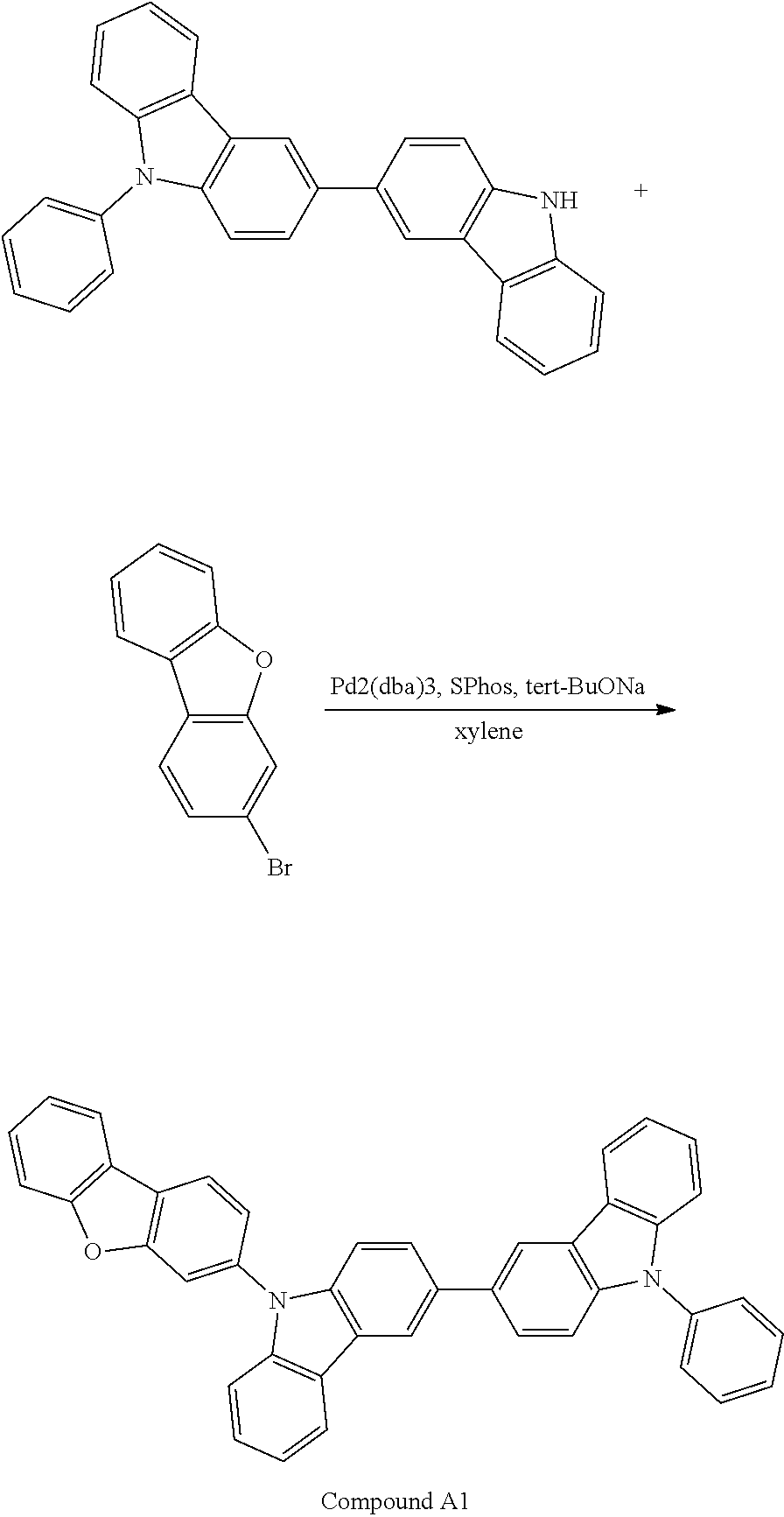
[0071] wherein Z.sup.33 to Z.sup.38 are each independently selected from the group consisting of N and CR.sup.6.
[0072] In one embodiment, Z.sup.1, Z.sup.2, and Z.sup.4 to Z.sup.32 are each independently a CR.sup.6. In another embodiment, Z.sup.1, Z.sup.2, and Z.sup.4 to Z.sup.38 are each independently a CR.sup.6.
[0073] In one embodiment, the compound of the invention is selected from the group consisting of:
##STR00013## ##STR00014## ##STR00015## ##STR00016## ##STR00017## ##STR00018## ##STR00019## ##STR00020## ##STR00021## ##STR00022## ##STR00023## ##STR00024## ##STR00025## ##STR00026## ##STR00027## ##STR00028## ##STR00029## ##STR00030## ##STR00031## ##STR00032## ##STR00033## ##STR00034## ##STR00035## ##STR00036## ##STR00037## ##STR00038## ##STR00039## ##STR00040## ##STR00041## ##STR00042## ##STR00043## ##STR00044##
[0074] In some embodiments, the compound can be an emissive dopant. In some embodiments, the compound can produce emissions via phosphorescence, fluorescence, thermally activated delayed fluorescence, i.e., TADF (also referred to as E-type delayed fluorescence), triplet-triplet annihilation, or combinations of these processes.
[0075] According to another aspect of the present disclosure, an OLED is also provided. The OLED includes an anode, a cathode, and an organic layer disposed between the anode and the cathode. The organic layer may include a host and a phosphorescent dopant. The organic layer can include a compound according to Formula I, and its variations as described herein.
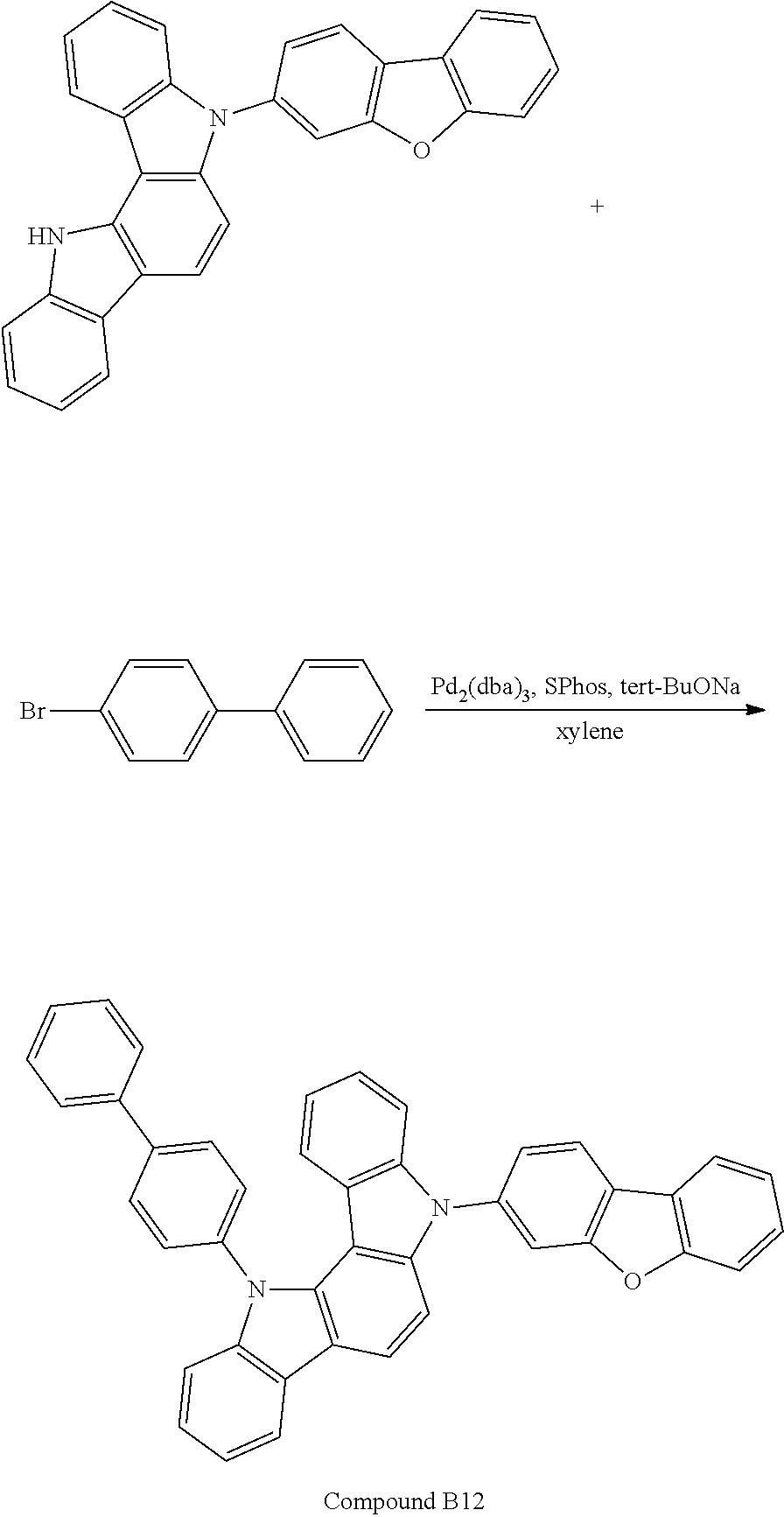
[0076] The OLED can be incorporated into one or more of a consumer product, an electronic component module and a lighting panel. The organic layer can be an emissive layer and the compound can be a host in some embodiments.
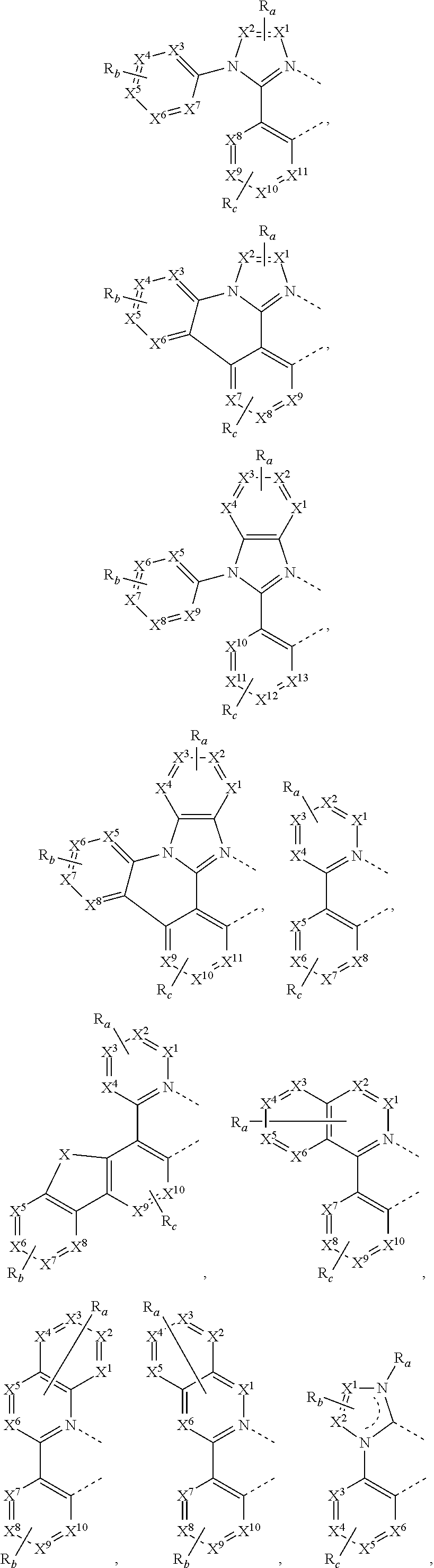
[0077] The organic layer can also include an emissive dopant. In some embodiments, two or more emissive dopants are preferred. In one embodiment, the organic layer further comprises a phosphorescent emissive dopant. In some embodiments the emissive dopant is a transition metal complex having at least one ligand or part of the ligand if the ligand is more than bidentate selected from the group consisting of:
##STR00045## ##STR00046##
[0078] wherein each X.sup.1 to X.sup.13 are independently selected from the group consisting of carbon and nitrogen;
[0079] wherein X is selected from the group consisting of BR', NR', PR', O, S, Se, C.dbd.O, S.dbd.O, SO.sub.2, CR'R'', SiR'R'', and GeR'R'';
[0080] wherein R' and R'' are optionally fused or joined to form a ring;
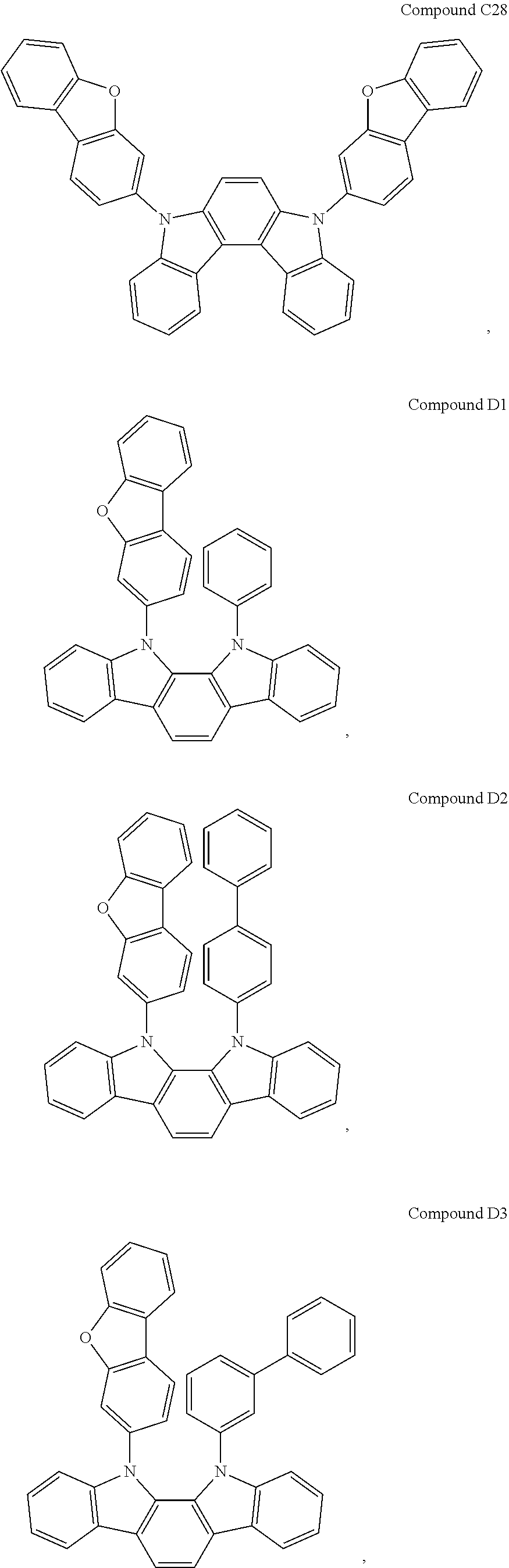
[0081] wherein each R.sub.a, R.sub.b, R.sub.c, and R.sub.d may represent from mono substitution to the possible maximum number of substitution, or no substitution;
[0082] wherein R', R'', R.sub.a, R.sub.b, R.sub.c, and R.sub.d are each independently selected from the group consisting of hydrogen, deuterium, halide, alkyl, cycloalkyl, heteroalkyl, arylalkyl, alkoxy, aryloxy, amino, silyl, alkenyl, cycloalkenyl, heteroalkenyl, alkynyl, aryl, heteroaryl, acyl, carbonyl, carboxylic acids, ester, nitrile, isonitrile, sulfanyl, sulfinyl, sulfonyl, phosphine, and combinations thereof; and
[0083] wherein any two adjacent substituents of R.sub.a, R.sub.b, R.sub.c, and R.sub.d are optionally fused or joined to form a ring or form a multidentate ligand.
[0084] Additional information on possible emissive dopants is provided below.
[0085] In some embodiments the organic layer is a blocking layer and the compound of Formula I is a blocking material in the organic layer. In other embodiments the organic layer is a transporting layer and the compound of Formula I is a transporting material in the organic layer.
[0086] In yet another aspect of the present disclosure, a formulation that comprises a compound according to Formula I is described. The formulation can include one or more components selected from the group consisting of a solvent, a host, a hole injection material, hole transport material, and an electron transport layer material, disclosed herein.
[0087] Combination with Other Materials
[0088] The materials described herein as useful for a particular layer in an organic light emitting device may be used in combination with a wide variety of other materials present in the device. For example, emissive dopants disclosed herein may be used in conjunction with a wide variety of hosts, transport layers, blocking layers, injection layers, electrodes and other layers that may be present. The materials described or referred to below are non-limiting examples of materials that may be useful in combination with the compounds disclosed herein, and one of skill in the art can readily consult the literature to identify other materials that may be useful in combination.
[0089] Conductivity Dopants:
[0090] A charge transport layer can be doped with conductivity dopants to substantially alter its density of charge carriers, which will in turn alter its conductivity. The conductivity is increased by generating charge carriers in the matrix material, and depending on the type of dopant, a change in the Fermi level of the semiconductor may also be achieved. Hole-transporting layer can be doped by p-type conductivity dopants and n-type conductivity dopants are used in the electron-transporting layer. Non-limiting examples of the conductivity dopants that may be used in an OLED in combination with materials disclosed herein are exemplified below together with references that disclose those materials:
[0091] EP01617493, EP01968131, EP2020694, EP2684932, US20050139810, US20070160905, US20090167167, US2010288362, WO06081780, WO2009003455, WO2009008277, WO2009011327, WO2014009310, US2007252140, US2015060804 and US2012146012.
##STR00047## ##STR00048## ##STR00049##
[0092] HIL/HTL:
[0093] A hole injecting/transporting material to be used in the present invention is not particularly limited, and any compound may be used as long as the compound is typically used as a hole injecting/transporting material. Examples of the material include, but are not limited to: a phthalocyanine or porphyrin derivative; an aromatic amine derivative; an indolocarbazole derivative; a polymer containing fluorohydrocarbon; a polymer with conductivity dopants; a conducting polymer, such as PEDOT/PSS; a self-assembly monomer derived from compounds such as phosphonic acid and silane derivatives; a metal oxide derivative, such as MoO.sub.x; a p-type semiconducting organic compound, such as 1,4,5,8,9,12-Hexaazatriphenylenehexacarbonitrile; a metal complex, and a cross-linkable compounds.
[0094] Examples of aromatic amine derivatives used in HIL or HTL include, but not limit to the following general structures:
##STR00050##
[0095] Each of Ar.sup.1 to Ar.sup.9 is selected from the group consisting of aromatic hydrocarbon cyclic compounds such as benzene, biphenyl, triphenyl, triphenylene, naphthalene, anthracene, phenalene, phenanthrene, fluorene, pyrene, chrysene, perylene, and azulene; the group consisting of aromatic heterocyclic compounds such as dibenzothiophene, dibenzofuran, dibenzoselenophene, furan, thiophene, benzofuran, benzothiophene, benzoselenophene, carbazole, indolocarbazole, pyridylindole, pyrrolodipyridine, pyrazole, imidazole, triazole, oxazole, thiazole, oxadiazole, oxatriazole, dioxazole, thiadiazole, pyridine, pyridazine, pyrimidine, pyrazine, triazine, oxazine, oxathiazine, oxadiazine, indole, benzimidazole, indazole, indoxazine, benzoxazole, benzisoxazole, benzothiazole, quinoline, isoquinoline, cinnoline, quinazoline, quinoxaline, naphthyridine, phthalazine, pteridine, xanthene, acridine, phenazine, phenothiazine, phenoxazine, benzafuropyridine, furodipyridine, benzothienopyridine, thienodipyridine, benzoselenophenopyridine, and selenophenodipyridine; and the group consisting of 2 to 10 cyclic structural units which are groups of the same type or different types selected from the aromatic hydrocarbon cyclic group and the aromatic heterocyclic group and are bonded to each other directly or via at least one of oxygen atom, nitrogen atom, sulfur atom, silicon atom, phosphorus atom, boron atom, chain structural unit and the aliphatic cyclic group. Each Ar may be unsubstituted or may be substituted by a substituent selected from the group consisting of deuterium, halide, alkyl, cycloalkyl, heteroalkyl, arylalkyl, alkoxy, aryloxy, amino, silyl, alkenyl, cycloalkenyl, heteroalkenyl, alkynyl, aryl, heteroaryl, acyl, carbonyl, carboxylic acids, ester, nitrile, isonitrile, sulfanyl, sulfinyl, sulfonyl, phosphino, and combinations thereof.
[0096] In one aspect, Ar.sup.1 to Ar.sup.9 is independently selected from the group consisting of:
##STR00051##
wherein k is an integer from 1 to 20; X.sup.101 to X.sup.108 is C (including CH) or N; Z.sup.101 is Ar.sup.1, O, or S; Ar.sup.1 has the same group defined above.
[0097] Examples of metal complexes used in HIL or HTL include, but are not limited to the following general formula:
##STR00052##
wherein Met is a metal, which can have an atomic weight greater than 40; (Y.sup.101-Y.sup.102) is a bidentate ligand, Y.sup.101 and Y.sup.102 are independently selected from C, N, O, P, and S; L.sup.101 is an ancillary ligand; k' is an integer value from 1 to the maximum number of ligands that may be attached to the metal; and k'+k'' is the maximum number of ligands that may be attached to the metal.
[0098] In one aspect, (Y.sup.101-Y.sup.102) is a 2-phenylpyridine derivative. In another aspect, (Y.sup.101-Y.sup.102) is a carbene ligand. In another aspect, Met is selected from Ir, Pt, Os, and Zn. In a further aspect, the metal complex has a smallest oxidation potential in solution vs. Fc.sup.+/Fc couple less than about 0.6 V.
[0099] Non-limiting examples of the HIL and HTL materials that may be used in an OLED in combination w materials disclosed herein are exemplified below together with references that disclose those materials: CN102702075, DE102012005215, EP01624500, EP01698613, EP01806334, EP01930964, EP01972613, EP01997799, EP02011790, EP02055700, EP02055701, EP1725079, EP2085382; EP2660300, EP650955, JP07-073529, JP2005112765, JP2007091719, JP2008021687, JP2014-009196, KR20110088898, KR20130077473, TW201139402, US06517957, US20020158242, US20030162053, US20050123751, US20060182993, US20060240279, US20070145888, US20070181874, US20070278938, US20080014464, US20080091025, US20080106190, US20080124572, 1US20080145707, US20080220265, US20080233434, US20080303417, US2008107919, US20090115320, US20090167161, US2009066235, US2011007385, US20110163302, US2011240968, US2011278551, US2012205642, US2013241401, US20140117329, US2014183517, U.S. Pat. Nos. 5,061,569, 5,639,914, WO05075451, WO07125714, WO08023550, WO08023759, WO2009145016, WO2010061824, WO2011075644, WO2012177006, WO2013018530, WO2013039073, WO2013087142, WO2013118812, WO2013120577, WO2013157367, WO2013175747, WO2014002873, WO2014015935, WO2014015937, WO2014030872, WO2014030921, WO2014034791, WO2014104514, WO2014157018.
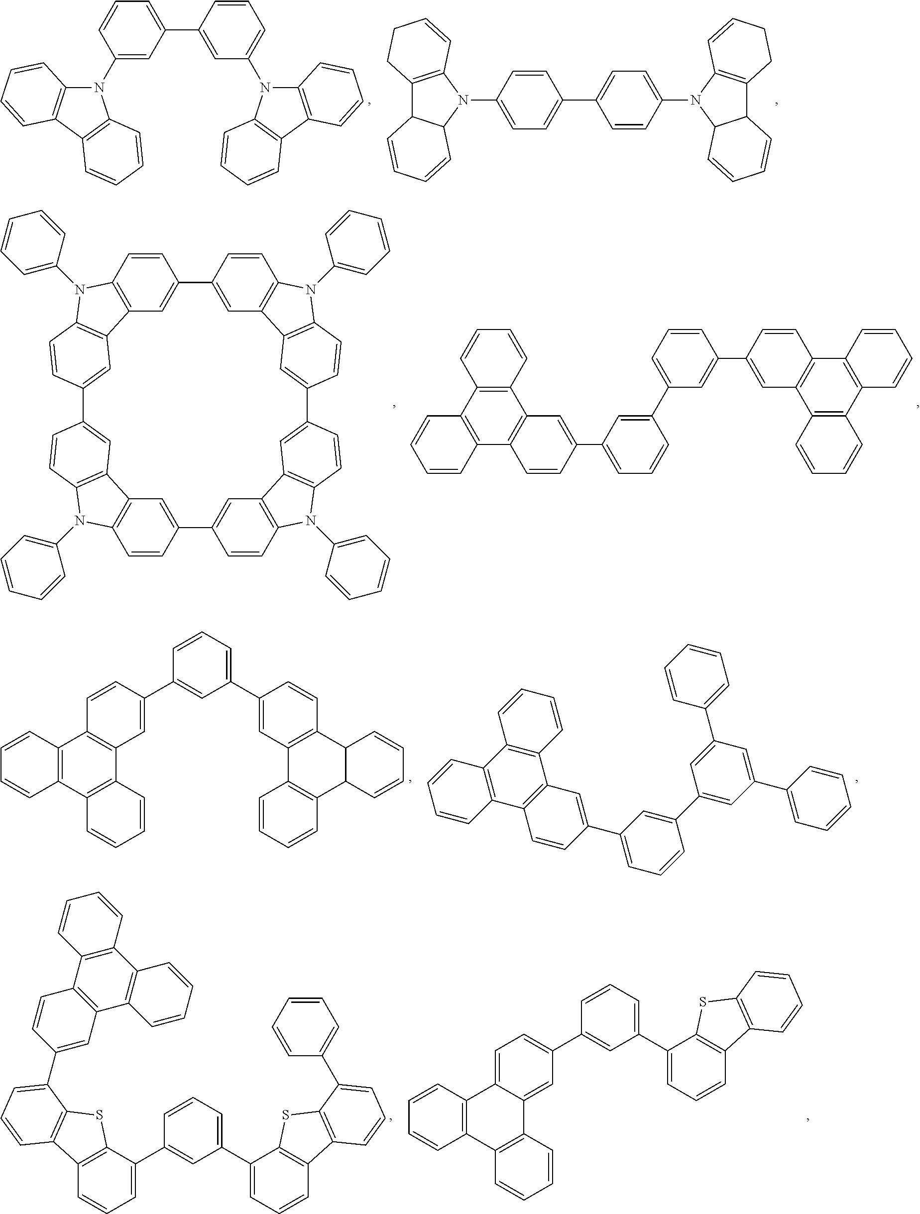
##STR00053## ##STR00054## ##STR00055## ##STR00056## ##STR00057## ##STR00058## ##STR00059## ##STR00060## ##STR00061## ##STR00062## ##STR00063## ##STR00064## ##STR00065## ##STR00066## ##STR00067## ##STR00068## ##STR00069##
[0100] EBL:
[0101] An electron blocking layer (EBL) may be used to reduce the number of electrons and/or excitons that leave the emissive layer. The presence of such a blocking layer in a device may result in substantially higher efficiencies, and or longer lifetime, as compared to a similar device lacking a blocking layer. Also, a blocking layer may be used to confine emission to a desired region of an OLED. In some embodiments, the EBL material has a higher LUMO (closer to the vacuum level) and/or higher triplet energy than the emitter closest to the EBL interface. In some embodiments, the EBL material has a higher LUMO (closer to the vacuum level) and or higher triplet energy than one or more of the hosts closest to the EBL interface. In one aspect, the compound used in EBL contains the same molecule or the same functional groups used as one of the hosts described below.
[0102] Host:
[0103] The light emitting layer of the organic EL device of the present invention preferably contains at least a metal complex as light emitting material, and may contain a host material using the metal complex as a dopant material. Examples of the host material are not particularly limited, and any metal complexes or organic compounds may be used as long as the triplet energy of the host is larger than that of the dopant. While the Table below categorizes host materials as preferred for devices that emit various colors, any host material may be used with dopant so long as the triplet criteria is satisfied.
[0104] Examples of metal complexes used as host are preferred to have the following general formula:
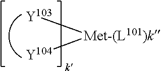
##STR00070##
wherein Met is a metal; (Y.sup.103-Y.sup.104) is a bidentate ligand, Y.sup.103 and Y.sup.104 are independently selected from C, N, O, P, and S; L.sup.101 is an another ligand; k' is an integer value from 1 to the maximum number of ligands that may be attached to the metal; and k'+k'' is the maximum number of ligands that may be attached to the metal.
[0105] In one aspect, the metal complexes are;
##STR00071##
wherein (O--N) is a bidentate ligand, having metal coordinated to atoms O and N.
[0106] In another aspect, Met: is selected from Ir and Pt. In a further aspect, (Y.sup.103-Y.sup.104) is a carbene ligand.
[0107] Examples of organic compounds used as host are selected from the group consisting of aromatic hydrocarbon cyclic compounds such as benzene, biphenyl, triphenyl, triphenylene, tetraphenylene, naphthalene, anthracene, phenalene, phenanthrene, fluorene, pyrene, chrysene, perylene, and azulene; the group consisting of aromatic heterocyclic compounds such as dibenzothiophene, dibenzofuran, dibenzoselenophene, furan, thiophene, benzofuran, benzothiophene, benzoselenophene, carbazole, indolocarbazole, pyridylindole, pyrrolodipyridine, pyrazole, imidazole, triazole, oxazole, thiazole, oxadiazole, oxatriazole, dioxazole, thiadiazole, pyridine, pyridazine, pyrimidine, pyrazine, triazine, oxazine, oxathiazine, oxadiazine, indole, benzimidazole, indazole, indoxazine, benzoxazole, benzisoxazole, benzothiazole, quinoline, isoquinoline, cinnoline, quinazoline, quinoxaline, naphthyridine, phthalazine, pteridine, xanthene, acridine, phenazine, phenothiazine, phenoxazine, benzofuropyridine, furodipyridine, benzothienopyridine, thienodipyridine, benzoselenophenopyridine, and selenophenodipyridine; and the group consisting of 2 to 10 cyclic structural units which are groups of the same type or different types selected from the aromatic hydrocarbon cyclic group and the aromatic heterocyclic group and are bonded to each other directly or via at least one of oxygen atom, nitrogen atom, sulfur atom, silicon atom, phosphorus atom, boron atom, chain structural unit and the aliphatic cyclic group. Each option within each group may be unsubstituted or may be substituted by a substituent selected from the group consisting of deuterium, halide, alkyl, cycloalkyl, heteroalkyl, arylalkyl, alkoxy, aryloxy, amino, silyl, alkenyl, cycloalkenyl, heteroalkenyl, alkynyl, aryl, heteroaryl, acyl, carbonyl, carboxylic acids, ester, nitrile, isonitrile, sulfanyl, sulfinyl, sulfonyl, phosphine, and combinations thereof.
[0108] In one aspect, the host compound contains at least one of the following groups in the molecule:
##STR00072## ##STR00073##
wherein each of R.sup.101 to R.sup.107 is independently selected from the group consisting of hydrogen, deuterium, halide, alkyl, cycloalkyl, heteroalkyl, arylalkyl, alkoxy, aryloxy, amino, silyl, alkenyl, cycloalkenyl, heteroalkenyl, alkynyl, aryl, heteroaryl, acyl, carbonyl, carboxylic acids, ester, nitrile, isonitrile, sulfanyl, sulfinyl, sulfonyl, phosphino, and combinations thereof, and when it is aryl or heteroaryl, it has the similar definition as Ar's mentioned above. k is an integer from 0 to 20 or 1 to 20; k''' is an integer from 0 to 20. X.sup.101 to X.sup.108 is selected from C (including CH) or N. Z.sup.101 and Z.sup.102 is selected from NR.sup.101, O, or S.
[0109] Non-limiting examples of the Host materials that may be used in an OLED in combination with materials disclosed herein are exemplified below together with references that disclose those materials: EP2034538, EP2034538A, EP2757608, JP2007254297, KR20100079458, KR20120088644, KR20120129733, KR20130115564, TW201329200, US20030175553, US20050238919, US20060280965, US20090017330, US20090030202, US20090167162, US20090302743, US20090309488, US20100012931, US20100084966, US20100187984, US2010187984, US2012075273, US2012126221, US2013009543, US2013105787, US2013175519, US2014001446, US20140183503, US20140225088, US2014034914, U.S. Pat. No. 7,154,114, WO2001039234, WO2004093207, WO2005014551, WO2005089025, WO2006072002, WO2006114966, WO2007063754, WO2008056746, WO2009003898, WO2009021126, WO2009063833, WO2009066778, WO2009066779, WO2009086028, WO2010056066, WO2010107244, WO2011081423, WO2011081431, WO2011086863, WO2012128298, WO2012133644, WO2012133649, WO2013024872, WO2013035275, WO2013081315, WO2013191404, WO2014142472.
##STR00074## ##STR00075## ##STR00076## ##STR00077## ##STR00078## ##STR00079## ##STR00080## ##STR00081## ##STR00082## ##STR00083## ##STR00084##
[0110] Emitter:
[0111] An emitter example is not particularly limited, and any compound may be used as long as the compound is typically used as an emitter material. Examples of suitable emitter materials include, but are not limited to, compounds which can produce emissions via phosphorescence, fluorescence, thermally activated delayed fluorescence, i.e., TADF (also referred to as E-type delayed fluorescence), triplet-triplet annihilation, or combinations of these processes.
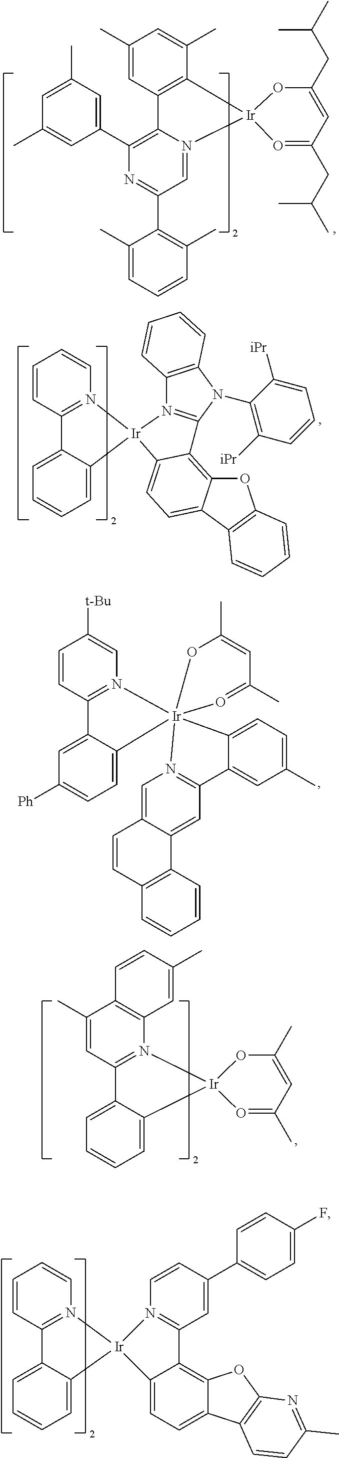
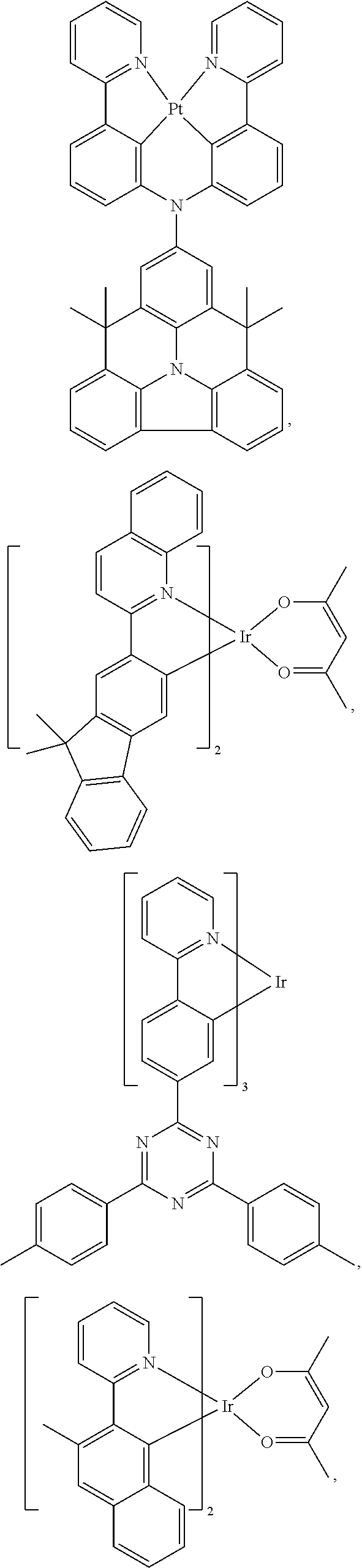
[0112] Non-limiting examples of the emitter materials that may be used in an OLED in combination with materials disclosed herein are exemplified below together with references that disclose those materials: CN103694277, CN1696137, EB01238981, EP01239526, EP01961743, EP1239526, EP1244155, EP1642951, EP1647554, EP1841834, EP1841834B, EP2062907, EP2730583, JP2012074444, JP2013110263, JP4478555, KR1020090133652, KR20120032054, KR20130043460, TW201332980, US06699599, US06916554, US20010019782, US20020034656, US20030068526, US20030072964, US20030138657,US20050123788, US20050244673, US2005123791, US2005260449, US20060008670, US20060065890, US20060127696, US20060134459, US20060134462, US20060202194, US20060251923, US20070034863, US20070087321, US20070103060, US20070111026, US20070190359, US20070231600, US2007034863, US2007104979, US2007104980, US2007138437, US2007224450, US2007278936, US20080020237, US20080233410, US20080261076, US20080297033, US200805851, US2008161567, US2008210930, US20090039776, US20090108737, US20090115322, US20090179555, US2009085476, US2009104472, US20100090591, US20100148663, US20100244004, 1J820100295032, US2010102716, US2010105902, U82010244004, US2010270916, US20110057559, US20110108822, US20110204333, US2011215710, US2011227049, US2011285275, US2012292601, US20130146848, US2013033172, US2013165653, US2013181190, US2013334521, US20140246656, US2014103305, U.S. Pat. Nos. 6,303,238, 6,413,656, 6,653,654, 6,670,645, 6,687,266, 6,835,469, 6,921,915, 7,279,704, 7,332,232, 7,378,162, 7,534,505, 7,675,228, 7,728,137, 7,740,957, 7,759,489, 7,951,947, 8,067,099, 8,592,586, 8,871,361, WO06081973, WO06121811, WO07018067, WO07108362, WO07115970, WO07115981, WO08035571, WO2002015645, WO2003040257, WO2005019373, WO2006056418, WO2008054584, WO2008078800, WO2008096609, WO2008101842, WO2009000673, WO2009050281, WO2009100991, WO2010028151, WO2010054731, WO2010086089, WO2010118029, WO2011044988, WO2011051404, WO2011107491, WO2012020327, WO2012163471, WO2013094620, WO2013107487, WO2013174471, WO2014007565, WO2014008982, WO2014023377, WO2014024131, WO2014031977, WO2014038456, WO2014112450.
##STR00085## ##STR00086## ##STR00087## ##STR00088## ##STR00089## ##STR00090## ##STR00091## ##STR00092## ##STR00093## ##STR00094## ##STR00095## ##STR00096## ##STR00097## ##STR00098## ##STR00099## ##STR00100## ##STR00101## ##STR00102## ##STR00103## ##STR00104## ##STR00105##
[0113] HBL:
[0114] A hole blocking layer (HBL) may be used to reduce the number of holes and/or excitons that leave the emissive layer. The presence of such a blocking layer in a device may result in substantially higher efficiencies and/or longer lifetime as compared to a similar device lacking a blocking layer. Also, a blocking layer may be used to confine emission to a desired region of an OLED. In some embodiments, the HBL material has a lower HOMO (further from the vacuum level) and or higher triplet energy than the emitter closest to the HBL interface. In some embodiments, the HBL material has a lower HOMO (further from the vacuum level) and or higher triplet energy than one or more of the hosts closest to the HBL interface.
[0115] In one aspect, compound used in HBL contains the same molecule or the same functional groups used as host described above.
[0116] In another aspect, compound used in HBL contains at least one of the following groups in the molecule:
##STR00106##
wherein k is an integer from 1 to 20; L.sup.101 is an another ligand, k' is an integer from 1 to 3.
[0117] ETL:
[0118] Electron transport layer (ETL) may include a material capable of transporting electrons. Electron transport layer may be intrinsic (undoped), or doped. Doping may be used to enhance conductivity. Examples of the ETL material are not particularly limited, and any metal complexes or organic compounds may be used as long as they are typically used to transport electrons.
[0119] In one aspect, compound used in ETL contains at least one of the following groups in the molecule:
##STR00107##
[0120] wherein R.sup.101 is selected from the group consisting of hydrogen, deuterium, halide, alkyl, cycloalkyl, heteroalkyl, arylalkyl, alkoxy, aryloxy, amino, silyl, alkenyl, cycloalkenyl, heteroalkenyl, alkynyl, aryl, heteroaryl, acyl, carbonyl, carboxylic acids, ester, nitrile, isonitrile, sulfanyl, sulfinyl, sulfonyl, phosphino, and combinations thereof, when it is aryl or heteroaryl, it has the similar definition as Ar's mentioned above. Ar.sup.1 to Ar.sup.3 has the similar definition as Ar's mentioned above. k is an integer from 1 to 20. X.sup.101 to X.sup.108 is selected from C (including CH) or N.
[0121] In another aspect, the metal complexes used in ETL contains, but not limit to the following general formula:
##STR00108##
wherein (O--N) or (N-N) is a bidentate ligand, having metal coordinated to atoms O, N or N, N; L.sup.101 is another ligand; k' is an integer value from 1 to the maximum number of ligands that may be attached to the metal.
[0122] Non-limiting examples of the ETL materials that may be used in an OLED in combination with materials disclosed herein are exemplified below together with references that disclose those materials: CN103508940, EP01602648, EP01734038, EP01956007, JP2004-022334, JP2005149918, JP2005-268199, KR0117693, KR20130108183, US20040036077, US20070104977, US2007018155, US20090101870, US20090115316, US20090140637, US20090179554, US2009218940, US2010108990, US2011156017, US2011210320, US2012193612, US2012214993, US2014014925, US2014014927, US20140284580, U.S. Pat. Nos. 6,656,612, 8,415,031, WO2003060956, WO2007111263, WO2009148269, WO2010067894, WO2010072300, WO2011074770, WO2011105373, WO2013079217, WO2013145667, WO2013180376, WO2014104499, WO2014104535.
##STR00109## ##STR00110## ##STR00111## ##STR00112## ##STR00113## ##STR00114## ##STR00115## ##STR00116##
[0123] Charge Generation Layer (CGL):
[0124] In tandem or stacked OLEDs, the CGL plays an essential role in the performance, which is composed of an n-doped layer and a p-doped layer for injection of electrons and holes, respectively. Electrons and holes are supplied from the CGL and electrodes. The consumed electrons and holes in the CGL are refilled by the electrons and holes injected from the cathode and anode, respectively; then, the bipolar currents reach a steady state gradually. Typical CGL materials include n and p conductivity dopants used in the transport layers.
[0125] In any above-mentioned compounds used in each layer of the OLED device, the hydrogen atoms can be partially or fully deuterated. Thus, any specifically listed substituent, such as, without limitation, methyl, phenyl, pyridyl, etc. may be undeuterated, partially deuterated, and fully deuterated versions thereof. Similarly, classes of substituents such as, without limitation, alkyl, aryl, cycloalkyl, heteroaryl, etc. also may be undeuterated, partially deuterated, and fully deuterated versions thereof.
EXPERIMENTAL
[0126] Materials Synthesis
[0127] Chemical abbreviations used throughout this document are as follows:
[0128] Pd.sub.2(dba).sub.3 is tri(dibenzylideneacetone) dipalladium(0),
[0129] SPhos is dicyclohexyl(2',6'-dimethoxy-[1,1'-biphenyl]-2-yl)phosphine, and
[0130] XPhos is dicyclohexyl(2',4',6'-triisopropyl-[1,1'-biphenyl]-2-yl)phosphine
[0131] Compound A1
##STR00117##
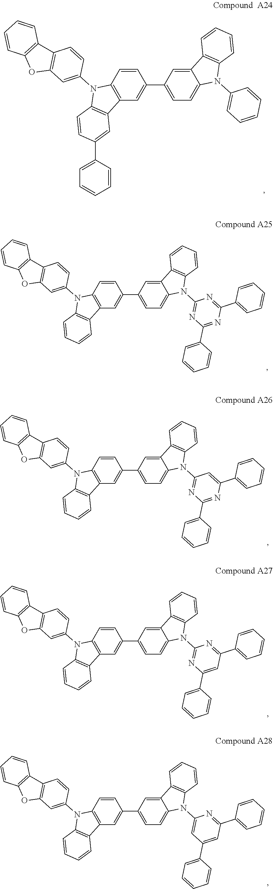
[0132] A solution of 3-bromodibenzo[b,d]furan (2.8 g, 11.33 mmol), 9-phenyl-9H,9'H-3,3'-bicarbazole (4.63 g, 11.33 mmol), Pd.sub.2(dba).sub.3 (0.21 g, 0.23 mmol), SPhos (0.13 g, 0.32 mmol) and tert-BuONa (1.63 g, 17.0 mmol) in xylene (150 ml) was refluxed under nitrogen overnight. Upon evaporation of the solvent, the residue was purified by column chromatography on silica gel with heptane/ethyl acetate (95/5 to 90/10, v/v) as eluent and recrystallized from heptane to yield Compound A1 (5.6 g, 86%) as a white solid.
[0133] Compound A2
##STR00118##
[0134] The procedure for the synthesis of Compound A1 was followed to synthesize Compound A2 from 3-bromodibenzo[b,d]furan and 9-([1,1'-biphenyl]-4-yl)-9H,9'H-3,3'-bicarbazole. Compound A2 was prepared as a white solid in a yield of 93%.
[0135] Compound B1
##STR00119##
[0136] The procedure for the synthesis of Compound A1 was followed to synthesize Compound B1 from 5-phenyl-5,12-dihydroindolo[3,2-.alpha.]carbazole and 3-bromodibenzo[b,d]furan. Compound B1 was prepared as a white solid in a yield of 39%.
[0137] Compound B12
##STR00120##
[0138] A solution of 5,12-dihydroindolo[3,2-a]carbazole (6 g, 23.41 mmol), 3-bromodibenzo[b,d]furan (6.94 g, 28.1 mmol), Pd.sub.2(dba).sub.3 (0.21 g, 0.23 mmol), Xphos (0.23 g, 0.47 mmol) and K.sub.3PO.sub.4 (9.94 g, 46.8 mmol) in toluene (100 ml) was refluxed under nitrogen for 12 h. After cooling to room temperature, the solvent was evaporated and the residue was purified by column chromatography on silica gel with heptane/dichloromethane (1/1, v/v) as eluent to yield 5-(dibenzo[b,d]furan-3-yl)-5,12-dihydroindolo[3,2-a]carbazole (6.3 g, 64%) as a white solid.
##STR00121##
[0139] The procedure for the synthesis of Compound A1 was followed to synthesize Compound B12 from 5-(dibenzo[b,d]furan-3-yl)-5,12-dihydroindolo[3,2-.alpha.]carbazole and 4-bromo-1,1'-biphenyl. Compound B12 was prepared as a white solid in a yield of 76%.
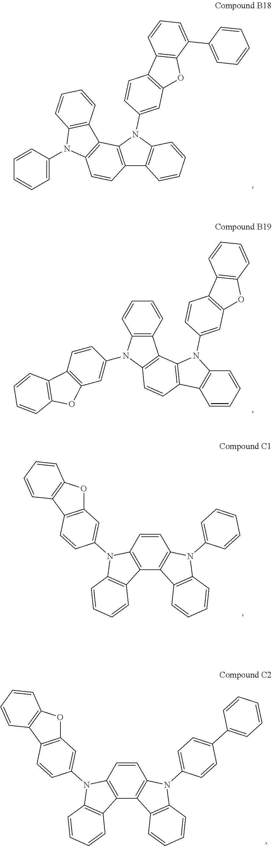
[0140] Compound B19
##STR00122##
[0141] A solution of 5,12-dihydroindolo[3,2-.alpha.]carbazole (2.86 g, 11.16 mmol), 3-bromodibenzo[b,d]furan (6.20 g, 25.1 mmol), Pd.sub.2(dba).sub.3 (0.20 g, 0.22 mmol), SPhos (0.18 g, 0.45 mmol) and tert-BuONa (4.29 g, 44.6 mmol) xylene (120 ml) was refluxed under nitrogen for 16 h. The solvent was evaporated and the residue was purified by column chromatography on silica gel with heptane/dichloromethane (1/1, v/v) as eluent and recrystallized from the same solvent to yield Compound B19 (4.5 g, 69%) as white crystals.
[0142] Compound C28
##STR00123##
[0143] The procedure for the synthesis of Compound B19 was followed to synthesize Compound C28 from 5,8-dihydroindolo[2,3-c]carbazole and 3-bromodibenzo[b,d]furan. Compound C28 was prepared as a white solid in a yield of 71%.
[0144] Compound D9
##STR00124##
[0145] The procedure for the synthesis of Compound A1 was followed to synthesize Compound D9 from 5-phenyl-5,7-dihydroindolo[2,3-b]carbazole and 3-bromodibenzo[b,d]furan as a white solid in a yield of 78%.
[0146] Compound E2
##STR00125##
[0147] The procedure for the synthesis of Compound A1 was followed to synthesize Compound E2 from 3-bromodibenzo[b,d]furan and 6-(9H-carbazol-3-yl)indolo[3,2,1-jk]carbazole. Compound E2 was prepared as a white solid in a yield of 60%.
[0148] Compound E4
##STR00126##
[0149] The procedure for the synthesis of Compound A1 was followed to synthesize Compound E4 from 2-(9H-car2bazol-3-yl)indolo[3,2,1-jk]carbazole and 3-bromodibenzo[b,d]furan. Compound E4 was prepared as a white solid in a yield of 81%.
Application in OLED.
[0150] All devices were fabricated by high vacuum (.about.10.sup.-7 Torr) thermal evaporation. The anode electrode was 80 nm of indium tin oxide (ITO). The cathode electrode consisted of 1 nm of LiQ followed by 100 nm of Al. All devices were encapsulated with a glass lid sealed with an epoxy resin in a nitrogen glove box (<1 ppm of H.sub.2O and O.sub.2) immediately after fabrication, and a moisture getter was incorporated inside the package.
DEVICE EXAMPLES
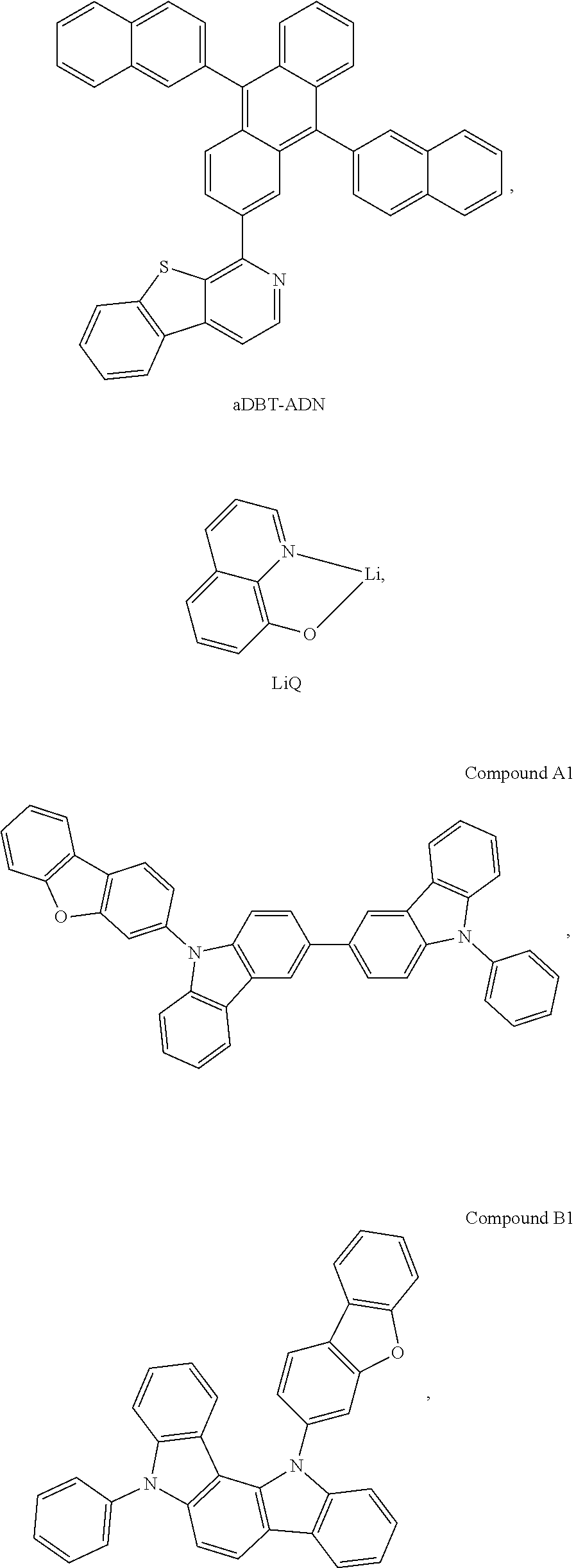
[0151] A set of device examples have organic stacks consisting of, sequentially from the ITO surface, 10 nm of LG101 (from LG Chem) as the hole injection layer (HIL), 45 nm of PPh-TPD as the hole-transport layer (HTL), 40 nm of emissive layer (EML), 5 nm of EH-1 as the hole-blocking layer (HBL), followed by 30 nm of aDBT-ADN with 35 wt % LiQ as the electron-transport layer (ETL). The EML has three components: 50 wt % of the EML being the invented compounds (Compound A1, Compound B1 or Compound B12) or comparative compound (CC-1 or CC-2) as the first host; 40 wt.% of EML being compound EH-1 as the second host; and 10 wt % of the EML being compound GD as the emitter. The chemical structures of the compounds used are shown below.
##STR00127## ##STR00128## ##STR00129##
Provided in Table D1 below is a summary of the device data recorded at 1000 nits for device examples. The relative lifetime LT97 (in arbitrary unit, A.U.), defined as the time it takes for a device to decay to 97% of its original luminescence under a constant operation current density that provides an initial luminescence of 1000 nits, is calculated from the measured value recorded at 40 mA/cm.sup.2, assuming an acceleration factor of 1.8, and is normalized to that of Device C-2.
TABLE-US-00001 TABLE D1 EML Emission LT97 Device ID 1.sup.st Host 2.sup.nd Host Dopant Color [A.U.] Device 1 Compound A1 EH-1 GD Green 364 Device C-1 CC-1 EH-1 GD Green 123 Device 2 Compound B1 EH-1 GD Green 267 Device 3 Compound B12 EH-1 GD Green 188 Device C-2 CC-2 EH-1 GD Green 100
[0152] The data in Table D1 shows that the devices using the inventive compounds as the hosts achieves longer lifetime than the devices using the comparative compounds as the host. A comparison between Compound B1, Compound B12 and CC-2 shows that a dibenzofuran moiety is necessary to improve device lifetime. It is noted that the only difference between Compound A1 and CC-1 is that Compound A1 has a dibenzofuran moiety while CC-1 has a dibenzothiophene moiety. Conventional wisdom is that hosts containing dibenzothiophene are more stable than those containing dibenzofuran. The superior performance of Compound A1 over CC-1 is unexpected.
[0153] It is understood that the various embodiments described herein are by way of example only, and are not intended to limit the scope of the invention. For example, many of the materials and structures described herein may be substituted with other materials and structures without deviating from the spirit of the invention. The present invention as claimed may therefore include variations from the particular examples and preferred embodiments described herein, as will be apparent to one of skill in the art. It is understood that various theories as to why the invention works are not intended to be limiting.
* * * * *


D00000

D00001

D00002

XML
uspto.report is an independent third-party trademark research tool that is not affiliated, endorsed, or sponsored by the United States Patent and Trademark Office (USPTO) or any other governmental organization. The information provided by uspto.report is based on publicly available data at the time of writing and is intended for informational purposes only.
While we strive to provide accurate and up-to-date information, we do not guarantee the accuracy, completeness, reliability, or suitability of the information displayed on this site. The use of this site is at your own risk. Any reliance you place on such information is therefore strictly at your own risk.
All official trademark data, including owner information, should be verified by visiting the official USPTO website at www.uspto.gov. This site is not intended to replace professional legal advice and should not be used as a substitute for consulting with a legal professional who is knowledgeable about trademark law.