Flexible Thin-film Transistor Using Two-dimensional Semiconductor Material
CHOI; Sung-Yool ; et al.
U.S. patent application number 16/715021 was filed with the patent office on 2020-06-18 for flexible thin-film transistor using two-dimensional semiconductor material. This patent application is currently assigned to Korea Advanced Institute of Science and Technology. The applicant listed for this patent is Korea Advanced Institute of Science and Technology. Invention is credited to Sung-Yool CHOI, Young jun WOO.
| Application Number | 20200194595 16/715021 |
| Document ID | / |
| Family ID | 71072947 |
| Filed Date | 2020-06-18 |


| United States Patent Application | 20200194595 |
| Kind Code | A1 |
| CHOI; Sung-Yool ; et al. | June 18, 2020 |
FLEXIBLE THIN-FILM TRANSISTOR USING TWO-DIMENSIONAL SEMICONDUCTOR MATERIAL
Abstract
Provided is a flexible thin-film transistor using a two-dimensional semiconductor material, which includes: a flexible substrate; a channel formed on the flexible substrate and formed of a two-dimensional semiconductor material; a gate insulator and a gate electrode stacked sequentially on the channel; and source and drain electrodes formed on the channel as being spaced apart from the gate electrode.
| Inventors: | CHOI; Sung-Yool; (Daejeon, KR) ; WOO; Young jun; (Daejeon, KR) | ||||||||||
| Applicant: |
|
||||||||||
|---|---|---|---|---|---|---|---|---|---|---|---|
| Assignee: | Korea Advanced Institute of Science
and Technology Daejeon KR |
||||||||||
| Family ID: | 71072947 | ||||||||||
| Appl. No.: | 16/715021 | ||||||||||
| Filed: | December 16, 2019 |
| Current U.S. Class: | 1/1 |
| Current CPC Class: | H01L 29/78681 20130101; H01L 29/66742 20130101; H01L 29/778 20130101; H01L 29/24 20130101; H01L 29/78603 20130101; H01L 29/517 20130101; H01L 27/1218 20130101; H01L 21/0228 20130101; H01L 27/1225 20130101 |
| International Class: | H01L 29/786 20060101 H01L029/786; H01L 29/66 20060101 H01L029/66; H01L 21/02 20060101 H01L021/02 |
Foreign Application Data
| Date | Code | Application Number |
|---|---|---|
| Dec 14, 2018 | KR | 10-2018-0162133 |
Claims
1. A flexible thin-film transistor using a two-dimensional semiconductor material, which comprises: a flexible substrate; a channel formed on the flexible substrate and formed of a two-dimensional semiconductor material; a gate insulator and a gate electrode stacked sequentially on the channel; and source and drain electrodes formed on the channel as being spaced apart from the gate electrode wherein the flexible substrate has a roughness of 1.5 nm or smaller.
2. The flexible thin-film transistor according to claim 1, wherein the two-dimensional semiconductor material comprises a transition metal dichalcogenide compound.
3. The flexible thin-film transistor according to claim 2, wherein the two-dimensional semiconductor material comprising the transition metal dichalcogenide compound is formed on another substrate through chemical vapor deposition and then transferred to the flexible substrate.
4. A flexible thin-film transistor array comprising at least two flexible thin-film transistors according to claim 1.
5. A method for preparing a flexible thin-film transistor, which comprises: a step of sequentially forming a gate electrode and a gate insulator on a flexible substrate; a step of forming a channel by transferring a two-dimensional semiconductor material thin film formed on another substrate through chemical vapor deposition to the gate insulator; and a step of forming source and drain electrodes on the two-dimensional semiconductor material thin film.
6. The method for preparing a flexible thin-film transistor according to claim 5, wherein the two-dimensional semiconductor material comprises a transition metal dichalcogenide compound.
7. The method for preparing a flexible thin-film transistor according to claim 6, wherein the two-dimensional semiconductor material comprises any one selected from a group consisting of molybdenum disulfide (MoS.sub.2), molybdenum diselenide (MoSe.sub.2), molybdenum ditelluride (MoTe.sub.2), tungsten disulfide (WS.sub.2), tungsten diselenide (WSe.sub.2) and tungsten ditelluride (WTe.sub.2).
8. The method for preparing a flexible thin-film transistor according to claim 5, wherein the flexible substrate has a roughness of 1.5 nm or smaller.
Description
CROSS-REFERENCE TO RELATED APPLICATION
[0001] This application claims the benefit under 35 USC .sctn. 119(a) of Korean Patent Application No. 10-2018-0162133 filed on Dec. 14, 2018, in the Korean Intellectual Property Office, the entire disclosure of which is incorporated herein by reference for all purposes.
TECHNICAL FIELD
[0002] The present disclosure relates to a flexible thin-film transistor using a two-dimensional semiconductor material, more particularly to a flexible thin-film transistor array that can be used as a display driving circuit, which is fabricated on a flexible substrate through chemical vapor deposition and exhibits flexibility and transistor driving characteristics at the same time.
BACKGROUND ART
[0003] A two-dimensional semiconductor material has drawn a lot of attentions due to superior electrical, mechanical and optical properties. In general, the two-dimensional semiconductor material refers to a layered semiconductor material which has a strong covalent bond in the horizontal direction and a weak van der Waals bond in the vertical direction. Although various methods of utilizing two-dimensional semiconductor materials, e.g., transition metal dichalcogenide compounds, as devices are presented, application as effective devices has not been disclosed yet.
[0004] For example, Korean Patent Publication No. 10-2017-0098053 discloses a thin-film transistor wherein a transition metal dichalcogenide compound is used on a substrate as a channel material. Although it is advantageous in terms of flexibility and miniaturization when compared with display driving thin-film transistors based on amorphous silicon, low-temperature polycrystalline silicon or metal oxides, it is limited mostly to mechanically exfoliated samples or small-area thin-film-based single devices due to the limitation of growth technology.
DISCLOSURE
Technical Problem
[0005] The present disclosure is directed to providing a flexible thin-film transistor array which exhibits superior flexibility and device driving characteristics, and a method for preparing the same.
Technical Solution
[0006] The present disclosure provides a flexible thin-film transistor using a two-dimensional semiconductor material, which includes: a flexible substrate; a channel formed on the flexible substrate and formed of a two-dimensional semiconductor material; a gate insulator and a gate electrode stacked sequentially on the channel; and source and drain electrodes formed on the channel as being spaced apart from the gate electrode.
[0007] In an exemplary embodiment of the present disclosure, the two-dimensional semiconductor material includes a transition metal dichalcogenide compound.
[0008] In an exemplary embodiment of the present disclosure, the two-dimensional semiconductor material including the transition metal dichalcogenide compound is formed on another substrate through chemical vapor deposition and then transferred to the flexible substrate.
[0009] In an exemplary embodiment of the present disclosure, the flexible substrate has a roughness of 1.5 nm or smaller.
[0010] The present disclosure also provides a flexible thin-film transistor array including at least two flexible thin-film transistors described above.
[0011] The present disclosure provides a method for preparing a flexible thin-film transistor, which includes: a step of sequentially forming a gate electrode and a gate insulator on a flexible substrate; a step of forming a channel by transferring a two-dimensional semiconductor material thin film formed on another substrate through chemical vapor deposition to the gate insulator; and a step of forming source and drain electrodes on the two-dimensional semiconductor material thin film.
[0012] In an exemplary embodiment of the present disclosure, the two-dimensional semiconductor material includes a transition metal dichalcogenide compound.
[0013] In an exemplary embodiment of the present disclosure, the two-dimensional semiconductor material includes any one selected from a group consisting of molybdenum disulfide (MoS.sub.2), molybdenum diselenide (MoSe.sub.2), molybdenum ditelluride (MoTe.sub.2), tungsten disulfide (WS.sub.2), tungsten diselenide (WSe.sub.2) and tungsten ditelluride (WTe.sub.2).
[0014] In an exemplary embodiment of the present disclosure, the flexible substrate has a roughness of 1.5 nm or smaller.
Advantageous Effects
[0015] According to the present disclosure, a flexible thin-film transistor exhibiting superior flexibility and device driving characteristics at the same time can be prepared by transferring a two-dimensional semiconductor material with a thickness controlled to 50 nm or smaller onto a flatness-controlled flexible substrate through chemical vapor deposition. The flexible thin-film transistor can be utilized as a driving circuit of a display.
BRIEF DESCRIPTION OF DRAWINGS
[0016] The patent or application file contains a least one drawing executed in color. Copies of this patent or patent application publication with color drawing(s) will be provided by the Office upon request and payment of the necessary fee.
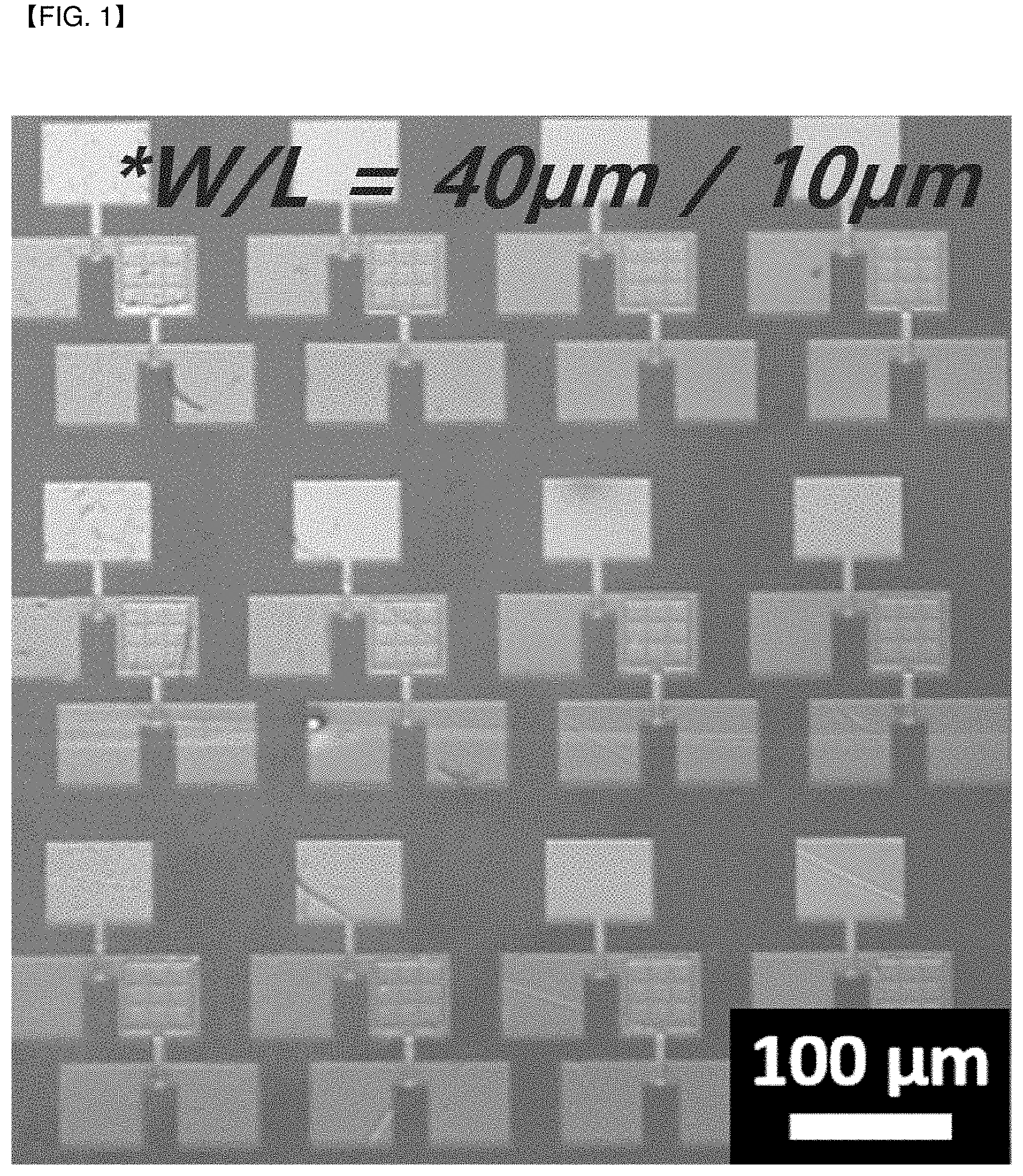
[0017] FIG. 1 shows a photographic image of a thin-film transistor completed according to an exemplary embodiment of the present disclosure.
[0018] FIG. 2A to 2C show results of AFM analysis for validating the effectiveness of a flattening process.
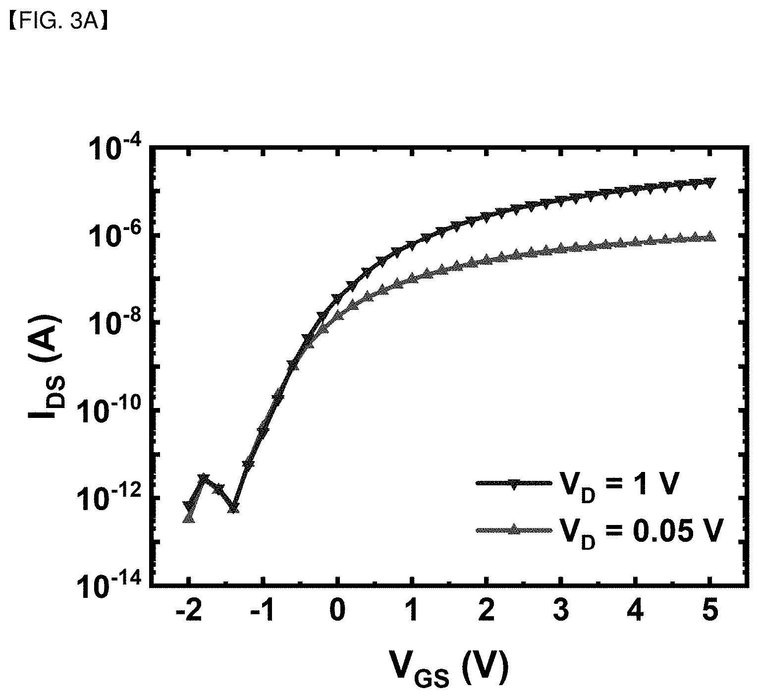
[0019] FIG. 3A and 3B show results of analyzing single device operating characteristic data.
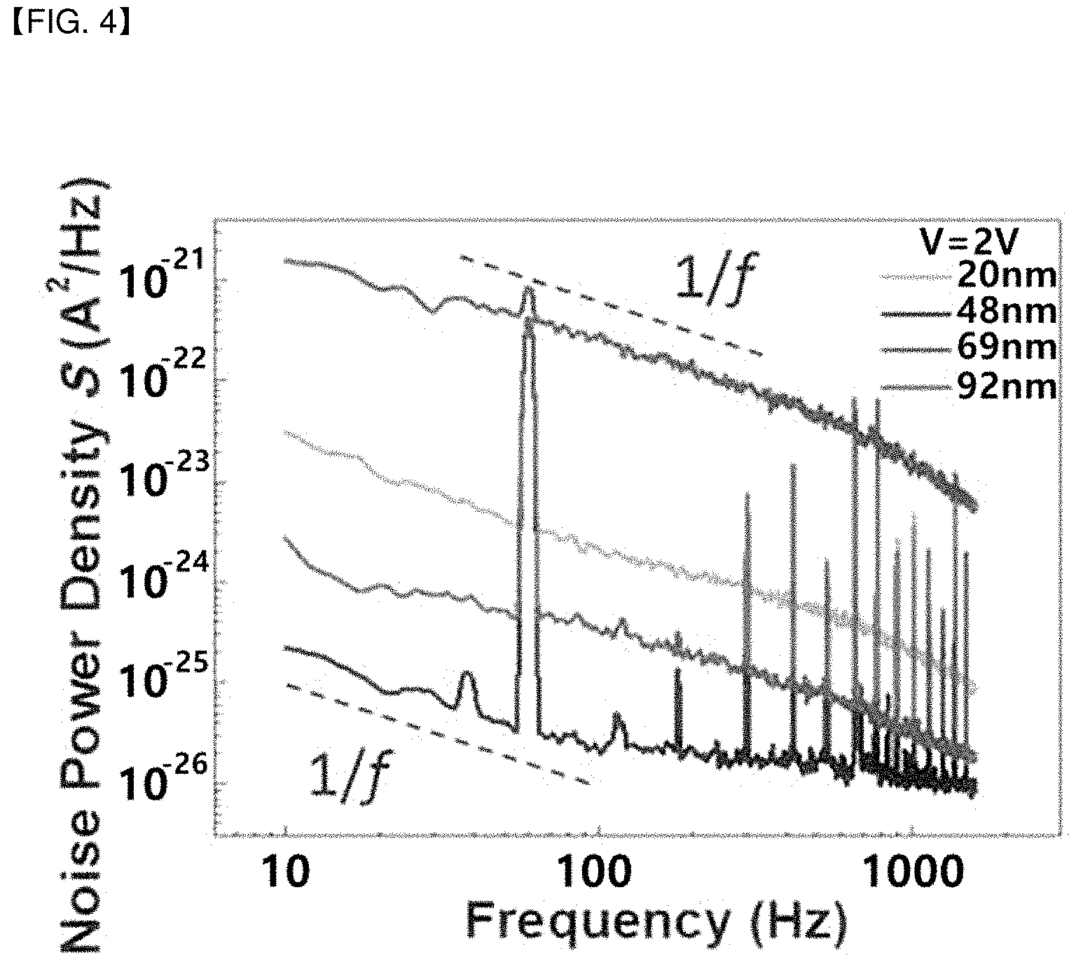
[0020] FIG. 4 shows a result of analyzing display pixel driving circuit characteristic data.
BEST MODE FOR CARRYING OUT INVENTION
[0021] In the present disclosure, a flexible thin-film transistor is prepared by transferring a two-dimensional semiconductor material with a thickness controlled to 50 nm or smaller onto a flatness-controlled flexible substrate through chemical vapor deposition. In an exemplary embodiment of the present disclosure, the transition metal dichalcogenide compound molybdenum disulfide (MoS.sub.2) may be used as the two-dimensional semiconductor material. Any one selected from a group consisting of molybdenum diselenide (MoSe.sub.2), molybdenum ditelluride (MoTe.sub.2), tungsten disulfide (WS.sub.2), tungsten diselenide (WSe.sub.2) and tungsten ditelluride (WTe.sub.2) may also be used.
EXAMPLE 1
[0022] Because it is difficult to use a commercially available polyimide film as a substrate for a flexible electronic device due to surface roughness, SU-8, which is an epoxy resin-based negative photoresist was coated and then treated with UV to reduce surface roughness.
[0023] Cr, Au and Pd layers were formed on the substrate through photolithography, thermal evaporation and lift-off processes for use as a gate of a thin-film transistor.
[0024] A gate insulator was formed on the gate layer by depositing an Al.sub.2O.sub.3 film through ALD (atomic layer deposition). Then, an active layer (channel) of a thin-film transistor was formed through wet transfer of a molybdenum disulfide thin film formed through chemical vapor deposition onto polystyrene as a supporting layer. After the transfer, the polystyrene supporting layer was dissolved using toluene.
[0025] Then, after forming an active layer pattern through photolithography, source and drain electrodes were formed thereon by depositing Ti and Au through photolithography, thermal evaporation and lift-off processes. Finally, a protective film was deposited by ALD to protect the thin-film transistor.
[0026] FIG. 1 shows a photographic image of the thin-film transistor completed according to an exemplary embodiment of the present disclosure.
TEST EXAMPLE
[0027] First, AFM analysis was conducted to validate the effectiveness of the flattening process using the SU-8 epoxy resin-based negative photoresist.
[0028] FIG. 2A to 2C show results of the AFM analysis for validating the effectiveness of the flattening process.
[0029] FIG. 2A to 2C show surface roughness: (2A) before the SU-8 coating; (2B) after coating to a thickness of 0.5 .mu.m; and (2C) after coating to a thickness of 2 .mu.m. Whereas (2A) shows a roughness of 50 nm or larger, (2B) and (2C) show a roughness of 1.5 nm or smaller. Considering that each layer of the thin-film transistor has a thickness of tens of nanometers, it can be seen that (2B) and (2C) will provide improved stability and yield during deposition or other processes.
[0030] FIG. 3 show results of analyzing single device operating characteristic data.
[0031] Referring to FIG. 3A, it can be seen that, as a result of measuring the magnitude of source-drain current depending on gate voltage in order to check the basic operation of the thin-film transistor, the ON current is suitable for driving OLED pixels, etc. and the ON-OFF current ratio is suitable for control of pixel lightness.
[0032] FIG. 3B shows a result of conducting the same measurement while bending the substrate of the transistor. It can be seen that the operation of the transistor is maintained even at a curvature of about 3.5 mm.
[0033] FIG. 4 shows a result of analyzing display pixel driving circuit characteristic data.
[0034] Referring to FIG. 4, the most basic OLED pixel driving circuit was realized using two transistors fabricated according to an exemplary embodiment of the present disclosure as one group, and its electrical properties were analyzed. FIG. 4 shows the result for (a) unbent state and (b) bent state with a curvature of 3.5 mm. It can be seen that the magnitude of current is controlled well depending on the applied voltage for both cases.
* * * * *
D00000
D00001
D00002
D00003
D00004
D00005
D00006
D00007
XML
uspto.report is an independent third-party trademark research tool that is not affiliated, endorsed, or sponsored by the United States Patent and Trademark Office (USPTO) or any other governmental organization. The information provided by uspto.report is based on publicly available data at the time of writing and is intended for informational purposes only.
While we strive to provide accurate and up-to-date information, we do not guarantee the accuracy, completeness, reliability, or suitability of the information displayed on this site. The use of this site is at your own risk. Any reliance you place on such information is therefore strictly at your own risk.
All official trademark data, including owner information, should be verified by visiting the official USPTO website at www.uspto.gov. This site is not intended to replace professional legal advice and should not be used as a substitute for consulting with a legal professional who is knowledgeable about trademark law.