Method Of Forming A Device Structure Using Selective Deposition Of Gallium Nitride And System For Same
Banerjee; Sourish ; et al.
U.S. patent application number 16/712707 was filed with the patent office on 2020-06-18 for method of forming a device structure using selective deposition of gallium nitride and system for same. The applicant listed for this patent is ASM IP Holding B.V. UNIVERSITY TWENTE NEDERLANDSE ORGANISATIE VOOR WETENSCHAPPELIJK ONDERZOEK. Invention is credited to Antonius Aarnink, Sourish Banerjee, Alexey Kovalgin.
| Application Number | 20200194253 16/712707 |
| Document ID | / |
| Family ID | 71072881 |
| Filed Date | 2020-06-18 |


| United States Patent Application | 20200194253 |
| Kind Code | A1 |
| Banerjee; Sourish ; et al. | June 18, 2020 |
METHOD OF FORMING A DEVICE STRUCTURE USING SELECTIVE DEPOSITION OF GALLIUM NITRIDE AND SYSTEM FOR SAME
Abstract
A method of forming a device structure including a selectively-deposited gallium nitride layer is disclosed.
| Inventors: | Banerjee; Sourish; (Enschede, NL) ; Aarnink; Antonius; (Enschede, NL) ; Kovalgin; Alexey; (Enschede, NL) | ||||||||||
| Applicant: |
|
||||||||||
|---|---|---|---|---|---|---|---|---|---|---|---|
| Family ID: | 71072881 | ||||||||||
| Appl. No.: | 16/712707 | ||||||||||
| Filed: | December 12, 2019 |
Related U.S. Patent Documents
| Application Number | Filing Date | Patent Number | ||
|---|---|---|---|---|
| 62779684 | Dec 14, 2018 | |||
| Current U.S. Class: | 1/1 |
| Current CPC Class: | C23C 16/45527 20130101; H01L 21/02458 20130101; C23C 16/56 20130101; H01L 21/0254 20130101; H01L 21/30612 20130101; H01L 21/02502 20130101; H01L 21/02636 20130101; C23C 16/303 20130101; H01L 21/0262 20130101 |
| International Class: | H01L 21/02 20060101 H01L021/02; H01L 21/306 20060101 H01L021/306; C23C 16/56 20060101 C23C016/56; C23C 16/30 20060101 C23C016/30; C23C 16/455 20060101 C23C016/455 |
Claims
1. A method of forming a device structure, the method comprising the steps of: providing a substrate, comprising a surface, within a reaction chamber, the surface comprising a first portion comprising one or more of aluminum nitride and gallium nitride and a second portion comprising another material; and using a thermal cyclic deposition process, selectively depositing gallium nitride on the first portion relative to the second portion.
2. The method of claim 1, wherein the second portion comprises silicon.
3. The method of claim 2, wherein the second portion comprises hydrogen-terminated silicon.
4. The method of claim 1, wherein the second portion comprises one or more of an oxide, a nitride, and an oxynitride.
5. The method of claim 1, wherein the second portion comprises a hydroxyl-terminated oxide.
6. The method of claim 1, wherein the step of selectively depositing gallium nitride and the step of forming the first portion comprising one or more of aluminum nitride and gallium nitride are performed ex situ.
7. The method of claim 1, further comprising a step of exposing the first portion to a reducing agent prior to the step of selectively depositing gallium nitride.
8. The method of claim 7, wherein the step of exposing the first portion to a reducing agent and the step of selectively depositing gallium nitride are performed in the same reaction chamber without a vacuum break.
9. The method of claim 7, wherein the reducing agent comprises one or more of hydrogen, ammonia, and hydrazine, or radicals formed from a source gas comprising one or more of hydrogen, ammonia, and hydrazine.
10. The method of claim 1, wherein the one or more of aluminum nitride and gallium nitride is formed by depositing a layer comprising the one or more of aluminum nitride and gallium nitride using a method selected from the list consisting of chemical vapor deposition, cyclic deposition, atomic layer deposition, molecular beam epitaxy, and physical vapor deposition.
11. The method of claim 10, wherein the method of forming a device structure further comprises patterning the layer comprising the one or more of aluminum nitride and gallium nitride to form features comprising the one or more of aluminum nitride and gallium nitride.
12. The method of claim 11, further comprising a step of etching a surface of the features.
13. The method of claim 11, further comprising a step of removing an oxide from a surface of the features.
14. The method of claim 1, wherein the first portion comprises aluminum nitride, wherein the aluminum nitride is deposited using chemical vapor deposition or atomic layer deposition, and wherein an aluminum precursor for forming the aluminum nitride is selected from the group consisting of TMA, TEA, and AlCl.sub.3.
15. The method of claim 1, wherein the first portion comprises gallium nitride, wherein the gallium nitride is deposited using chemical vapor deposition or atomic layer deposition, and wherein a gallium precursor for forming the gallium nitride is selected from the group consisting of TMG, TEG, GaCl.sub.3 GaBr.sub.3 and GaI.sub.3.
16. The method of claim 14, further comprising a step of providing a nitrogen precursor, wherein the nitrogen precursor is selected from the group consisting of ammonia (NH.sub.3) and hydrazine (N.sub.2H.sub.4) and/or radicals remotely created from a precursor selected from the group of Nitrogen (N.sub.2), ammonia (NH.sub.3) and hydrazine (N.sub.2H.sub.4).
17. The method of claim 1, wherein during the step of using a thermal cyclic deposition process, the selectivity is greater than 80%.
18. A method of forming a device structure, the method comprising the steps of: providing a substrate comprising a surface, the surface comprising a first portion comprising one or more of aluminum nitride and gallium nitride and a second portion comprising silicon nitride; and using a thermal cyclic deposition process, selectively depositing gallium nitride on the first portion relative to the second portion.
19. The method according to claim 1, wherein, during the step of selectively depositing gallium nitride, a pressure within the reaction chamber is between about 1 and about 100 mbar.
20. The method according to claim 1, wherein, during the step of selectively depositing gallium nitride, a pressure within the reaction chamber is between about 5 and about 15 mbar.
21. The method according to claim 1, wherein, during the step of selectively depositing gallium nitride, a temperature within the reaction chamber is between about 375.degree. C. and about 425.degree. C.
22. The method according to claim 1, wherein, during the step of selectively depositing gallium nitride, the selectivity is greater than 80%.
23. A structure formed according to the method of claim 1.
24. A system for performing the method of claim 1.
Description
CROSS-REFERENCE TO RELATED APPLICATIONS
[0001] This application is a nonprovisional application of, and claims priority to and the benefit of, U.S. Provisional Patent Application Ser. No. 62/779,684, filed Dec. 14, 2018 and entitled METHOD OF FORMING A DEVICE STRUCTURE USING SELECTIVE DEPOSITION OF GALLIUM NITRIDE AND SYSTEM FOR SAME, which is hereby incorporated by reference.
FIELD OF THE DISCLOSURE
[0002] The present disclosure generally relates to thin-film deposition methods, to structures formed using the methods, and to systems for performing the methods. More particularly, the disclosure relates to methods of selectively depositing gallium nitride to form device structures and to related structures and systems.
BACKGROUND OF THE DISCLOSURE
[0003] Gallium nitride (GaN) is a direct bandgap material that exhibits relatively high electron mobility and a relatively wide bandgap, compared to silicon. Accordingly, gallium nitride has gained increasing attention for use in a variety of devices, including optoelectrical devices, such as photovoltaic devices; light-emitting devices, such as lasers and light-emitting diodes; high power, high frequency transistors, such as high-electron-mobility transistors (HEMT), metal-oxide-semiconductor field-effect transistors (MOSFET) and metal-semiconductor field-effect transistors (MESFET); resonators; and the like.
[0004] Although gallium nitride has many desirable properties, gallium nitride substrates are relatively expensive, compared to silicon substrates. Accordingly, methods of forming devices including gallium nitride typically include steps of depositing a layer of gallium nitride overlying a silicon substrate and subsequently patterning the gallium nitride layer using lithography and etch techniques. Such processes allow monolithic integration of gallium nitride devices with silicon-based devices. While such processes work well for a variety of applications, the processes may be relatively time consuming and expensive, and may not offer the precision desired for other applications. Accordingly, improved methods for forming device structures including gallium nitride are desired.
SUMMARY OF THE DISCLOSURE
[0005] Various embodiments of the present disclosure relate to methods of forming a device structure that includes selective deposition of gallium nitride on one material relative to another material. While the ways in which various embodiments of the present disclosure address drawbacks of prior methods are discussed in more detail below, in general, various embodiments of the disclosure allow for the formation of device structures including (e.g., patterned) layers of gallium nitride using fewer steps and/or allow the formation of device structures having relatively small gallium nitride features.
[0006] In accordance with exemplary embodiments of the disclosure, a method of forming a device structure includes providing a substrate, including a surface, within a reaction chamber, the surface comprising a first portion comprising one or more of aluminum nitride and gallium nitride (or other boron group (Group III) nitrides, such as BN, InN, or transition metal(s)) and a second portion comprising another material, and using a thermal cyclic deposition process (e.g., an atomic layer deposition process), selectively depositing gallium nitride on the first portion relative to the second portion. In accordance with various aspects of these embodiments, the second portion can include silicon. The silicon can be hydrogen terminated. In accordance with additional aspects, the second portion can include one or more of an oxide, a nitride, and an oxynitride. The second portion (e.g., oxide, nitride, or oxynitride) can be hydroxyl terminated. Exemplary methods can further include a step of exposing the first portion to a reducing and/or nitriding agent, such as one or more of hydrogen, ammonia, and hydrazine, and/or radical species formed from a source gas comprising one or more of hydrogen, ammonia, and hydrazine, prior to the step of selectively depositing gallium nitride. Exemplary methods can additionally or alternatively include forming features comprising the one or more of aluminum nitride and gallium nitride (or other Group III nitride or transition metal(s)). The surface of the features can be etched to, for example, remove a native oxide or other debris from the surface of the features.
[0007] In accordance with additional embodiments of the disclosure, a method of forming a device structure includes the steps of: providing a substrate comprising a surface, the surface comprising a first portion comprising one or more of aluminum nitride and gallium nitride or other Group III nitride or transition metal(s) and a second portion comprising silicon nitride, and using a thermal cyclic deposition process (e.g., an atomic layer deposition process), selectively depositing gallium nitride on the first portion relative to the second portion.
[0008] In accordance with yet further exemplary embodiments of the disclosure, a device structure is formed using a method as described herein.
[0009] And, in accordance with yet additional embodiments of the disclosure, a system for performing a method as described herein is provided.
[0010] For purposes of summarizing the invention and the advantages achieved over the prior art, certain objects and advantages of the invention have been described herein above. Of course, it is to be understood that not necessarily all such objects or advantages may be achieved in accordance with any particular embodiment of the invention. Thus, for example, those skilled in the art will recognize that the invention may be embodied or carried out in a manner that achieves or optimizes one advantage or group of advantages as taught or suggested herein without necessarily achieving other objects or advantages as may be taught or suggested herein.
[0011] All of these embodiments are intended to be within the scope of the invention herein disclosed. These and other embodiments will become readily apparent to those skilled in the art from the following detailed description of certain embodiments having reference to the attached figures, the invention not being limited to any particular embodiment(s) disclosed.
BRIEF DESCRIPTION OF THE DRAWING FIGURES
[0012] A more complete understanding of exemplary embodiments of the present disclosure can be derived by referring to the detailed description and claims when considered in connection with the following illustrative figures.
[0013] FIG. 1 illustrates a method in accordance with exemplary embodiments of the disclosure.
[0014] FIG. 2 illustrates a step of the method illustrated in FIG. 1 in more detail.
[0015] FIG. 3 illustrates a device structure in accordance with exemplary embodiments of the disclosure.
[0016] FIG. 4 illustrates a system for performing methods in accordance with embodiments of the disclosure.
[0017] It will be appreciated that elements in the figures are illustrated for simplicity and clarity and have not necessarily been drawn to scale. For example, the dimensions of some of the elements in the figures may be exaggerated relative to other elements to help to improve the understanding of illustrated embodiments of the present disclosure.
DETAILED DESCRIPTION OF EXEMPLARY EMBODIMENTS OF THE DISCLOSURE
[0018] The description of exemplary embodiments provided below is merely exemplary and is intended for purposes of illustration only; the following description is not intended to limit the scope of the disclosure or the claims. Moreover, recitation of multiple embodiments having stated features is not intended to exclude other embodiments having additional features or other embodiments incorporating different combinations of the stated features. Further, the illustrations presented herein are not meant to be actual views of any particular material, structure, or device, but are merely idealized representations that are used to describe embodiments of the disclosure.
[0019] The present disclosure generally relates to methods of forming structures and to structures formed using the methods. The methods and structures described herein can be used to form a variety of devices, such as, for example, devices that include monocrystalline and/or polycrystalline gallium nitride layers.
[0020] As used herein, a layer including gallium nitride can comprise, consist essentially of, or consist of gallium nitride material (with or without a dopant). Films consisting of gallium nitride (with or without a dopant) can include an acceptable amount of impurities, such as carbon that may originate from one or more precursors used to deposit the gallium nitride layers.
[0021] Similarly, a surface or portion including aluminum nitride can comprise, consist essentially of, or consist of aluminum nitride material. Films consisting of aluminum nitride can include an acceptable amount of impurities, such as carbon that may originate from one or more precursors used to deposit the aluminum nitride layers.
[0022] As used herein, the term substrate may refer to any underlying material or materials upon which material can be deposited. Exemplary substrates can be used to form a device, a circuit, or a structure. By way of examples, a substrate can be or include semiconductor material, such as but not limited to, silicon (Si), germanium (Ge), germanium tin (GeSn), silicon germanium (SiGe), silicon germanium tin (SiGeSn), silicon carbide (SiC), or a group III-V semiconductor material, such as, for example, gallium arsenide (GaAs), gallium phosphide (GaP), or gallium nitride (GaN). In some embodiments of the disclosure, the substrate may include an engineered substrate wherein a surface semiconductor layer is disposed over a bulk support with an intervening buried oxide (BOX) disposed therebetween. The substrate can be patterned. Patterned substrates may comprise substrates that may include semiconductor device structures formed into or onto a surface of the substrate; for example, a patterned substrate may comprise partially fabricated semiconductor device structures, such as, for example, transistors and/or memory elements. In some embodiments, the substrate may contain monocrystalline surfaces and/or one or more secondary surfaces that may comprise a non-monocrystalline surface, such as a polycrystalline surface and/or an amorphous surface. Monocrystalline surfaces may comprise, for example, one or more of silicon (Si), silicon germanium (SiGe), germanium tin (GeSn), or germanium (Ge). Polycrystalline or amorphous surfaces may include dielectric materials, such as oxides, oxynitrides or nitrides, such as, for example, silicon oxides and silicon nitrides.
[0023] As used herein, the term "cyclic deposition" may refer to the sequential introduction of reactants into a reaction chamber to deposit a film over a substrate and includes deposition techniques such as atomic layer deposition and cyclical chemical vapor deposition.
[0024] As used herein, the term "cyclical chemical vapor deposition" may refer to any process wherein a substrate is sequentially exposed to two or more volatile reactants, which react and/or decompose on a substrate to produce a desired material.
[0025] As used herein, the term atomic layer deposition (ALD) may refer to a vapor deposition process in which deposition cycles, for example, a plurality of consecutive deposition cycles, are conducted in a reaction chamber. Typically, during each cycle, a first precursor is chemisorbed to a deposition surface (e.g., a substrate surface or a previously deposited underlying material, such as material from a previous ALD cycle), forming a monolayer or sub-monolayer that does not readily react with additional precursor (i.e., a self-limiting reaction). Thereafter, a reactant (e.g., another precursor or reaction gas) may subsequently be introduced into the process chamber for use in converting the chemisorbed precursor to the desired material on the deposition surface. Typically, this reactant is capable of further reaction with the precursor. Further, purging steps may also be utilized during each cycle to remove excess precursor from the process chamber and/or remove excess reactant and/or reaction byproducts from the process chamber after conversion of the chemisorbed precursor. The term atomic layer deposition, as used herein, is also meant to include processes designated by related terms, such as chemical vapor atomic layer deposition, atomic layer epitaxy (ALE), molecular beam epitaxy (MBE), gas source MBE, or organometallic MBE, and chemical beam epitaxy when performed with alternating pulses of precursor composition(s), reactive gas, and purge (e.g., inert carrier) gas.
[0026] As used herein, the terms layer, film and thin film may refer to any continuous or non-continuous structures and material formed by the methods disclosed herein. For example, layer, film and thin film could include 2D materials, nanolaminates, nanorods, nanotubes, or nanoparticles, or even partial or full molecular layers, or partial or full atomic layers or clusters of atoms and/or molecules. Layer, film, and thin film may comprise material or a layer with pinholes, but still be at least partially continuous.
[0027] As used herein, the term "incubation period" may refer to the number of cyclical deposition cycles in the initial stages of a cyclical deposition in which no discernable deposition is observed.
[0028] A selective deposition process as described herein can involve a greater amount of material remaining on a first surface or portion relative to a second surface or portion. For example, a selective process may result in a greater amount of gallium nitride material remaining in a first area relative to any gallium nitride remaining in a second area. In some embodiments of the disclosure, a selectivity of a process can be expressed as a ratio of material remaining on the first surface relative to the amount of material formed on the first and second surfaces combined. For example, if 10 nm of gallium nitride material remains in the first area and 1 nm gallium nitride material remains in the second area, the selective deposition process will be considered to have 90% selectivity. In some embodiments, the selectivity of the methods disclosed herein may be greater than 80%, greater than 90%, greater than 95%, greater than 99.5%, greater than 98%, greater than 99%, or even about 100%.
[0029] Turning now to the figures, FIG. 1 illustrates a method of forming a device structure 100 in accordance with exemplary embodiments of the disclosure. The method of forming a device structure 100 includes the steps of providing a substrate in a reaction chamber (step 102) and selectively forming a gallium nitride layer on a first portion of a substrate surface relative to a second portion of the substrate surface (step 104).
[0030] The substrate provided during step 102 can include a first portion that includes one or more of aluminum nitride and gallium nitride (or other boron group (Group III) nitrides, such as BN, InN, or transition metal(s)) and a second portion comprising other material (i.e., another material), such as (e.g., hydrogen terminated) silicon, or metal or metalloid oxide, nitride, or oxynitride. The substrate can include patterned features of aluminum nitride, gallium nitride and/or the other material. The patterned features can be formed by, for example, depositing layers of the respective material and etching a portion of the layer(s). By way of example, the substrate provided during step 102 can include a first portion that includes patterned features of one or more of aluminum nitride and gallium nitride (e.g., formed by depositing a layer of the material, patterning the layer with, for example, photoresist, and etching the layer to form the patterned features) and a second portion that includes (e.g., patterned) other material. The first and section portions can be coplanar, the first portion may be raised relative to the second portion, or the second portion can be raised relative to the first portion. The first and second portions may be formed using one or more reaction chambers.
[0031] During step 102, the reaction chamber can be brought to a desired deposition pressure and temperature for step 104. By way of examples, once a substrate is loaded onto a reaction chamber, a temperature of the reaction chamber and/or a temperature of a susceptor within the reaction chamber can be about 350.degree. C. to about 450.degree. C., or about 375.degree. C. to about 425.degree. C., or about 380.degree. C. to about 420.degree. C. A pressure within the reaction chamber can be up to about 25 mbar or range from about greater than 10.sup.-2 mbar to about 100 mbar, about 1 to about 100 mbar, about 1 mbar to about 25 mbar, or about 1 to about 10 mbar.
[0032] Next, during step 104, gallium nitride is selectively deposited using a cyclic deposition process, such as cyclical CVD and/or an ALD process, on the first portion relative to the second portion. To preserve selectivity of the deposition, the cyclic deposition process is desirably not plasma enhanced. In other words, the cyclic deposition process comprises a thermal cyclic deposition process. In some cases, the deposition may not be a true ALD deposition, but rather include at least some gas-phase reaction between the precursors--e.g., a cyclic deposition process. The gallium nitride may be monocrystalline or polycrystalline. Although prior devices work typically with monocrystalline GaN layers, it is contemplated that polycrystalline GaN layers may also work.
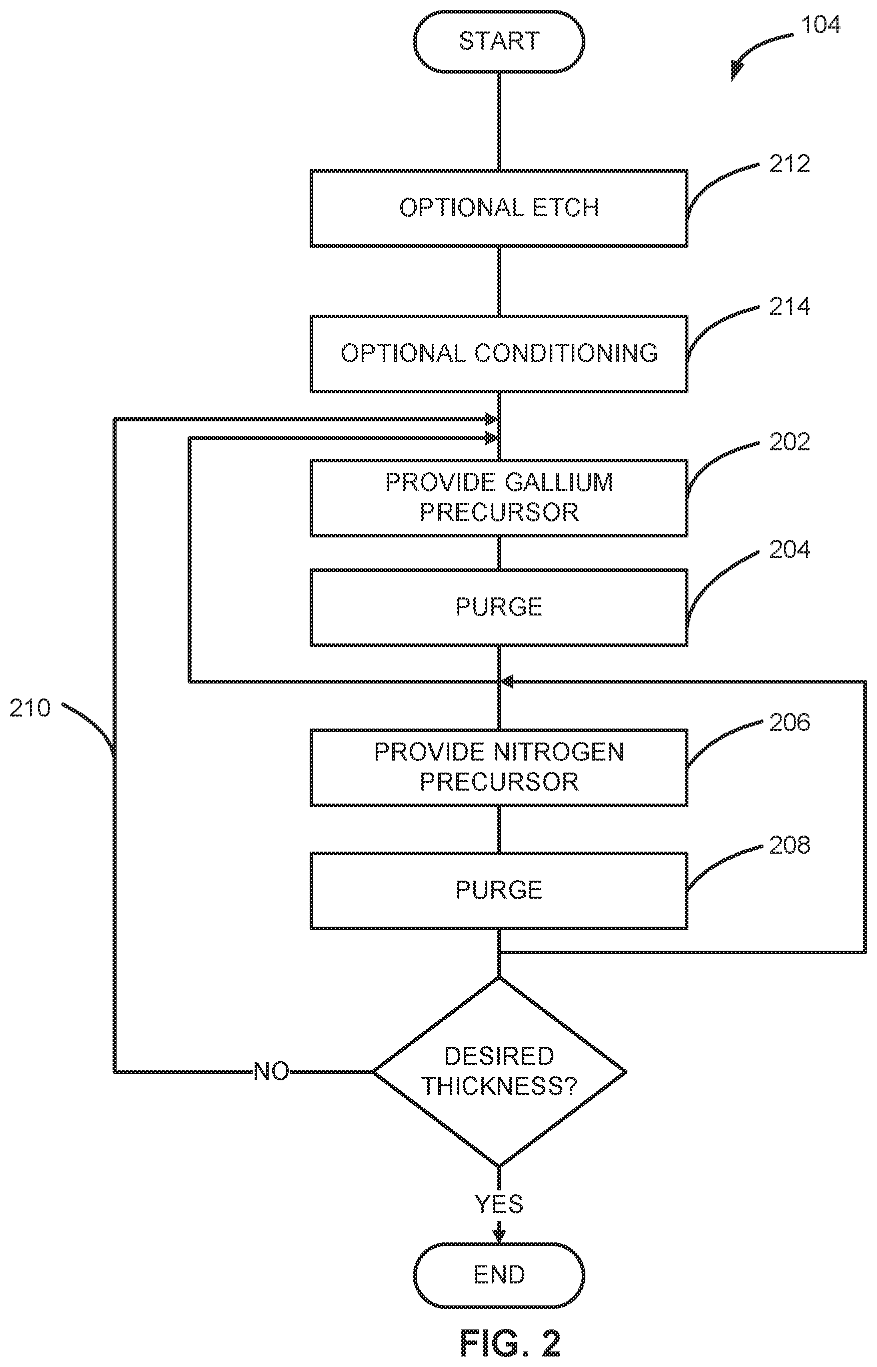
[0033] As illustrated in FIG. 2, step 104 can include a substep of providing a gallium precursor to a reaction chamber (step 202), a substep of purging/removing any unreacted gallium precursor and reaction byproducts from the reaction chamber (step 204), a substep of providing a nitrogen precursor to the reaction chamber (step 206), and a substep of purging/removing any unreacted nitrogen precursor and reaction byproducts from the reaction chamber (step 208). Substeps 202-208 can be referred to simply as steps. Step 104 can also include one or more optional substeps, such as an optional etch step 212 and/or an optional conditioning step 214.
[0034] Steps 202-208 can be repeated (step 210) until a film of desired thickness is formed. Additionally or alternatively, steps 202 and 204 can be repeated one or more times before proceeding to step 206 and/or steps 206 and 208 can be repeated before proceeding to step 202. Further, although illustrated as initiating with providing a gallium precursor step 202, step 104 can alternatively begin with providing a nitrogen precursor step 206 and/or one or more of steps 212, 214.
[0035] Suitable precursors/reactants to deposit gallium nitride include gallium trichloride (GaCl.sub.3), gallium tribromide (GaBr.sub.3), gallium triiodide (GaI.sub.3), trimethylgallium (TMG) and triethylgallium (TEG) as gallium precursors and nitrogen (N.sub.2), ammonia (NH.sub.3) and hydrazine (N.sub.2H.sub.4) as nitrogen precursors, and/or remotely created radicals from Nitrogen (N.sub.2), ammonia (NH.sub.3) and hydrazine (N.sub.2H.sub.4) in such a way that the substrate is not exposed to any plasma or other form of energy used to create the radicals.
[0036] A flow rate of the precursors can vary, depending on, for example, the reaction chamber configuration, a size of the substrate, and/or a number of substrates being processed. By way of example, for a reactor having an interior volume of about 32 cm.sup.3, a flowrate of the gallium precursor during step 202 can be about 0.1 to about 100, or about 5 sccm and a flowrate of the nitrogen precursor during step 206 can be about 1 to about 100, or about 4 sccm. A flowrate of a purge gas, such as, for example, argon during steps 204, 208 for the same reactor volume can range from about 25 sccm to about 150 sccm. A partial pressure of the nitrogen precursor (e.g., NH.sub.3) can be, for example, about 10 to about 15 percent of the total reactor pressure.
[0037] In some embodiments of the disclosure, step 202 includes exposing the substrate to the gallium precursor for a time period of between about 0.01 seconds and about 60 seconds, between about 0.05 seconds and about 10 seconds, or between about 0.1 seconds and about 5 seconds. In some embodiments of the disclosure, step 206 includes exposing the substrate to the nitrogen precursor for a time period of between about 0.01 seconds and about 60 seconds, between about 10 seconds and about 50 seconds, or between about 20 seconds and about 40 seconds. A duration of step 204 can range from about 1 to about 120, about 10 to about 90, or be about 30 seconds. A duration of step 208 can range from about 1 to about 120, about 10 to about 90, or be about 60 seconds. Removal of any excess precursor and/or any reaction byproducts may be facilitated with the aid of a vacuum generated by a pumping system.
[0038] Typically, cyclic deposition--e.g., ALD--of gallium nitride on aluminum nitride or gallium nitride, particularly on features of aluminum nitride or gallium nitride formed by etching layers of the respective materials, may not be selective relative to other material.
[0039] However, silicon nitride has a relatively long incubation period. Therefore, in accordance with some aspects of these embodiments of the disclosure, the second portion comprises silicon nitride.
[0040] The incubation period for nitrogen-terminated material, e.g., NII.sub.x (x=1-2) terminated aluminum nitride or gallium nitride may be relatively low compared to other materials, such as silicon, metal or silicon oxides, nitrides, or oxynitrides. Unfortunately, the NH.sub.x termination of deposited aluminum nitride and/or gallium nitride may be lost due to, for example, oxidation of the material, which can occur as a result of etching the material and/or exposure to an oxidizing environment, such as air. In accordance with exemplary aspects of the illustrated embodiments, aluminum nitride and/or gallium nitride material (e.g., features including the material) is exposed to an environment to provide NH.sub.x termination on the aluminum nitride and/or gallium nitride, preferably selectively on the aluminum nitride or gallium nitride relative to the second portion.
[0041] By way of examples, a NH, NH.sub.2, and/or hydrogen radical flux can be used to selectively condition or provide NH.sub.x termination (step 214) on the first portion including one or more of aluminum nitride or gallium nitride or other material as noted herein, relative to the second portion. The radical flux can be formed from the precursor gases using, for example, a remote plasma, hot wire or any other suitable method. Optional conditioning step 214 can be performed in the same reaction chamber used to perform step 104 and without a vacuum break between the conditioning step and the deposition steps. Further, conditioning step 214 can be performed at the same (or different) temperature and/or same (or different) pressure as the deposition steps.
[0042] To further facilitate selective deposition, step 104 can include optional etch step 212 to etch a surface of the one or more of aluminum nitride and gallium nitride prior to exposing the surface to the radical flux and/or other conditioning. The optional etch step 212 can be performed using, for example, atomic hydrogen or sputtering by argon ions.
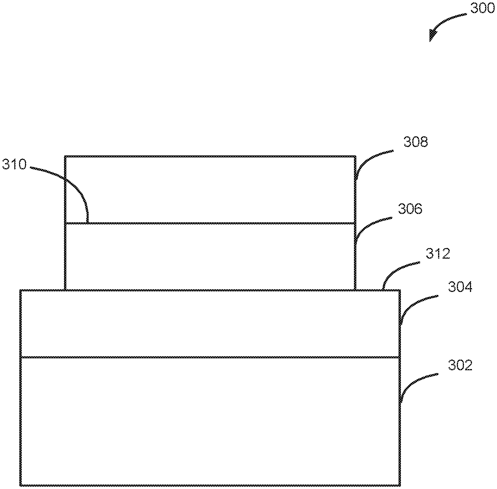
[0043] Turning now to FIG. 3, a structure 300, formed according to exemplary methods described herein, is illustrated. Structure 300 includes a substrate 302, first layer 304, a second layer 306 including one or more of aluminum nitride and gallium nitride (or other boron group (Group III) nitrides, such as BN, InN, or transition metal(s)), and a gallium nitride layer 308. As illustrated, prior to forming gallium nitride layer 308, structure 300 includes a surface including a first portion 310 that includes one or more of aluminum nitride and gallium nitride (or other material as noted herein) and a second portion 312 that includes other material, such as silicon, an oxide, a nitride, or an oxynitride. By way of particular examples, second portion 312 can include hafnium oxide, zirconium oxide, aluminum oxide, or other metal or metalloid oxide, nitride or oxynitride. Gallium nitride layer 308 is selectively deposited onto a first surface 310, relative to second surface 312, using one or more methods described herein. Gallium nitride layer 308 may be monocrystalline or polycrystalline.
[0044] As noted above, first portion 310 can be formed by depositing a layer of, for example, aluminum nitride or gallium nitride, patterning the layer, and etching the layer to form first portion 310. The aluminum nitride or gallium nitride layer for first portion 310 can be formed using a cyclic deposition process, ALD, chemical vapor deposition (CVD), molecular beam epitaxy (MBE), or physical deposition (PVD) techniques. Suitable precursors for a cyclic deposition process, ALD and CVD for depositing aluminum nitride include trimethylaluminum (TMA), triethylaluminium (TEA) and aluminumtrichloride (AlCl.sub.3) and any of the nitrogen precursors noted herein. Suitable precursors for cyclic deposition, ALD and CVD for depositing gallium nitride include TMG, TEG, GaCl.sub.3, and any of the nitrogen precursors noted herein.
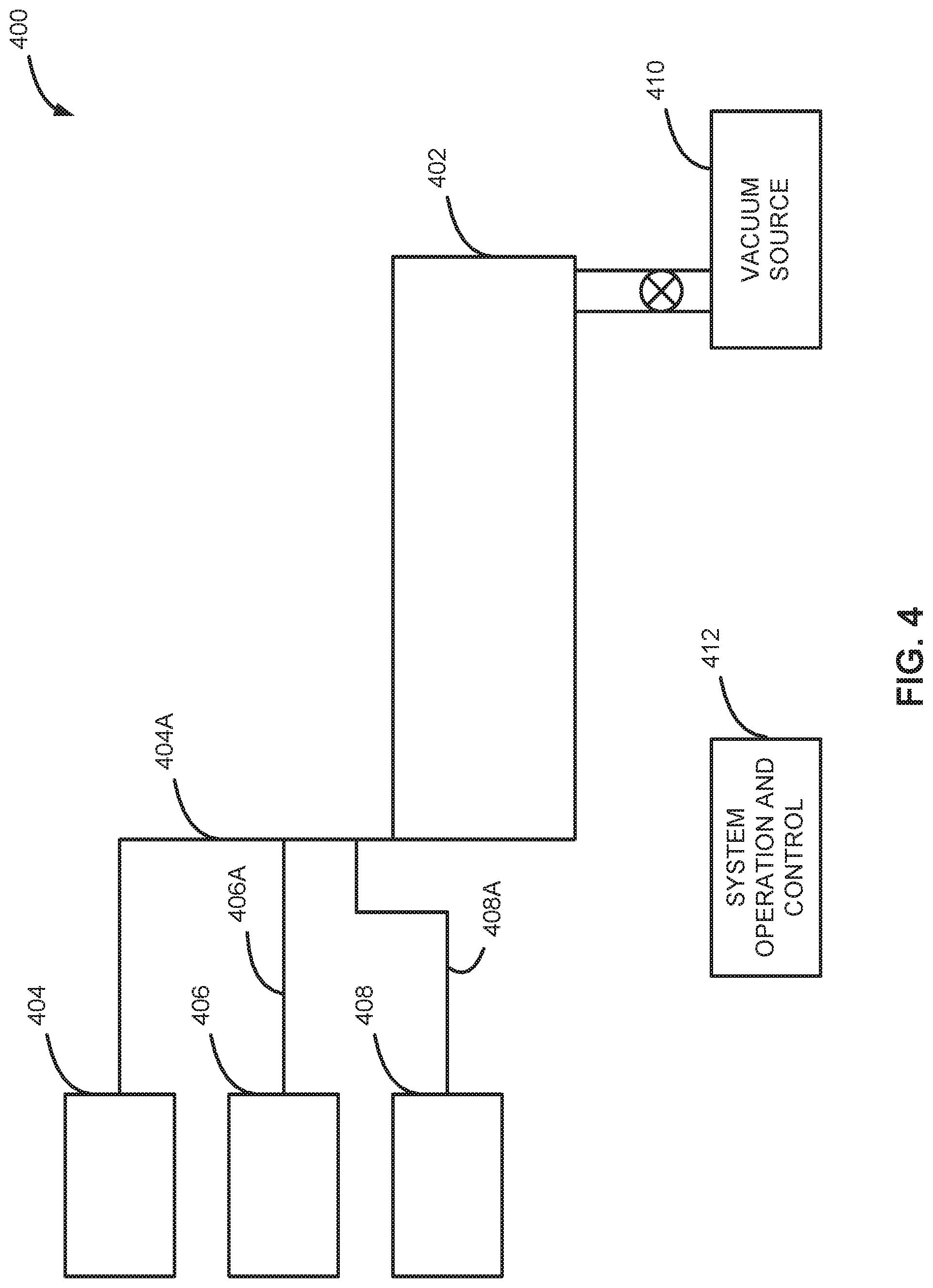
[0045] FIG. 4 illustrates a system 400 configured for selectively forming the gallium nitride on a surface of a substrate in accordance with additional examples of the disclosure. System 400 includes a reaction chamber 402, a first reactant/precursor source 404, a second reactant/precursor source 406, one or more purge gas sources 408, a vacuum source 410, and a system operation and control 412. A suitable system to perform the methods described herein is available from ASM International, under the name Pulsar.RTM..
[0046] Reaction chamber 402 can include a mechanism for retaining a substrate (not shown) under predetermined pressure, temperature, and ambient conditions, and for selectively exposing the substrate to various gasses. Exemplary pressures and temperatures are provided above.
[0047] Precursor source 404 may be coupled by conduits or other appropriate means 404A to the reaction chamber 402, and may further couple to a manifold, valve control system, mass flow control system, or mechanism to control a gaseous precursor originating from the precursor source 404. Similarly, precursor source 406 may be coupled by conduits or other appropriate means 406A to the reaction chamber 402, and may further couple to a manifold, valve control system, mass flow control system, or mechanism to control a gaseous precursor originating from the precursor source 406.
[0048] A precursor (not shown) supplied by the precursor source 404 and/or precursor source 406 may be liquid or solid under room temperature and standard atmospheric pressure conditions. Such a precursor may be vaporized within a reactant source vacuum vessel, which may be maintained at or above a vaporizing temperature within a precursor source chamber. In such embodiments, the vaporized precursor may be transported with a carrier gas (e.g., an inactive or inert gas) and then fed into the reaction chamber 402 through conduit 404A or conduit 404B. In other embodiments, the precursor may be a vapor under standard conditions. In such embodiments, the precursor does not need to be vaporized and may not require a carrier gas. For example, in one embodiment the precursor may be stored in a gas cylinder.
[0049] Purge gas source 408 may also be coupled to the reaction chamber 402 via conduit 408A and selectively supply various inert or noble gasses to the reaction chamber 402 to assist with the removal of precursor gas or waste gasses from the reaction chamber. The various inert or noble gasses that may be supplied may originate from a solid, liquid or stored gaseous form.
[0050] Vacuum source can include a dry and/or a turbomolecular pump.
[0051] System operation and control mechanism 412 can provide electronic circuitry and mechanical components to selectively operate valves, manifolds, pumps and other equipment included in the reaction system 400. Such circuitry and components operate to introduce precursors, purge gasses from the respective precursor sources 404, 406 and purge gas source 408. The system operation and control mechanism 412 also controls timing of gas pulse sequences, temperature of the substrate and reaction chamber, and pressure of the reaction chamber and various other operations necessary to provide proper operation of the reaction system 400. The operation and control mechanism 410 can include control software and electrically or pneumatically controlled valves to control flow of precursors, reactants and purge gasses into and out of the reaction chamber 402. The control system can include modules such as a software or hardware component, e.g., a FPGA or ASIC, which performs certain tasks. A module can advantageously be configured to reside on the addressable storage medium of the control system and be configured to execute one or more processes.
[0052] Although exemplary embodiments of the present disclosure are set forth herein, it should be appreciated that the disclosure is not so limited. Various modifications, variations, and enhancements of the apparatus, assemblies, and systems set forth herein may be made without departing from the spirit and scope of the present disclosure.
[0053] Unless otherwise stated, the subject matter of the present disclosure includes all novel and nonobvious combinations and subcombinations of the various systems, components, and configurations, and other features, functions, acts, and/or properties disclosed herein, as well as any and all equivalents thereof.
* * * * *
D00000
D00001
D00002
D00003
D00004
XML
uspto.report is an independent third-party trademark research tool that is not affiliated, endorsed, or sponsored by the United States Patent and Trademark Office (USPTO) or any other governmental organization. The information provided by uspto.report is based on publicly available data at the time of writing and is intended for informational purposes only.
While we strive to provide accurate and up-to-date information, we do not guarantee the accuracy, completeness, reliability, or suitability of the information displayed on this site. The use of this site is at your own risk. Any reliance you place on such information is therefore strictly at your own risk.
All official trademark data, including owner information, should be verified by visiting the official USPTO website at www.uspto.gov. This site is not intended to replace professional legal advice and should not be used as a substitute for consulting with a legal professional who is knowledgeable about trademark law.