Display Device
WU; SHIH-PING ; et al.
U.S. patent application number 16/367966 was filed with the patent office on 2020-06-18 for display device. The applicant listed for this patent is Quantum Optoelectronics Inc.. Invention is credited to CHI-WEI CHEN, YU-SHENG LIU, MING-HSIEN TSAI, SHIH-PING WU.
| Application Number | 20200192110 16/367966 |
| Document ID | / |
| Family ID | 71073586 |
| Filed Date | 2020-06-18 |


View All Diagrams
| United States Patent Application | 20200192110 |
| Kind Code | A1 |
| WU; SHIH-PING ; et al. | June 18, 2020 |
DISPLAY DEVICE
Abstract
A display device includes an imaging element, a flat surface light source and a polarization beam splitter. The flat surface light source is used for providing plural illumination beams. A normal line of the flat surface light source and a normal line of the imaging element are not perpendicular to each other. The polarization beam splitter is arranged between the flat surface light source and the imaging element, and has a geometric surface. When the illumination beams from the flat surface light source are projected on the geometric surface, the illumination beams are reflected to the imaging element. The imaging beams from the imaging element are transmitted through the geometric surface. Consequently, an image is outputted. An imaging surface of the imaging surface can be irradiated uniformly by the illumination beams on within a specified viewing angle.
| Inventors: | WU; SHIH-PING; (Taipei City, TW) ; LIU; YU-SHENG; (Taipei City, TW) ; CHEN; CHI-WEI; (Taipei City, TW) ; TSAI; MING-HSIEN; (Taipei City, TW) | ||||||||||
| Applicant: |
|
||||||||||
|---|---|---|---|---|---|---|---|---|---|---|---|
| Family ID: | 71073586 | ||||||||||
| Appl. No.: | 16/367966 | ||||||||||
| Filed: | March 28, 2019 |
| Current U.S. Class: | 1/1 |
| Current CPC Class: | H04N 9/3167 20130101; G02B 5/3025 20130101; G02B 27/286 20130101; G02B 5/3033 20130101; G03B 21/2073 20130101; G02F 1/136277 20130101; G02B 27/283 20130101; G02B 5/3016 20130101 |
| International Class: | G02B 27/28 20060101 G02B027/28; G02B 5/30 20060101 G02B005/30 |
Foreign Application Data
| Date | Code | Application Number |
|---|---|---|
| Dec 12, 2018 | TW | 107144823 |
Claims
1. A display device, comprising: an imaging element having an imaging surface for providing an image; a flat surface light source having a light emitting surface for providing plural illumination beams, wherein a normal line of the light emitting surface and a normal line of the imaging surface are not perpendicular to each other; and a polarization beam splitter arranged between the flat surface light source and the imaging element, and having a geometric surface, wherein when at least portions of plural illumination beams in a first polarization state and from the flat surface light source are projected on the geometric surface, the portions of the plural illumination beams in the first polarization state are reflected to the imaging element, wherein after the portions of the plural illumination beams in the first polarization state are projected on the imaging element and exited from the imaging element, the portions of the plural illumination beams in the first polarization state are converted into imaging beams in a second polarization state, wherein at least portions of the imaging beams in the second polarization state are transmitted through the geometric surface, so that the image is outputted.
2. The display device according to claim 1, wherein if a half of a length of a side of the imaging surface is smaller than 2.75 mm, the display device satisfies following mathematic formulae: -0.047385 X.sub.i.sup.2+0.771625 X.sub.i+3.4.ltoreq.Y.sub.i; Y.sub.i.ltoreq.-0.047385 X.sub.i.sup.2+0.771625 X.sub.i+5; Y.sub.i=M.sub.i-N.sub.i; and 69.degree..ltoreq..theta..sub.t.ltoreq.78.degree., wherein X.sub.i is a position of the imaging surface and defined according to a coordinate axis, the coordinate axis is parallel with the side of the imaging surface and perpendicular to the normal line of the imaging surface, M.sub.i is a spacing distance between the position of the imaging surface and the geometric surface along the normal line of the imaging surface, N.sub.i is a spacing distance between the position of the imaging surface and a top surface of the imaging element along the normal line of the imaging surface, and .theta..sub.t is an included angle between the normal line of the imaging surface and the normal line of the light emitting surface.
3. The display device according to claim 2, wherein the display device further satisfies following mathematic formulae (a1).about.(a6): if X.sub.i=0, 3.6.ltoreq.Y.sub.i.ltoreq.3.8; (a1) if X.sub.i=0, 3.8.ltoreq.Y.sub.i.ltoreq.4.0; (a2) if X.sub.i=0, 4.0.ltoreq.Y.sub.i.ltoreq.4.2; (a3) if X.sub.i=0, 4.2.ltoreq.Y.sub.i.ltoreq.4.4; (a4) if X.sub.i=0, 4.4.ltoreq.Y.sub.i.ltoreq.4.6; and (a5) if X.sub.i=0, 4.6.ltoreq.Y.sub.i.ltoreq.4.8. (a6)
4. The display device according to claim 2, wherein the imaging surface has a rectangular shape, and the side of the imaging surface is a short side of the imaging surface.
5. The display device according to claim 1, wherein if a half of a length of a side of the imaging surface is larger than 2.75 mm and smaller than 3.5 mm, the display device satisfies following mathematic formulae: -0.043299 X.sub.i.sup.2+0.745345 X.sub.i+4.ltoreq.Y.sub.i; Y.sub.i.ltoreq.-0.043299 X.sub.i.sup.2+0.745345 X.sub.i+6; Y.sub.i=M.sub.i-N.sub.i; and 68.5.degree..ltoreq..theta..sub.t.ltoreq.82.5.degree.. wherein X.sub.i is a position of the imaging surface and defined according to a coordinate axis, the coordinate axis is parallel with the side of the imaging surface and perpendicular to the normal line of the imaging surface, M.sub.i is a spacing distance between the position of the imaging surface and the geometric surface along the normal line of the imaging surface, N.sub.i is a spacing distance between the position of the imaging surface and a top surface of the imaging element along the normal line of the imaging surface, and .theta..sub.t is an included angle between the normal line of the imaging surface and the normal line of the light emitting surface.
6. The display device according to claim 5, wherein the display device further satisfies following mathematic formulae (b1).about.(b8): if X.sub.i=0, 4.2.ltoreq.Y.sub.i.ltoreq.4.4; (b1) if X.sub.i=0, 4.4.ltoreq.Y.sub.i.ltoreq.4.6; (b2) if X.sub.i=0, 4.6.ltoreq.Y.sub.i.ltoreq.4.8; (b3) if X.sub.i=0, 4.8.ltoreq.Y.sub.i.ltoreq.5.0; (b4) if X.sub.i=0, 5.0.ltoreq.Y.sub.i.ltoreq.5.2; (b5) if X.sub.i=0, 5.2.ltoreq.Y.sub.i.ltoreq.5.4; (b6) if X.sub.i=0, 5.4.ltoreq.Y.sub.i.ltoreq.5.6; and (b7) if X.sub.i=0, 5.6.ltoreq.Y.sub.i.ltoreq.5.8. (b8)
7. The display device according to claim 5, wherein the imaging surface has a rectangular shape, and the side of the imaging surface is a short side of the imaging surface.
8. The display device according to claim 1, wherein the imaging element comprises a top glass cover, an intermediate structure and a circuit board, wherein the intermediate structure is arranged between the top glass cover and the circuit board, the imaging surface is disposed within the intermediate structure, and a top surface of the imaging element is a top surface of the top glass cover.
9. The display device according to claim 1, wherein a position of the imaging surface is defined according to a coordinate axis, and the coordinate axis is parallel with the side of the imaging surface and perpendicular to the normal line of the imaging surface, wherein as the position of the imaging surface is moved along an axial direction of the coordinate axis, a spacing distance between the position of the imaging surface and the geometric surface along the normal line of the imaging surface is increased.
10. The display device according to claim 9, wherein the imaging surface has a rectangular shape, and the side of the imaging surface is a short side of the imaging surface.
11. The display device according to claim 1, wherein the flat surface light source comprises a substrate, plural light emitting diodes and a diffusion plate, wherein the plural light emitting diodes are disposed on the substrate to provide light beams, wherein after the light beams are transmitted through the diffusion plate, a surface light source is generated.
12. The display device according to claim 1, wherein the flat surface light source comprises a light chamber, at least one light emitting diode and a diffusion plate, wherein the at least one light emitting diode is located at a first end of the light chamber, the diffusion plate is located at a second end of the light chamber, and plural light beams from the light emitting diode are transferred within the light chamber, wherein after the light beams are reflected and scattered by an inner surface of the light chamber, the light beams are projected to the diffusion plate, wherein after the light beams are transmitted through the diffusion plate, a surface light source is generated.
13. The display device according to claim 1, wherein the flat surface light source comprises at least one light emitting diode and a light guide plate, wherein after plural light beams from the at least one light emitting diode are introduced into the light guide plate, the plural light beams are guided by the light guide plate, wherein after the plural light beams are transmitted through the light guide plate, a surface light source is generated.
14. The display device according to claim 1, wherein the flat surface light source further comprises a polarizer, wherein after plural light beams are transmitted through the polarizer, the plural illumination beams in the first polarization state are generated.
15. The display device according to claim 1, wherein the imaging element is a LCoS (liquid crystal on silicon) element; and/or the polarization beam splitter is a reflective polarizer or a dual brightness enhancement film.
16. The display device according to claim 1, wherein the polarization beam splitter has a thin film structure.
17. A display device, comprising: an imaging element having an imaging surface for providing an image; a flat surface light source providing plural illumination beams; and a polarization beam splitter arranged between the flat surface light source and the imaging element, wherein when at least portions of plural illumination beams in a first polarization state and from the flat surface light source are projected on the polarization beam splitter, the portions of the plural illumination beams in the first polarization state are reflected to the imaging element, wherein at least portions of imaging beams in the second polarization state and from the imaging element are transmitted through the polarization beam splitter, so that the image is outputted, wherein a position of the imaging surface is defined according to a coordinate axis, and the coordinate axis is parallel with a side of the imaging surface and perpendicular to a normal line of the imaging surface, wherein as the position of the imaging surface is moved along an axial direction of the coordinate axis, a spacing distance between the position of the imaging surface and the geometric surface along the normal line of the imaging surface is increased.
18. The display device according to claim 17, wherein the flat surface light source has a light emitting surface, wherein a normal line of the light emitting surface and the normal line of the imaging surface are not perpendicular to each other.
19. The display device according to claim 18, wherein if a half of a length of the side of the imaging surface is smaller than 2.75 mm, the display device satisfies following mathematic formulae: -0.047385 X.sub.i.sup.2+0.771625 X.sub.i+3.4.ltoreq.Y.sub.i; Y.sub.i.ltoreq.-0.047385 X.sub.i.sup.2+0.771625 X.sub.i+5; Y.sub.i=M.sub.i-N.sub.i; and 69.degree..ltoreq..theta..sub.t.ltoreq.78.degree., wherein X.sub.i is the position of the imaging surface and defined according to the coordinate axis, M.sub.i is the spacing distance between the position of the imaging surface and the polarization beam splitter along the normal line of the imaging surface, N.sub.i is a spacing distance between the position of the imaging surface and a top surface of the imaging element along the normal line of the imaging surface, and .theta..sub.t is an included angle between the normal line of the imaging surface and the normal line of the light emitting surface.
20. The display device according to claim 19, wherein the display device satisfies following mathematic formulae (a1).about.(a6): if X.sub.i=0, 3.6.ltoreq.Y.sub.i.ltoreq.3.8; (a1) if X.sub.i=0, 3.8.ltoreq.Y.sub.i.ltoreq.4.0; (a2) if X.sub.i=0, 4.0.ltoreq.Y.sub.i.ltoreq.4.2; (a3) if X.sub.i=0, 4.2.ltoreq.Y.sub.i.ltoreq.4.4; (a4) if X.sub.i=0, 4.4.ltoreq.Y.sub.i.ltoreq.4.6; and (a5) if X.sub.i=0, 4.6.ltoreq.Y.sub.i.ltoreq.4.8. (a6)
21. The display device according to claim 18, wherein if a half of a length of the side of the imaging surface is larger than 2.75 mm and smaller than 3.5 mm, the display device satisfies following mathematic formulae: -0.043299 X.sub.i.sup.2+0.745345 X.sub.i+4.ltoreq.Y.sub.i; Y.sub.i.ltoreq.-0.043299 X.sub.i.sup.2+0.745345 X.sub.i+6; Y.sub.i=M.sub.i-N.sub.i; and 68.5.degree..ltoreq..theta..sub.t.ltoreq.82.5.degree.. wherein X.sub.i is the position of the imaging surface and defined according to the coordinate axis, M.sub.i is the spacing distance between the position of the imaging surface and the polarization beam splitter along the normal line of the imaging surface, N.sub.i is a spacing distance between the position of the imaging surface and a top surface of the imaging element along the normal line of the imaging surface, and .theta..sub.t is an included angle between the normal line of the imaging surface and the normal line of the light emitting surface.
22. The display device according to claim 21, wherein the display device further satisfies following mathematic formulae (b1).about.(b8): if X.sub.i=0, 4.2.ltoreq.Y.sub.i.ltoreq.4.4; (b1) if X.sub.i=0, 4.4.ltoreq.Y.sub.i.ltoreq.4.6; (b2) if X.sub.i=0, 4.6.ltoreq.Y.sub.i.ltoreq.4.8; (b3) if X.sub.i=0, 4.8.ltoreq.Y.sub.i.ltoreq.5.0; (b4) if X.sub.i=0, 5.0.ltoreq.Y.sub.i.ltoreq.5.2; (b5) if X.sub.i=0, 5.2.ltoreq.Y.sub.i.ltoreq.5.4; (b6) if X.sub.i=0, 5.4.ltoreq.Y.sub.i.ltoreq.5.6; and (b7) if X.sub.i=0, 5.6.ltoreq.Y.sub.i.ltoreq.5.8. (b8)
23. The display device according to claim 17, wherein the imaging element comprises a top glass cover, an intermediate structure and a circuit board, wherein the intermediate structure is arranged between the top glass cover and the circuit board, the imaging surface is disposed within the intermediate structure, and a top surface of the imaging element is a top surface of the top glass cover.
24. The display device according to claim 17, wherein the flat surface light source comprises a substrate, plural light emitting diodes and a diffusion plate, wherein the plural light emitting diodes are disposed on the substrate to provide light beams, wherein after the light beams are transmitted through the diffusion plate, a surface light source is generated.
25. The display device according to claim 17, wherein the flat surface light source comprises a light chamber, at least one light emitting diode and a diffusion plate, wherein the at least one light emitting diode is located at a first end of the light chamber, the diffusion plate is located at a second end of the light chamber, and plural light beams from the light emitting diode are transferred within the light chamber, wherein after the light beams are reflected and scattered by an inner surface of the light chamber, the light beams are projected to the diffusion plate, wherein after the light beams are transmitted through the diffusion plate, a surface light source is generated.
26. The display device according to claim 17, wherein the flat surface light source comprises at least one light emitting diode and a light guide plate, wherein after plural light beams from the at least one light emitting diode are introduced into the light guide plate, the plural light beams are guided by the light guide plate, wherein after the plural light beams are transmitted through the light guide plate, a surface light source is generated.
27. The display device according to claim 17, wherein the flat surface light source further comprises a polarizer, wherein after plural light beams are transmitted through the polarizer, the plural illumination beams in the first polarization state are generated.
28. The display device according to claim 17, wherein the imaging surface has a rectangular shape, and the side of the imaging surface is a short side of the imaging surface.
29. The display device according to claim 17, wherein the imaging element is a LCoS (liquid crystal on silicon) element; and/or the polarization beam splitter is a reflective polarizer or a dual brightness enhancement film.
30. The display device according to claim 17, wherein the polarization beam splitter has a thin film structure.
Description
FIELD OF THE INVENTION
[0001] The present invention relates to the field of an optical technology, and more particularly to a display device.
BACKGROUND OF THE INVENTION
[0002] With the advent of the multimedia and Internet eras, the exchange of images and information has become increasingly rapid and various new display technologies have been emerged. With the development of these display technologies, a variety of display technologies have been continuously proposed to solve the problems about various display applications.
[0003] Nowadays, the technology of reflective liquid crystal displays becomes one of the development mainstreams of the display technology because the reflective liquid crystal displays have some advantages such as low power consumption and visibility under sunlight. The illumination system for providing light beams to the reflective liquid crystal display is very important for the imaging quality of the reflective liquid crystal display. For example, some techniques about the illumination system of the reflective liquid crystal display are disclosed in U.S. Pat. Nos. 6,433,935, 6,976,759 and 7,529,029.
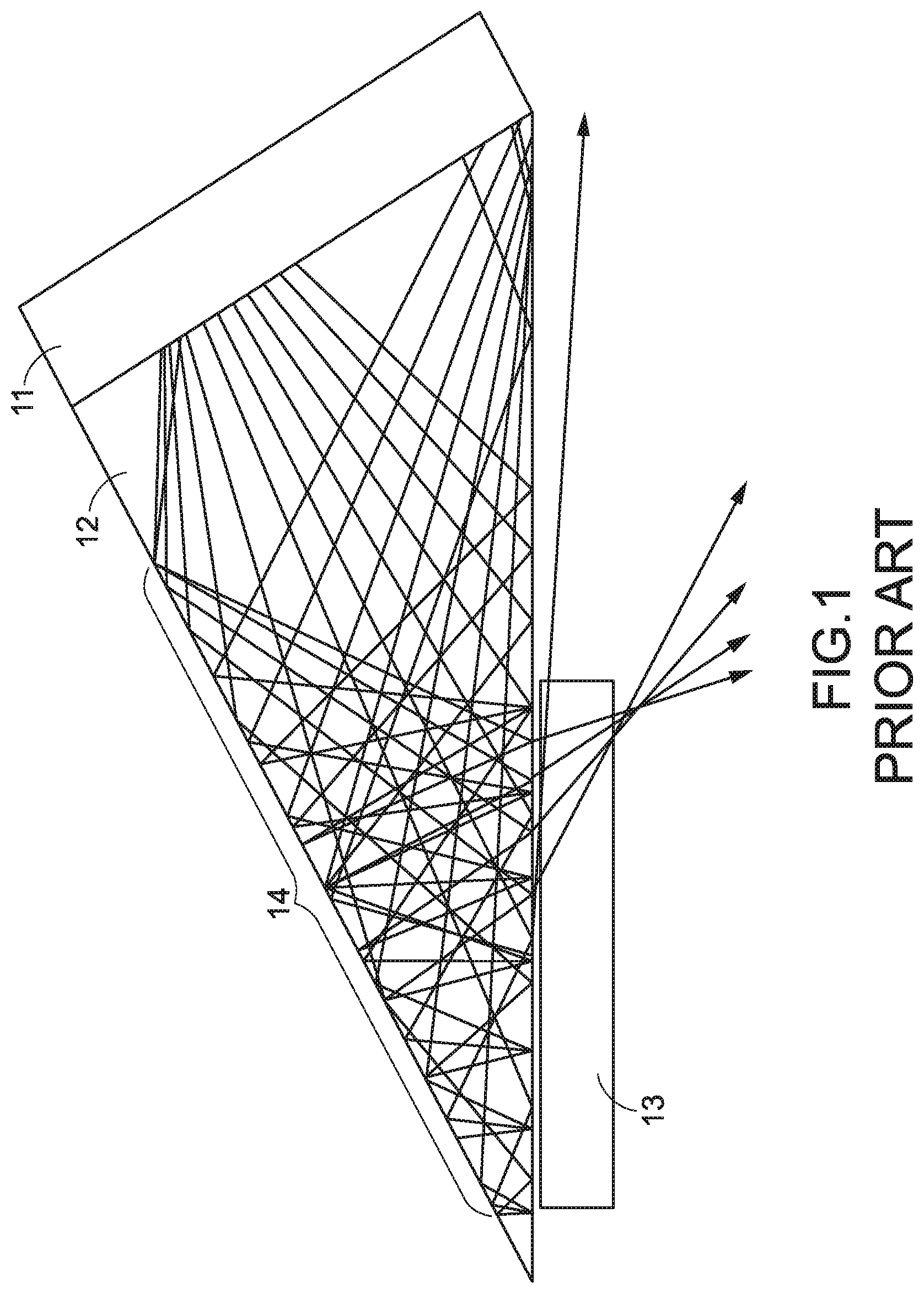
[0004] FIG. 1 schematically illustrates an illumination system disclosed in U.S. Pat. No. 6,433,935. After a light beam from a light source 11 is introduced into a wedge-shaped prism 12, the light beam undergoes a total internal reflection within the wedge-shaped prism 12. Consequently, the projection area and the viewing angle of a reflective liquid crystal display are expanded. The associated technique is disclosed in the patent specification, and detailed descriptions thereof are omitted. However, this illumination system still has some drawbacks. For example, chromatic aberration is formed on an image exit surface 14, the optical axis is skewed and the image is distorted. These problems are detrimental to the subsequent imaging applications.
[0005] FIG. 2 schematically illustrates a polarization beam splitter (PBS) assembly disclosed in U.S. Pat. No. 6,976,759. After an illumination beam from a light source is introduced into a prism surface 20, the illumination beam 21 is projected on the prism surface 22 and undergoes a total internal reflection. Consequently, the illumination beam 21 is reflected to a polarization splitting surface 23. When the illumination beam 21 is projected on the polarization splitting surface 23, the illumination beam 21 is reflected to the prism surface 22 by the polarization splitting surface 23. Then, the illumination beam 21 is transmitted through the prism surface 22 and projected on an imaging surface of a reflective light valve 27. When the illumination beam 21 is projected on the imaging surface of the reflective light valve 27, the illumination beam 21 is converted into an imaging beam 26. After the imaging beam 26 is transmitted through the prism surface 22, the polarization splitting surface 23 and a compensation prism 24 sequentially, the imaging beam 26 is outputted. The compensation prism 24 is used for correcting the optical axis. Consequently, the imaging beam 26 is outputted along a normal direction of the reflective light valve 27. However, the arrangement of the compensation prism 24 increases the thickness of the overall PBS assembly. In addition, the distance between the imaging surface of the reflective light valve 27 and a light exit surface 25 is increased. In other words, it is difficult to minimize the PBS assembly and install the PBS assembly in a short-focus optical system.
[0006] FIG. 3 schematically illustrates an image display system disclosed in U.S. Pat. No. 7,529,029. A polarization beam splitter 32 of the image display system 30 comprises a curvy surface 34 and a curvy surface 35. By the polarization beam splitter 32, an illumination beam 36 from a light source 31 is guided along an optical path to a reflective light valve 33 and an imaging beam 36' is guided from the reflective light valve 33. In other words, the image display system integrates an illumination element and an imaging element. However, the combination of the illumination element and the imaging element needs the curvy prism with complicated curvy surfaces. For achieving the desired imaging quality, the curvy prism needs high precision and small tolerance range.
[0007] Therefore, the existing display device needs to be further improved.
SUMMARY OF THE INVENTION
[0008] For solving the drawbacks of the conventional technologies, the present invention provides a display device. An imaging surface of an imaging surface can be uniformly irradiated by the illumination beams within a specified viewing angle. Moreover, the process of producing the components of the display device is simplified, and the display device is cost-effective.
[0009] In accordance with an aspect of the present invention, a display device is provided. The display device includes an imaging element, a flat surface light source and a polarization beam splitter. The imaging element has an imaging surface for providing an image. The flat surface light source has a light emitting surface for providing plural illumination beams. A normal line of the light emitting surface and a normal line of the imaging surface are not perpendicular to each other. The polarization beam splitter is arranged between the flat surface light source and the imaging element, and has a geometric surface. When at least portions of plural illumination beams in a first polarization state and from the flat surface light source are projected on the geometric surface, the portions of the plural illumination beams in the first polarization state are reflected to the imaging element. After the portions of the plural illumination beams in the first polarization state are projected on the imaging element and exited from the imaging element, the portions of the plural illumination beams in the first polarization state are converted into imaging beams in a second polarization state. Moreover, at least portions of the imaging beams in the second polarization state are transmitted through the geometric surface, so that the image is outputted.
[0010] In an embodiment, if a half of a length of a side of the imaging surface is smaller than 2.75 mm, the display device satisfies following mathematic formulae:
-0.047385 X.sub.i.sup.2+0.771625 X.sub.i+3.4.ltoreq.Y.sub.i;
Y.sub.i.ltoreq.-0.047385 X.sub.i.sup.2+0.771625 X.sub.i+5;
Y.sub.i=M.sub.i-N.sub.i; and
69.degree..ltoreq..theta..sub.t.ltoreq.78.degree.,
wherein X.sub.i is a position of the imaging surface and defined according to a coordinate axis, the coordinate axis is parallel with the side of the imaging surface and perpendicular to the normal line of the imaging surface, M.sub.i is a spacing distance between the position of the imaging surface and the geometric surface along the normal line of the imaging surface, N.sub.i is a spacing distance between the position of the imaging surface and a top surface of the imaging element along the normal line of the imaging surface, and .theta..sub.t is an included angle between the normal line of the imaging surface and the normal line of the light emitting surface.
[0011] In an embodiment, the display device further satisfies following mathematic formulae (a1).about.(a6):
if X.sub.i=0, 3.6.ltoreq.Y.sub.i.ltoreq.3.8; (a1)
if X.sub.i=0, 3.8.ltoreq.Y.sub.i.ltoreq.4.0; (a2)
if X.sub.i=0, 4.0.ltoreq.Y.sub.i.ltoreq.4.2; (a3)
if X.sub.i=0, 4.2.ltoreq.Y.sub.i.ltoreq.4.4; (a4)
if X.sub.i=0, 4.4.ltoreq.Y.sub.i.ltoreq.4.6; and (a5)
if X.sub.i=0, 4.6.ltoreq.Y.sub.i.ltoreq.4.8. (a6)
[0012] In an embodiment, if a half of a length of a side of the imaging surface is larger than 2.75 mm and smaller than 3.5 mm, the display device satisfies following mathematic formulae:
-0.043299 X.sub.i.sup.2+0.745345 X.sub.i+4.ltoreq.Y.sub.i;
Y.sub.i.ltoreq.-0.043299 X.sub.i.sup.2+0.745345 X.sub.i+6;
Y.sub.i=M.sub.i-N.sub.i; and
68.5.degree..ltoreq..theta..sub.t.ltoreq.82.5.degree..
wherein X.sub.i is a position of the imaging surface and defined according to a coordinate axis, the coordinate axis is parallel with the side of the imaging surface and perpendicular to the normal line of the imaging surface, M.sub.i is a spacing distance between the position of the imaging surface and the geometric surface along the normal line of the imaging surface, N.sub.i is a spacing distance between the position of the imaging surface and a top surface of the imaging element along the normal line of the imaging surface, and .theta..sub.t is an included angle between the normal line of the imaging surface and the normal line of the light emitting surface.
[0013] In an embodiment, the display device further satisfies following mathematic formulae (b1).about.(b8):
if X.sub.i=0, 4.2.ltoreq.Y.sub.i.ltoreq.4.4; (b1)
if X.sub.i=0, 4.4.ltoreq.Y.sub.i.ltoreq.4.6; (b2)
if X.sub.i=0, 4.6.ltoreq.Y.sub.i.ltoreq.4.8; (b3)
if X.sub.i=0, 4.8.ltoreq.Y.sub.i.ltoreq.5.0; (b4)
if X.sub.i=0, 5.0.ltoreq.Y.sub.i.ltoreq.5.2; (b5)
if X.sub.i=0, 5.2.ltoreq.Y.sub.i.ltoreq.5.4; (b6)
if X.sub.i=0, 5.4.ltoreq.Y.sub.i.ltoreq.5.6; and (b7)
if X.sub.i=0, 5.6.ltoreq.Y.sub.i.ltoreq.5.8. (b8)
[0014] In an embodiment, the imaging element includes a top glass cover, an intermediate structure and a circuit board. The intermediate structure is arranged between the top glass cover and the circuit board. The imaging surface is disposed within the intermediate structure. A top surface of the imaging element is a top surface of the top glass cover.
[0015] In an embodiment, a position of the imaging surface is defined according to a coordinate axis, and the coordinate axis is parallel with the side of the imaging surface and perpendicular to the normal line of the imaging surface. As the position of the imaging surface is moved along an axial direction of the coordinate axis, a spacing distance between the position of the imaging surface and the geometric surface along the normal line of the imaging surface is increased.
[0016] In an embodiment, the imaging surface has a rectangular shape, and the side of the imaging surface is a short side of the imaging surface.
[0017] In an embodiment, the flat surface light source includes a substrate, plural light emitting diodes and a diffusion plate. The plural light emitting diodes are disposed on the substrate to provide light beams. After the light beams are transmitted through the diffusion plate, a surface light source is generated.
[0018] In an embodiment, the flat surface light source includes a light chamber, at least one light emitting diode and a diffusion plate. The at least one light emitting diode is located at a first end of the light chamber. The diffusion plate is located at a second end of the light chamber. Moreover, plural light beams from the light emitting diode are transferred within the light chamber. After the light beams are reflected and scattered by an inner surface of the light chamber, the light beams are projected to the diffusion plate. After the light beams are transmitted through the diffusion plate, a surface light source is generated.
[0019] In an embodiment, the flat surface light source includes at least one light emitting diode and a light guide plate. After plural light beams from the at least one light emitting diode are introduced into the light guide plate, the plural light beams are guided by the light guide plate. After the plural light beams are transmitted through the light guide plate, a surface light source is generated.
[0020] In an embodiment, the flat surface light source further includes a polarizer. After the plural light beams are transmitted through the polarizer, the plural illumination beams in the first polarization state are generated.
[0021] In an embodiment, the imaging element is a LCoS (liquid crystal on silicon) element.
[0022] In an embodiment, the polarization beam splitter is a reflective polarizer or a dual brightness enhancement film.
[0023] In an embodiment, the polarization beam splitter has a thin film structure.
[0024] In accordance with an aspect of the present invention, a display device is provided. The display device includes an imaging element, a flat surface light source and a polarization beam splitter. The imaging element has an imaging surface for providing an image. The flat surface light source provides plural illumination beams. The polarization beam splitter is arranged between the flat surface light source and the imaging element. When at least portions of plural illumination beams in a first polarization state and from the flat surface light source are projected on the polarization beam splitter, the portions of the plural illumination beams in the first polarization state are reflected to the imaging element. Moreover, at least portions of imaging beams in the second polarization state and from the imaging element are transmitted through the polarization beam splitter, so that the image is outputted. A position of the imaging surface is defined according to a coordinate axis. The coordinate axis is parallel with a side of the imaging surface and perpendicular to a normal line of the imaging surface. As the position of the imaging surface is moved along an axial direction of the coordinate axis, a spacing distance between the position of the imaging surface and the geometric surface along the normal line of the imaging surface is increased.
[0025] In an embodiment, the flat surface light source has a light emitting surface. Moreover, a normal line of the light emitting surface and the normal line of the imaging surface are not perpendicular to each other.
[0026] In an embodiment, if a half of a length of the side of the imaging surface is smaller than 2.75 mm, the display device satisfies following mathematic formulae:
-0.047385 X.sub.i.sup.2+0.771625 X.sub.i+3.4.ltoreq.Y.sub.i;
Y.sub.i.ltoreq.-0.047385 X.sub.i.sup.2+0.771625 X.sub.i+5;
Y.sub.i=M.sub.i-N.sub.i; and
69.degree..ltoreq..theta..sub.t.ltoreq.78.degree.,
wherein X.sub.i is the position of the imaging surface and defined according to the coordinate axis, M.sub.i is the spacing distance between the position of the imaging surface and the polarization beam splitter along the normal line of the imaging surface, N.sub.i is a spacing distance between the position of the imaging surface and a top surface of the imaging element along the normal line of the imaging surface, and .theta..sub.t is an included angle between the normal line of the imaging surface and the normal line of the light emitting surface.
[0027] In an embodiment, the display device further satisfies following mathematic formulae (a1).about.(a6):
if X.sub.i=0, 3.6.ltoreq.Y.sub.i.ltoreq.3.8; (a1)
if X.sub.i=0, 3.8.ltoreq.Y.sub.i.ltoreq.4.0; (a2)
if X.sub.i=0, 4.0.ltoreq.Y.sub.i.ltoreq.4.2; (a3)
if X.sub.i=0, 4.2.ltoreq.Y.sub.i.ltoreq.4.4; (a4)
if X.sub.i=0, 4.4.ltoreq.Y.sub.i.ltoreq.4.6; and (a5)
if X.sub.i=0, 4.6.ltoreq.Y.sub.i.ltoreq.4.8. (a6)
[0028] In an embodiment, if a half of a length of the side of the imaging surface is larger than 2.75 mm and smaller than 3.5 mm, the display device satisfies following mathematic formulae:
-0.043299 X.sub.i.sup.2+0.745345 X.sub.i+4.ltoreq.Y.sub.i;
Y.sub.i.ltoreq.-0.043299 X.sub.i.sup.2+0.745345 X.sub.i+6;
Y.sub.i=M.sub.i-N.sub.i; and
68.5.degree..ltoreq..theta..sub.t.ltoreq.82.5.degree..
wherein X.sub.i is the position of the imaging surface and defined according to the coordinate axis, M.sub.i is the spacing distance between the position of the imaging surface and the polarization beam splitter along the normal line of the imaging surface, N.sub.i is a spacing distance between the position of the imaging surface and a top surface of the imaging element along the normal line of the imaging surface, and .theta..sub.t is an included angle between the normal line of the imaging surface and the normal line of the light emitting surface.
[0029] In an embodiment, the display device further satisfies following mathematic formulae (b1).about.(b8):
if X.sub.i=0, 4.2.ltoreq.Y.sub.i.ltoreq.4.4; (b1)
if X.sub.i=0, 4.4.ltoreq.Y.sub.i.ltoreq.4.6; (b2)
if X.sub.i=0, 4.6.ltoreq.Y.sub.i.ltoreq.4.8; (b3)
if X.sub.i=0, 4.8.ltoreq.Y.sub.i.ltoreq.5.0; (b4)
if X.sub.i=0, 5.0.ltoreq.Y.sub.i.ltoreq.5.2; (b5)
if X.sub.i=0, 5.2.ltoreq.Y.sub.i.ltoreq.5.4; (b6)
if X.sub.i=0, 5.4.ltoreq.Y.sub.i.ltoreq.5.6; and (b7)
if X.sub.i=0, 5.6.ltoreq.Y.sub.i.ltoreq.5.8. (b8)
[0030] In an embodiment, the imaging element includes a top glass cover, an intermediate structure and a circuit board. The intermediate structure is arranged between the top glass cover and the circuit board. The imaging surface is disposed within the intermediate structure. A top surface of the imaging element is a top surface of the top glass cover.
[0031] In an embodiment, the flat surface light source includes a substrate, plural light emitting diodes and a diffusion plate. The plural light emitting diodes are disposed on the substrate to provide light beams. After the light beams are transmitted through the diffusion plate, a surface light source is generated.
[0032] In an embodiment, the flat surface light source includes a light chamber, at least one light emitting diode and a diffusion plate. The at least one light emitting diode is located at a first end of the light chamber. The diffusion plate is located at a second end of the light chamber. Moreover, plural light beams from the light emitting diode are transferred within the light chamber. After the light beams are reflected and scattered by an inner surface of the light chamber, the light beams are projected to the diffusion plate. After the light beams are transmitted through the diffusion plate, a surface light source is generated.
[0033] In an embodiment, the flat surface light source includes at least one light emitting diode and a light guide plate. After plural light beams from the at least one light emitting diode are introduced into the light guide plate, the plural light beams are guided by the light guide plate. After the plural light beams are transmitted through the light guide plate, a surface light source is generated.
[0034] In an embodiment, the flat surface light source further includes a polarizer. After the plural light beams are transmitted through the polarizer, the plural illumination beams in the first polarization state are generated.
[0035] In an embodiment, the imaging surface has a rectangular shape, and the side of the imaging surface is a short side of the imaging surface.
[0036] In an embodiment, the imaging element is a LCoS (liquid crystal on silicon) element.
[0037] In an embodiment, the polarization beam splitter is a reflective polarizer or a dual brightness enhancement film.
[0038] In an embodiment, the polarization beam splitter has a thin film structure
[0039] From the above descriptions, the present invention provides the display device. The distance between the geometric surface of the polarization beam splitter and the top glass cover of the imaging element has a specified distribution, and the flat surface light source has a specified inclination angle. Consequently, the imaging surface of the imaging element can be irradiated uniformly by the illumination beams from the flat surface light source within a specified viewing angle. Moreover, since the distance between the imaging element and the polarization beam splitter is shortened, the overall thickness and volume of the display device are reduced. It is not necessary to use the injection molding process or the grinding process of forming the precise optical element to produce the polarization beam splitter of the present invention. In addition, the display device is not equipped with additional precise optical elements. Consequently, the process of producing the components of the display device is simplified, and the display device is cost-effective. In other words, the display device is industrially valuable.
[0040] The above objects and advantages of the present invention will become more readily apparent to those ordinarily skilled in the art after reviewing the following detailed description and accompanying drawings, in which:
BRIEF DESCRIPTION OF THE DRAWINGS
[0041] FIG. 1 schematically illustrates an illumination system disclosed in U.S. Pat. No. 6,433,935;
[0042] FIG. 2 schematically illustrates a polarization beam splitter (PBS) assembly disclosed in U.S. Pat. No. 6,976,759;
[0043] FIG. 3 schematically illustrates an image display system disclosed in U.S. Pat. No. 7,529,029;
[0044] FIG. 4 is a schematic perspective view illustrating a display device according to an embodiment of the present invention;
[0045] FIG. 5 schematically illustrates an imaging element of the display device as shown in FIG. 4 and the viewing angles of plural pixels on an imaging surface of the imaging element;
[0046] FIG. 6 schematically illustrates the optical paths of the display device as shown in FIG. 4;
[0047] FIG. 7 schematically illustrates a first exemplary flat surface light source used in the display device as shown in FIG. 4;
[0048] FIG. 8 is a schematic perspective view illustrating a portion of the flat surface light source as shown in FIG. 7;
[0049] FIG. 9 schematically illustrates a second exemplary flat surface light source used in the display device as shown in FIG. 4;
[0050] FIG. 10 schematically illustrates a third exemplary flat surface light source used in the display device as shown in FIG. 4;
[0051] FIG. 11 schematically illustrates the geometric concepts of the display device as shown in FIG. 4 according to a coordinate system; and
[0052] FIG. 12 schematically illustrates plural positions of the imaging surface of the imaging element for calculating the illumination uniformity and the relationship between the plural positions and the edges of the imaging surface.
DETAILED DESCRIPTION OF THE PREFERRED EMBODIMENT
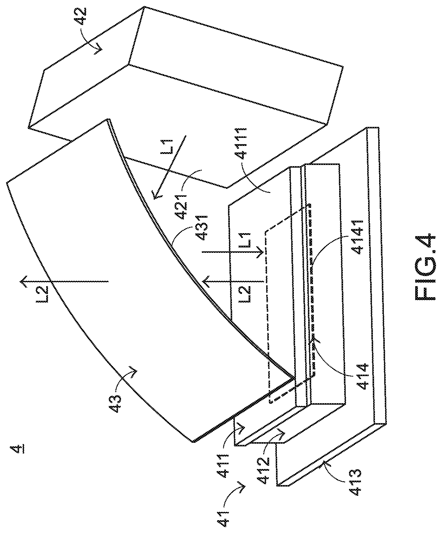
[0053] Please refer to FIGS. 4, 5 and 6. FIG. 4 is a schematic perspective view illustrating a display device according to an embodiment of the present invention. FIG. 5 schematically illustrates an imaging element of the display device as shown in FIG. 4 and the viewing angles of plural pixels on an imaging surface of the imaging element. FIG. 6 schematically illustrates the optical paths of the display device as shown in FIG. 4. The display device 4 comprises an imaging element 41, a flat surface light source 42 and a polarization beam splitter 43. The imaging element 41 has an imaging surface 414 for providing an image. The flat surface light source 42 has a light emitting surface 421 for providing plural illumination beams L1. Moreover, the normal line of the light emitting surface 421 of the flat surface light source 42 and the normal line of the imaging surface 414 of the imaging element 41 are not perpendicular to each other.
[0054] The polarization beam splitter 43 is arranged between the flat surface light source 42 and the imaging element 41. Moreover, the polarization beam splitter 43 has a geometric surface 431. When an illumination beam L1 in a first polarization state and from the flat surface light source 42 is projected on the geometric surface 431, the illumination beam L1 is reflected to the imaging element 41. When the illumination beam L1 in the first polarization state is projected on the imaging surface 414 of the imaging element 41, the illumination beam L1 is reflected as an imaging beam. After the imaging beam is exited from the imaging element 41, an imaging beam L2 in a second polarization state is generated. The imaging beam L2 in the second polarization state is directed to the polarization beam splitter 43. After the imaging beam L2 in the second polarization state is transmitted through the geometric surface 431 of the polarization beam splitter 43, the imaging beam L2 in the second polarization state is outputted.
[0055] Moreover, the illumination beam L1 in the first polarization state is projected on each pixel of the imaging surface 414 of the imaging element 41 at an incidence angle .theta..sub.i. When the illumination beam L1 in the first polarization state is projected on the imaging surface 414 of the imaging element 41, the imaging beam L2 in the second polarization state is reflected at a reflection angle .theta..sub.r. The reflection angle .theta..sub.r is equal to the incidence angle .theta..sub.i. Consequently, as shown in FIG. 5, the field of view .theta..sub.v of each pixel is determined according to the incidence angle .theta..sub.i of illumination beam L1 on the pixel.
[0056] In an embodiment, the imaging element 41 is a LCoS (liquid crystal on silicon) element. The imaging element 41 comprises a top glass cover 411, a circuit board 413 and an intermediate structure 412. The intermediate structure 412 is arranged between the top glass cover 411 and the circuit board 413. The intermediate structure 412 contains an electrode layer, a liquid crystal layer, an alignment layer, a reflective layer, a silicon crystal layer, and so on. The components of the intermediate structure 412 are well known to those skilled in the art, and are not redundantly described herein. The imaging surface 414 is disposed within the intermediate structure 412 and has a rectangular shape. In this embodiment, the polarization beam splitter 43 has a thin film structure. An example of the polarization beam splitter 43 includes but is not limited to a reflective polarizer or a dual brightness enhancement film (DBEF). The geometric surface 431 is a uniaxial curvy surface with a curvature.
[0057] Hereinafter, three examples of the flat surface light source 42 will be described.
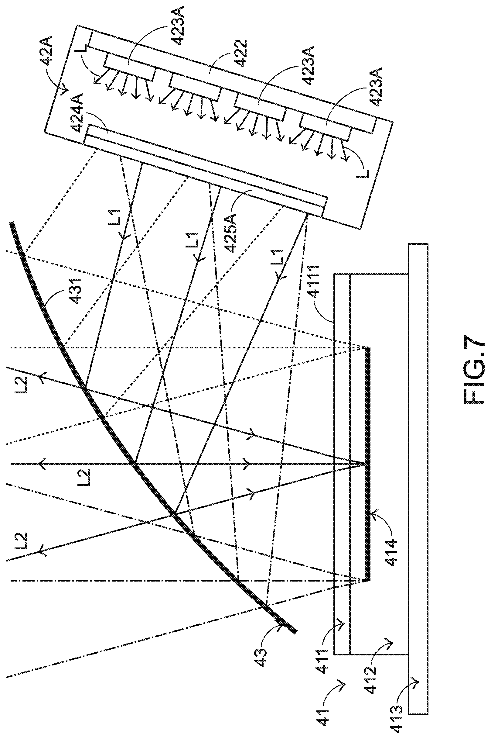
[0058] Please refer to FIGS. 7 and 8. FIG. 7 schematically illustrates a first exemplary flat surface light source used in the display device as shown in FIG. 4. FIG. 8 is a schematic perspective view illustrating a portion of the flat surface light source as shown in FIG. 7. In this embodiment, the flat surface light source 42A comprises a substrate 422, plural light emitting diodes 423A, a diffusion plate 424A and a polarizer 425A. The plural light emitting diodes 423A are arranged on the substrate 422 in a two-dimensional array. When the plural light beams L from the plural light emitting diodes 423A are projected to the diffusion plate 424A, the light beams L are scattered. After the light beams L are transmitted through the diffusion plate 424A, a uniform surface light source is generated. After the light beams L are transmitted through the polarizer 425A, the plural illumination beams L1 in the first polarization state are generated. Due to the arrangement of the polarizer 425A, portions of the light beams L passing through the diffusion plate 424A will not be directly transmitted through the polarization beam splitter 43. Consequently, the possibility of generating the stray light is reduced, and the contrast and displaying efficacy of the display device 4 are enhanced. However, the polarizer 425A is not the essential component of the flat surface light source 42A.
[0059] FIG. 9 schematically illustrates a second exemplary flat surface light source used in the display device as shown in FIG. 4. In this embodiment, the flat surface light source 42B comprises a light chamber 426, at least one light emitting diode 423B, a diffusion plate 424B and a polarizer 425B. The light emitting diode 423B is located at a first end of the light chamber 426. The diffusion plate 424B is located at a second end of the light chamber 426. The plural light beams L from the light emitting diode 423B are transferred within the light chamber 426. After the light beams L are reflected and scattered by an inner surface 4261 of the light chamber 426 many times, the light beams are projected to the diffusion plate 424B. The light beams L are also scattered within the diffusion plate 424B. After the light beams L are transmitted through the diffusion plate 424B, a uniform surface light source is generated. After the light beams L are transmitted through the polarizer 425B, the plural illumination beams L1 in the first polarization state are generated. Due to the arrangement of the polarizer 425B, portions of the light beams L passing through the diffusion plate 424B will not be directly transmitted through the polarization beam splitter 43. Consequently, the possibility of generating the stray light is reduced, and the contrast and displaying efficacy of the display device 4 are enhanced. However, the polarizer 425B is not the essential component of the flat surface light source 42B.
[0060] FIG. 10 schematically illustrates a third exemplary flat surface light source used in the display device as shown in FIG. 4. In this embodiment, the flat surface light source 42C comprises at least one light emitting diode 423C, a light guide plate 427 and a polarizer 425C. After plural light beams L from the at least one light emitting diode 423C are introduced into the light guide plate 427, the light beams L are guided by the light guide plate 427 and reflected and scattered within the light guide plate 427 many times. After the light beams L are transmitted through the light guide plate 427, a uniform surface light source is generated. After the light beams L are transmitted through the polarizer 425C, the plural illumination beams L1 in the first polarization state are generated. Due to the arrangement of the polarizer 425C, portions of the light beams L passing through the light guide plate 427 will not be directly transmitted through the polarization beam splitter 43. Consequently, the possibility of generating the stray light is reduced, and the contrast and displaying efficacy of the display device 4 are enhanced. However, the polarizer 425c is not the essential component of the flat surface light source 42C.
[0061] The above examples are presented herein for purpose of illustration and description only. The type of the imaging element, the shape of the imaging surface, the type of the polarization beam splitter, the shape of the geometric surface and the type of the flat surface light source are not restricted. It is noted that numerous modifications and alterations may be made while retaining the teachings of the invention.
[0062] Moreover, the distance between the geometric surface 431 of the polarization beam splitter 43 and the top glass cover 411 of the imaging element 41 has a specified distribution, and the flat surface light source 42 has a specified inclination angle. Consequently, the imaging surface 414 of the imaging element 41 can be irradiated uniformly by the illumination beams L1 from the flat surface light source 42 within a specified field of view .theta..sub.v. In an embodiment, the display device further comprises a light-transmissible carrier (not shown). The light-transmissible carrier has an optical curvy surface corresponding to the geometric surface 431 of the polarization beam splitter 43. Consequently, the polarization beam splitter 43 is installed on the light-transmissible carrier. Preferably but not exclusively, the light-transmissible carrier is produced by a glass grinding process or a plastic molding process.
[0063] The distance distribution between the geometric surface 431 of the polarization beam splitter 43 and the top glass cover 411 of the imaging element 41 and the relationship between the distance distribution and the inclination angle of the flat surface light source 42 will be described as follows.
[0064] FIG. 11 schematically illustrates the geometric concepts of the display device as shown in FIG. 4 according to a coordinate system. In the coordinate system of FIG. 11, a first coordinate axis (e.g., the X axis) is parallel with a side of the imaging surface 414 of the imaging element 41 and perpendicular to the normal line of the imaging surface 414. In the embodiment as shown in FIG. 4, the side of the imaging surface 414 is a short side 4141 of the imaging surface 414. The origin X.sub.0 of the first coordinate axis (e.g., the X axis) is located at a middle point of the short side 4141 of the imaging surface 414. The axial direction of the first coordinate axis (e.g., the X axis) faces the flat surface light source 42. In the coordinate system of FIG. 11, a second coordinate axis (e.g., the Y axis) is parallel with the normal line of the imaging surface 414. The origin Y.sub.0 of the second coordinate axis (e.g., the Y axis) is located at the top surface of the imaging element 41 (i.e., a top surface 4111 of the top glass cover 411). The axis direction of the second coordinate axis (e.g., the Y axis) faces the polarization beam splitter 43.
[0065] Moreover, there is an included angle .theta..sub.t between the normal line of the light emitting surface 421 of the flat surface light source 42 and the normal line of the imaging surface 414 of the imaging element 41. According to the first coordinate axis (e.g., the X axis), a position G.sub.i on the imaging surface 414 of the imaging element 41 is defined as X.sub.i. The spacing distance between the position G.sub.i of the imaging surface 414 and the geometric surface 431 of the polarization beam splitter 43 along the normal line of the imaging surface 414 is defined as M.sub.i. The spacing distance between the position G.sub.i of the imaging surface 414 and the top surface of the imaging element 41 (i.e., a top surface 4111 of the top glass cover 411) along the normal line of the imaging surface 41 is defined as N.sub.i. Moreover, a half of the length of the short side 4141 of imaging surface 414 is defined as dX.
[0066] If a half of the length of the short side 4141 (dX) is smaller than 2.75 mm, the display device 4 satisfies the following mathematic formulae (1).about.(4):
-0.047385 X.sub.i.sup.2+0.771625 X.sub.i+3.4.ltoreq.Y.sub.i; (1)
Y.sub.i.ltoreq.-0.047385 X.sub.i.sup.2+0.771625 X.sub.i+5; (2)
Y.sub.i=M.sub.i-N.sub.i; and (3)
69.degree..ltoreq..theta..sub.t.ltoreq.78.degree.. (4)
[0067] If the half of the length of the short side 4141 (dX) is larger than 2.75 mm and smaller than 3.5 mm, the display device 4 further satisfies the following mathematic formulae (5).about.(8):
-0.043299 X.sub.i.sup.2+0.745345 X.sub.i+4.ltoreq.Y.sub.i; (5)
Y.sub.i.ltoreq.-0.043299 X.sub.i.sup.2+0.745345 X.sub.i+6; (6)
Y.sub.i=M.sub.i-N.sub.i; and (7)
68.5.degree..ltoreq..theta..sub.t.ltoreq.82.5.degree.. (8)
[0068] As the position G.sub.i on the imaging surface 414 of the imaging element 41 is moved along the axis direction of the first coordinate axis (e.g., the X axis), the position G.sub.i is closer to the flat surface light source 42 and the X.sub.i is increased. That is, the spacing distance M.sub.i between the position G.sub.i of the imaging surface 414 and the geometric surface 431 of the polarization beam splitter 43 along the normal line of the imaging surface 414 is increased.
[0069] In case that the display device 4 of the present invention satisfies the above mathematic formulae, the imaging surface 414 of the imaging element 41 can be irradiated uniformly by the illumination beams L1 from the flat surface light source 42. In accordance with the present invention, the illumination uniformity on the imaging surface 414 of the imaging element 41 has a specific definition.
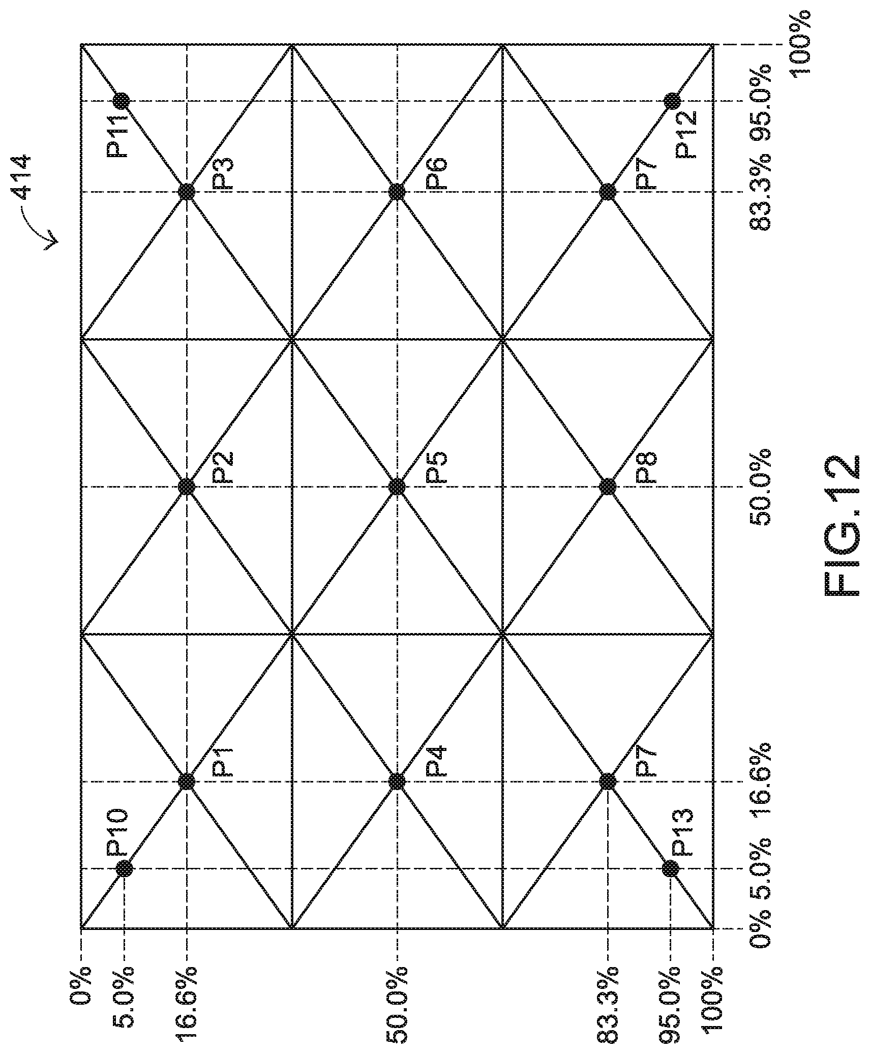
[0070] FIG. 12 schematically illustrates plural positions of the imaging surface of the imaging element for calculating the illumination uniformity and the relationship between the plural positions and the edges of the imaging surface. For example, the distance between the position P1 and the top edge of the imaging surface 414 is 16.6% of the length of the left side of the imaging surface 414, and the distance between the position P1 and left side of the imaging surface 414 is equal to 16.6% of the length of the top side of the imaging surface 414. The rest of the positions P2.about.P13 may be deduced by analogy. When the positions P1.about.P13 are irradiated by the illumination beams L1, the illumination values of the pixels on these positions within a specified field of view may be expressed as E1.about.E13. The illumination uniformity U on the imaging surface 414 of the imaging element 41 may be expressed by the following formula:
U=(E.sub.min/E.sub.max).times.100%.
[0071] In the above mathematic formula, E.sub.min is the minimum of these illumination values E1.about.E13, and E.sub.max is the maximum of these illumination values E1.about.E13.
[0072] The imaging surface 414 has a short side 4141. If a half of the length of the short side 4141 (dX) is smaller than 2.75 mm, the display device 4 further satisfies the following mathematic formulae (a1).about.(a6):
if X.sub.i=0, 3.6.ltoreq.Y.sub.i.ltoreq.3.8 (see Example 10, Example 11 and Example 12 as follows); (a1)
if X.sub.i=0, 3.8.ltoreq.Y.sub.i.ltoreq.4.0 (see Example 7, Example 8, Example 9 and Example 19 as follows); (a2)
if X.sub.i=0, 4.0.ltoreq.Y.sub.i.ltoreq.4.2 (see Example 6, Example 17, Example 18, Example 20 and Example 21 as follows); (a3)
if X.sub.i=0, 4.2.ltoreq.Y.sub.i.ltoreq.4.4 (see Example 5, Example 16, Example 23, Example 25, Example 26 and Example 27 as follows); (a4)
if X.sub.i=0, 4.4.ltoreq.Y.sub.i.ltoreq.4.6 (see Example 3, Example 4, Example 13, Example 14, Example 22 and Example 24 as follows); and (a5)
if X.sub.i=0, 4.6.ltoreq.Y.sub.i.ltoreq.4.8 (see Example 1, Example 2 and Example 15 as follows). (a6)
[0073] If the half of the length of the short side 4141 (dX) is larger than 2.75 mm and smaller than 3.5 mm, the display device 4 further satisfies the following mathematic formulae (b1).about.(b8):
if X.sub.i=0, 4.2.ltoreq.Y.sub.i.ltoreq.4.4 (see Example 38 as follows); (b1)
if X.sub.i=0, 4.4.ltoreq.Y.sub.i.ltoreq.4.6 (see Example 37, Example 39, Example 40, Example 41, Example 53 and Example 54 as follows); (b2)
if X.sub.i=0, 4.6.ltoreq.Y.sub.i.ltoreq.4.8 (see Example 34, Example 36 and Example 52 as follows); (b3)
if X.sub.i=0, 4.8.ltoreq.Y.sub.i.ltoreq.5.0 (see Example 31, Example 33, Example 35, Example 49, Example 51, Example 60, Example 61, Example 62 and Example 63 as follows); (b4)
if X.sub.i=0, 5.0.ltoreq.Y.sub.i.ltoreq.5.2 (see Example 48, Example 50, Example 57, Example 58 and Example 59 as follows); (b5)
if X.sub.i=0, 5.2.ltoreq.Y.sub.i.ltoreq.5.4 (see Example 30, Example 32, Example 43, Example 45, Example 46, Example 47, Example 55 and Example 56 as follows); (b6)
if X.sub.i=0, 5.4.ltoreq.Y.sub.i.ltoreq.5.6 (see Example 29, Example 42 and Example 44 as follows); and (b7)
if X.sub.i=0, 5.6.ltoreq.Y.sub.i.ltoreq.5.8 (see Example 28 as follows). (b8)
[0074] Hereinafter, sixty three examples obtained according to the above mathematic formula (1).about.(4) or the above mathematic formula (5).about.(8) are listed in the following tables (e.g., Table 1.about.63). In all of these embodiments, the illumination uniformity U on the imaging surface 414 of the imaging element 41 is larger than 85%.
TABLE-US-00001 TABLE 1 Example 1 dX = 2.376 mm, .theta..sub.v = 20.degree., .theta..sub.t = 76.523.degree. X.sub.i (mm) -2.376 -1.584 -0.792 0 0.792 1.584 2.376 Y.sub.i (mm) 2.713 3.444 4.136 4.792 5.415 6.005 6.565
TABLE-US-00002 TABLE 2 Example 2 dX = 2.376 mm, .theta..sub.v = 20.degree., .theta..sub.t = 75.457.degree. X.sub.i (mm) -2.376 -1.584 -0.792 0 0.792 1.584 2.376 Y.sub.i (mm) 2.657 3.391 4.080 4.726 5.333 5.903 6.438
TABLE-US-00003 TABLE 3 Example 3 dX = 2.376 mm, .theta..sub.v = 20.degree., .theta..sub.t = 76.522.degree. X.sub.i (mm) -2.376 -1.584 -0.792 0 0.792 1.584 2.376 Y.sub.i (mm) 2.406 3.164 3.871 4.530 5.146 5.722 6.261
TABLE-US-00004 TABLE 4 Example 4 dX = 2.376 mm, .theta..sub.v = 20.degree., .theta..sub.t = 72.455.degree. X.sub.i (mm) -2.376 -1.584 -0.792 0 0.792 1.584 2.376 Y.sub.i (mm) 2.590 3.311 3.977 4.592 5.161 5.687 6.173
TABLE-US-00005 TABLE 5 Example 5 dX = 2.376 mm, .theta..sub.v = 20.degree., .theta..sub.t = 73.528.degree. X.sub.i (mm) -2.376 -1.584 -0.792 0 0.792 1.584 2.376 Y.sub.i (mm) 2.335 3.078 3.760 4.388 4.966 5.499 5.989
TABLE-US-00006 TABLE 6 Example 6 dX = 2.376 mm, .theta..sub.v = 20.degree., .theta..sub.t = 75.632.degree. X.sub.i (mm) -2.376 -1.584 -0.792 0 0.792 1.584 2.376 Y.sub.i (mm) 1.991 2.768 3.479 4.132 4.731 5.281 5.787
TABLE-US-00007 TABLE 7 Example 7 dX = 2.376 mm, .theta..sub.v = 20.degree., .theta..sub.t = 76.963.degree. X.sub.i (mm) -2.376 -1.584 -0.792 0 0.792 1.584 2.376 Y.sub.i (mm) 1.713 2.517 3.250 3.918 4.529 5.089 5.601
TABLE-US-00008 TABLE 8 Example 8 dX = 2.376 mm, .theta..sub.v = 20.degree., .theta..sub.t = 75.568.degree. X.sub.i (mm) -2.376 -1.584 -0.792 0 0.792 1.584 2.376 Y.sub.i (mm) 1.671 2.472 3.195 3.848 4.440 4.977 5.463
TABLE-US-00009 TABLE 9 Example 9 dX = 2.376 mm, .theta..sub.v = 20.degree., .theta..sub.t = 72.072.degree. X.sub.i (mm) -2.376 -1.584 -0.792 0 0.792 1.584 2.376 Y.sub.i (mm) 1.795 2.571 3.262 3.877 4.427 4.919 5.356
TABLE-US-00010 TABLE 10 Example 10 dX = 2.376 mm, .theta..sub.v = 20.degree., .theta..sub.t = 73.248.degree. X.sub.i (mm) -2.376 -1.584 -0.792 0 0.792 1.584 2.376 Y.sub.i (mm) 1.533 2.335 3.044 3.674 4.233 4.730 5.171
TABLE-US-00011 TABLE 11 Example 11 dX = 2.376 mm, .theta..sub.v = 20.degree., .theta..sub.t = 72.05.degree. X.sub.i (mm) -2.376 -1.584 -0.792 0 0.792 1.584 2.376 Y.sub.i (mm) 1.494 2.294 2.995 3.611 4.154 4.632 5.051
TABLE-US-00012 TABLE 12 Example 12 dX = 2.376 mm, .theta..sub.v = 20.degree., .theta..sub.t = 69.62.degree. X.sub.i (mm) -2.376 -1.584 -0.792 0 0.792 1.584 2.376 Y.sub.i (mm) 1.561 2.426 3.138 3.731 4.226 4.637 4.972
TABLE-US-00013 TABLE 13 Example 13 dX = 2.376 mm, .theta..sub.v = 30.degree., .theta..sub.t = 77.166.degree. X.sub.i (mm) -2.376 -1.584 -0.792 0 0.792 1.584 2.376 Y.sub.i (mm) 2.351 3.166 3.907 4.586 5.206 5.775 6.296
TABLE-US-00014 TABLE 14 Example 14 dX = 2.376 mm, .theta..sub.v = 30.degree., .theta..sub.t = 76.335.degree. X.sub.i (mm) -2.376 -1.584 -0.792 0 0.792 1.584 2.376 Y.sub.i (mm) 2.286 3.102 3.838 4.508 5.116 5.670 6.175
TABLE-US-00015 TABLE 15 Example 15 dX = 2.376 mm, .theta..sub.v = 30.degree., .theta..sub.t = 72.565.degree. X.sub.i (mm) -2.376 -1.584 -0.792 0 0.792 1.584 2.376 Y.sub.i (mm) 2.496 3.277 3.975 4.603 5.168 5.676 6.132
TABLE-US-00016 TABLE 16 Example 16 dX = 2.376 mm, .theta..sub.v = 30.degree., .theta..sub.t = 74.781.degree. X.sub.i (mm) -2.376 -1.584 -0.792 0 0.792 1.584 2.376 Y.sub.i (mm) 2.137 2.955 3.684 4.337 4.923 5.450 5.922
TABLE-US-00017 TABLE 17 Example 17 dX = 2.376 mm, .theta..sub.v = 30.degree., .theta..sub.t = 75.563.degree. X.sub.i (mm) -2.376 -1.584 -0.792 0 0.792 1.584 2.376 Y.sub.i (mm) 1.914 2.751 3.495 4.157 4.749 5.278 5.751
TABLE-US-00018 TABLE 18 Example 18 dX = 2.376 mm, .theta..sub.v = 30.degree., .theta..sub.t = 72.973.degree. X.sub.i (mm) -2.376 -1.584 -0.792 0 0.792 1.584 2.376 Y.sub.i (mm) 2.000 2.817 3.535 4.169 4.731 5.227 5.665
TABLE-US-00019 TABLE 19 Example 19 dX = 2.376 mm, .theta..sub.v = 30.degree., .theta..sub.t = 74.332.degree. X.sub.i (mm) -2.376 -1.584 -0.792 0 0.792 1.584 2.376 Y.sub.i (mm) 1.728 2.573 3.312 3.961 4.534 5.038 5.482
TABLE-US-00020 TABLE 20 Example 20 dX = 2.376 mm, .theta..sub.v = 30.degree., .theta..sub.t = 72.912.degree. X.sub.i (mm) -2.376 -1.584 -0.792 0 0.792 1.584 2.376 Y.sub.i (mm) 1.771 2.659 3.407 4.044 4.588 5.052 5.445
TABLE-US-00021 TABLE 21 Example 21 dX = 2.376 mm, .theta..sub.v = 30.degree., .theta..sub.t = 71.674.degree. X.sub.i (mm) -2.376 -1.584 -0.792 0 0.792 1.584 2.376 Y.sub.i (mm) 1.833 2.799 3.568 4.193 4.703 5.118 5.449
TABLE-US-00022 TABLE 22 Example 22 dX = 2.376 mm, .theta..sub.v = 38.degree., .theta..sub.t = 75.678.degree. X.sub.i (mm) -2.376 -1.584 -0.792 0 0.792 1.584 2.376 Y.sub.i (mm) 2.307 3.159 3.915 4.589 5.191 5.730 6.211
TABLE-US-00023 TABLE 23 Example 23 dX = 2.376 mm, .theta..sub.v = 38.degree., .theta..sub.t = 76.774.degree. X.sub.i (mm) -2.376 -1.584 -0.792 0 0.792 1.584 2.376 Y.sub.i (mm) 2.058 2.935 3.709 4.395 5.006 5.551 6.036
TABLE-US-00024 TABLE 24 Example 24 dX = 2.376 mm, .theta..sub.v = 38.degree., .theta..sub.t = 72.834.degree. X.sub.i (mm) -2.376 -1.584 -0.792 0 0.792 1.584 2.376 Y.sub.i (mm) 2.306 3.142 3.873 4.515 5.082 5.581 6.021
TABLE-US-00025 TABLE 25 Example 25 dX = 2.376 mm, .theta..sub.v = 38.degree., .theta..sub.t = 72.889.degree. X.sub.i (mm) -2.376 -1.584 -0.792 0 0.792 1.584 2.376 Y.sub.i (mm) 2.155 3.002 3.738 4.381 4.946 5.441 5.874
TABLE-US-00026 TABLE 26 Example 26 dX = 2.376 mm, .theta..sub.v = 38.degree., .theta..sub.t = 73.436.degree. X.sub.i (mm) -2.376 -1.584 -0.792 0 0.792 1.584 2.376 Y.sub.i (mm) 1.957 2.821 3.568 4.218 4.785 5.281 5.711
TABLE-US-00027 TABLE 27 Example 27 dX = 2.376 mm, .theta..sub.v = 38.degree., .theta..sub.t = 72.664.degree. X.sub.i (mm) -2.376 -1.584 -0.792 0 0.792 1.584 2.376 Y.sub.i (mm) 1.944 2.840 3.595 4.239 4.789 5.260 5.660
TABLE-US-00028 TABLE 28 Example 28 dX = 3.096 mm, .theta..sub.v = 20.degree., .theta..sub.t = 75.41.degree. X.sub.i (mm) -3.096 -2.064 -1.032 0 1.032 2.064 3.096 Y.sub.i (mm) 3.035 3.980 4.861 5.685 6.455 7.175 7.848
TABLE-US-00029 TABLE 29 Example 29 dX = 3.096 mm, .theta..sub.v = 20.degree., .theta..sub.t = 76.553.degree. X.sub.i (mm) -3.096 -2.064 -1.032 0 1.032 2.064 3.096 Y.sub.i (mm) 2.767 3.732 4.632 5.472 6.258 6.992 7.679
TABLE-US-00030 TABLE 30 Example 30 dX = 3.096 mm, .theta..sub.v = 20.degree., .theta..sub.t = 77.947.degree. X.sub.i (mm) -3.096 -2.064 -1.032 0 1.032 2.064 3.096 Y.sub.i (mm) 2.441 3.432 4.355 5.216 6.021 6.773 7.476
TABLE-US-00031 TABLE 31 Example 31 dX = 3.096 mm, .theta..sub.v = 20.degree., .theta..sub.t = 79.352.degree. X.sub.i (mm) -3.096 -2.064 -1.032 0 1.032 2.064 3.096 Y.sub.i (mm) 2.113 3.131 4.078 4.961 5.785 6.555 7.275
TABLE-US-00032 TABLE 32 Example 32 dX = 3.096 mm, .theta..sub.v = 20.degree., .theta..sub.t = 73.604.degree. X.sub.i (mm) -3.096 -2.064 -1.032 0 1.032 2.064 3.096 Y.sub.i (mm) 2.589 3.538 4.409 5.210 5.946 6.625 7.249
TABLE-US-00033 TABLE 33 Example 33 dX = 3.096 mm, .theta..sub.v = 20.degree., .theta..sub.t = 74.657.degree. X.sub.i (mm) -3.096 -2.064 -1.032 0 1.032 2.064 3.096 Y.sub.i (mm) 2.315 3.291 4.182 4.999 5.748 6.435 7.064
TABLE-US-00034 TABLE 34 Example 34 dX = 3.096 mm, .theta..sub.v = 20.degree., .theta..sub.t = 75.71.degree. X.sub.i (mm) -3.096 -2.064 -1.032 0 1.032 2.064 3.096 Y.sub.i (mm) 2.040 3.044 3.958 4.791 5.551 6.246 6.880
TABLE-US-00035 TABLE 35 Example 35 dX = 3.096 mm, .theta..sub.v = 20.degree., .theta..sub.t = 71.782.degree. X.sub.i (mm) -3.096 -2.064 -1.032 0 1.032 2.064 3.096 Y.sub.i (mm) 2.287 3.250 4.115 4.894 5.596 6.228 6.796
TABLE-US-00036 TABLE 36 Example 36 dX = 3.096 mm, .theta..sub.v = 20.degree., .theta.0.sub.t = 71.607.degree. X.sub.i (mm) -3.096 -2.064 -1.032 0 1.032 2.064 3.096 Y.sub.i (mm) 2.139 3.113 3.982 4.759 5.456 6.078 6.634
TABLE-US-00037 TABLE 37 Example 37 dX = 3.096 mm, .theta..sub.v = 20.degree., .theta..sub.t = 72.355.degree. X.sub.i (mm) -3.096 -2.064 -1.032 0 1.032 2.064 3.096 Y.sub.i (mm) 1.897 2.896 3.782 4.570 5.273 5.899 6.454
TABLE-US-00038 TABLE 38 Example 38 dX = 3.096 mm, .theta..sub.v = 20.degree., .theta..sub.t = 73.381.degree. X.sub.i (mm) -3.096 -2.064 -1.032 0 1.032 2.064 3.096 Y.sub.i (mm) 1.627 2.655 3.563 4.366 5.079 5.711 6.270
TABLE-US-00039 TABLE 39 Example 39 dX = 3.096 mm, .theta..sub.v = 20.degree., .theta..sub.t = 73.012.degree. X.sub.i (mm) -3.096 -2.064 -1.032 0 1.032 2.064 3.096 Y.sub.i (mm) 1.562 2.668 3.605 4.405 5.092 5.679 6.179
TABLE-US-00040 TABLE 40 Example 40 dX = 3.096 mm, .theta..sub.v = 20.degree., .theta..sub.t = 71.435.degree. X.sub.i (mm) -3.096 -2.064 -1.032 0 1.032 2.064 3.096 Y.sub.i (mm) 1.571 2.696 3.627 4.406 5.061 5.608 6.061
TABLE-US-00041 TABLE 41 Example 41 dX = 3.096 mm, .theta..sub.v = 20.degree., .theta..sub.t = 70.667.degree. X.sub.i (mm) -3.096 -2.064 -1.032 0 1.032 2.064 3.096 Y.sub.i (mm) 1.576 2.714 3.643 4.412 5.050 5.576 6.004
TABLE-US-00042 TABLE 42 Example 42 dX = 3.096 mm, .theta..sub.v = 30.degree., .theta..sub.t = 78.871.degree. X.sub.i (mm) -3.096 -2.064 -1.032 0 1.032 2.064 3.096 Y.sub.i (mm) 2.562 3.618 4.584 5.472 6.289 7.041 7.734
TABLE-US-00043 TABLE 43 Example 43 dX = 3.096 mm, .theta..sub.v = 30.degree., .theta..sub.t = 78.358.degree. X.sub.i (mm) -3.096 -2.064 -1.032 0 1.032 2.064 3.096 Y.sub.i (mm) 2.484 3.543 4.506 5.388 6.194 6.933 7.611
TABLE-US-00044 TABLE 44 Example 44 dX = 3.096 mm, .theta..sub.v = 30.degree., .theta..sub.t = 76.531.degree. X.sub.i (mm) -3.096 -2.064 -1.032 0 1.032 2.064 3.096 Y.sub.i (mm) 2.565 3.605 4.546 5.400 6.178 6.885 7.530
TABLE-US-00045 TABLE 45 Example 45 dX = 3.096 mm, .theta..sub.v = 30.degree., .theta..sub.t = 77.424.degree. X.sub.i (mm) -3.096 -2.064 -1.032 0 1.032 2.064 3.096 Y.sub.i (mm) 2.311 3.377 4.337 5.206 5.993 6.707 7.355
TABLE-US-00046 TABLE 46 Example 46 dX = 3.096 mm, .theta..sub.v = 30.degree., .theta..sub.t = 74.727.degree. X.sub.i (mm) -3.096 -2.064 -1.032 0 1.032 2.064 3.096 Y.sub.i (mm) 2.487 3.521 4.445 5.275 6.021 6.692 7.295
TABLE-US-00047 TABLE 47 Example 47 dX = 3.096 mm, .theta..sub.v = 30.degree., .theta..sub.t = 72.502.degree. X.sub.i (mm) -3.096 -2.064 -1.032 0 1.032 2.064 3.096 Y.sub.i (mm) 2.594 3.605 4.502 5.301 6.014 6.649 7.215
TABLE-US-00048 TABLE 48 Example 48 dX = 3.096 mm, .theta..sub.v = 30.degree., .theta..sub.t = 73.361 X.sub.i (mm) -3.096 -2.064 -1.032 0 1.032 2.064 3.096 Y.sub.i (mm) 2.345 3.381 4.296 5.107 5.829 6.469 7.037
TABLE-US-00049 TABLE 49 Example 49 dX = 3.096 mm, .theta..sub.v = 30.degree., .theta..sub.t = 74.234.degree. X.sub.i (mm) -3.096 -2.064 -1.032 0 1.032 2.064 3.096 Y.sub.i (mm) 2.094 3.156 4.090 4.914 5.644 6.290 6.861
TABLE-US-00050 TABLE 50 Example 50 dX = 3.096 mm, .theta..sub.v = 30.degree., .theta..sub.t = 68.904.degree. X.sub.i (mm) -3.096 -2.064 -1.032 0 1.032 2.064 3.096 Y.sub.i (mm) 2.528 3.520 4.382 5.133 5.789 6.361 6.855
TABLE-US-00051 TABLE 51 Example 51 dX = 3.096 mm, .theta..sub.v = 30.degree., .theta..sub.t = 70.186.degree. X.sub.i (mm) -3.096 -2.064 -1.032 0 1.032 2.064 3.096 Y.sub.i (mm) 2.233 3.258 4.143 4.913 5.582 6.163 6.664
TABLE-US-00052 TABLE 52 Example 52 dX = 3.096 mm, .theta..sub.v = 30.degree., .theta..sub.t = 71.485.degree. X.sub.i (mm) -3.096 -2.064 -1.032 0 1.032 2.064 3.096 Y.sub.i (mm) 1.938 2.996 3.906 4.693 5.375 5.966 6.474
TABLE-US-00053 TABLE 53 Example 53 dX = 3.096 mm, .theta..sub.v = 30.degree., .theta..sub.t = 71.953.degree. X.sub.i (mm) -3.096 -2.064 -1.032 0 1.032 2.064 3.096 Y.sub.i (mm) 1.745 2.834 3.761 4.555 5.237 5.823 6.322
TABLE-US-00054 TABLE 54 Example 54 dX = 3.096 mm, .theta..sub.v = 30.degree., .theta..sub.t = 71.291.degree. X.sub.i (mm) -3.096 -2.064 -1.032 0 1.032 2.064 3.096 Y.sub.i (mm) 1.754 2.851 3.776 4.561 5.230 5.799 6.278
TABLE-US-00055 TABLE 55 Example 55 dX = 3.096 mm, .theta..sub.v = 38.degree., .theta..sub.t = 82.045.degree. X.sub.i (mm) -3.096 -2.064 -1.032 0 1.032 2.064 3.096 Y.sub.i (mm) 1.963 3.192 4.272 5.229 6.081 6.843 7.523
TABLE-US-00056 TABLE 56 Example 56 dX = 3.096 mm, .theta..sub.v = 38.degree., .theta..sub.t = 81.164.degree. X.sub.i (mm) -3.096 -2.064 -1.032 0 1.032 2.064 3.096 Y.sub.i (mm) 1.966 3.195 4.269 5.212 6.047 6.787 7.444
TABLE-US-00057 TABLE 57 Example 57 dX = 3.096 mm, .theta..sub.v = 38.degree., .theta..sub.t = 80.236.degree. X.sub.i (mm) -3.096 -2.064 -1.032 0 1.032 2.064 3.096 Y.sub.i (mm) 1.962 3.188 4.252 5.181 5.998 6.718 7.354
TABLE-US-00058 TABLE 58 Example 58 dX = 3.096 mm, .theta..sub.v = 38.degree., .theta..sub.t = 79.321.degree. X.sub.i (mm) -3.096 -2.064 -1.032 0 1.032 2.064 3.096 Y.sub.i (mm) 1.968 3.200 4.258 5.173 5.971 6.669 7.278
TABLE-US-00059 TABLE 59 Example 59 dX = 3.096 mm, .theta..sub.v = 38.degree., .theta..sub.t = 76.863.degree. X.sub.i (mm) -3.096 -2.064 -1.032 0 1.032 2.064 3.096 Y.sub.i (mm) 2.025 3.170 4.168 5.043 5.815 6.495 7.095
TABLE-US-00060 TABLE 60 Example 60 dX = 3.096 mm, .theta..sub.v = 38.degree., .theta..sub.t = 75.87.degree. X.sub.i (mm) -3.096 -2.064 -1.032 0 1.032 2.064 3.096 Y.sub.i (mm) 2.009 3.147 4.134 4.994 5.749 6.410 6.989
TABLE-US-00061 TABLE 61 Example 61 dX = 3.096 mm, .theta..sub.v = 38.degree., .theta..sub.t = 75.06.degree. X.sub.i (mm) -3.096 -2.064 -1.032 0 1.032 2.064 3.096 Y.sub.i (mm) 1.964 3.101 4.080 4.929 5.669 6.315 6.876
TABLE-US-00062 TABLE 62 Example 62 dX = 3.096 mm, .theta..sub.v = 38.degree., .theta..sub.t = 73.886.degree. X.sub.i (mm) -3.096 -2.064 -1.032 0 1.032 2.064 3.096 Y.sub.i (mm) 2.005 3.160 4.136 4.970 5.686 6.301 6.826
TABLE-US-00063 TABLE 63 Example 63 dX = 3.096 mm, .theta..sub.v = 38.degree., .theta..sub.t = 73.33.degree. X.sub.i (mm) -3.096 -2.064 -1.032 0 1.032 2.064 3.096 Y.sub.i (mm) 1.984 3.177 4.164 4.992 5.690 6.278 6.770
[0075] From the above descriptions, the present invention provides the display device. The distance between the geometric surface of the polarization beam splitter and the top glass cover of the imaging element has a specified distribution, and the flat surface light source has a specified inclination angle. Consequently, the imaging surface of the imaging element can be irradiated uniformly by the illumination beams from the flat surface light source within a specified viewing angle. Moreover, since the distance between the imaging element and the polarization beam splitter is shortened, the overall thickness and volume of the display device are reduced. It is not necessary to use the injection molding process or the grinding process of forming the precise optical element to produce the polarization beam splitter of the present invention. In addition, the display device is not equipped with additional precise optical elements. Consequently, the process of producing the components of the display device is simplified, and the display device is cost-effective. In other words, the display device is industrially valuable.
[0076] While the invention has been described in terms of what is presently considered to be the most practical and preferred embodiments, it is to be understood that the invention needs not be limited to the disclosed embodiments. On the contrary, it is intended to cover various modifications and similar arrangements included within the spirit and scope of the appended claims which are to be accorded with the broadest interpretation so as to encompass all modifications and similar structures.
* * * * *
D00000
D00001
D00002
D00003
D00004
D00005
D00006
D00007
D00008
D00009
D00010
D00011
D00012
XML
uspto.report is an independent third-party trademark research tool that is not affiliated, endorsed, or sponsored by the United States Patent and Trademark Office (USPTO) or any other governmental organization. The information provided by uspto.report is based on publicly available data at the time of writing and is intended for informational purposes only.
While we strive to provide accurate and up-to-date information, we do not guarantee the accuracy, completeness, reliability, or suitability of the information displayed on this site. The use of this site is at your own risk. Any reliance you place on such information is therefore strictly at your own risk.
All official trademark data, including owner information, should be verified by visiting the official USPTO website at www.uspto.gov. This site is not intended to replace professional legal advice and should not be used as a substitute for consulting with a legal professional who is knowledgeable about trademark law.