Distributed Travelling-wave Mach-zehnder Modulator Driver
Ding; Ran ; et al.
U.S. patent application number 16/699082 was filed with the patent office on 2020-06-11 for distributed travelling-wave mach-zehnder modulator driver. The applicant listed for this patent is Elenion Technologies, LLC. Invention is credited to Thomas Wetteland Baehr-Jones, Ran Ding, Michael J. Hochberg, Alexander Rylyakov.
| Application Number | 20200186253 16/699082 |
| Document ID | / |
| Family ID | 53775903 |
| Filed Date | 2020-06-11 |


| United States Patent Application | 20200186253 |
| Kind Code | A1 |
| Ding; Ran ; et al. | June 11, 2020 |
DISTRIBUTED TRAVELLING-WAVE MACH-ZEHNDER MODULATOR DRIVER
Abstract
A distributed traveling-wave Mach-Zehnder modulator driver having a plurality of modulation stages that operate cooperatively (in-phase) to provide a signal suitable for use in a 100 Gb/s optical fiber transmitter at power levels that are compatible with conventional semiconductor devices and conventional semiconductor processing is described.
| Inventors: | Ding; Ran; (New York, NY) ; Baehr-Jones; Thomas Wetteland; (Arcadia, CA) ; Hochberg; Michael J.; (New York, NY) ; Rylyakov; Alexander; (Staten Island, NY) | ||||||||||
| Applicant: |
|
||||||||||
|---|---|---|---|---|---|---|---|---|---|---|---|
| Family ID: | 53775903 | ||||||||||
| Appl. No.: | 16/699082 | ||||||||||
| Filed: | November 28, 2019 |
Related U.S. Patent Documents
| Application Number | Filing Date | Patent Number | ||
|---|---|---|---|---|
| 16398422 | Apr 30, 2019 | 10530487 | ||
| 16699082 | ||||
| 16220203 | Dec 14, 2018 | 10320488 | ||
| 16398422 | ||||
| 16108857 | Aug 22, 2018 | 10205531 | ||
| 16220203 | ||||
| 15830351 | Dec 4, 2017 | 10084545 | ||
| 16108857 | ||||
| 15234359 | Aug 11, 2016 | 9853738 | ||
| 15830351 | ||||
| 14618989 | Feb 10, 2015 | 9559779 | ||
| 15234359 | ||||
| 61937683 | Feb 10, 2014 | |||
| Current U.S. Class: | 1/1 |
| Current CPC Class: | G02F 1/025 20130101; G02F 2201/127 20130101; H04B 10/505 20130101; H04B 10/541 20130101; G02F 1/2257 20130101; G02F 2001/212 20130101; G02F 1/0123 20130101; H04B 10/5161 20130101; H04B 10/5561 20130101 |
| International Class: | H04B 10/556 20060101 H04B010/556; H04B 10/54 20060101 H04B010/54; H04B 10/516 20060101 H04B010/516; G02F 1/025 20060101 G02F001/025; G02F 1/01 20060101 G02F001/01; H04B 10/50 20060101 H04B010/50; G02F 1/225 20060101 G02F001/225 |
Claims
1-19. (canceled)
20. A modulator, comprising: an optical input waveguide for receiving an input optical signal and splitting the input optical signal into a first portion and a second portion; a plurality of sequential modulators connected to the optical input waveguide for receiving the first portion and the second portion; an optical output port for recombining the first portion and the second portion into a modulated output optical signal; a differential electrical data input connected to a data source; a plurality of driver-amplifier stages, each including a respective differential driver amplifier input, a respective differential driver amplifier output, and a respective differential signal output connected to a respective one of the sequential modulators, the respective differential driver amplifier input of a first of the plurality of driver-amplifier stages connected to the differential electrical data input; and a plurality of delay/relay stages, each including a respective differential delay/relay input connected to the respective differential driver amplifier output of a previous one of the plurality of driver-amplifier stages, and a differential delay/relay output connected to the respective differential driver amplifier input of a following one of the plurality of driver-amplifier stages; wherein an optical delay of each of the plurality of sequential modulators plus optical waveguide wiring matches a delay between the driver-amplifier stages so that modulations constructively add.
21. The modulator according to claim 20, wherein each respective differential signal output is configured to comprise an open-collector driver for driving sequential modulators with different impedances.
22. The modulator according to claim 20, wherein each respective differential signal output is configured to comprise an open-collector cascode driver for driving the sequential modulators with different impedances.
23. The modulator according to claim 22, wherein each respective differential signal output is configured to comprise an open-collector driver for driving the sequential modulators with both 25.OMEGA. and 50.OMEGA. impedances.
24. The modulator according to claim 20, further comprising: a plurality of DC bias structures, each DC bias structure configured to individually control one of said plurality of delay/relay stages; wherein each DC bias structures is configured to control an on state and an off state of a respective delay/relay stage for shutting down individual delay/relay stages.
25. The modulator according to claim 24, wherein the DC bias structures are also configured to control on and off states of a respective on of the plurality of driver-amplifier stages for shutting down individual driver amplifier stages.
26. The modulator according to claim 24, wherein each DC bias structures is also configured to control variation in biasing voltages of a respective one of the driver-amplifier stages.
27. The modulator according to claim 20, further comprising: a plurality of DC bias structures, each DC bias structure configured to individually control one of the plurality of driver amplifier stages; wherein each DC bias structures is configured to control an on state and an off state of a respective one of the driver-amplifier stages for shutting down individual driver amplifier stages.
28. The modulator according to claim 27, further comprising: wherein each DC bias structures is also configured to control variation in biasing voltages of a respective one of the driver-amplifier stages.
29. The modulator according to claim 20, further comprising: a plurality of DC bias structures, each DC bias structure configured to individually control one of the plurality of driver amplifier stages; wherein each DC bias structures is configured to control variation in biasing voltages of a respective one of the driver-amplifier stages.
30. The modulator according to claim 20, wherein each one of the driver-amplifier stages includes only a single type of transistor to enable high-speed operation.
31. The modulator according to claim 20, wherein each one of the plurality of driver amplifier stages includes a pre-amplifier stage.
32. The modulator according to claim 20, wherein the plurality of sequential modulators comprise a plurality of optical phase-shifter pairs connected in series.
33. The modulator according to claim 32, wherein each one of the plurality of phase-shifter pairs comprises a fixed optical length.
34. The modulator according to claim 32, wherein each one of the plurality of optical phase shifter pairs comprises a Mach-Zehnder interferometer modulator.
35. The modulator according to claim 20, wherein each of the first portion and the second portion comprise equal intensities.
36. The modulator according to claim 20, wherein the plurality of driver amplifier stages comprises four, and the plurality of delay/relay stages comprises three.
37. The modulator according to claim 20, wherein each one of the plurality of driver amplifier stages includes: a first pair of emitter followers including termination resistors connected to the respective differential driver amplifier input; a pre-amplifier comprising a differential pair; a buffer comprising a second pair of emitter followers; and means for splitting a differential input signal into first and second differential output signals for output the respective differential driver amplifier output, and the respective differential signal output, respectively.
38. The modulator according to claim 20, wherein the plurality of sequential modulators, the optical input waveguide, and the optical output port are integrated on a semiconductor chip; and wherein the differential electrical data input, the plurality of driver amplifier stages, and the plurality of delay/relay stages comprise drive circuitry attached to the semiconductor chip.
39. The modulator according to claim 38, further comprising flip-chip bump bonding for attaching the drive circuitry to the semiconductor chip.
Description
CROSS-REFERENCE TO RELATED APPLICATIONS
[0001] This application claims priority to and the benefit of co-pending U.S. patent application Ser. No. 16/398,422, filed Apr. 30, 2019, now allowed, which claims priority to and benefit of U.S. patent application Ser. No. 16/220,203, filed Dec. 14, 2018, now U.S. Pat. No. 10,320,488, which claims priority to co-pending U.S. patent application Ser. No. 16/108,857, filed Aug. 22, 2018, now U.S. Pat. No. 10,205,531 which claims priority to and benefit of co-pending U.S. patent application Ser. No. 15/830,351, filed Dec. 4, 2017, now U.S. Pat. No. 10,084,545, which claims priority from U.S. patent application Ser. No. 15/234,359, filed Aug. 11, 2016, now U.S. Pat. No. 9,853,738, which is a continuation-in-part of and claims priority from U.S. patent application Ser. No. 14/618,989, filed Feb. 10, 2015, issued as U.S. Pat. No. 9,559,779, which claims priority to U.S. Provisional Application No. 61/937,683 filed Feb. 10, 2014, each of which is hereby incorporated by reference herein in its entirety.
FIELD OF THE INVENTION
[0002] The invention relates to optical transmitters in general, and particularly to an optical driver for a Gigabit/second transmitter.
BACKGROUND OF THE INVENTION
[0003] Optical interconnects offer promising solutions to data transmission bottlenecks in supercomputers and in data-centers as well as other applications. Adopting higher channel data rates can greatly reduce the complexity in optical communication systems and/or further improve interconnect capacity and density.
[0004] The most important requirement on the driver amplifier is the output voltage swing. The state-of-the-art driver amplifier in CMOS/BiCMOS can output 3 Vpp at 40 Gb/s, consuming 1.35 W DC power. See for example, C. Knochenhauer, J. Scheytt, and F. Ellinger, "A Compact, Low-Power 40-GBit/s Modulator Driver With 6-V Differential Output Swing in 0.25 um SiGe BiCMOS," Solid-State Circuits, IEEE Journal of, vol. 46, no. 5, pp. 1137-1146, 2011.
[0005] At higher data rates it is difficult to maintain or improve the available drive voltage without substantial advances in the fabrication process. This trend is at odds with the increasingly higher drive voltage required by modulators at higher speed.
[0006] There is a need for improved drivers for use in optical data handling systems.
SUMMARY OF THE INVENTION
[0007] Accordingly, the present disclosure relates to a modulator, comprising: an optical input waveguide for receiving an input optical signal and splitting the input optical signal into a first portion and a second portion; a plurality of sequential modulators connected to the optical input waveguide for receiving the first portion and the second portion; an optical output port for recombining the first portion and the second portion into a modulated output optical signal; a differential electrical data input connected to a data source; a plurality of driver-amplifier stages, each including a respective differential driver amplifier input, a respective differential driver amplifier output, and a respective differential signal output connected to a respective one of the sequential modulators, the respective differential driver amplifier input of a first of the plurality of driver-amplifier stages connected to the differential electrical data input; and a plurality of delay/relay stages, each including a respective differential delay/relay input connected to the respective differential driver amplifier output of a previous one of the plurality of driver-amplifier stages, and a differential delay/relay output connected to the respective differential driver amplifier input of a following one of the plurality of driver-amplifier stages.
[0008] An optical delay of each of the plurality of sequential modulators along with optical waveguide wiring therebetween matches a delay between the driver amplifier stages so that modulations constructively add.
[0009] The foregoing and other objects, aspects, features, and advantages of the invention will become more apparent from the following description and from the claims.
BRIEF DESCRIPTION OF THE DRAWINGS
[0010] The objects and features of the invention can be better understood with reference to the drawings described below, and the claims. The drawings are not necessarily to scale, emphasis instead generally being placed upon illustrating the principles of the invention. In the drawings, like numerals are used to indicate like parts throughout the various views.
[0011] FIG. 1A is a block diagram of a typical optical transmitter and receiver of the prior art.
[0012] FIG. 1B is a graph that illustrates the power scaling versus data rate for prior art silicon traveling-wave modulators.
[0013] FIG. 2A is a circuit block diagram of a distributed traveling-wave Mach-Zehnder (TWMZ) modulator driver that operates according to principles of the invention.
[0014] FIG. 2B is a schematic circuit diagram of a driver amplifier stage of the distributed traveling-wave Mach-Zehnder modulator driver of FIG. 2A.
[0015] FIG. 2C is a schematic circuit diagram of a delay/relay stage of the distributed traveling-wave Mach-Zehnder modulator driver of FIG. 2A.
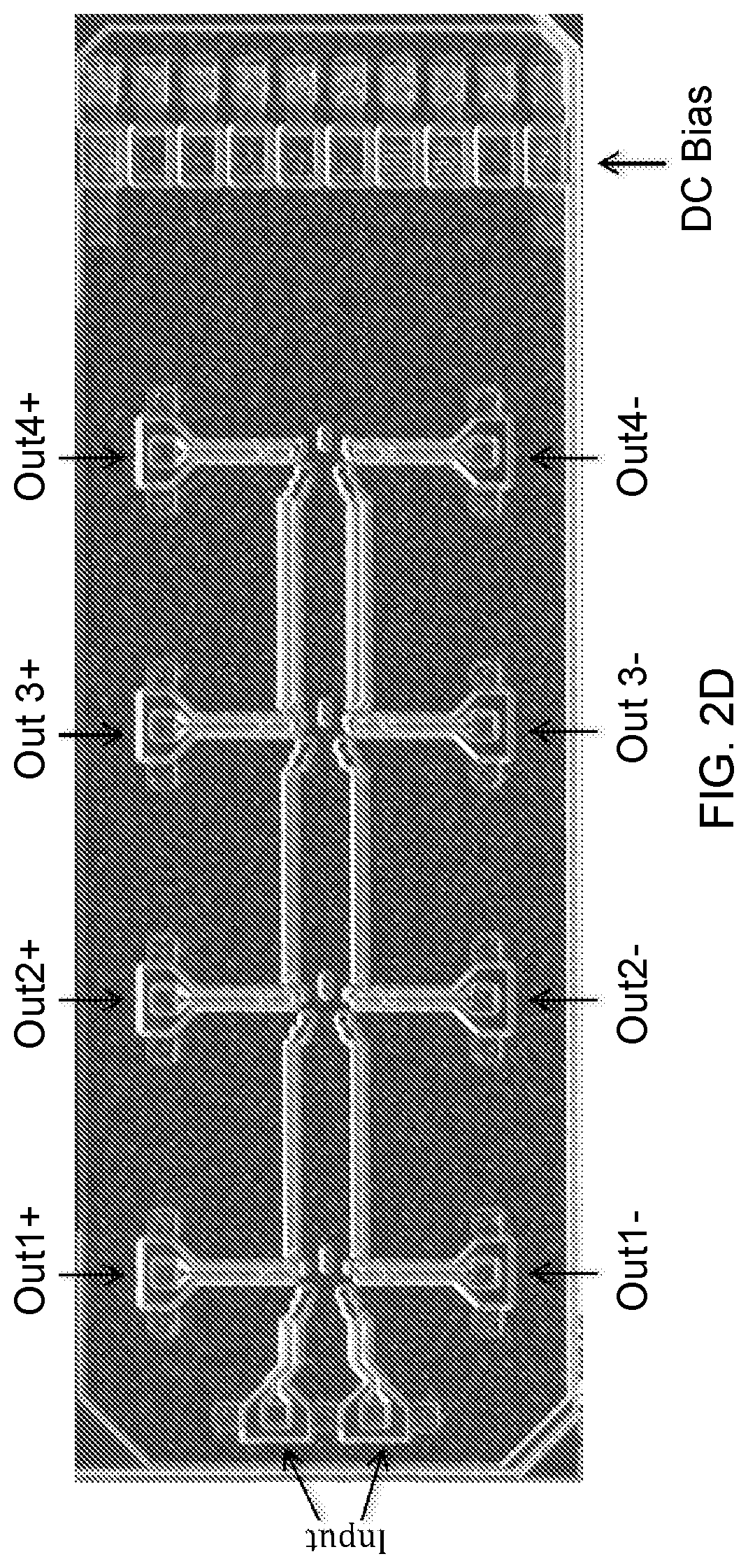
[0016] FIG. 2D is an image of a chip that embodies the distributed traveling-wave Mach-Zehnder modulator driver of FIG. 2A. The chip has a width of 1 mm and a length of 2.9 mm. DC bias is provided by the structure at the right side of the chip.
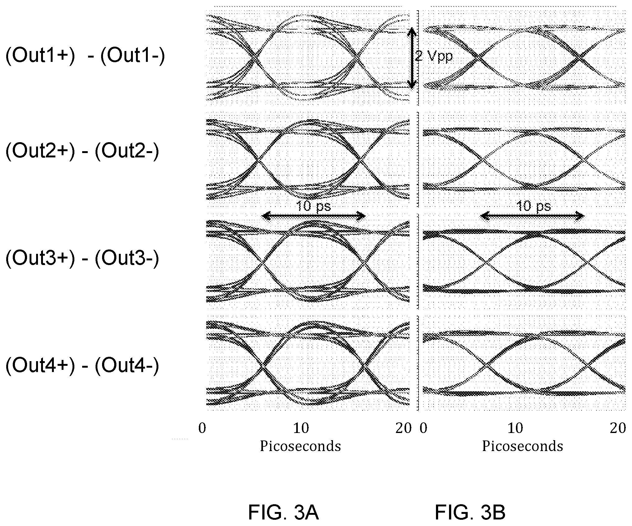
[0017] FIG. 3A is a graph that illustrates the results of a distributed TWMZ driver post-layout simulation showing 100 Gb/s eye-diagrams at the driver outputs.
[0018] FIG. 3B is a graph that illustrates the results of a distributed TWMZ driver post-layout simulation showing 100 Gb/s eye-diagrams after the Si TWMZ. The differential output is 2 Vpp at 25.OMEGA. impedance; data is shifted by 13 picoseconds (ps) between each output stage.
DETAILED DESCRIPTION
[0019] As illustrated in FIG. 1A, the analog front-end in a typical prior art optical transceiver includes a modulator driver and a transimpedance amplifier that serve as interfaces between a high-speed optical channel and lower speed digital electronics. Data is provided to the MUX and is modulated onto a laser carrier in an optical fiber using the driver and the modulator. The modulated carrier travels down the fiber. At a receiver, a photodetector samples the optical carrier and a transimpedance amplifier and DEMUX provide an electrical output signal that represents the data provided to the MUX.
[0020] FIG. 1B shows the expected voltage requirement vs. data rate. As shown in FIG. 1B, the required drive voltage for the prior art modulator at 100 Gb/s is >6 Vpp (on each swing-end output), which is far from a practical voltage in existing CMOS/BiCMOS technology.
[0021] We describe systems and methods to provide ultra-high channel rate (40 to 100 Gb/s) optical transmitters in silicon-based electronics and photonics technology.
[0022] We have described another design of a traveling wave modulator in Ran Ding, Yang Liu, Qi Li, Yisu Yang, Yangjin Ma, Kishore Padmaraju, Andy Eu-Jin Lim, Guo-Qiang Lo, Keren Bergman, Tom Baehr-Jones, and Michael Hochberg, "Design and characterization of a 30-GHz bandwidth low-power silicon traveling-wave modulator," Optics Communications (available online Feb. 7, 2014).
[0023] In various embodiments of the present invention, the following assumptions are made: Cpn is 230 fF/mm, Rpn is 5.5 .OMEGA.-mm, V.pi. L.pi. is 2.0 V-cm, device bandwidth is 70% data rate, a differential-drive geometry is used, and an equivalent of V.pi./3 swing generate acceptable optical modulation amplitude. As an example, we describe a distributed TWMZ driver that can be fabricated in a 130-nm SiGe BiCMOS process in order to bridge the gap between the increasingly higher drive-voltage required by modulators and limited available driver output voltage swing from electronics at higher data rates.
[0024] FIG. 2A is a circuit block diagram of a distributed traveling-wave Mach-Zehnder (TWMZ) modulator driver that operates according to principles of the invention. An optical input waveguide 220 receives an optical signal that is to be modulated, and splits the signal in two, one portion of the signal passing through wave shifters 210, 212, 214 and 216, and the other portion of the signal passing through wave shifters 210', 212', 214' and 216'. In a preferred embodiment, the optical signal is split into two portions having equal intensities. In one embodiment, the wave shifter pairs (210, 210'), (212, 212'), (214, 214'), and (216, 216'), are Mach-Zehnder interferometers with fixed optical lengths to minimize power consumption and increase speed. The optical signals are recombined and exit the modulator at optical port 240. In some embodiments, the drive circuitry which will now be described is attached to the chip using flip-chip bump bonding, illustrated by bonding interface 230.
[0025] As shown in the circuit block diagram in FIG. 2A, the driver amplifier takes 400 mVpp input signals at each of the differential inputs In+ and In-, and delays and amplifies the signals to four pairs of differential outputs with 13 ps delay between each output stage. Each output swings 1 Vpp single-ended (2 Vpp differential) on a 25.OMEGA. impedance. The output is intentionally configured to be open-collector to offer the flexibility to drive both 25.OMEGA. and 50.OMEGA. impedance TWMZ sections (without and with near-end termination, respectively). The termination resistors are not illustrated in the schematic shown in FIG. 2B. They could be introduced during the packaging step or they could be monolithically integrated on the modulator side. The open-collector nature of the proposed driver enables the TWMZ sections to be designed to have different impedance, increasing the size of the optimization space and the number of possible configurations.
[0026] In the preferred embodiment of FIG. 2A, there are illustrated a plurality of N of optical phase shifter pairs, where N=4. In other embodiments, one can use a different number N of optical phase shifter pairs, so long as N is greater than or equal to 2. In the embodiment shown, the distributed traveling-wave Mach-Zehnder (TWMZ) modulator driver has four driver amplifier stages 250 (illustrated in greater detail in FIG. 2B) and three delay/relay stages 260 (illustrated in greater detail in FIG. 2C).
[0027] In other embodiments, one can use other kinds of optical phase shifters in place of the TWMZ, so long as the number of optical phase shifters is greater than or equal to 2.
[0028] FIG. 2B and FIG. 2C are circuit diagrams that illustrate preferred embodiments of the driver amplifier stages 250 and the delay/relay stages 260 of FIG. 2A, respectively. The driver stage 250, shown in FIG. 2B, starts with a pair of emitter followers 252a and 252b equipped with termination resistors for efficient coupling to the data source or to the previous stage of the driver. The received signal is then amplified using a differential pair 254a and 254b, and subsequently buffered again using emitter followers 256a and 256b. Finally, the signal is split and applied to two open collector cascode output drivers 258a and 258b, one driving the TWMZ segment, and one 259a and 259b amplifying the signal for the following stage of the driver. Each modulator includes a driver amplifier stage 250, which includes only a single type of transistor to enable high-speed operation. The preferred type is NPN bipolar transistor; however other possible transistors include a PNP, a MOSFET (NFET or PFET, either one) or even a HEMT or a pHEMT.
[0029] In one embodiment, the integration interface between silicon TWMZ sections and the driver circuits is expected to be flip-chip bump-bonding. A 40 fF parasitic capacitance is assumed for each signal connection. The optical delay of each TWMZ section plus optical waveguide wiring matches the delay between the amplifier stages so that the modulations constructively add. As an additional step to improve the performance, we have incorporated pre-amplification in the driver output to extend the length of TWMZ sections that can be driven at 100 Gb/s by about 40%. The driver pre-amplifier stage 254a and 254b is shown in FIG. 2B immediately after the input emitter follower stage 252a and 252b. Without the pre-amplifier 254a and 254b the overall driver 250 would not be able to have the gain-bandwidth product required to achieve the target 100 Gb/s data rate, especially when driving a longer TWMZ section.
[0030] The example circuit described above consumes 1.5 W power overall. The DC bias structures illustrated on the right of the chip (FIG. 2D) control the on and off states of each main driver stage individually, which is a useful feature for testing before integration. The bias voltages Vtb and Vtb_main of the driver section 250 shown in FIG. 2B are generated separately in the DC Bias structures shown in FIG. 2D. Each of the driver sections 250 can then be enabled or disabled by turning the corresponding bias voltages on and off. This increases the flexibility of the driver 250, allowing integration with different types of TWMZs. For example, if the TWMZ has only three sections, the fourth section of the driver (the one providing outputs Out4+ and Out4- in FIG. 2D) can be shut down, reducing the overall power dissipation. The feature can also be useful in other scenarios. For example, if optical modulation resulting from the action of fewer stages of the driver is found to be adequate, the redundant stages can be shut down. In addition, slight variation in the biasing voltages of individual stages can be used to optimize delays, gains and the overall performance of the driver-TWMZ system.
[0031] In the embodiment shown in FIG. 2D the chip or substrate is silicon. In other embodiments, the substrate can be fabricated from a semiconductor, which may be different from a silicon or silicon-on-insulator wafer.
[0032] Post-layout simulations at 100 Gb/s is shown in FIG. 3A and FIG. 3B. The TWMZ sections are modeled using an equivalent circuit model. Bump-bonding parasitics are taken into account. As one can see, similar electrical eye quality is maintained in each stage output and this is achieved by scaling the transmission lines and device sizes in each stage. The eye-diagrams at the end of the TWMZ (FIG. 3B) provide a conservative estimation of the optical eye-diagrams.
[0033] In the driving scheme used in the embodiment of FIG. 2A through FIG. 2D, the overall drive voltage requirement is linearly lowered by accumulating modulation from four sections of TWMZ of 750 .mu.m length, achieving an overall modulator length of 3 mm, which is similar to a 40 Gb/s device illustrated in FIG. 1B. The present device provides a practical solution for a 100 Gb/s optical transmitter.
[0034] In operation, an optical wave (or an optical signal) to be modulated is expected to be received at an input port such as 220, subjected to a succession of N modulations performed by successive ones of a plurality N a plurality N of optical phase-shifters connected in series connection as N sequential modulators, where N is greater than or equal to 2, each of the N-1 phase shifts after the first of the N phase shifts delayed by a time calculated to apply each of the N-1 phase shifts after the first of the N phase shifts at a respective time when the optical signal passes a respective one of the N-1 sequential modulators after the first modulator, and providing a modulated optical signal at an optical output port, such as port 240.
[0035] The apparatus described above can be used for performing such optical modulation as just described.
Definitions
[0036] Unless otherwise explicitly recited herein, any reference to an electronic signal or an electromagnetic signal (or their equivalents) is to be understood as referring to a non-volatile electronic signal or a non-volatile electromagnetic signal.
Theoretical Discussion
[0037] Although the theoretical description given herein is thought to be correct, the operation of the devices described and claimed herein does not depend upon the accuracy or validity of the theoretical description. That is, later theoretical developments that may explain the observed results on a basis different from the theory presented herein will not detract from the inventions described herein.
[0038] Any patent, patent application, patent application publication, journal article, book, published paper, or other publicly available material identified in the specification is hereby incorporated by reference herein in its entirety. Any material, or portion thereof, that is said to be incorporated by reference herein, but which conflicts with existing definitions, statements, or other disclosure material explicitly set forth herein is only incorporated to the extent that no conflict arises between that incorporated material and the present disclosure material. In the event of a conflict, the conflict is to be resolved in favor of the present disclosure as the preferred disclosure.
[0039] While the present invention has been particularly shown and described with reference to the preferred mode as illustrated in the drawing, it will be understood by one skilled in the art that various changes in detail may be affected therein without departing from the spirit and scope of the invention as defined by the claims.
* * * * *
D00000
D00001
D00002
D00003
D00004
D00005
D00006
XML
uspto.report is an independent third-party trademark research tool that is not affiliated, endorsed, or sponsored by the United States Patent and Trademark Office (USPTO) or any other governmental organization. The information provided by uspto.report is based on publicly available data at the time of writing and is intended for informational purposes only.
While we strive to provide accurate and up-to-date information, we do not guarantee the accuracy, completeness, reliability, or suitability of the information displayed on this site. The use of this site is at your own risk. Any reliance you place on such information is therefore strictly at your own risk.
All official trademark data, including owner information, should be verified by visiting the official USPTO website at www.uspto.gov. This site is not intended to replace professional legal advice and should not be used as a substitute for consulting with a legal professional who is knowledgeable about trademark law.