Novel Compound, and Organic Light Emitting Device and Organic Light Emitting Display Device Including the Same
YOON; Kyung-Jin ; et al.
U.S. patent application number 16/702269 was filed with the patent office on 2020-06-11 for novel compound, and organic light emitting device and organic light emitting display device including the same. The applicant listed for this patent is LG Display Co., Ltd. DONGJIN SEMICHEM CO., LTD.. Invention is credited to Yu-Jin BAE, Jeong-Eun BAEK, Hyung-Won CHO, Young-Sam JIN, Chun-Ki KIM, Dong-Hyun LEE, Hyung-Jin LEE, Bo-Min SEO, Jeong-A SEO, Kyu-Soon SHIN, Joong-Hwan YANG, Jung-Hyun YOON, Kyung-Jin YOON.
| Application Number | 20200185622 16/702269 |
| Document ID | / |
| Family ID | 70970511 |
| Filed Date | 2020-06-11 |


View All Diagrams
| United States Patent Application | 20200185622 |
| Kind Code | A1 |
| YOON; Kyung-Jin ; et al. | June 11, 2020 |
Novel Compound, and Organic Light Emitting Device and Organic Light Emitting Display Device Including the Same
Abstract
The present disclosure provides a compound of following formula and an organic light emitting device and an organic light emitting display device including the compound. The compound of the present disclosure serves as a host or a dopant in an emitting material layer. ##STR00001##
| Inventors: | YOON; Kyung-Jin; (Paju-si, KR) ; BAE; Yu-Jin; (Paju-si, KR) ; SEO; Bo-Min; (Paju-si, KR) ; BAEK; Jeong-Eun; (Paju-si, KR) ; YANG; Joong-Hwan; (Paju-si, KR) ; KIM; Chun-Ki; (Paju-si, KR) ; YOON; Jung-Hyun; (Paju-si, KR) ; CHO; Hyung-Won; (Paju-si, KR) ; SHIN; Kyu-Soon; (Paju-si, KR) ; SEO; Jeong-A; (Paju-si, KR) ; LEE; Hyung-Jin; (Paju-si, KR) ; JIN; Young-Sam; (Paju-si, KR) ; LEE; Dong-Hyun; (Paju-si, KR) | ||||||||||
| Applicant: |
|
||||||||||
|---|---|---|---|---|---|---|---|---|---|---|---|
| Family ID: | 70970511 | ||||||||||
| Appl. No.: | 16/702269 | ||||||||||
| Filed: | December 3, 2019 |
| Current U.S. Class: | 1/1 |
| Current CPC Class: | C07D 519/00 20130101; H01L 2251/5384 20130101; C07D 491/20 20130101; H01L 51/5012 20130101; H01L 51/0072 20130101; H01L 51/5072 20130101; H01L 51/0067 20130101; H01L 51/5056 20130101; H01L 51/504 20130101; H01L 51/5253 20130101; H01L 51/5004 20130101; H01L 51/5016 20130101; C09K 11/06 20130101; H01L 51/5088 20130101; H01L 2251/552 20130101; C09K 2211/1018 20130101; H01L 51/0059 20130101; H01L 51/5028 20130101 |
| International Class: | H01L 51/00 20060101 H01L051/00; C07D 491/20 20060101 C07D491/20; C09K 11/06 20060101 C09K011/06; C07D 519/00 20060101 C07D519/00 |
Foreign Application Data
| Date | Code | Application Number |
|---|---|---|
| Dec 7, 2018 | KR | 10-2018-0157114 |
Claims
1. A compound of Formula 1: ##STR00366## wherein Y is CR.sub.1R.sub.2, O or S, and each of R.sub.1 and R.sub.2 is independently selected from the group consisting of hydrogen, substituted or non-substituted C.sub.6-C.sub.24 aryl group and substituted or non-substituted C.sub.5-C.sub.24 heteroaryl group, wherein each of X.sub.1 to X.sub.8 is independently selected from C or N, and at least one of X.sub.1 to X.sub.8 is N, wherein Q is independently selected from the group consisting of substituted or non-substituted C.sub.6-C.sub.60 aryl group, substituted or non-substituted C.sub.5-C.sub.60 heteroaryl group, CN and NR.sub.3R.sub.4, and each of R.sub.3 and R.sub.4 is independently selected from the group consisting of hydrogen, substituted or non-substituted C.sub.6-C.sub.60 aryl group and substituted or non-substituted C.sub.5-C.sub.60 heteroaryl group, wherein Ar is independently selected from the group consisting of substituted or non-substituted C.sub.1-C.sub.20 alkyl group, substituted or non-substituted C.sub.6-C.sub.24 aryl group, substituted or non-substituted C.sub.5-C.sub.24 heteroaryl group, CN and NR.sub.5R.sub.6, and each of R.sub.5 and R.sub.6 is independently selected from the group consisting of hydrogen, substituted or non-substituted C.sub.6-C.sub.24 aryl group and substituted or non-substituted C.sub.5-C.sub.24 heteroaryl group, and wherein n1, n2, ml and m2 is one of 0, 1 and 2, and at least one of n1 and n2 is 1 or more.
2. The compound according to claim 1, wherein the compound is represented by Formula 2: ##STR00367## wherein the definition of Ar, Q, n1, n2, ml and m2 is the same as in Formula 1.
3. The compound according to claim 1, wherein Q is represented by Formula 3-1: ##STR00368## wherein Z is a single bond, S, O or CR.sub.7R.sub.8, and each of R.sub.7 and R.sub.8 is independently selected from the group consisting of hydrogen and C.sub.1-C.sub.24 alkyl group, and wherein A is C or N.
4. The compound according to claim 1, wherein Q is represented by Formula 3-2: ##STR00369## wherein X.sub.9 is carbon or nitrogen, and n3 is 0 or 1.
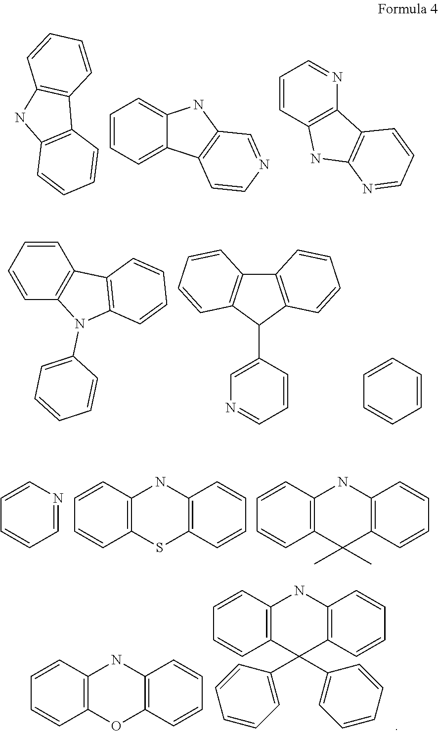
5. The compound according to claim 1, wherein Q is represented by one of Formula 4: ##STR00370##
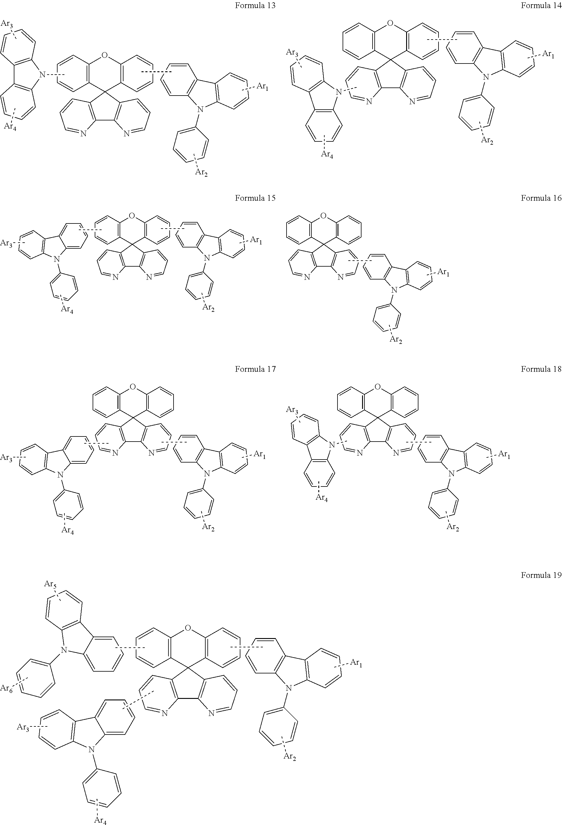
6. The compound according to claim 1, wherein the compound is represented by one of Formulas 5 to 22: ##STR00371## ##STR00372## ##STR00373## wherein each of Ar.sub.1 to Ar.sub.8 is independently selected from the group consisting of hydrogen, a substituted or non-substituted C.sub.6-C.sub.24 aryl group, a substituted or non-substituted C.sub.5-C.sub.24 heteroaryl group and CN.
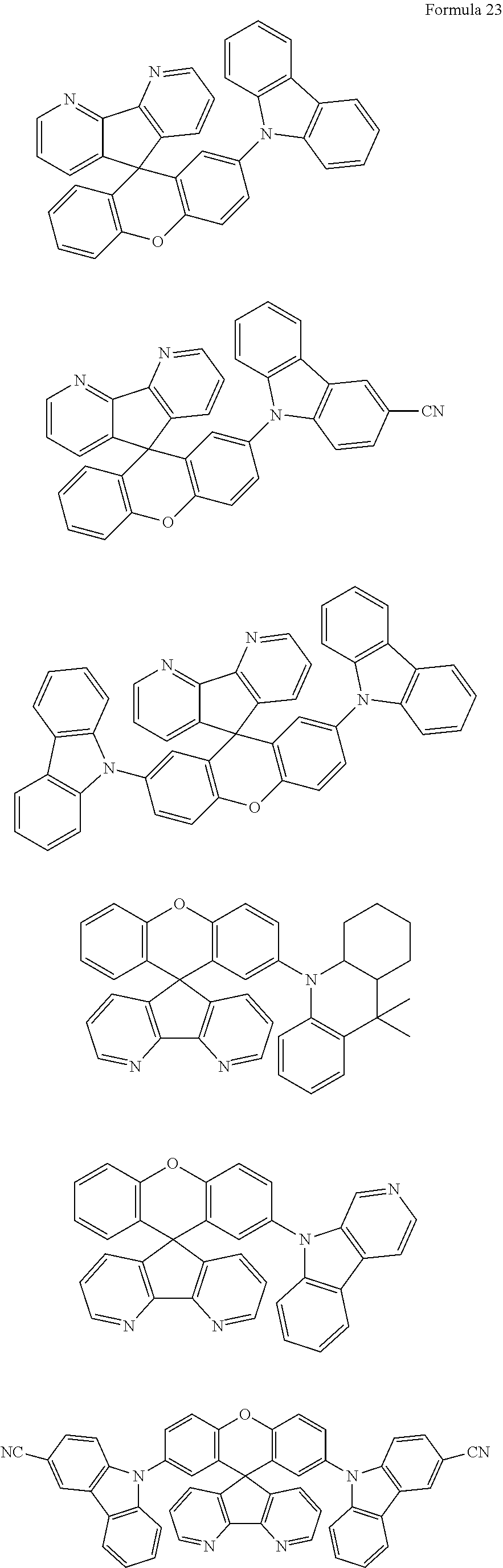
7. The compound according to claim 1, wherein the compound is one of Formula 23: ##STR00374## ##STR00375## ##STR00376##
8. An organic light emitting device, comprising: a first electrode; a second electrode facing the first electrode; and a first emitting material layer between the first electrode and the second electrode, the first emitting material layer including the compound of claim 1.
9. The organic light emitting device according to claim 8, wherein the first emitting material layer further includes a first host, and the compound is used as a first dopant.
10. The organic light emitting device according to claim 9, wherein an energy level of a singlet state of the first host is greater than a singlet state of the compound, or an energy level of a triplet state of the first host is greater than a triplet state of the compound.
11. The organic light emitting device according to claim 9, wherein the first emitting material layer further includes a fluorescent compound or a phosphorescent compound as a second dopant.
12. The organic light emitting device according to claim 9, further comprising: a second emitting material layer positioned between the first electrode and the first emitting material layer or between the first emitting material layer and the second electrode, wherein the second emitting material layer includes a second host and one of a fluorescent compound or a phosphorescent compound as a second dopant.
13. The organic light emitting device according to claim 8, wherein the first emitting material layer further includes a first dopant, and the compound is used as a first host.
14. The organic light emitting device according to claim 13, wherein a difference between an energy level of a highest occupied molecular orbital (HOMO) of the first host and an energy level of a HOMO of the first dopant or a difference between an energy level of a lowest unoccupied molecular orbital (LUMO) of the first host and an energy level of a LUMO of the first dopant is less than about 0.5 eV.
15. The organic light emitting device according to claim 13, wherein the first emitting material layer further includes a second dopant being one of a fluorescent compound or a phosphorescent compound, and wherein an energy level of a singlet state of the first dopant is greater than a singlet state of the second dopant.
16. The organic light emitting device according to claim 13, further comprising: a second emitting material layer including a second host and a second dopant being one of a fluorescent compound or a phosphorescent compound and positioned between the first electrode and the first emitting material layer.
17. The organic light emitting device according to claim 16, further comprising: a third emitting material layer including a third host and a third dopant being one of a fluorescent compound or a phosphorescent compound and positioned between the second electrode and the first emitting material layer.
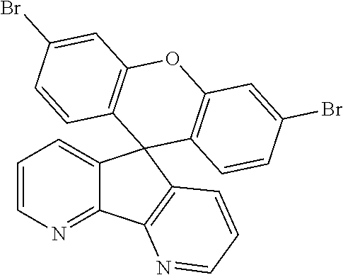
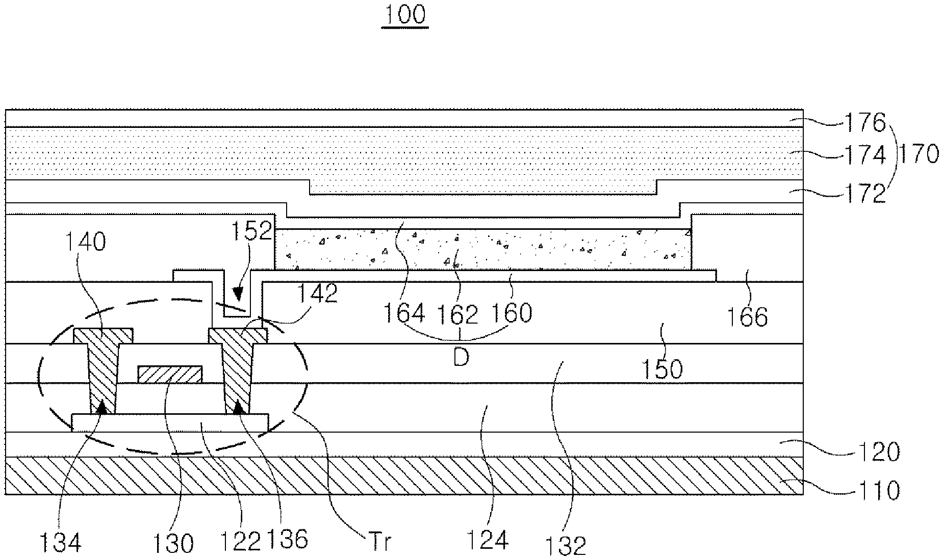
18. The organic light emitting device according to claim 8, wherein the compound is one of the following: ##STR00377## ##STR00378## ##STR00379##
19. An organic light emitting display device, comprising: a substrate; an organic light emitting device of claim 8 disposed on the substrate; and an encapsulation film covering the organic light emitting device.
20. The organic light emitting display device according to claim 19, wherein the compound is one of the following: ##STR00380## ##STR00381## ##STR00382##
Description
CROSS-REFERENCE TO RELATED APPLICATIONS
[0001] This application claims priority to and the benefit of Republic of Korea Patent Application No. 10-2018-0157114 filed on Dec. 7, 2018, which is hereby incorporated by reference in its entirety.
BACKGROUND
Technical Field
[0002] The present disclosure relates to a novel compound, and an organic light emitting device (OLED), and an organic light emitting display device including the compound.
Description of the Related Art
[0003] The material used in an organic layer of the OLED (organic light emitting diode) may be classified into an emitting material, a hole injection material, a hole transporting material, an electron transporting material, an electron injection material, and so on depending on their function. The emitting material may be classified into a high molecular weight material and a low molecular weight material depending on their molecular weight. The emitting material may be classified into a phosphorescent material and a fluorescent material depending on their emission mechanism. The emission of the fluorescent material is derived from a singlet excited state, while the emission of the phosphorescent is derived from a triplet excited state. In addition, the emitting material may be classified into a blue emitting material, a green emitting material and a red emitting material depending on their emission color. To provide excellent natural color, the emitting material may be further classified into a yellow emitting material and an orange emitting material.
[0004] To improve the color purity and the emission efficiency by the energy transfer, the host-guest system, i.e., host and dopant system, may be used. Namely, when the dopant, which has smaller energy band gap and higher emission efficiency than the host and higher, is doped into an emitting material layer, the exciton, which is generated in the host, is transferred into the dopant such that the light with high emission efficiency is provided.
[0005] However, the OLED using the related art emitting material has high driving voltage, low emission efficiency, and short lifespan. Accordingly, development of novel emitting material is required.
SUMMARY
[0006] Accordingly, the embodiment of the present disclosure is directed to a novel compound and an OLED and an organic light emitting display device using the same that substantially obviate one or more of the problems due to limitations and disadvantages of the related art.
[0007] Additional features and advantages of the disclosure will be set forth in the description which follows, and in part will be apparent from the description, or may be learned by practice of the disclosure. The objectives and other advantages of the disclosure will be realized and attained by the structure particularly pointed out in the written description and claims hereof as well as the appended drawings.
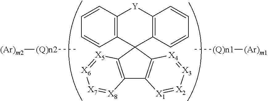
[0008] To achieve these and other advantages and in accordance with the purpose of the embodiments of the disclosure, as embodied and broadly described herein, embodiments relate to a compound of
##STR00002##
wherein Y is CR.sub.1R.sub.2, O or S, and each of R.sub.1 and R.sub.2 is independently selected from the group consisting of hydrogen, substituted or non-substituted C.sub.6-C.sub.24 aryl group and substituted or non-substituted C.sub.5-C.sub.24 heteroaryl group, wherein each of X.sub.1 to X.sub.8 is independently selected from C or N, and at least one of X.sub.1 to X.sub.8 is N, wherein Q is independently selected from the group consisting of substituted or non-substituted C.sub.6-C.sub.60 aryl group, substituted or non-substituted C.sub.5-C.sub.60 heteroaryl group, CN and NR.sub.3R.sub.4, and each of R.sub.3 and R.sub.4 is independently selected from the group consisting of hydrogen, substituted or non-substituted C.sub.6-C.sub.60 aryl group and substituted or non-substituted C.sub.5-C.sub.60 heteroaryl group, wherein Ar is independently selected from the group consisting of substituted or non-substituted C.sub.1-C.sub.20 alkyl group, substituted or non-substituted C.sub.6-C.sub.24 aryl group, substituted or non-substituted C.sub.5-C.sub.24 heteroaryl group, CN and NR.sub.5R.sub.6, and each of R.sub.5 and R.sub.6 is independently selected from the group consisting of hydrogen, substituted or non-substituted C.sub.6-C.sub.24 aryl group and substituted or non-substituted C.sub.5-C.sub.24 heteroaryl group, and wherein n1, n2, m1 and m2 is one of 0, 1 and 2, and at least one of n1 and n2 is 1 or more.
[0009] Embodiments also relate to an organic light emitting device including a first electrode, a second electrode facing the first electrode, and a first emitting material layer between the first and second electrodes and including a compound.
[0010] Embodiments also relate to an organic light emitting display device including a substrate, an organic light emitting device on the substrate, and an encapsulation film covering the organic light emitting diode.
[0011] It is to be understood that both the foregoing general description and the following detailed description are by example and explanatory and are intended to provide further explanation of the disclosure as claimed.
BRIEF DESCRIPTION OF THE DRAWINGS
[0012] The accompanying drawings, which are included to provide a further understanding of the disclosure and are incorporated in and constitute a part of this specification, illustrate embodiments of the disclosure and together with the description serve to explain the principles of the disclosure.
[0013] FIG. 1 is a schematic cross-sectional view of an organic light emitting display device according to the present disclosure.
[0014] FIG. 2 is a schematic cross-sectional view of an OLED according to a first embodiment of the present disclosure.
[0015] FIG. 3 is a schematic cross-sectional view of an OLED according to a second embodiment of the present disclosure.
[0016] FIG. 4 is a schematic cross-sectional view of an OLED according to a third embodiment of the present disclosure.
DETAILED DESCRIPTION
[0017] Reference will now be made in detail to example embodiments, examples of which are illustrated in the accompanying drawings.
[0018] In the description, the term of "aryl" may be a C.sub.5-C.sub.30 aromatic hydrocarbon ring, e.g., phenyl, benzyl, naphthyl, biphenyl, terphenyl, fluorenyl, phenanthrenyl, triphenylenyl, perylenyl, chrysenyl, fluoranthenyl, benzofluorenyl, benzotriphenylenyl, benzochrysenyl, anthracenyl, stilbenyl or pyrenyl, and the term of "heteroaryl" may be a C.sub.3-C.sub.30 aromatic ring including at least one hetero-atom, e.g., pyrrolyl, pyrazinyl, pyridinyl, indolyl, isoindoleyl, furyl, benzofuranyl, isobenzofuranyl, dibenzofuranyl, benzothiophenyl, dibenzothiophenyl, quinolyl, isoquinolyl, quinoxalinyl, carbazolyl, phenanthridinyl, acridinyl, phenanthrolinyl, thienyl, pyridine ring, pyrazine ring, pyrimidine ring, pyridazine ring, triazine ring, indole ring, quinoline ring, acridine ring, pyrrolidine ring, dioxane ring, piperidine ring, morpholine ring, piperazine ring, carbazole ring, furan ring, thiophene ring, oxazole ring, oxadiazole ring, benzoxazole ring, thiazol ring, thiadiazole ring, benzothiazole ring, triazole ring, imidazole ring, benzoimidazole ring, pyran ring or dibenzofuran ring.
[0019] When a compound and/or a moiety is referred to as being "substituted", the compound and/or the moiety may be substituted by at least one selected from the group consisting of deuterium, halogen, amino group, nitrile group, nitro group, C.sub.1-C.sub.20 alkyl group, C.sub.2-C.sub.20 alkenyl group, C.sub.1-C.sub.20 alkoxy group, C.sub.3-C.sub.20 cycloalkyl group, C.sub.3-C.sub.20 heterocycloalkyl group, C.sub.6-C.sub.30 aryl group and C.sub.3-C.sub.30 heteroaryl group.
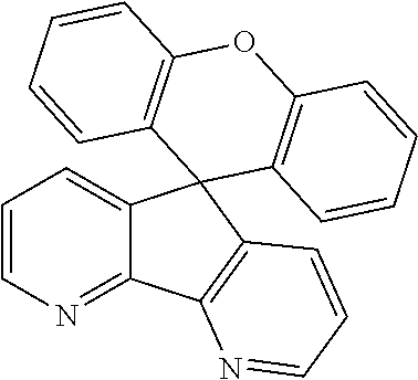
[0020] The present disclosure provides a compound represented by Formula 1. Formula 1
##STR00003##
[0021] In Formula 1, Y is CR.sub.1R.sub.2, O or S, and each of R.sub.1 and R.sub.2 is independently selected from the group consisting of hydrogen, substituted or non-substituted C.sub.6-C.sub.24 aryl group and substituted or non-substituted C.sub.5-C.sub.24 heteroaryl group. Each of X.sub.1 to X.sub.8 is independently selected from C or N, and at least one of X.sub.1 to X.sub.8 is N.
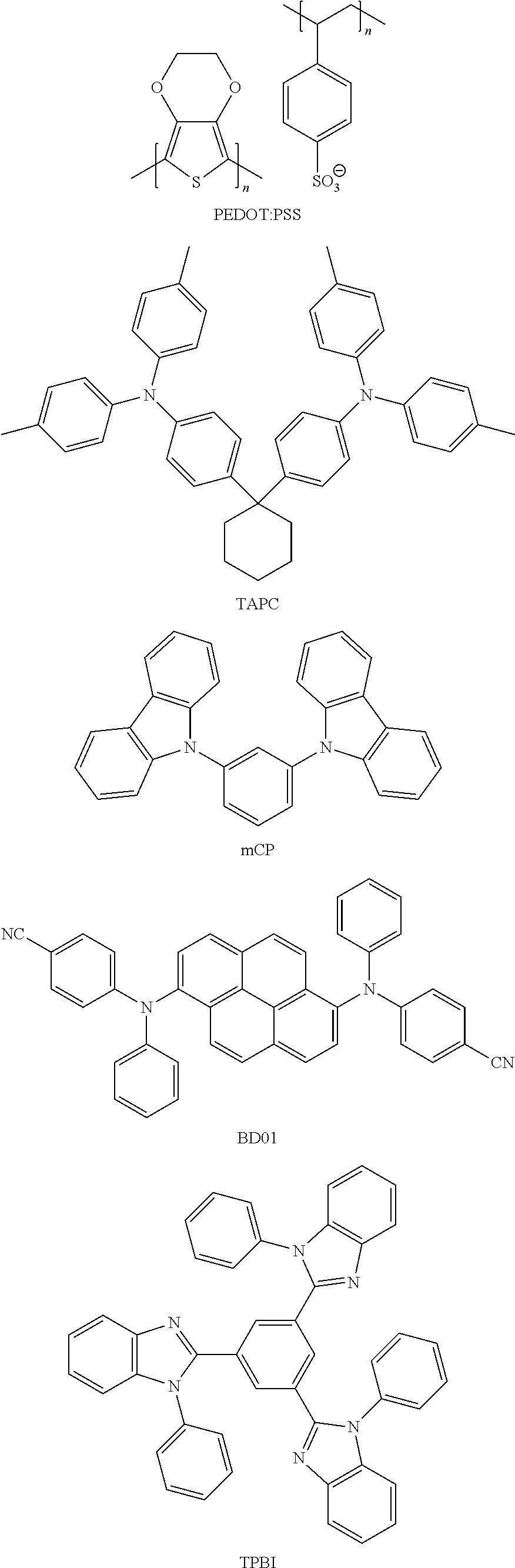
[0022] Q is independently selected from the group consisting of substituted or non-substituted C.sub.6-C.sub.60 aryl group, substituted or non-substituted C.sub.5-C.sub.60 heteroaryl group, CN and NR.sub.3R.sub.4, and each of R.sub.3 and R.sub.4 is independently selected from the group consisting of hydrogen, substituted or non-substituted C.sub.6-C.sub.60 aryl group and substituted or non-substituted C.sub.5-C.sub.60 heteroaryl group.
[0023] Ar is independently selected from the group consisting of substituted or non-substituted C.sub.1-C.sub.20 alkyl group, substituted or non-substituted C.sub.6-C.sub.24 aryl group, substituted or non-substituted C.sub.5-C.sub.24 heteroaryl group, CN and NR.sub.5R.sub.6, and each of R.sub.5 and R.sub.6 is independently selected from the group consisting of hydrogen, substituted or non-substituted C.sub.6-C.sub.24 aryl group and substituted or non-substituted C.sub.5-C.sub.24 heteroaryl group.
[0024] Each of n1, n2, m1 and m2 is one of 0, 1 and 2, and at least one of n1 and n2 is 1 or more.
[0025] For example, Ar may independently be a t-butyl group, a carbazole group, a cyano group (CN), a phenoxazine group, a carbonyl group.
[0026] Since the compound of the present disclosure may provide fluorescent emission or delayed fluorescent emission, the compound may be used as an organic emitting material.
[0027] According to an embodiment of the present disclosure, the compound may be used alone or in combination with a known compound in an emitting layer of the organic light emitting device. The compound according to the present disclosure may be used as a dopant of a known host material. In addition, known materials can be used as dopants, and the compounds of the present disclosure may be used as an assist dopant.
[0028] The compound of the present disclosure has a triplet energy suitable for a blue fluorescent host by introducing diazafluorene having a spiro-structure such that deep blue emission of high color purity can be provided.
[0029] In addition, the HOMO and LUMO molecular orbital function can be separated by the structural characteristics of spiro-diazafluorene, and the charge balance in the emitting layer can be controlled by the bipolar characteristics. Accordingly, high emitting efficiency is provided.
[0030] In addition, the compound according to an embodiment of the present disclosure can be used as a thermally activated delayed fluorescence host material to minimize the difference between the excited singlet energy and the excited triplet energy (.DELTA.E.sub.ST) such that high emitting efficiency is provided.
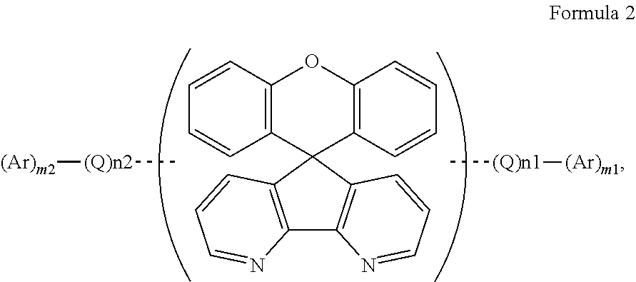
[0031] In an embodiment of the present disclosure, the compound may be represented by Formula 2.
##STR00004##
[0032] In Formula 2, the definition of Ar, Q, n1, n2, ml and m2 is the same as in Formula 1.
[0033] Since Y is fixed to oxygen atom in Formula 2, the energy level of HOMO and LUMO of the compound is adjusted. In addition, the diazafluorene core has a high triplet (T1) energy level. Accordingly, the compound provides properties of high efficiency, long lifespan and low driving voltage.
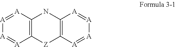
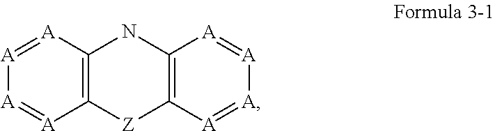
[0034] Q in Formula 1 and/or Formula 2 may be represented by Formula 3-1.
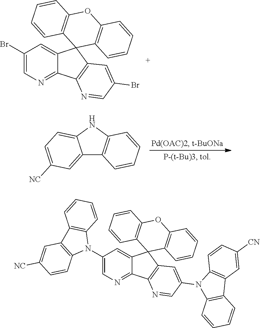
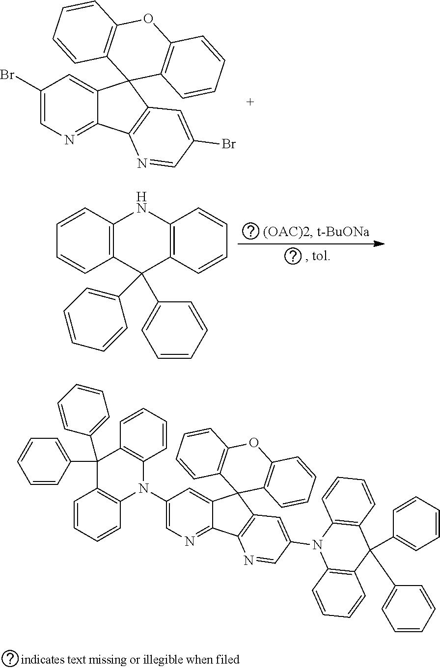
##STR00005##
[0035] In Formula 3-1, Z is a single bond, S, O or CR.sub.7R.sub.8, and each of R.sub.7 and R.sub.8 is independently selected from the group consisting of hydrogen and C.sub.1-C.sub.24 alkyl group. A is C or N.
[0036] When Q has a structure of Formula 3-1, electrons may be provided such that the HOMO energy level of the compound may be controlled.
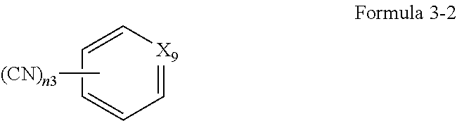
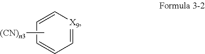
[0037] Alternatively, Q in Formula 1 and/or Formula 2 may be represented by Formula 3-2.
##STR00006##
[0038] In Formula 3-2, X.sub.9 is carbon or nitrogen, and n3 is 0 or 1.
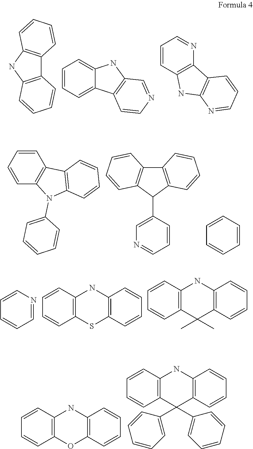
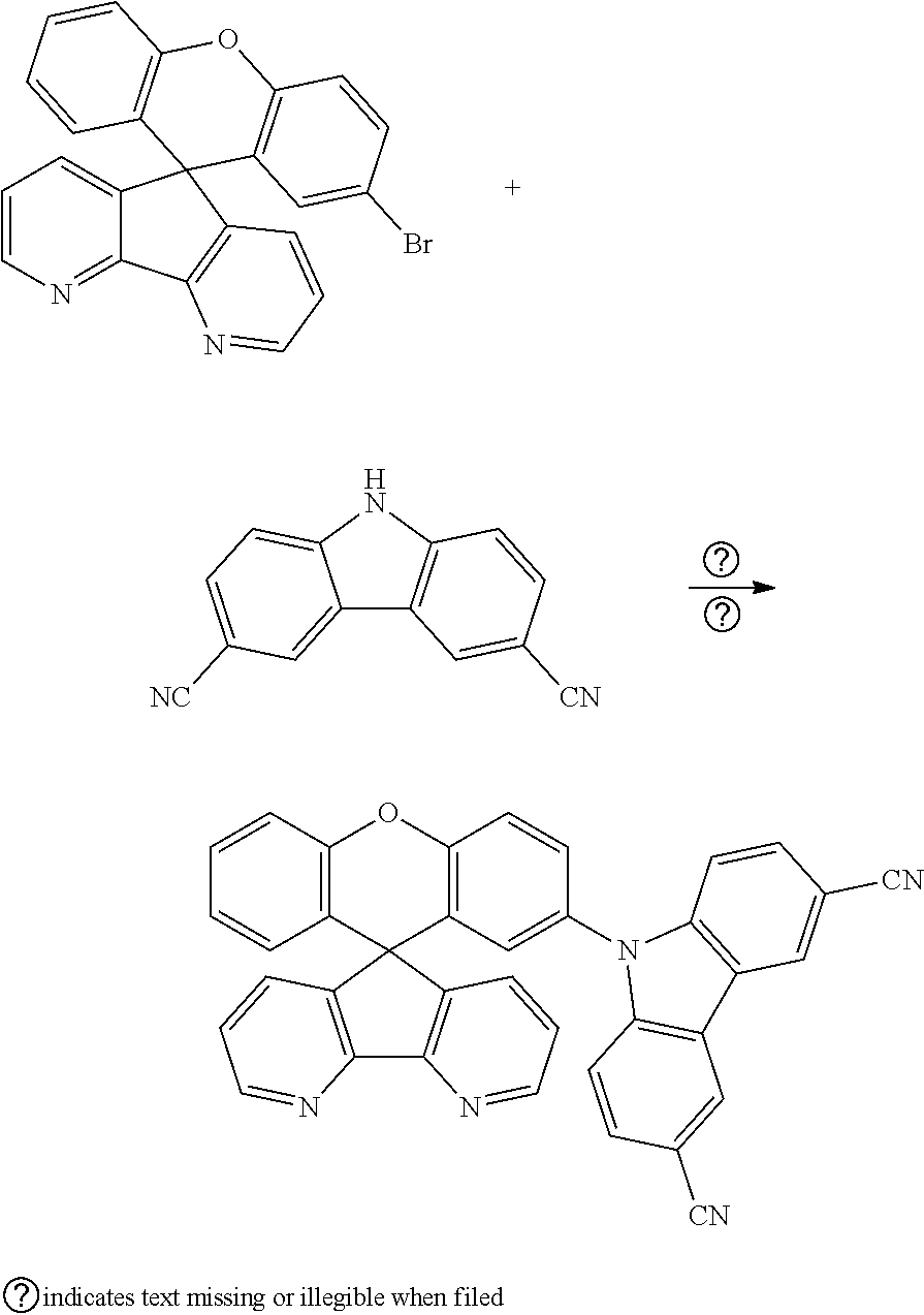
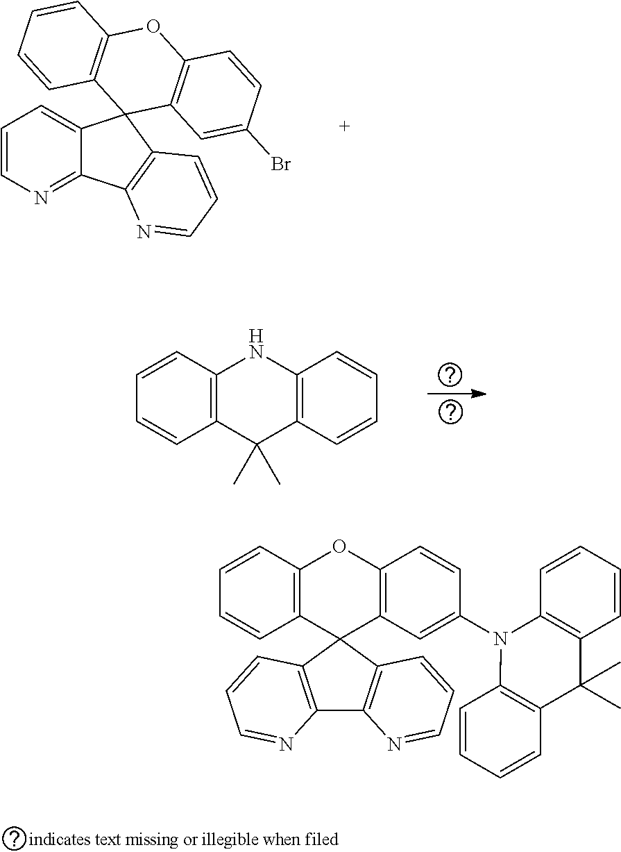
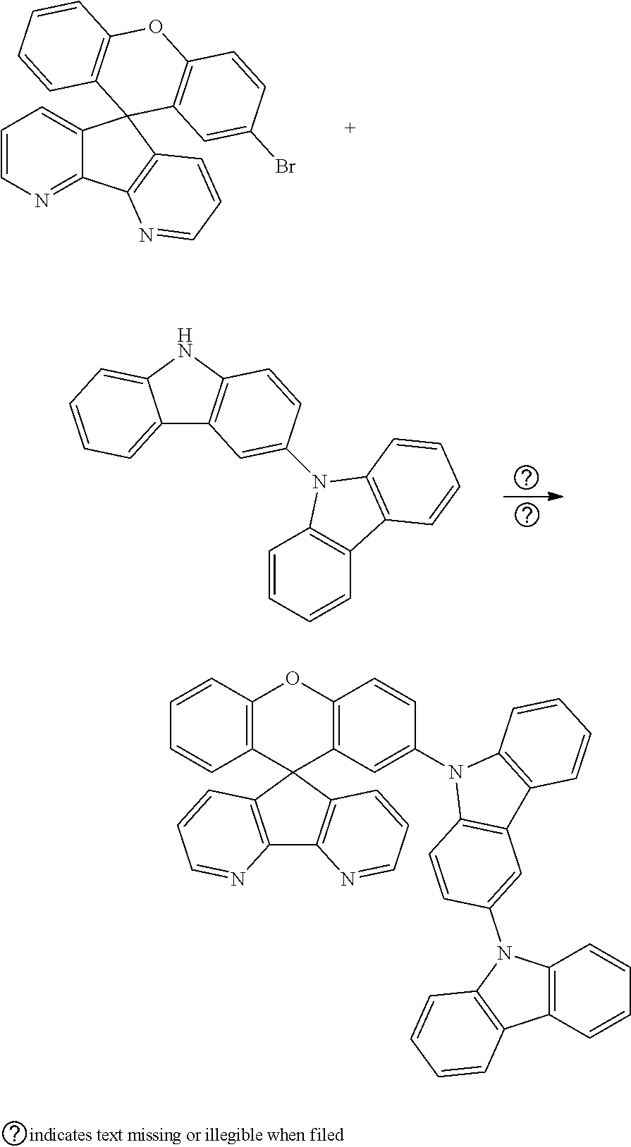
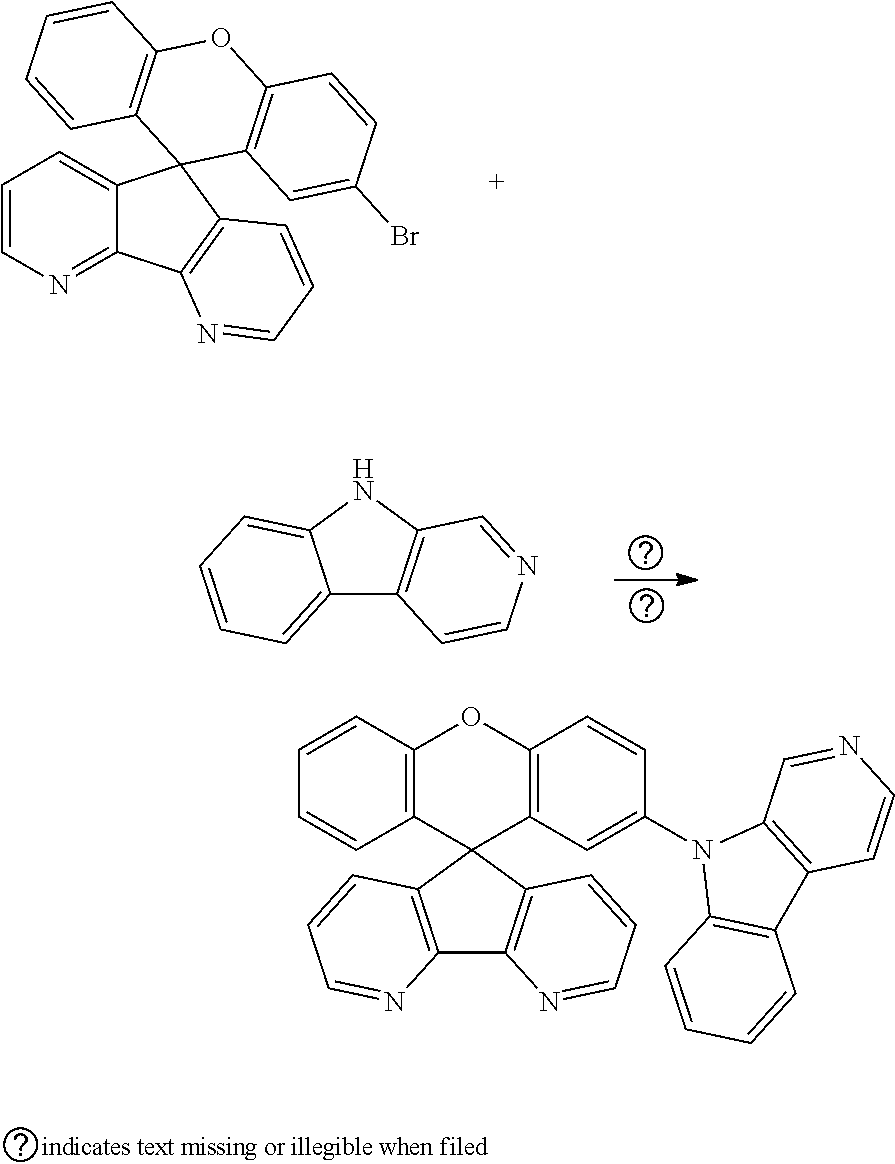
[0039] Alternatively, Q in Formula 1 and/or Formula 2 may be one of Formula 4.
##STR00007##
[0040] When Q has a structure of Formula 4, electrons may be provided such that the HOMO energy level of the compound may be controlled.
[0041] In an embodiment of the present disclosure, the compound may be represented by one of Formulas 5 to 22.
##STR00008## ##STR00009## ##STR00010##
[0042] In Formulas 5 to 22, each of Ar.sub.1 to Ar.sub.8 may independently be hydrogen, a substituted or non-substituted C.sub.6-C.sub.24 aryl group, a substituted or non-substituted C.sub.5-C.sub.24 heteroaryl group, or CN. For example, each of Ar.sub.1 to Ar.sub.8 may independently be a t-butyl group, a carbazole group, a cyano group (CN), a phenoxazine group, or a carbonyl group.
[0043] The compound of the present disclosure may be one of following.
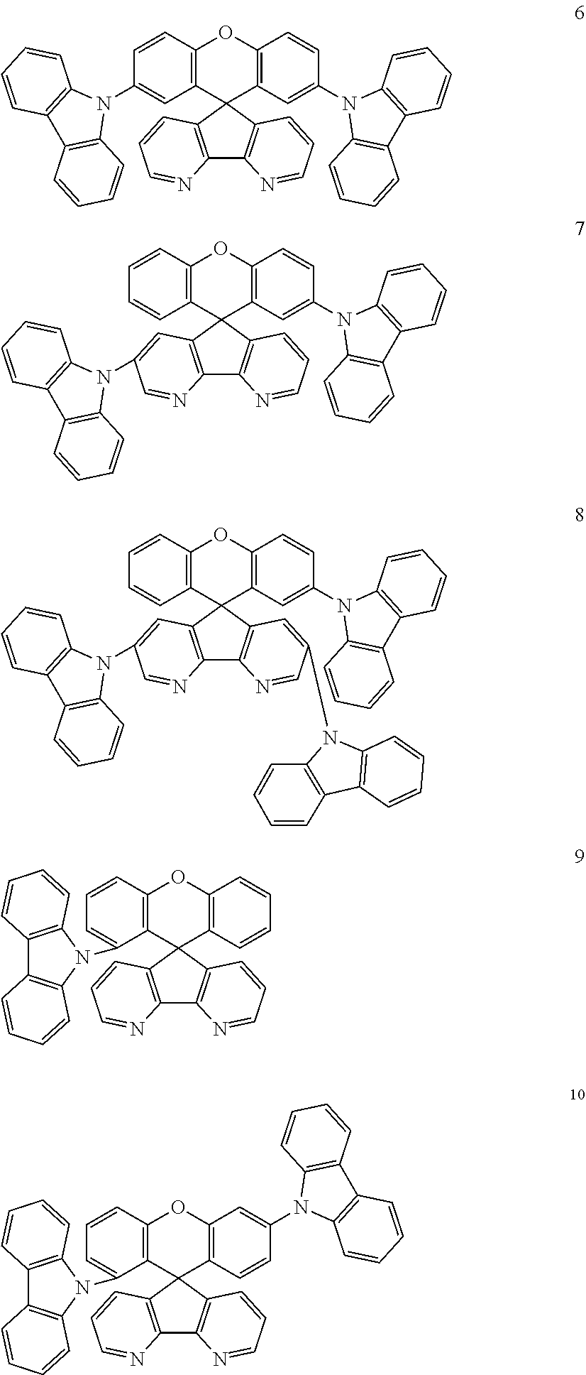
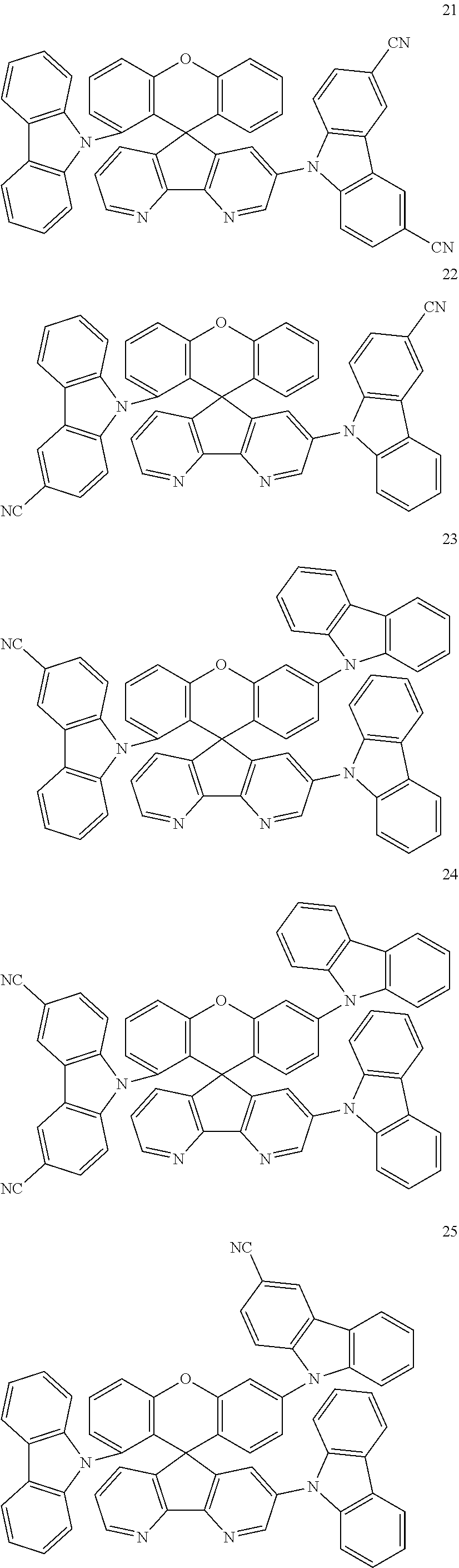
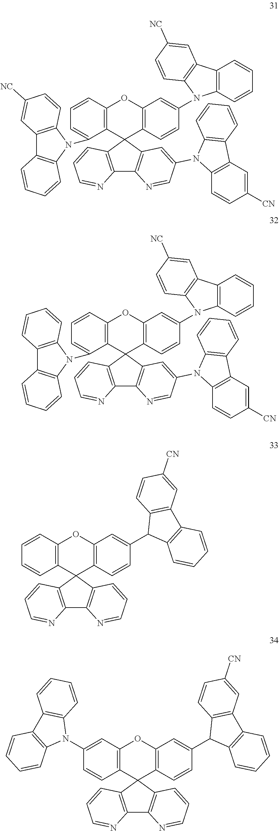
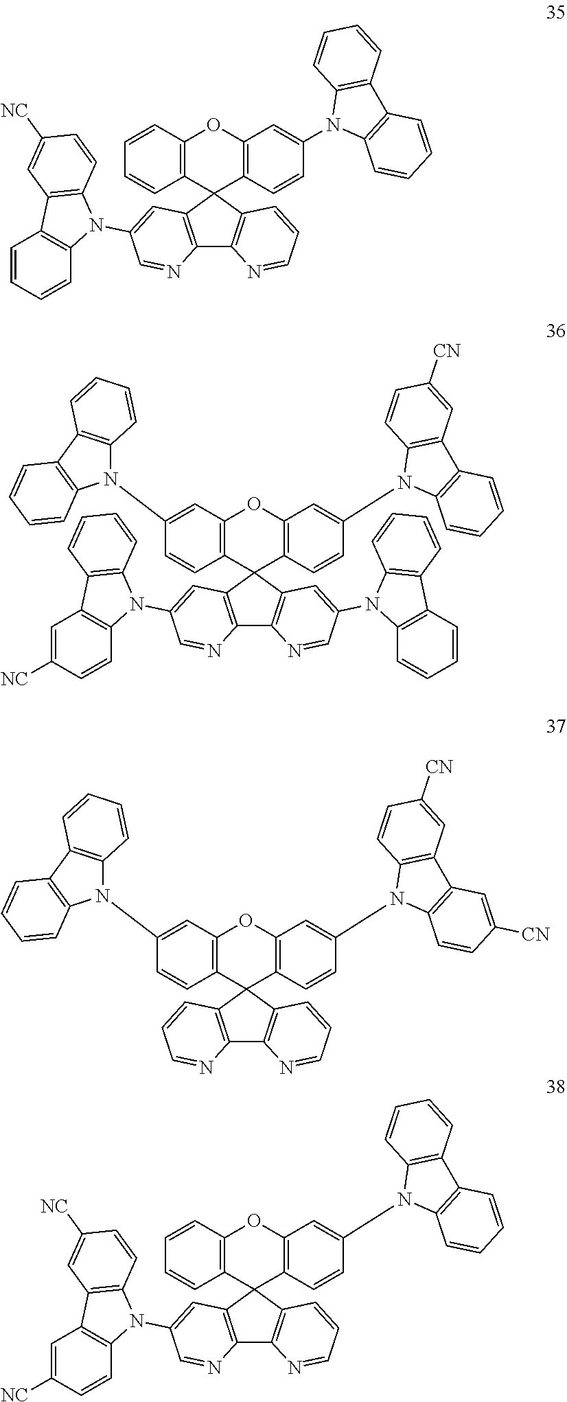
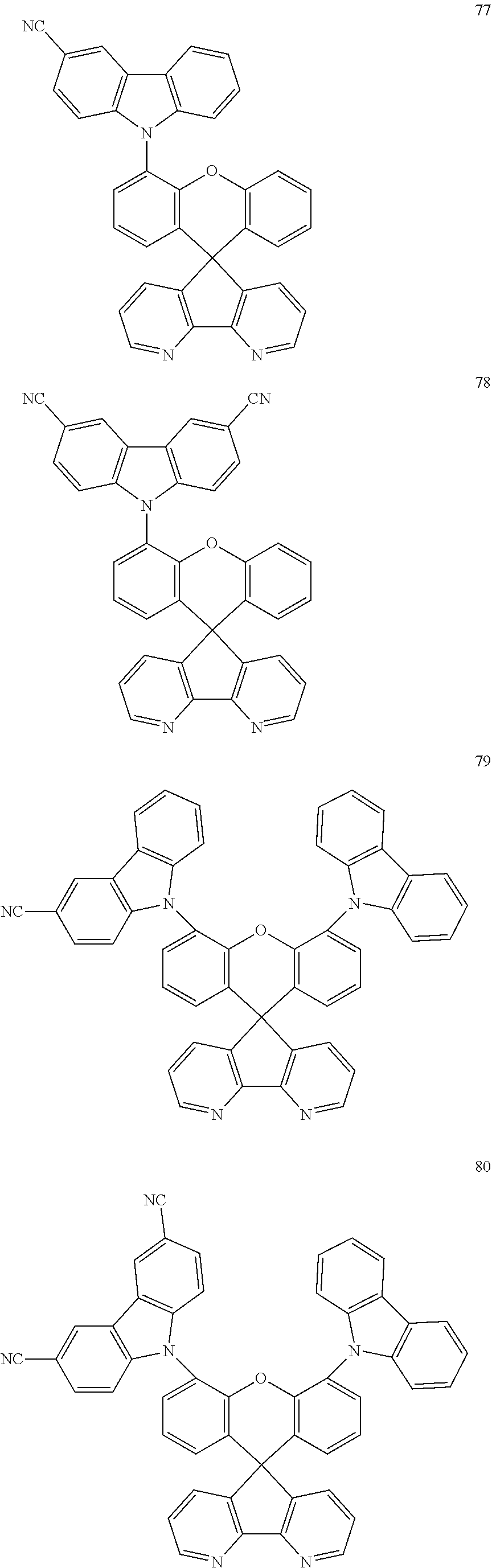
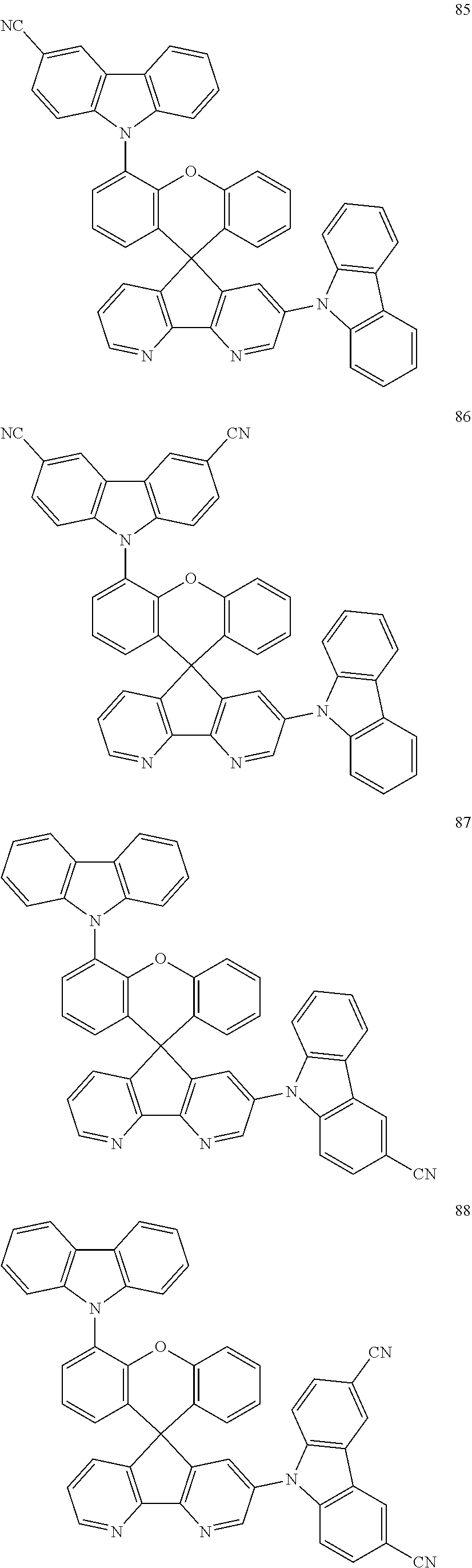
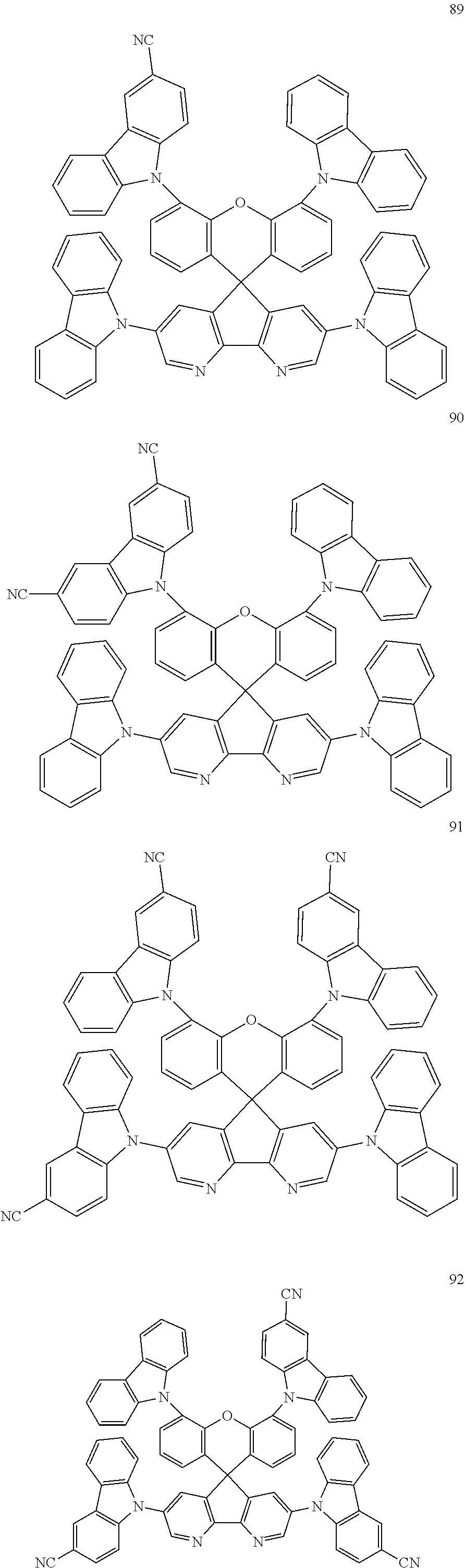
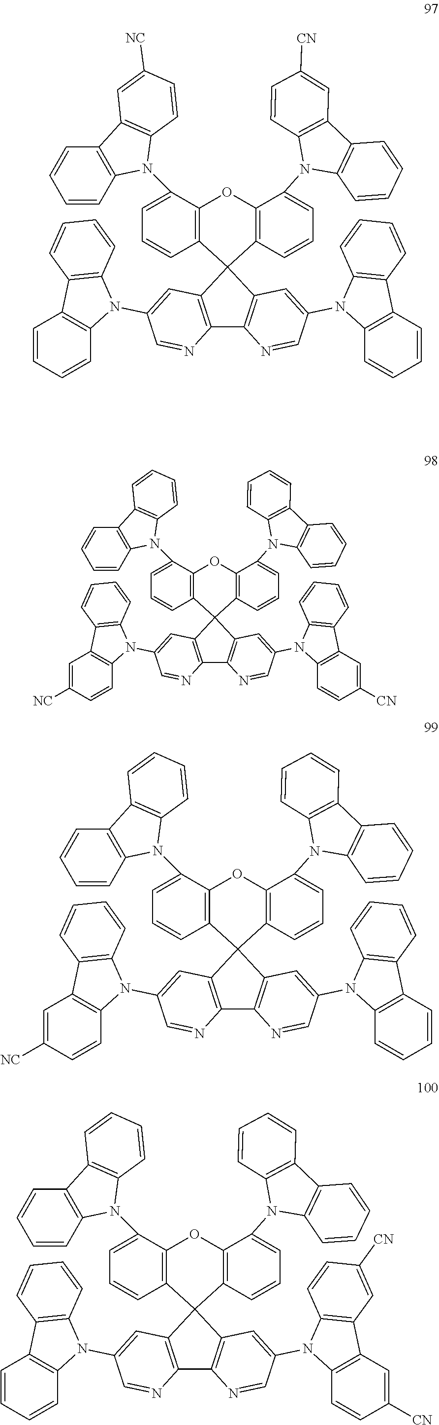
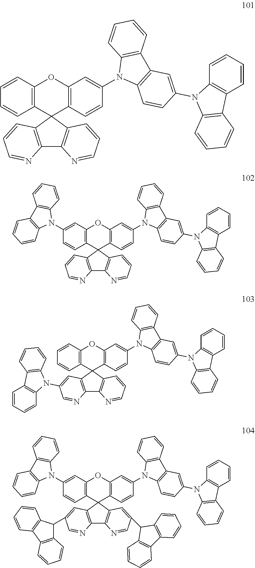
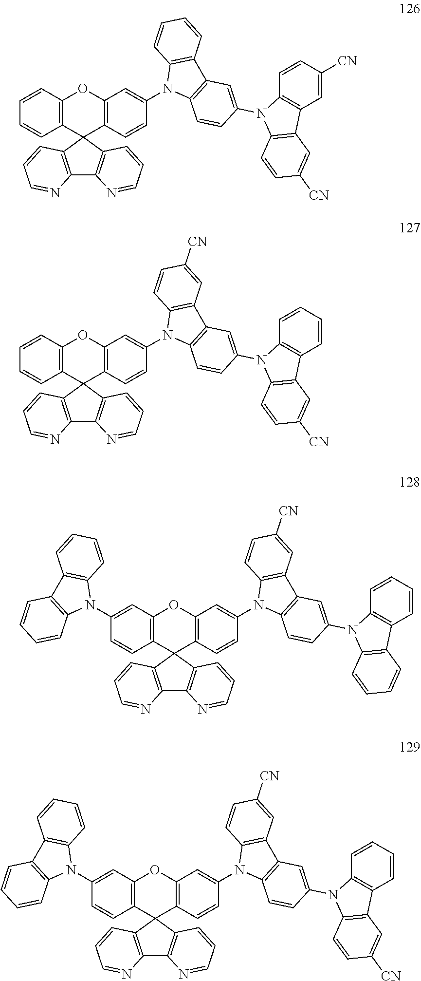
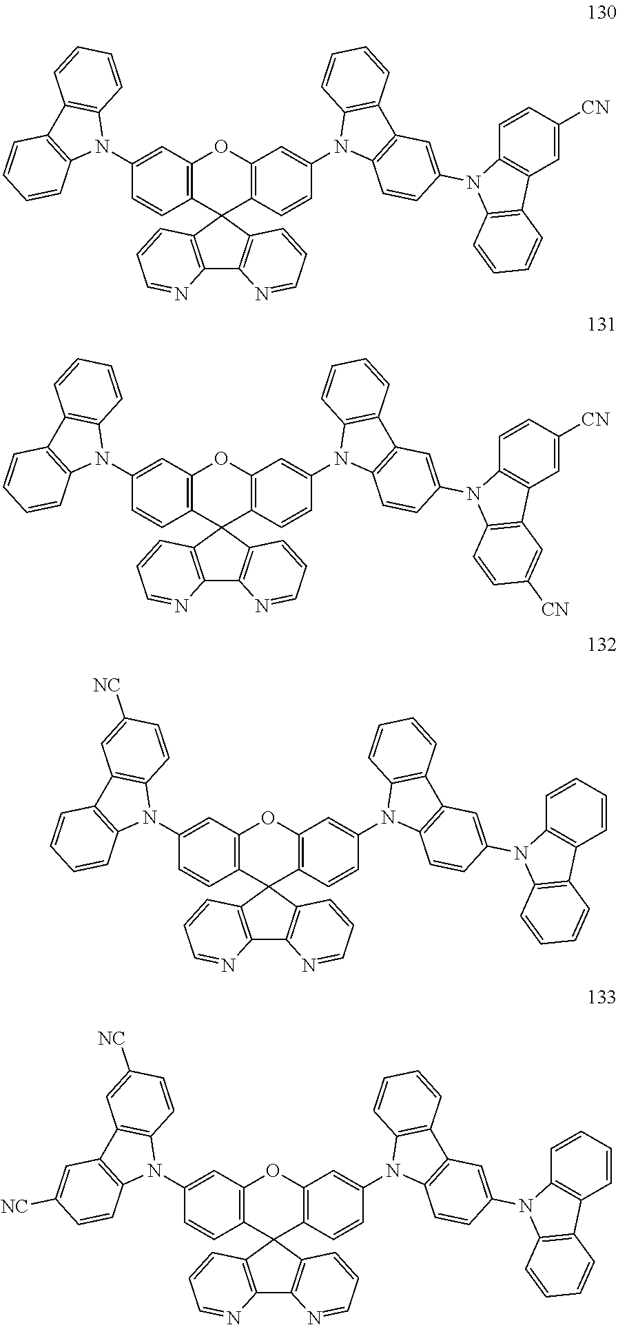
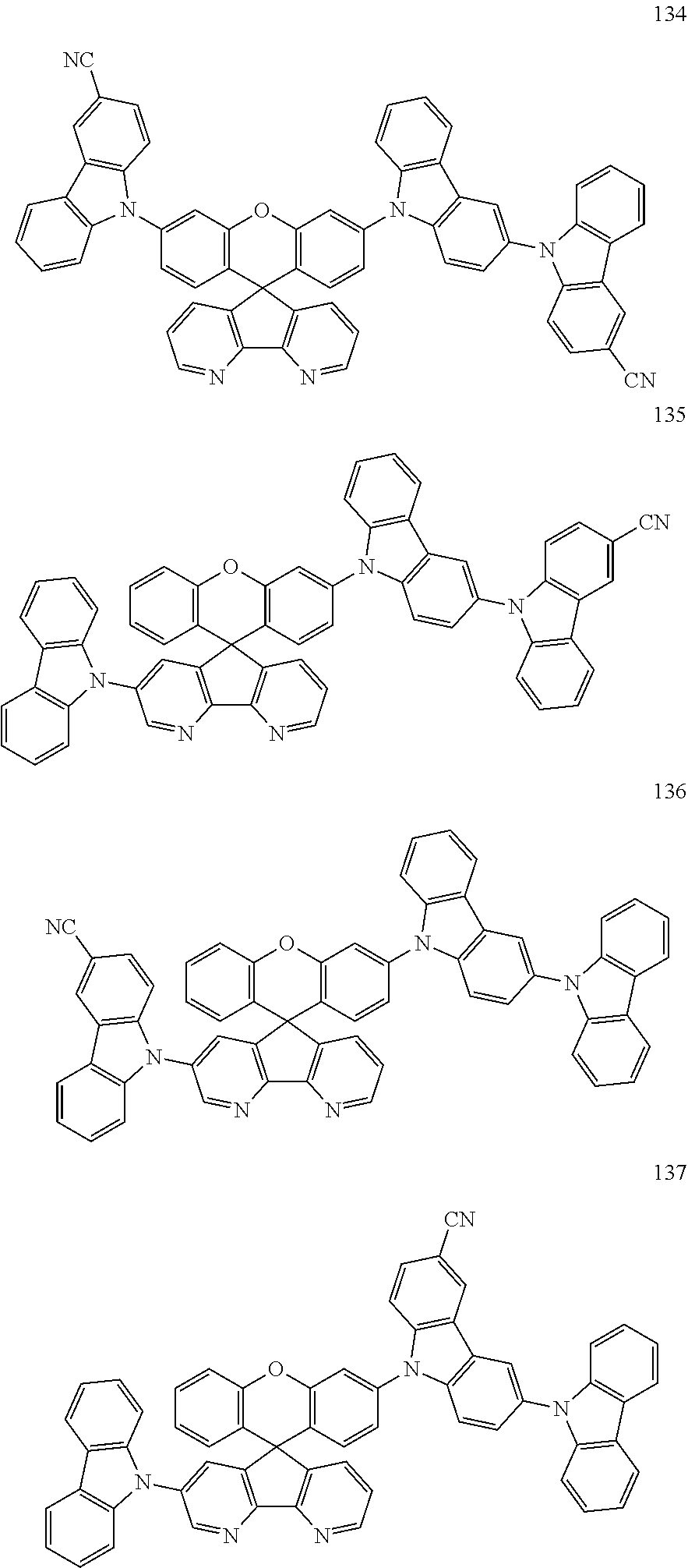
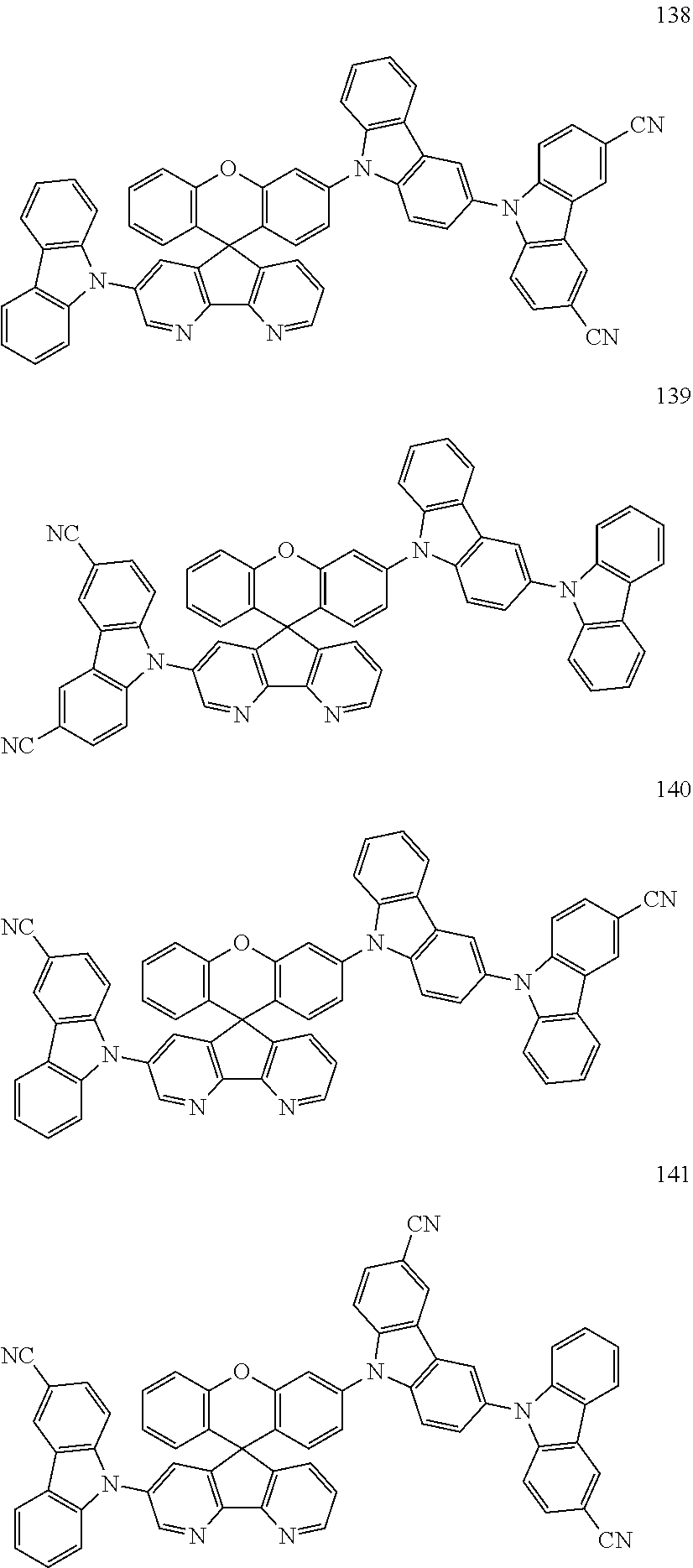
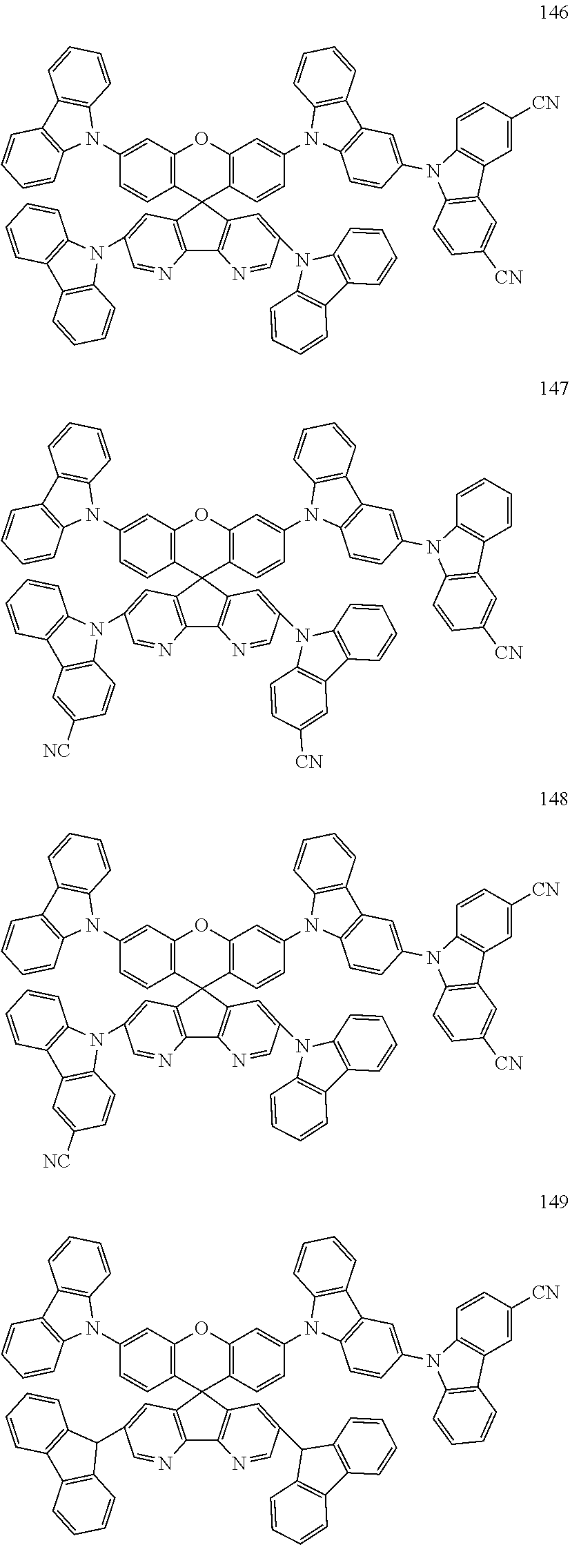
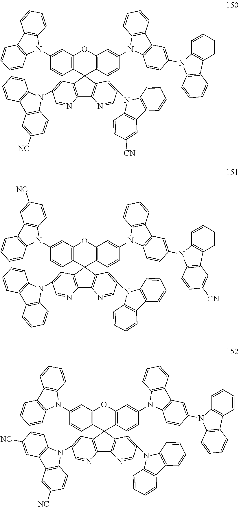
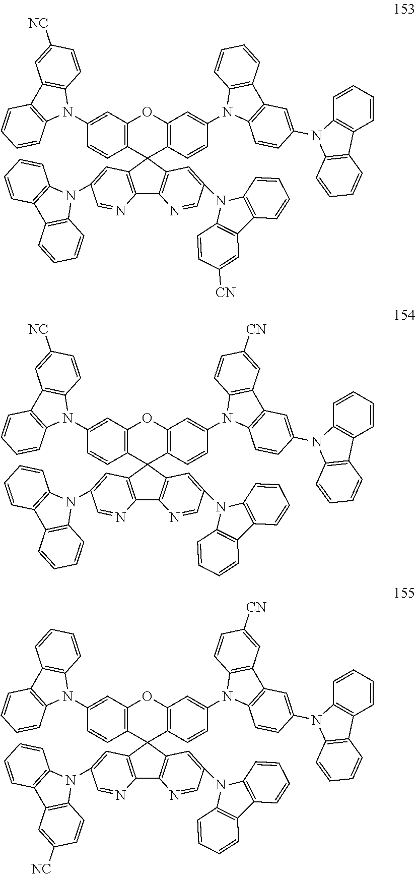
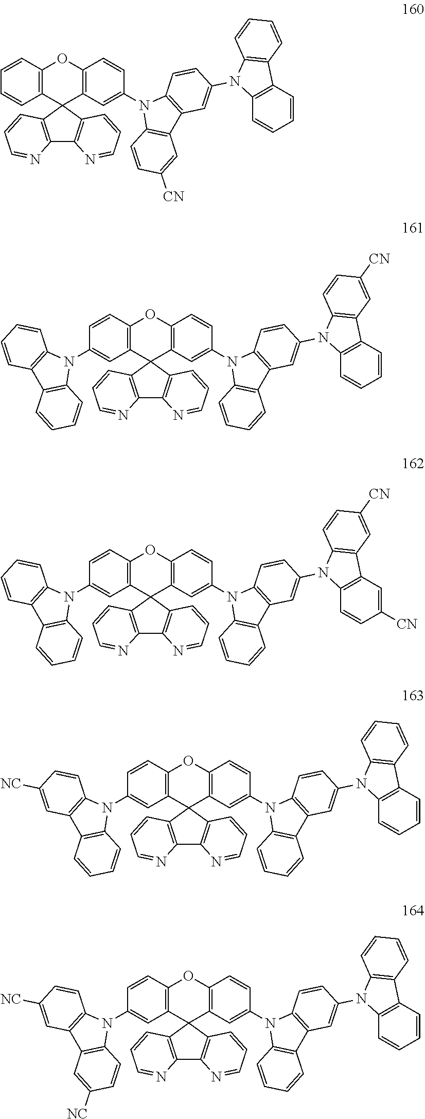
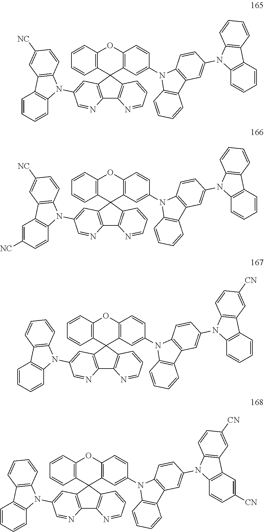
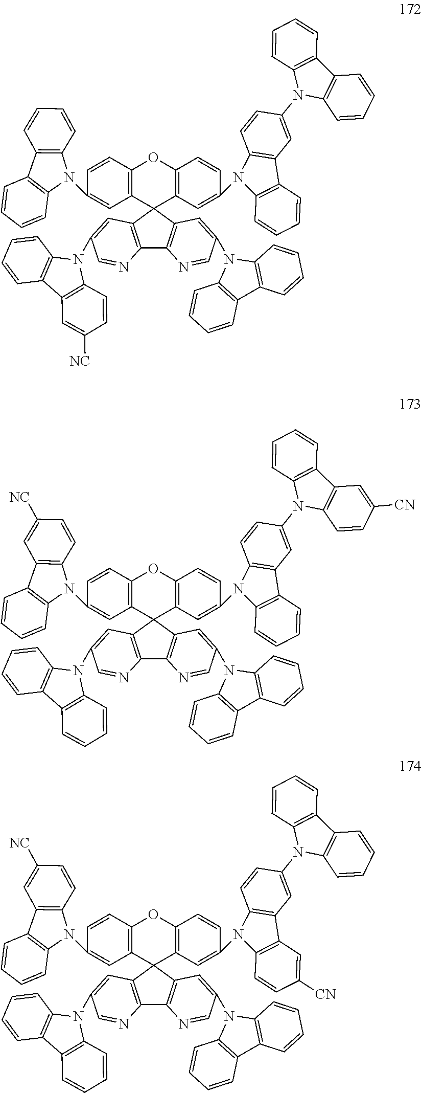
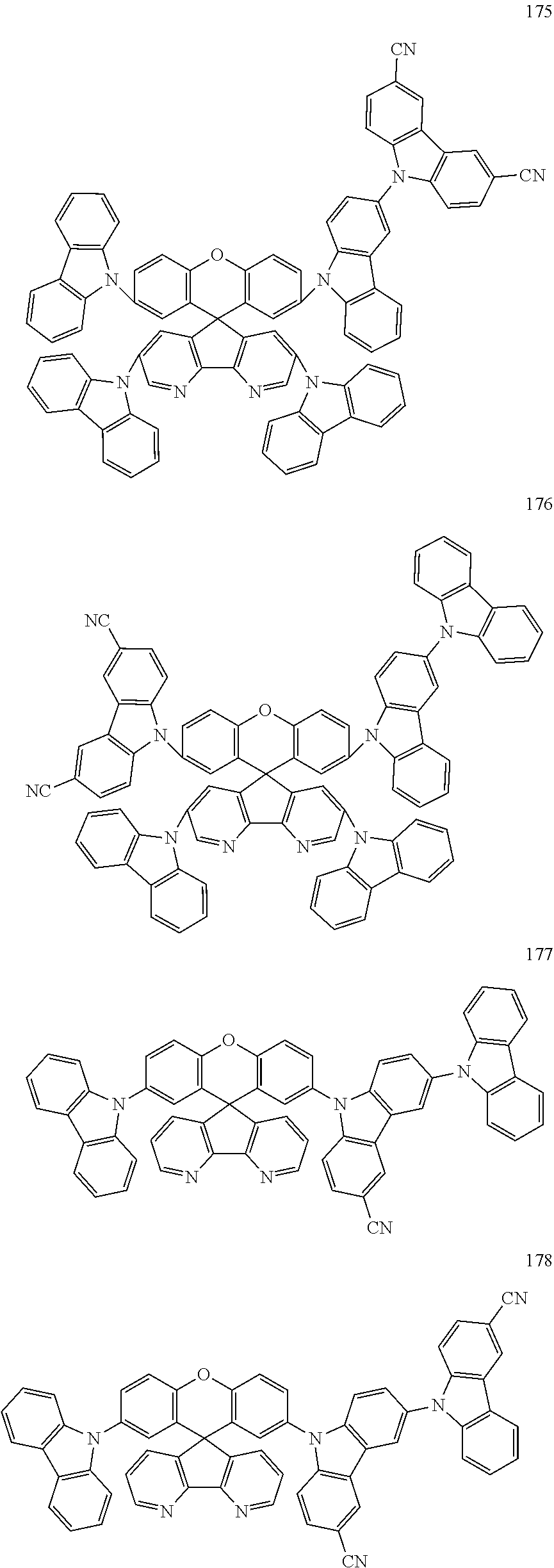
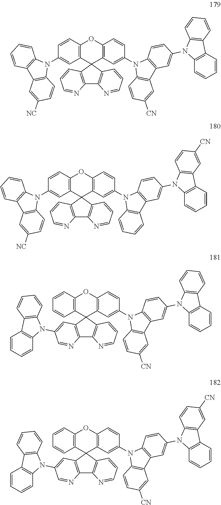
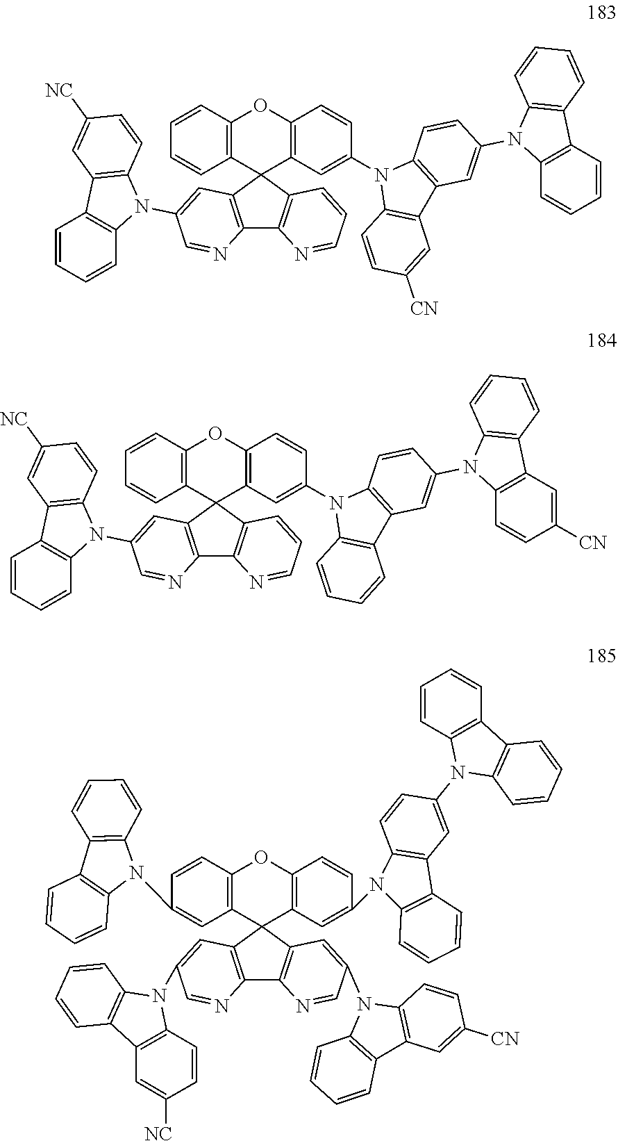
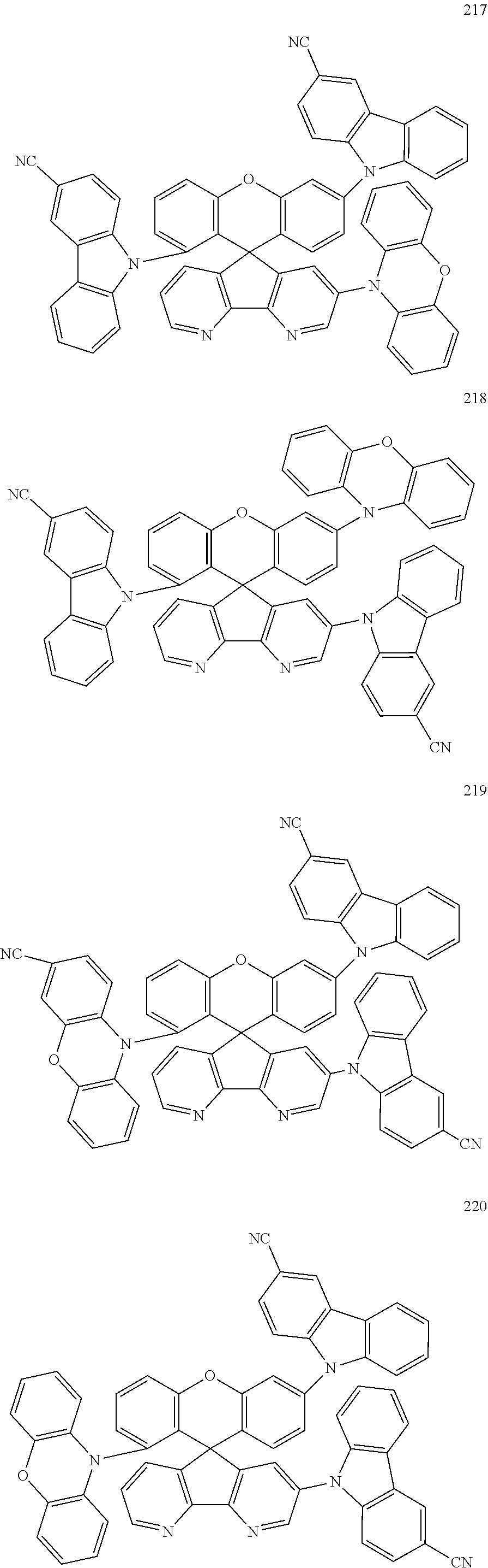
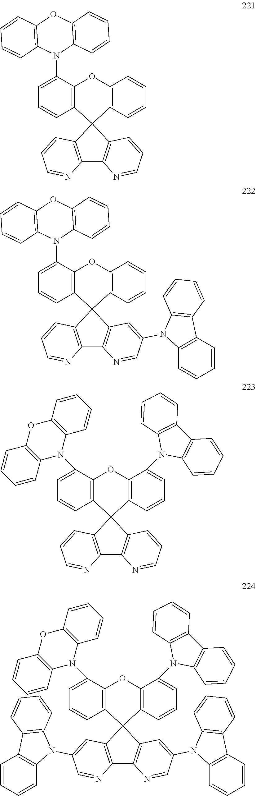
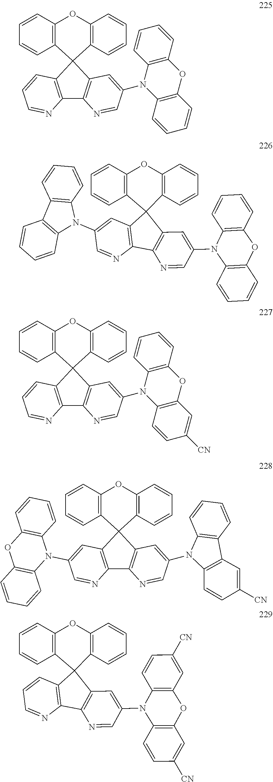
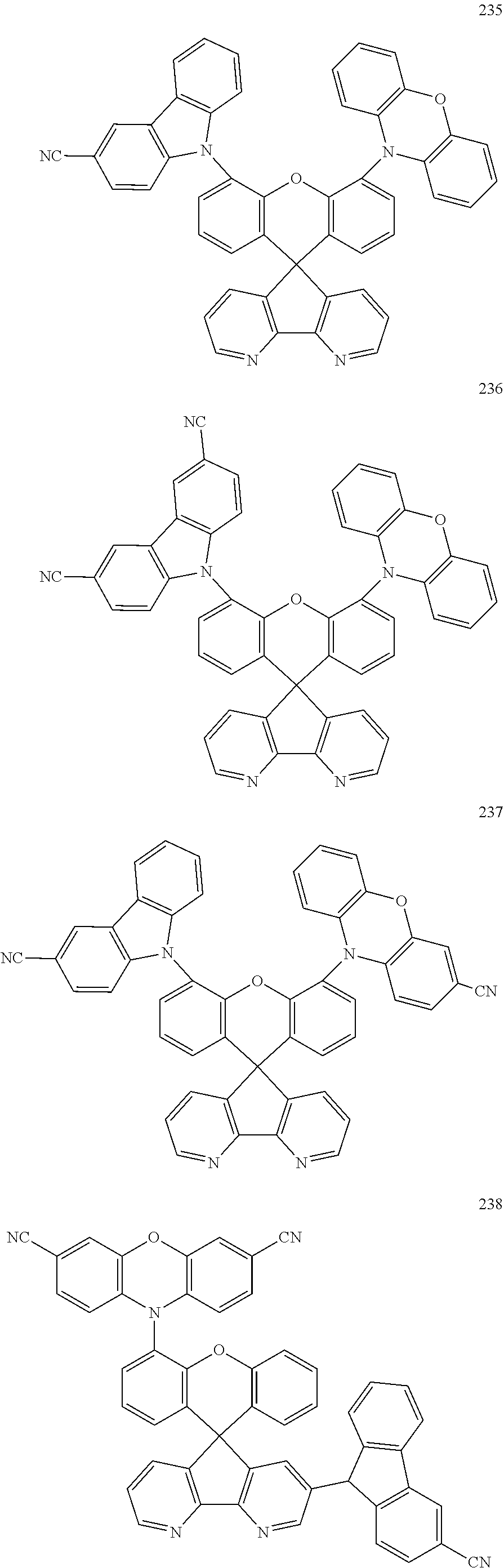
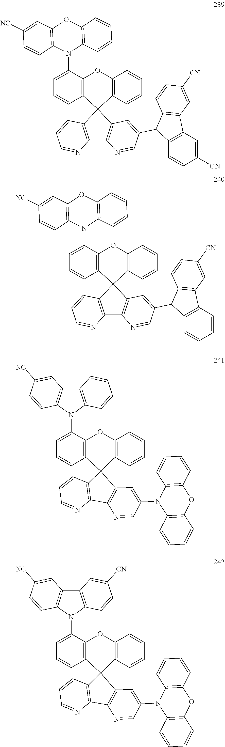
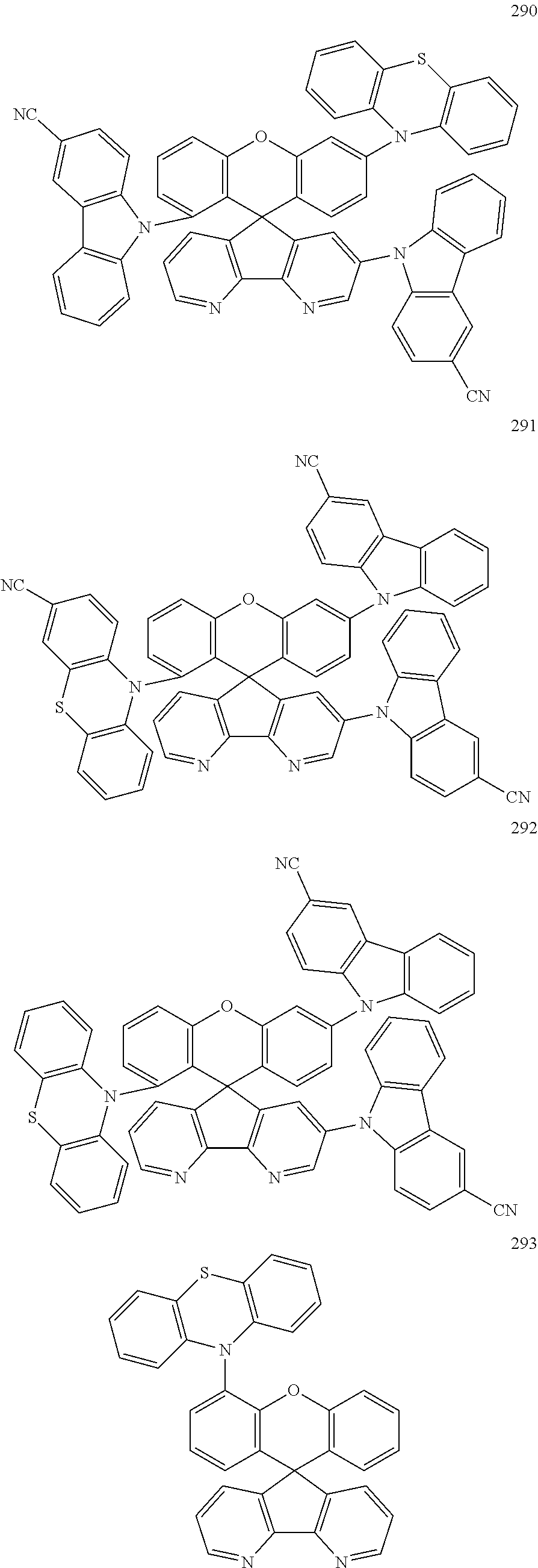
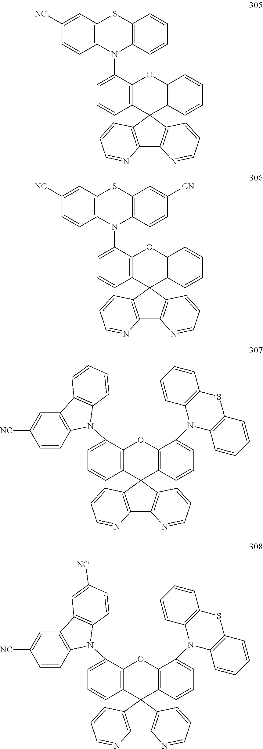
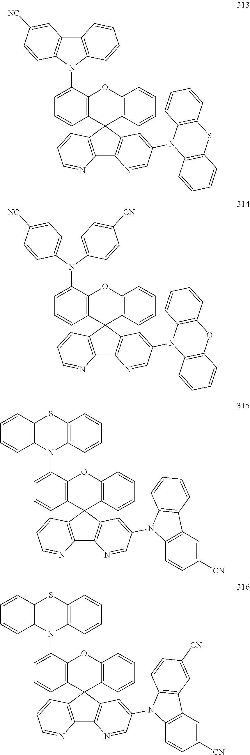
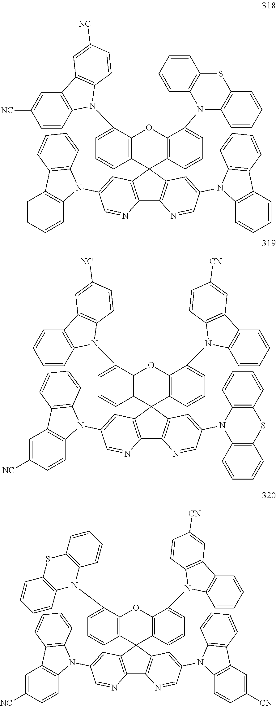
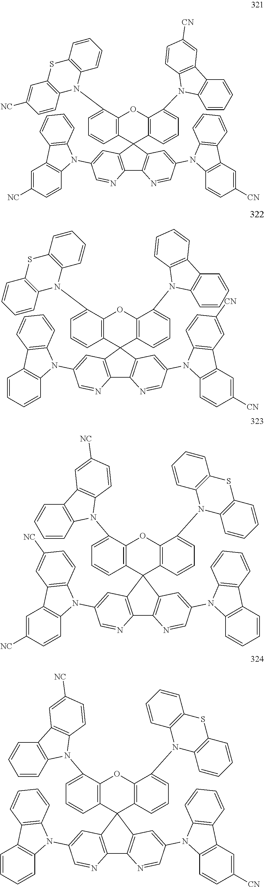
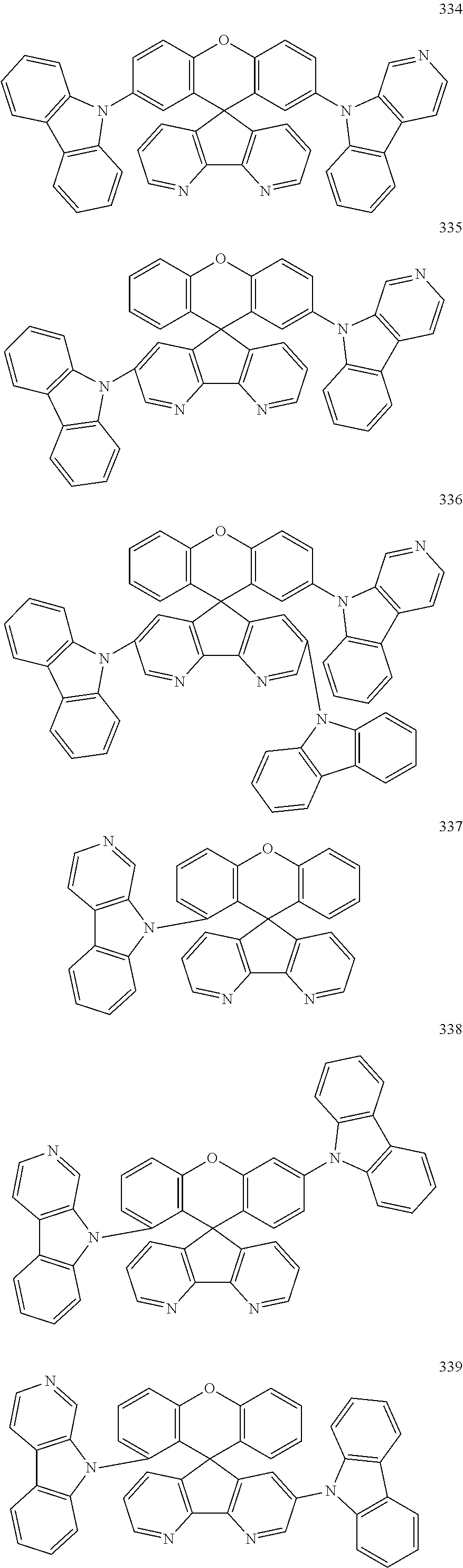
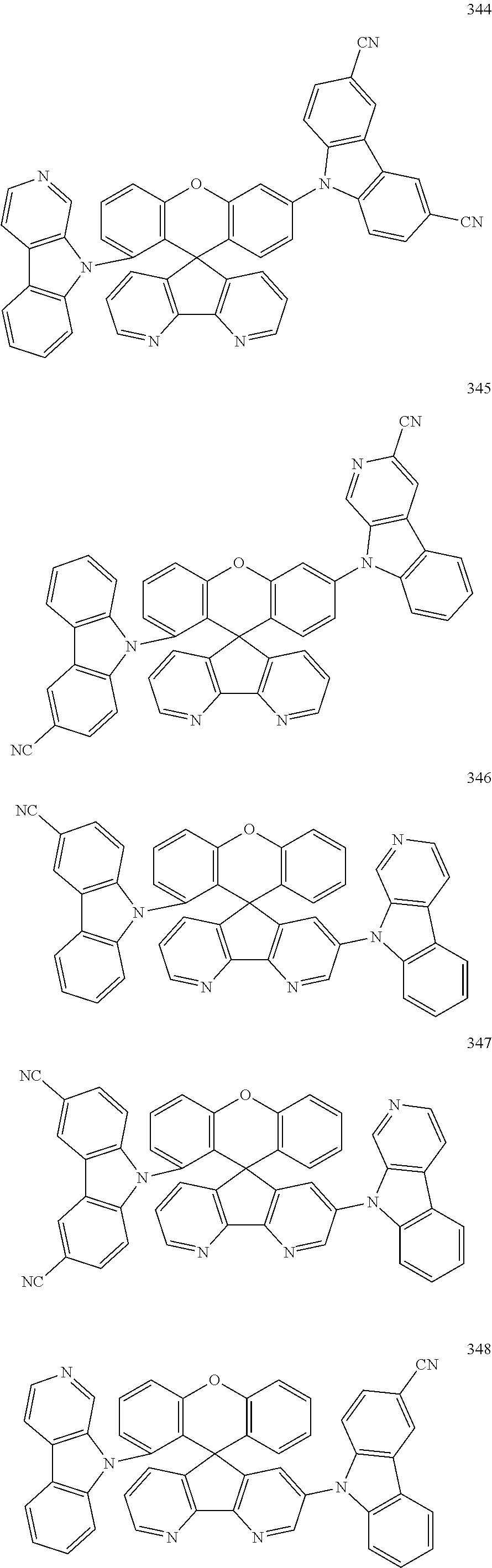
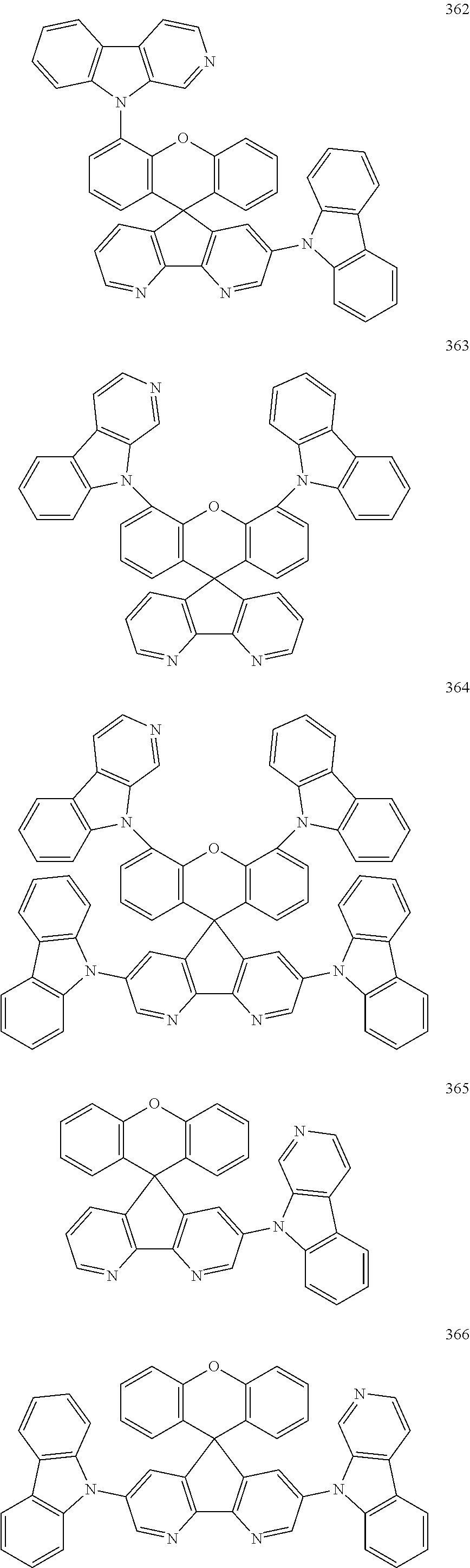
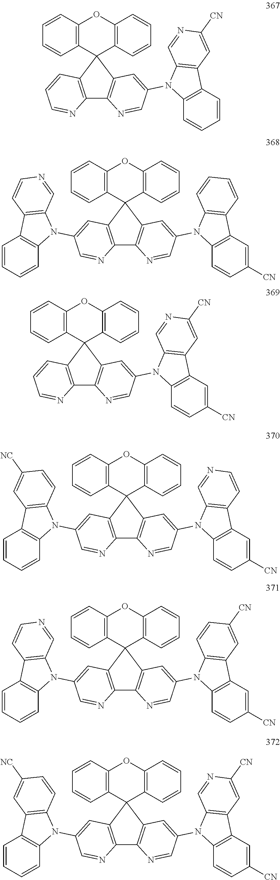
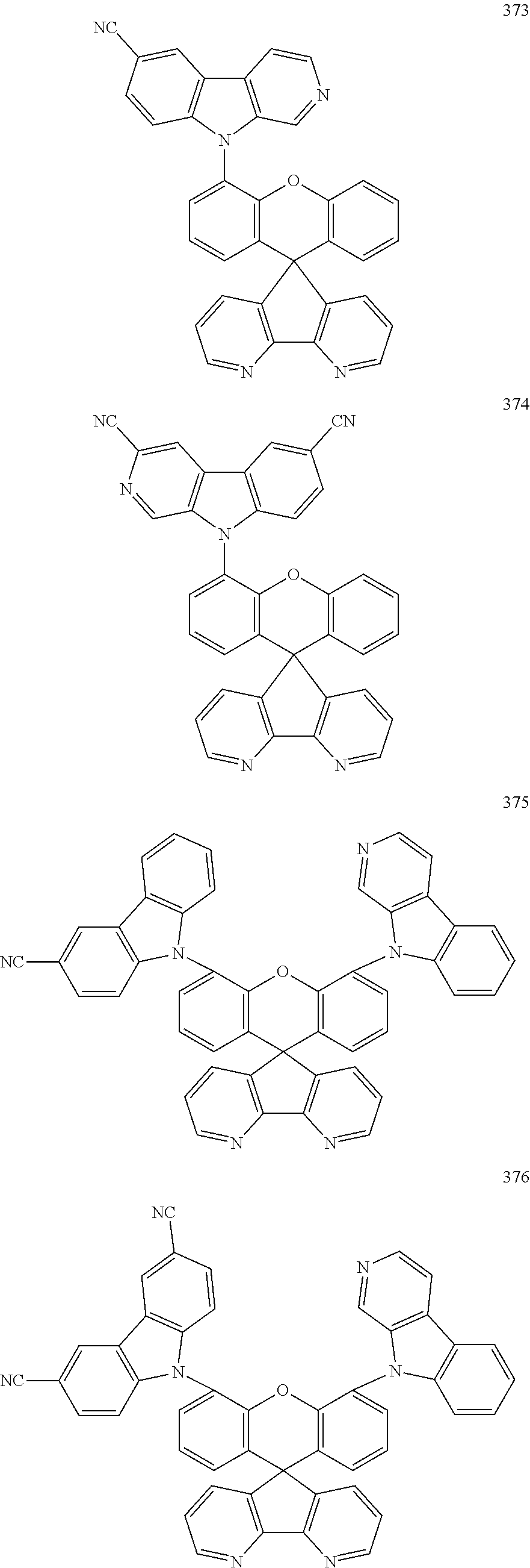
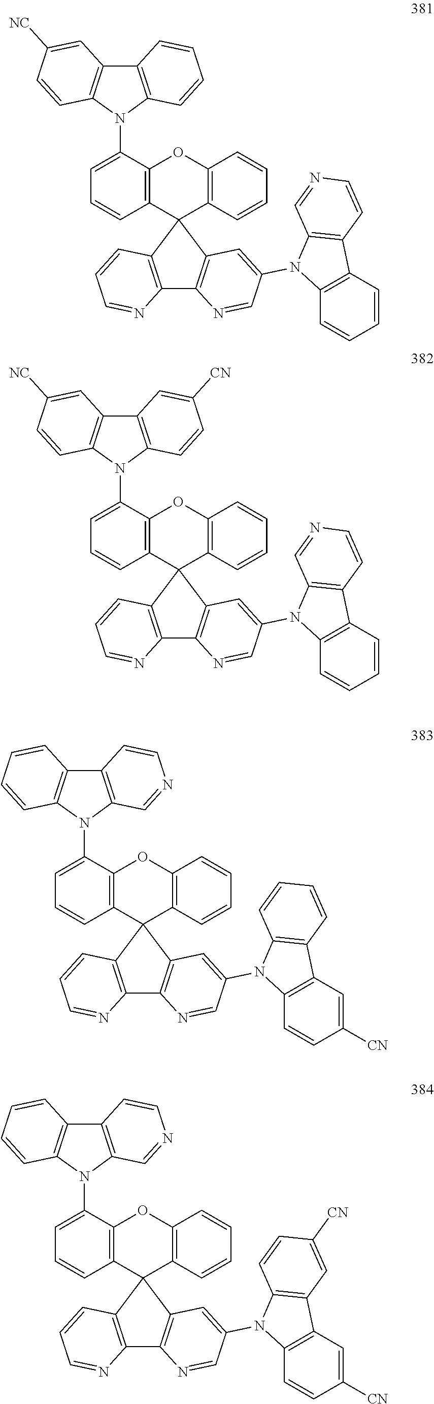
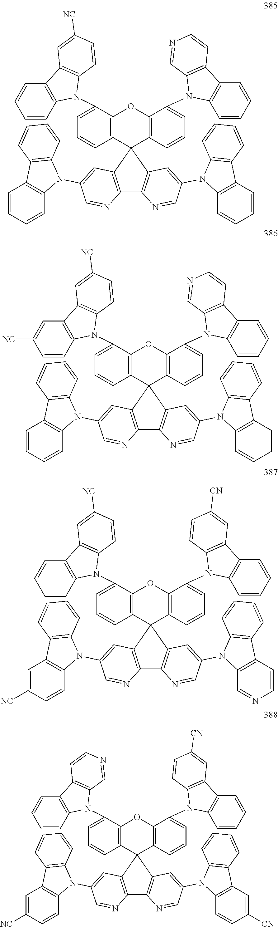
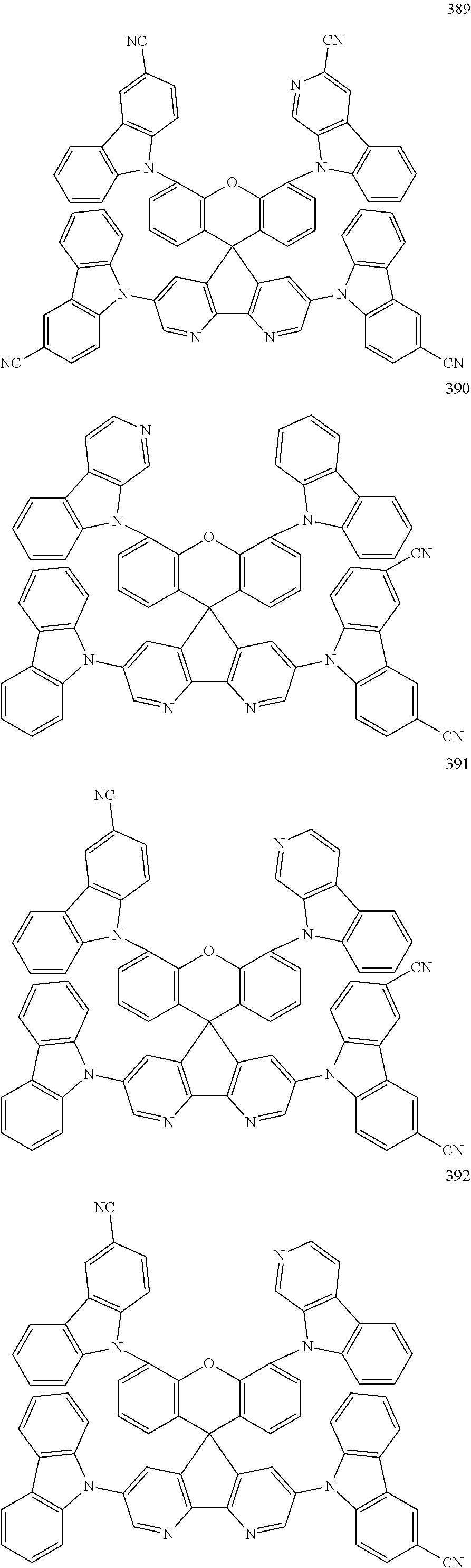
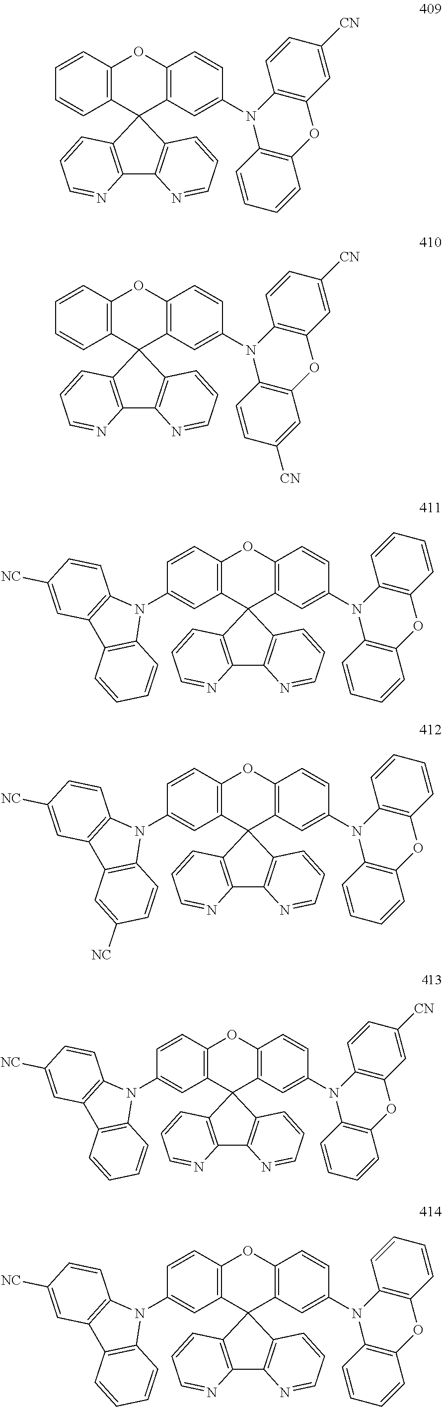
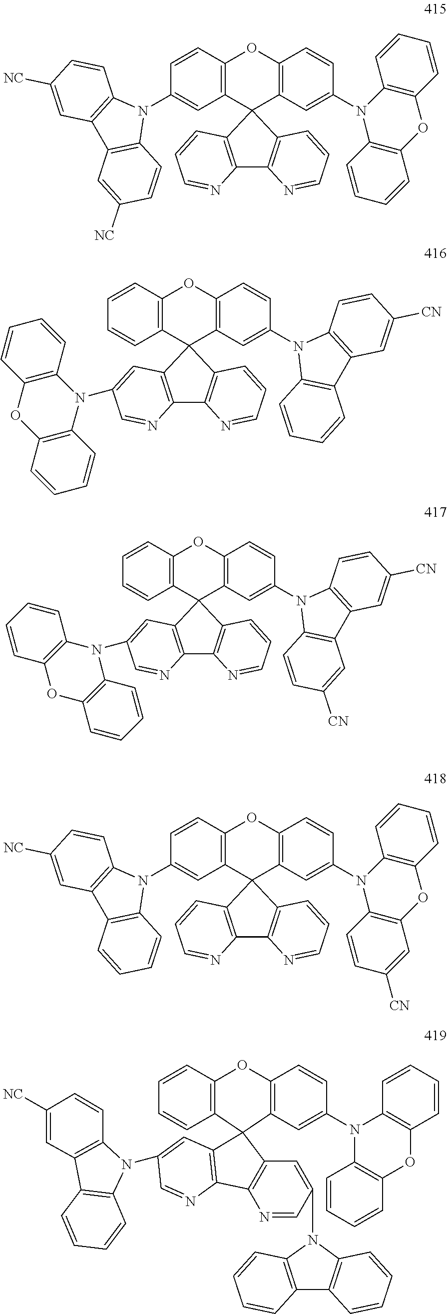
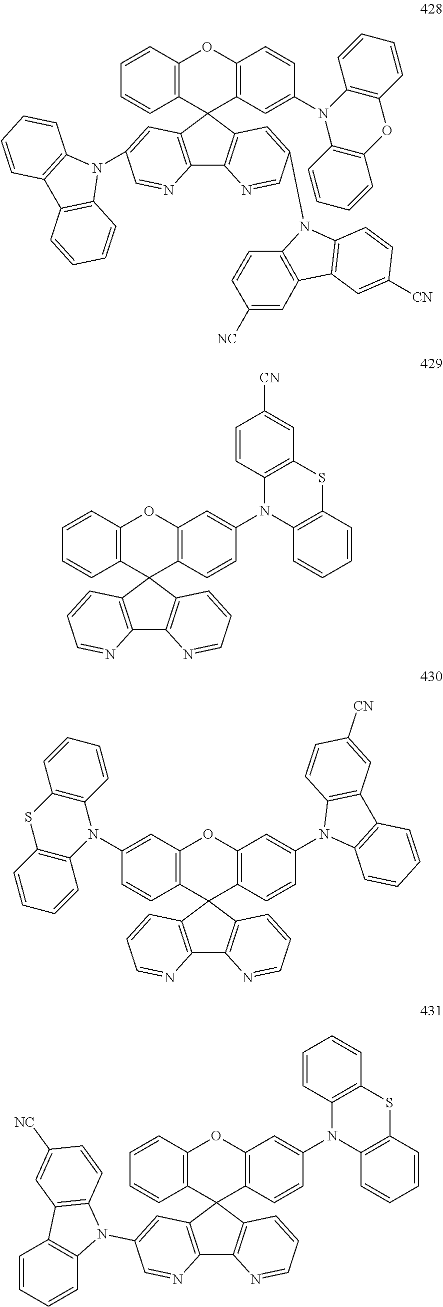
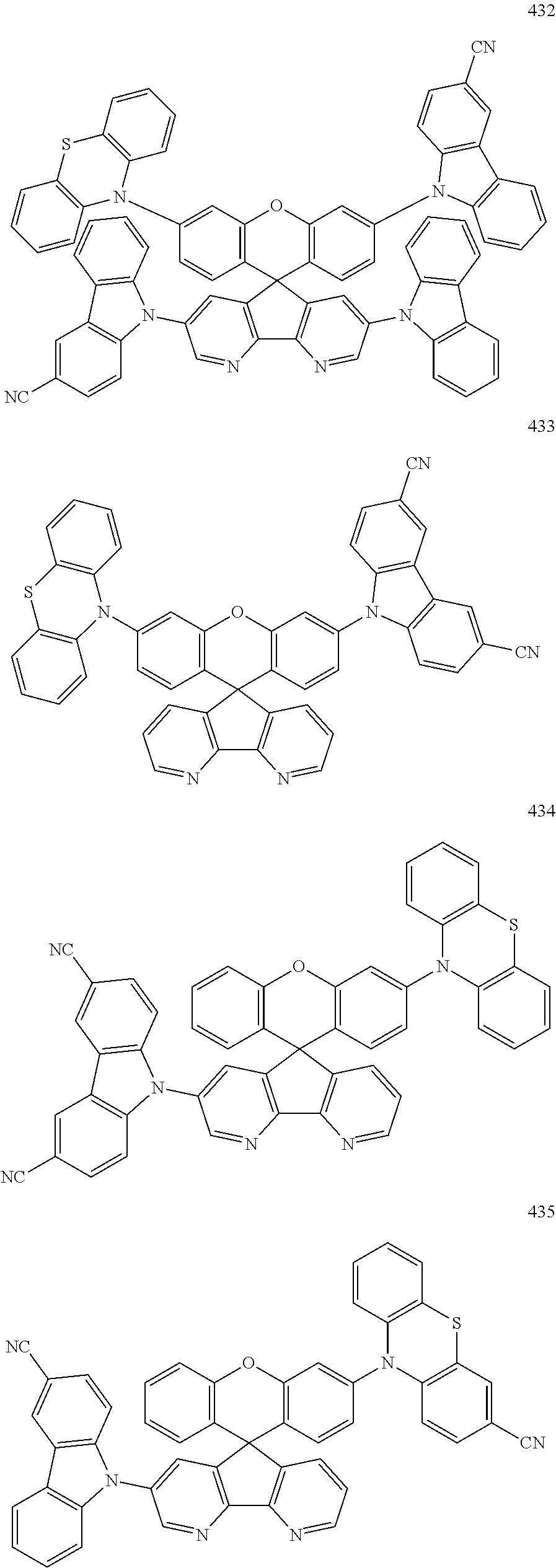
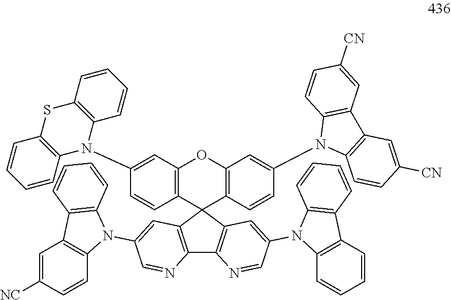
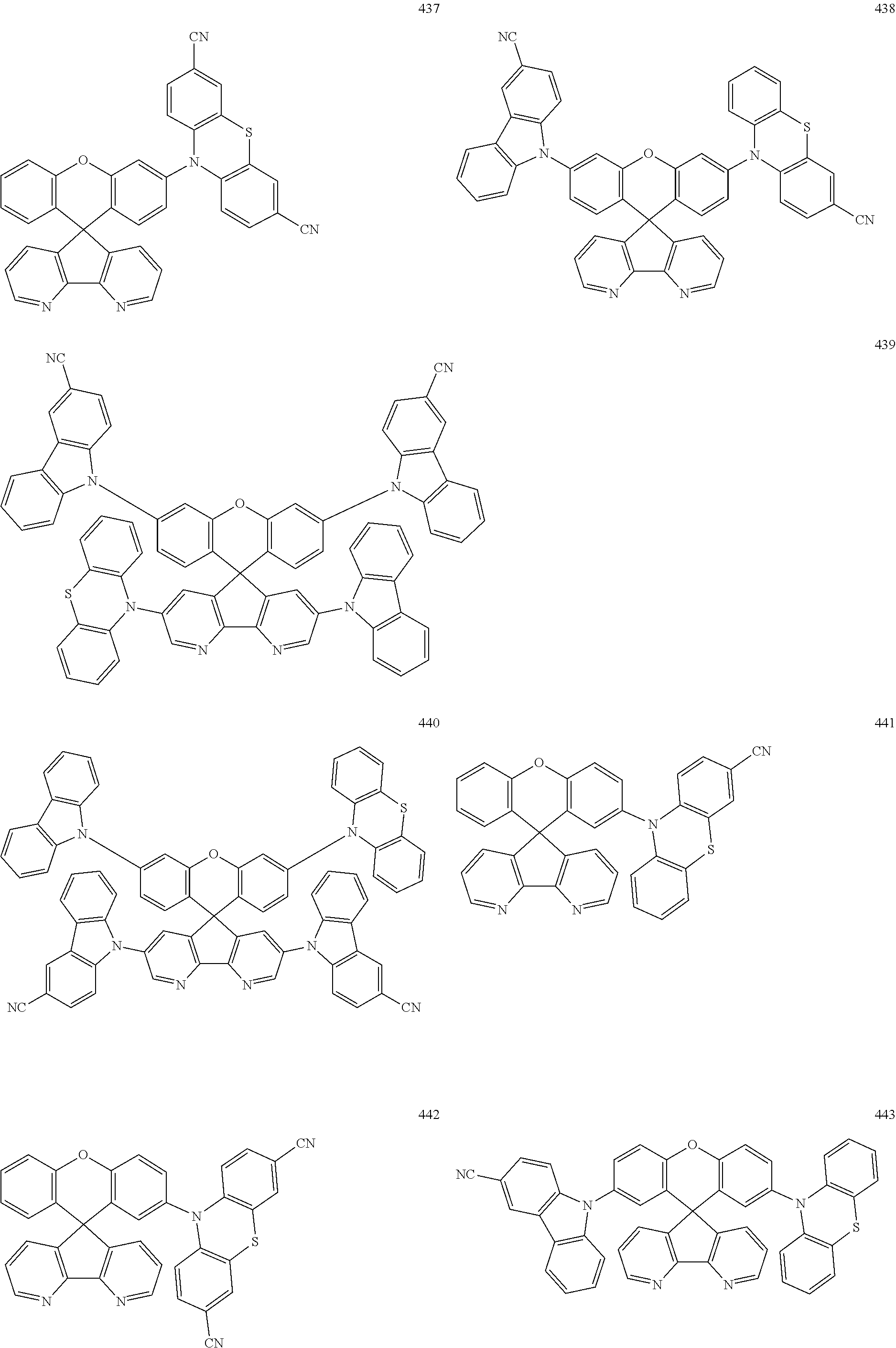
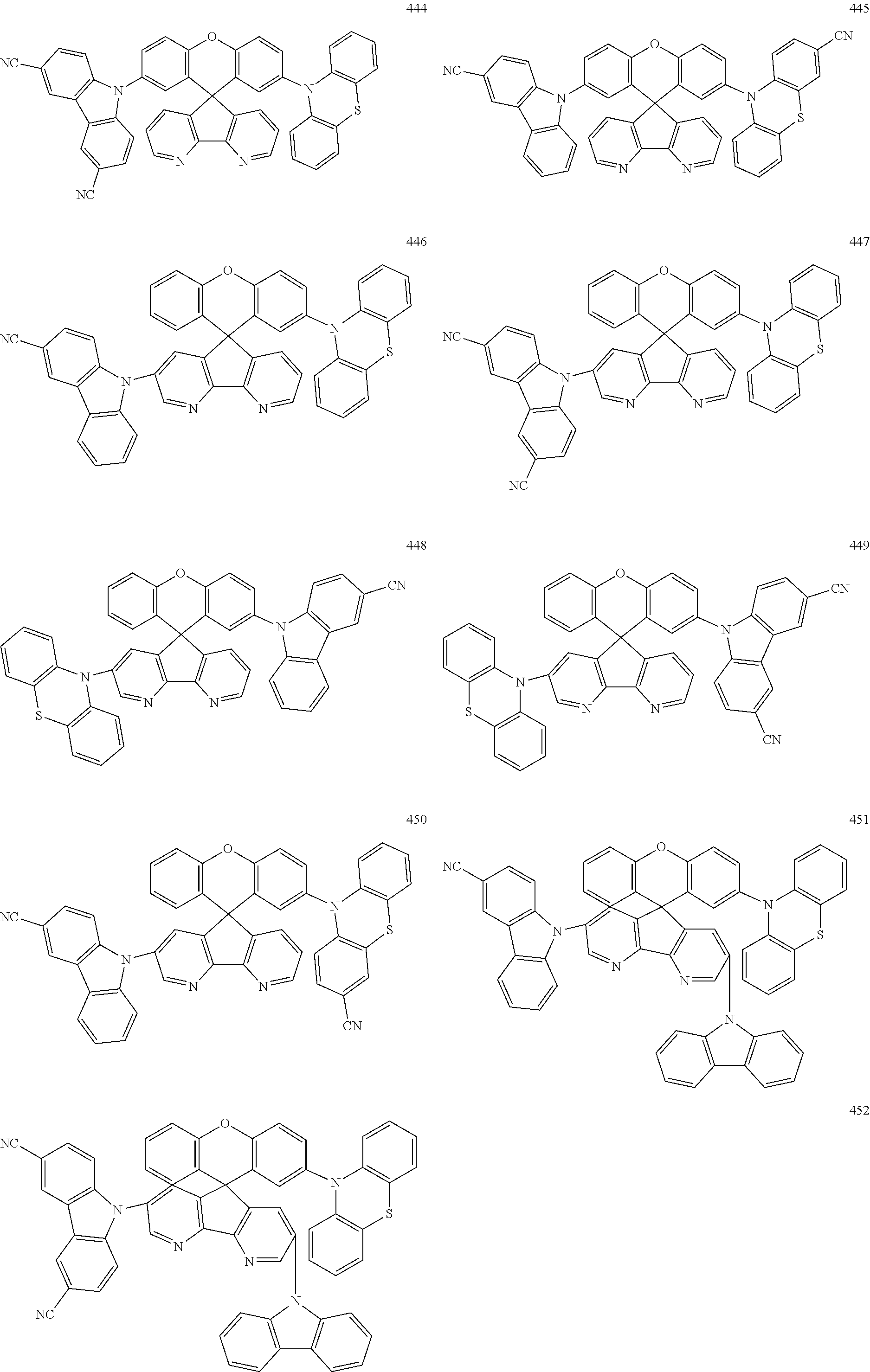
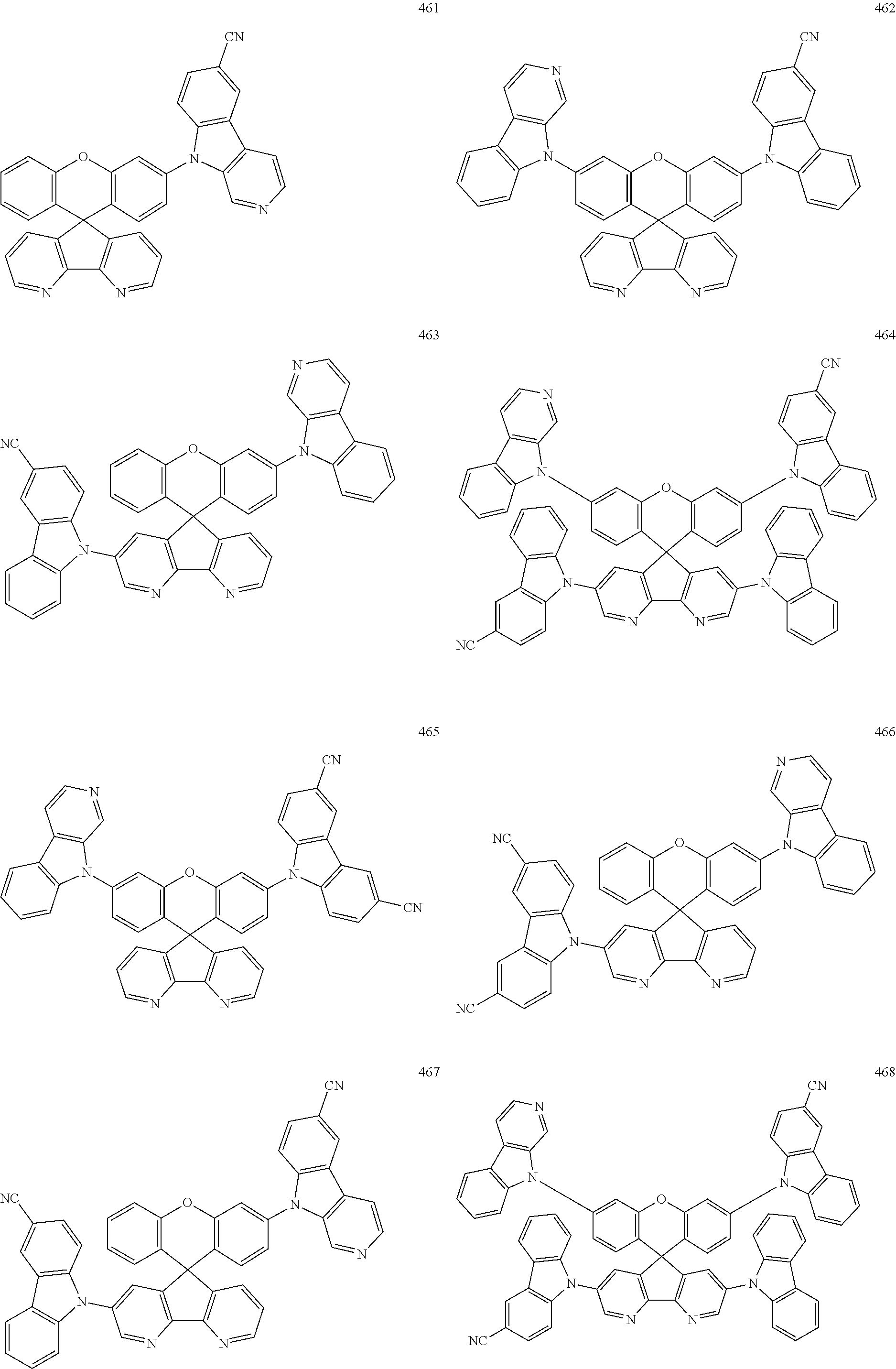
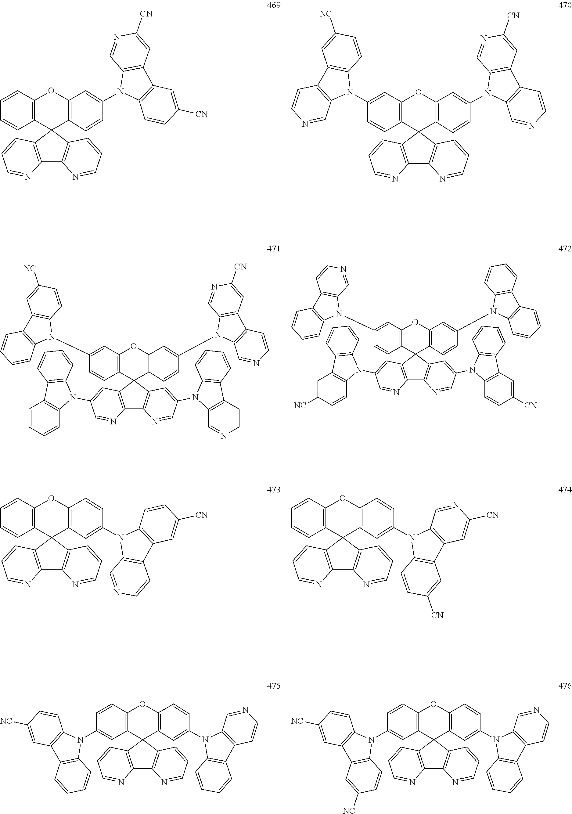
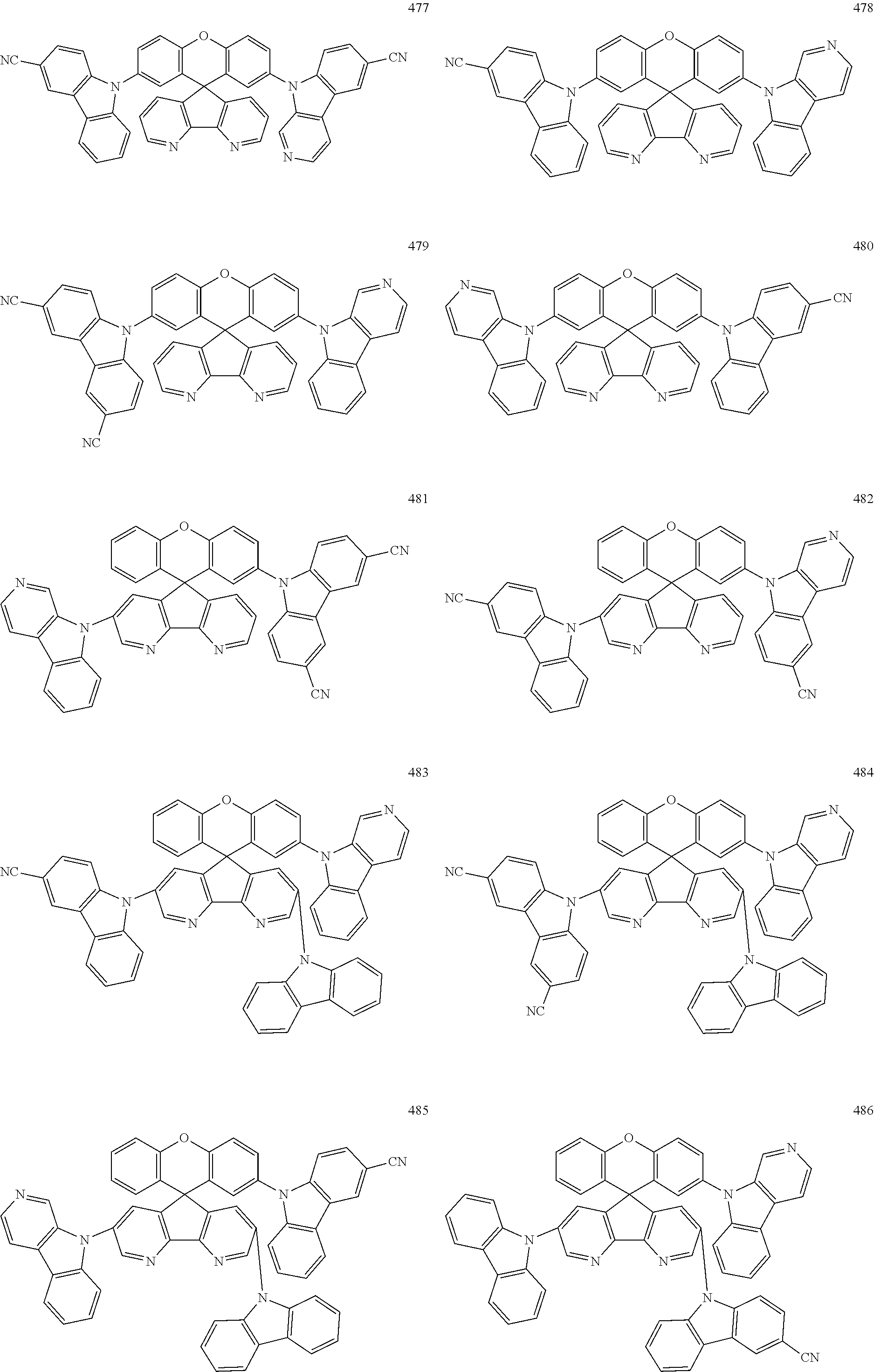
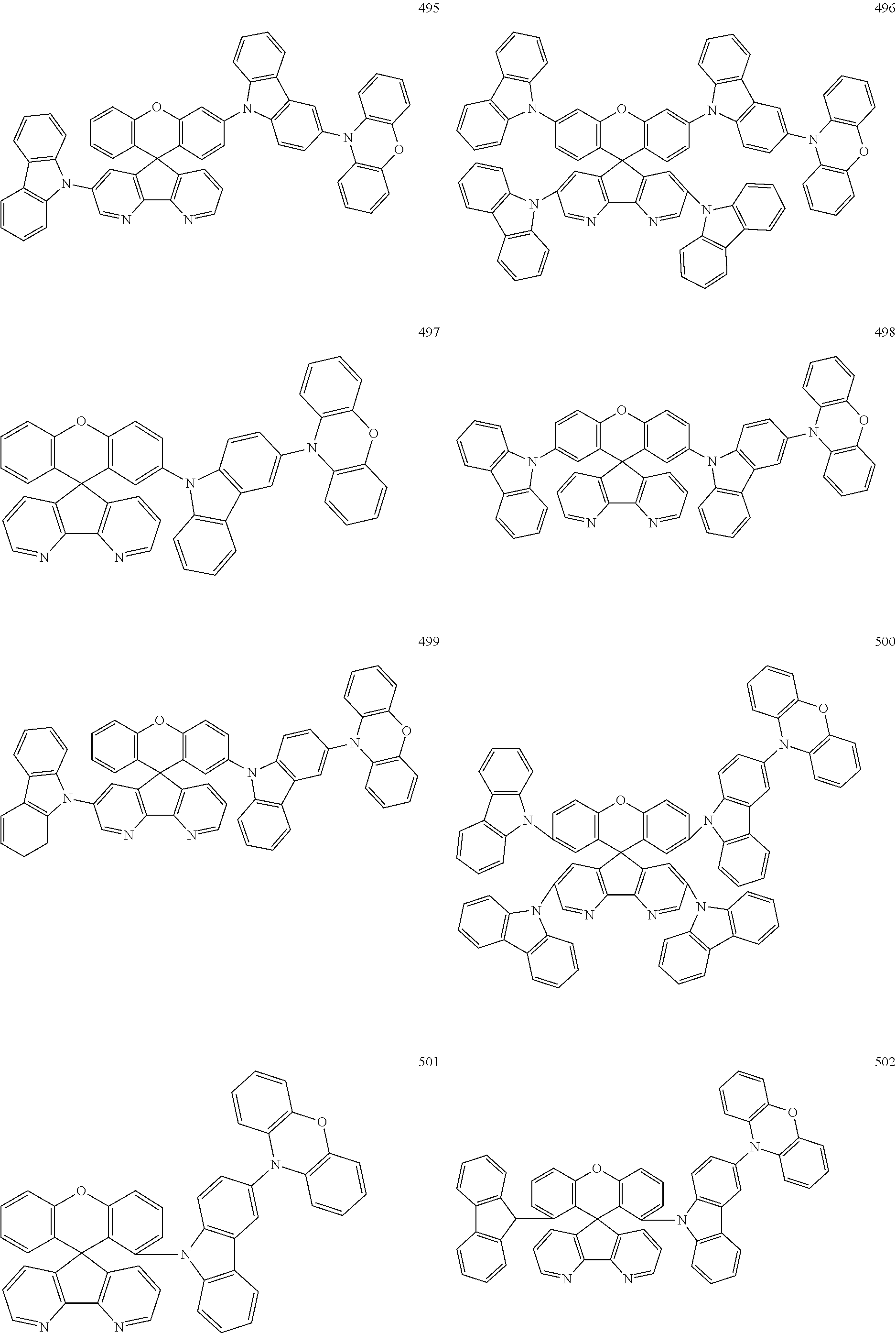
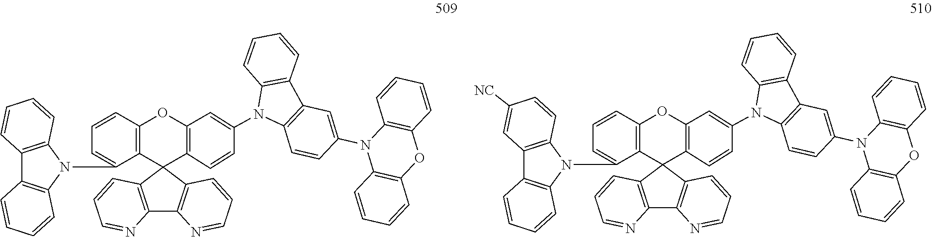
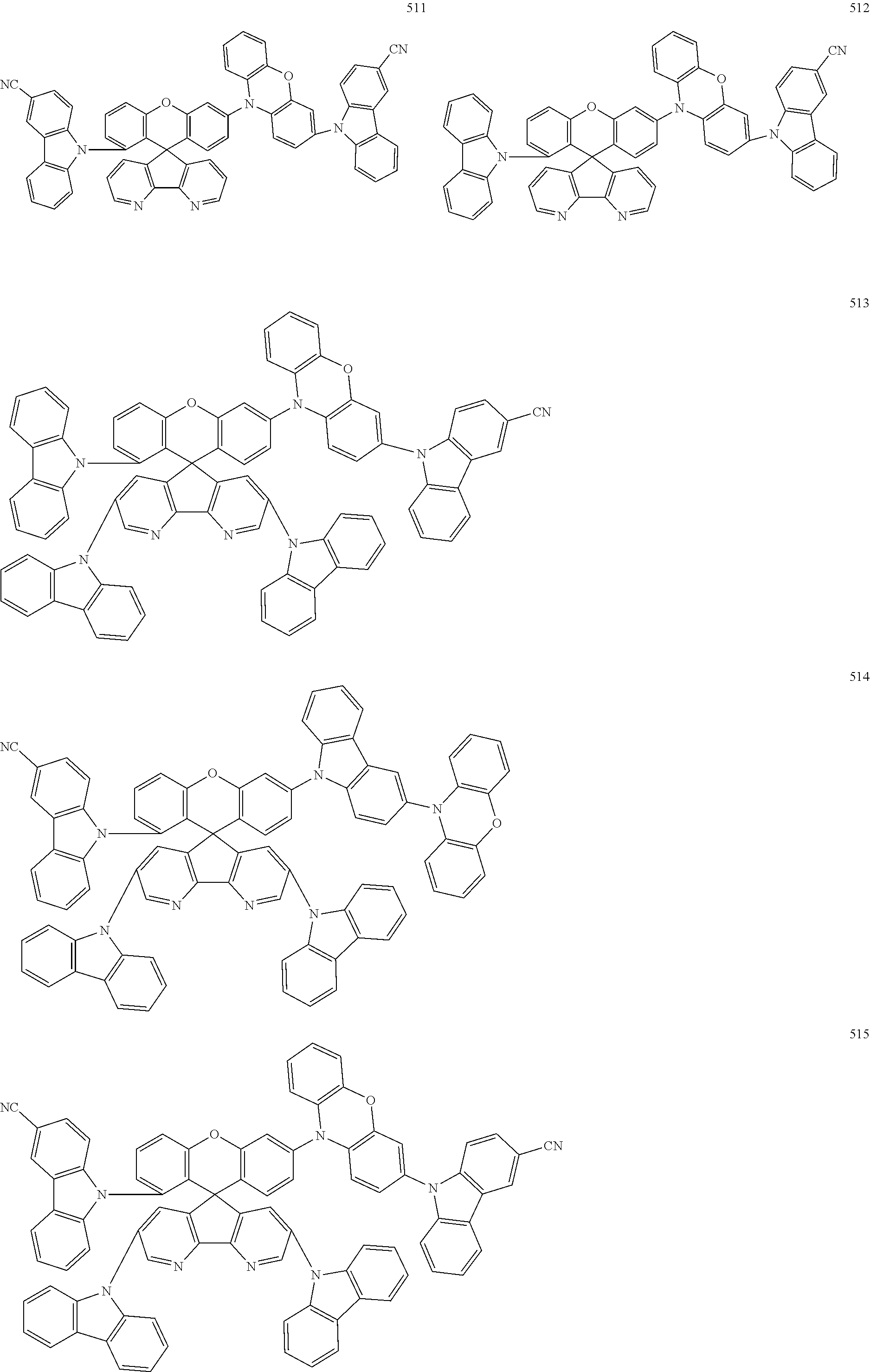
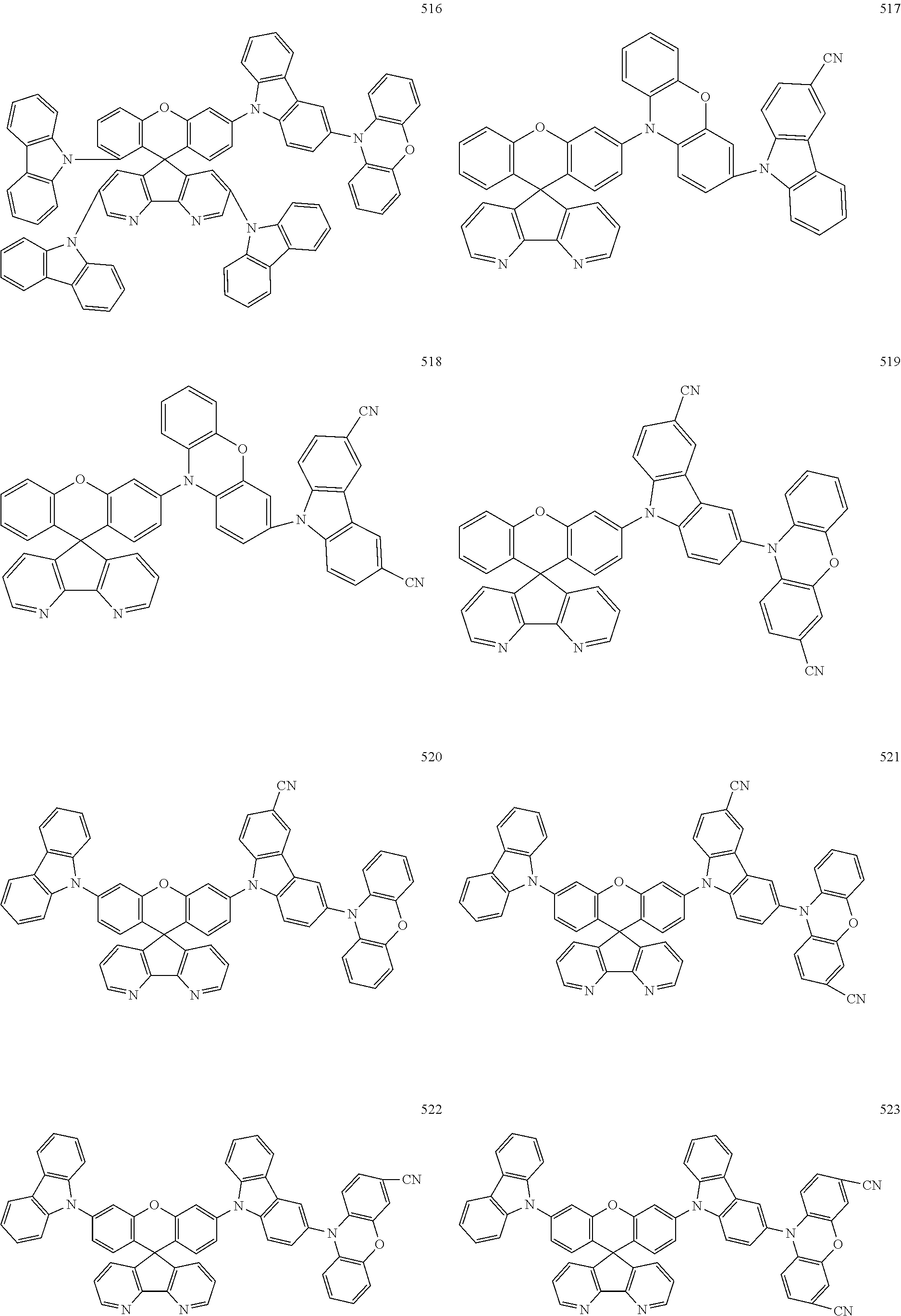
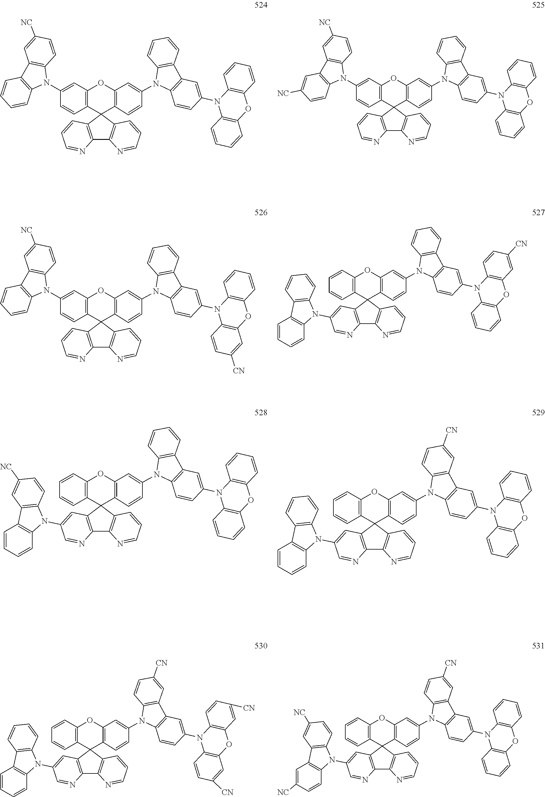
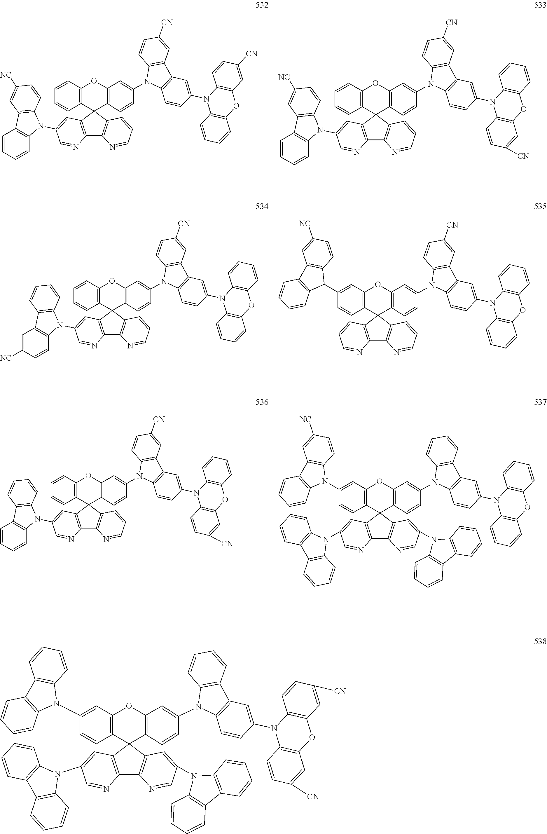
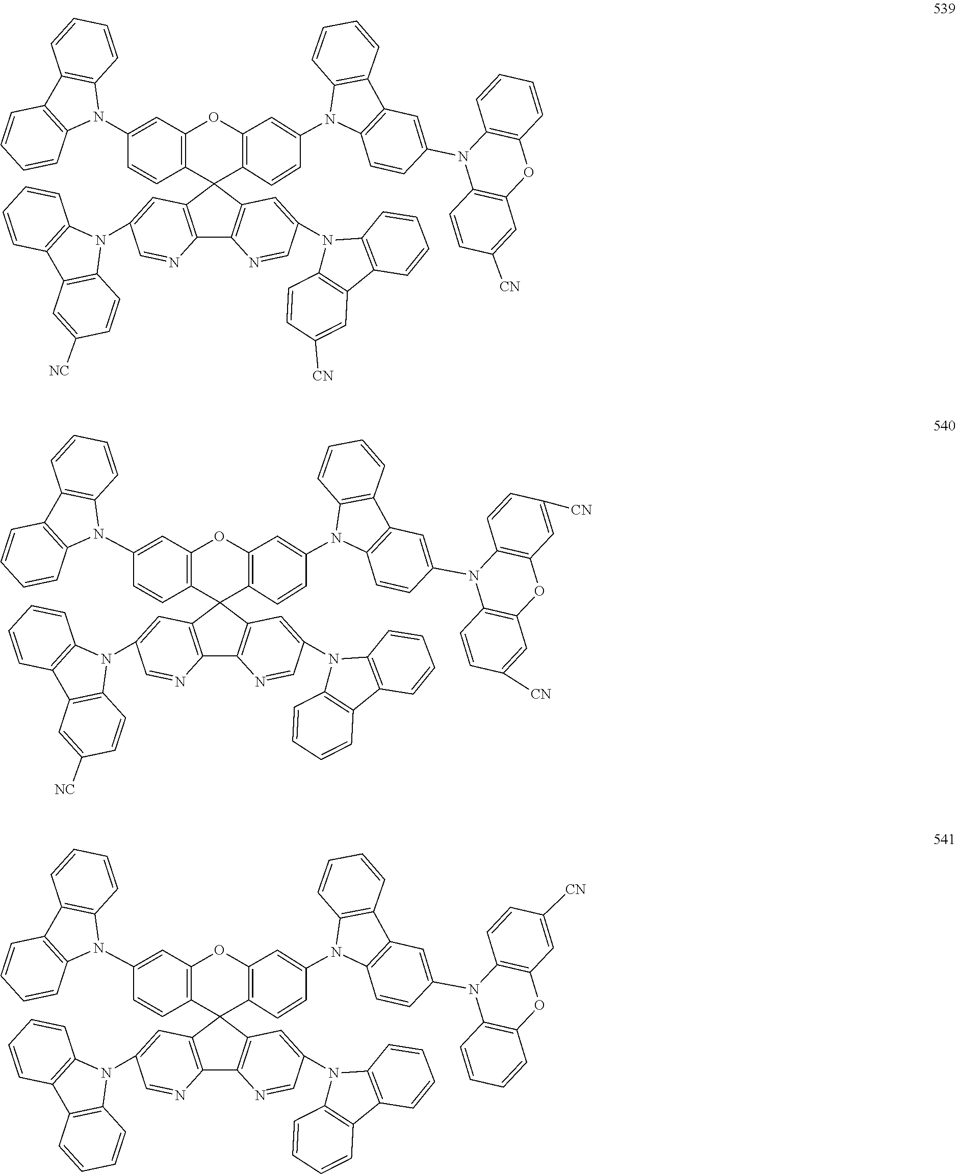
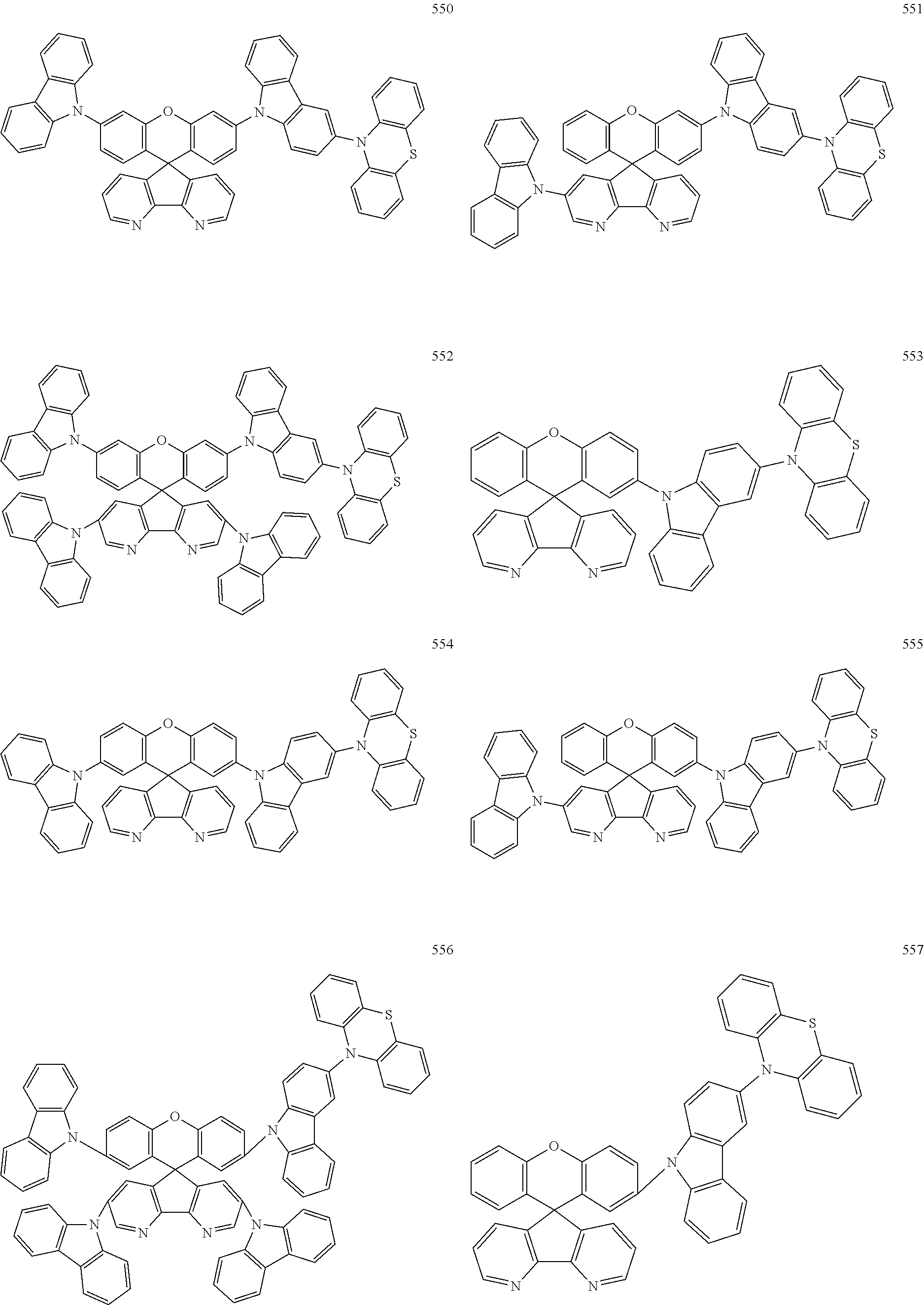
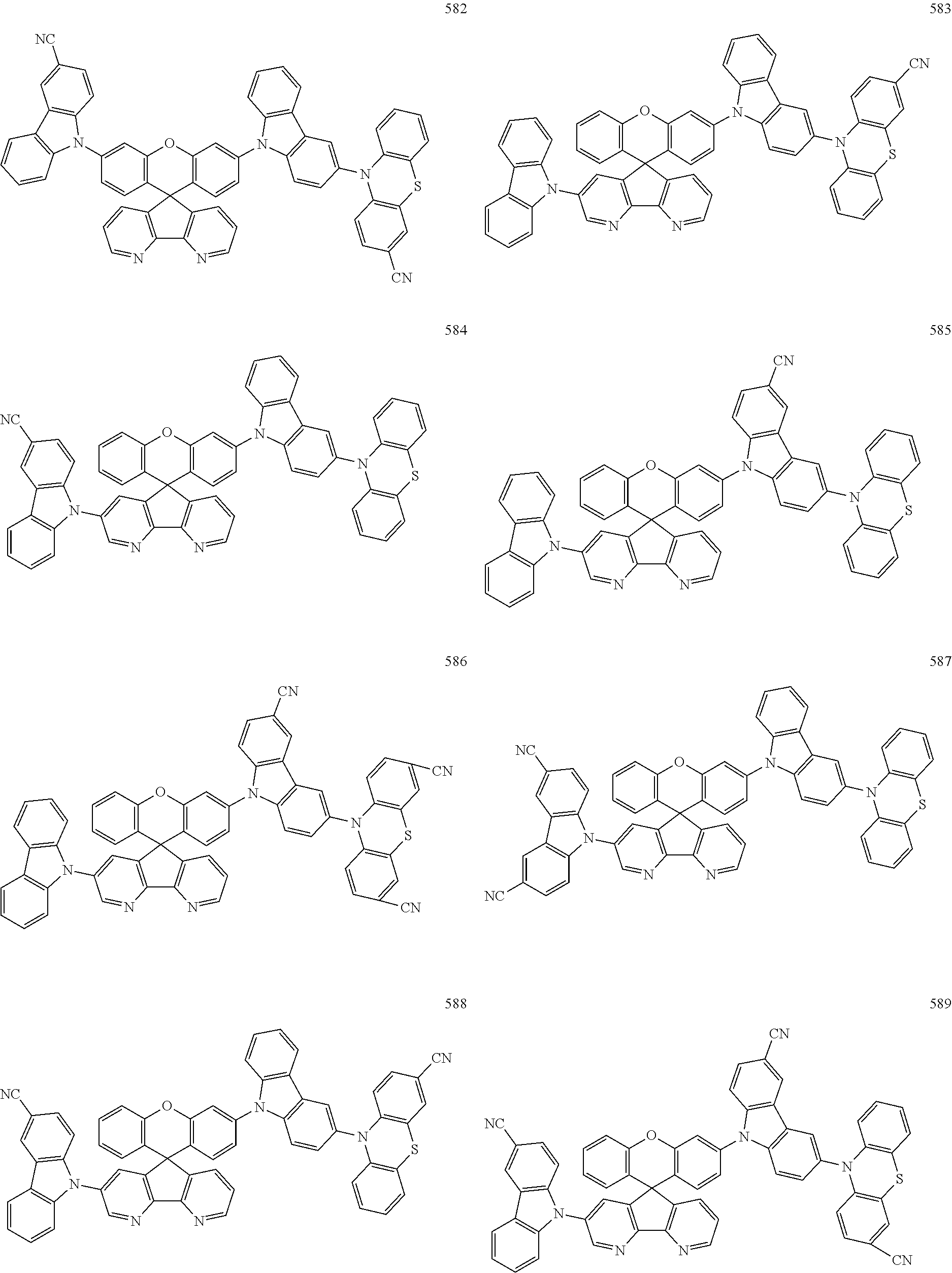
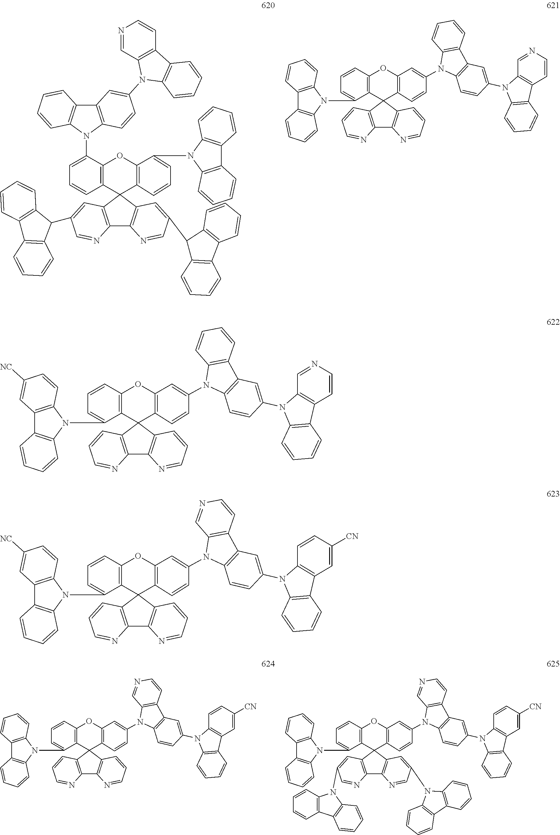
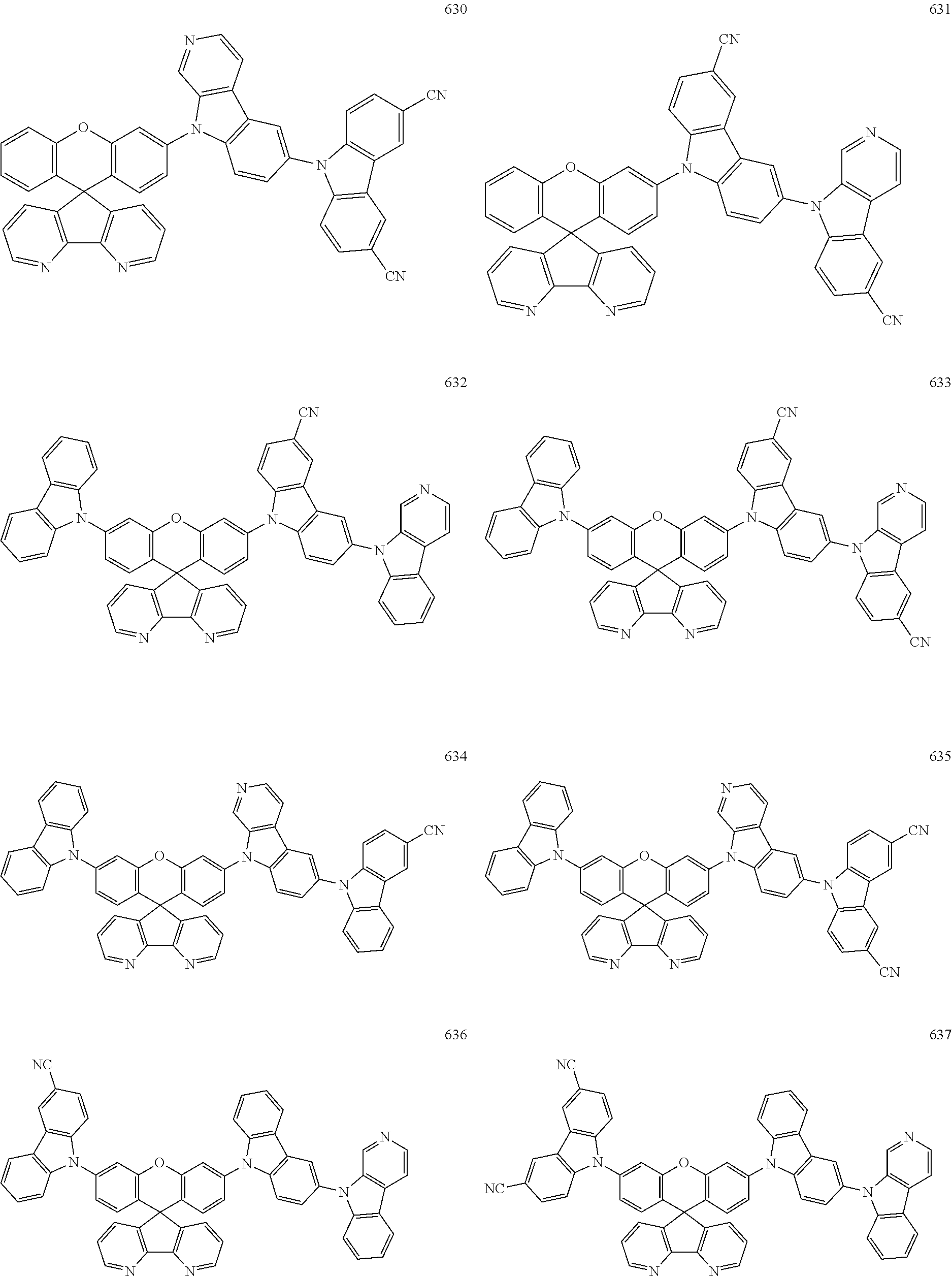
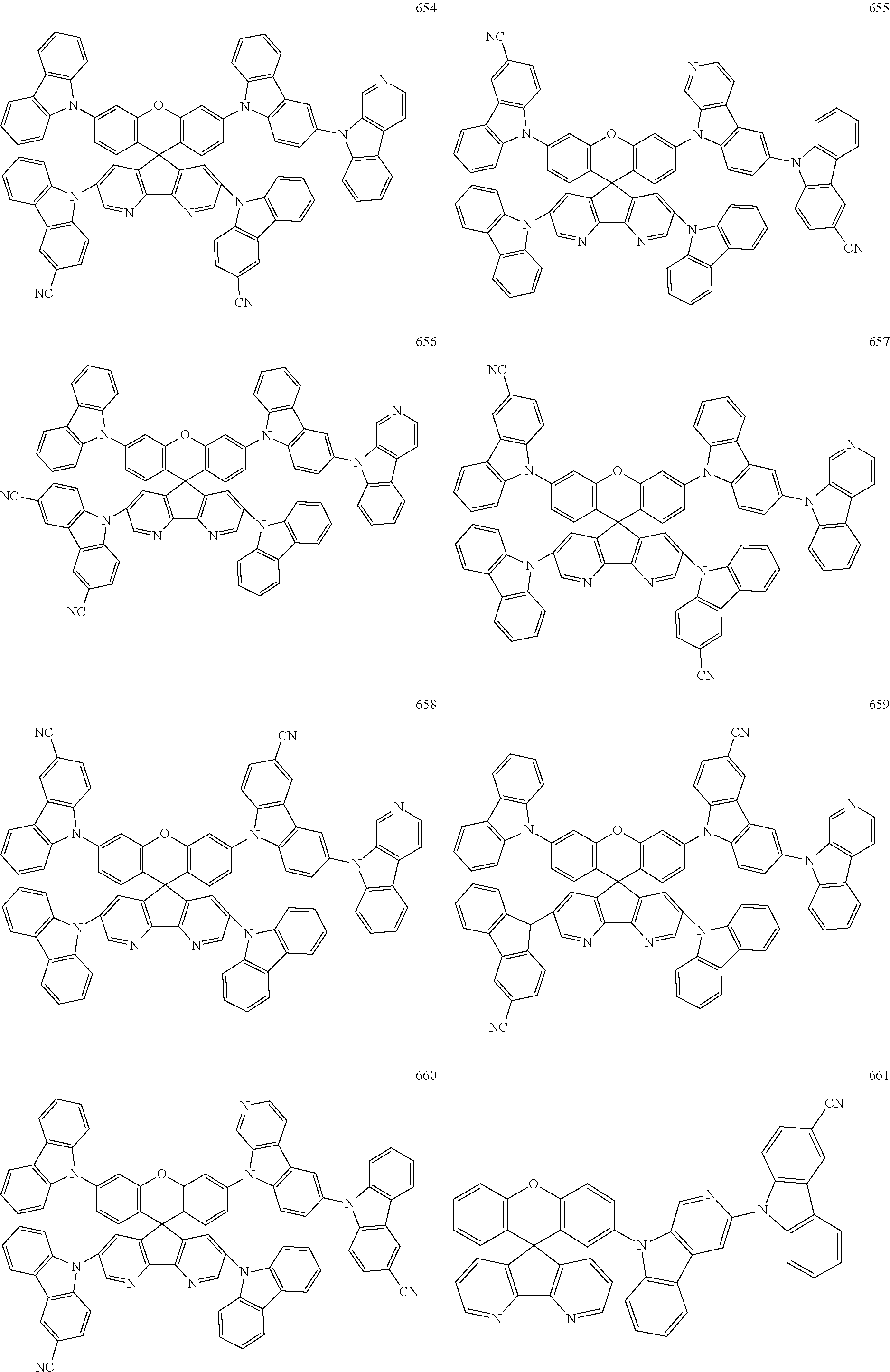
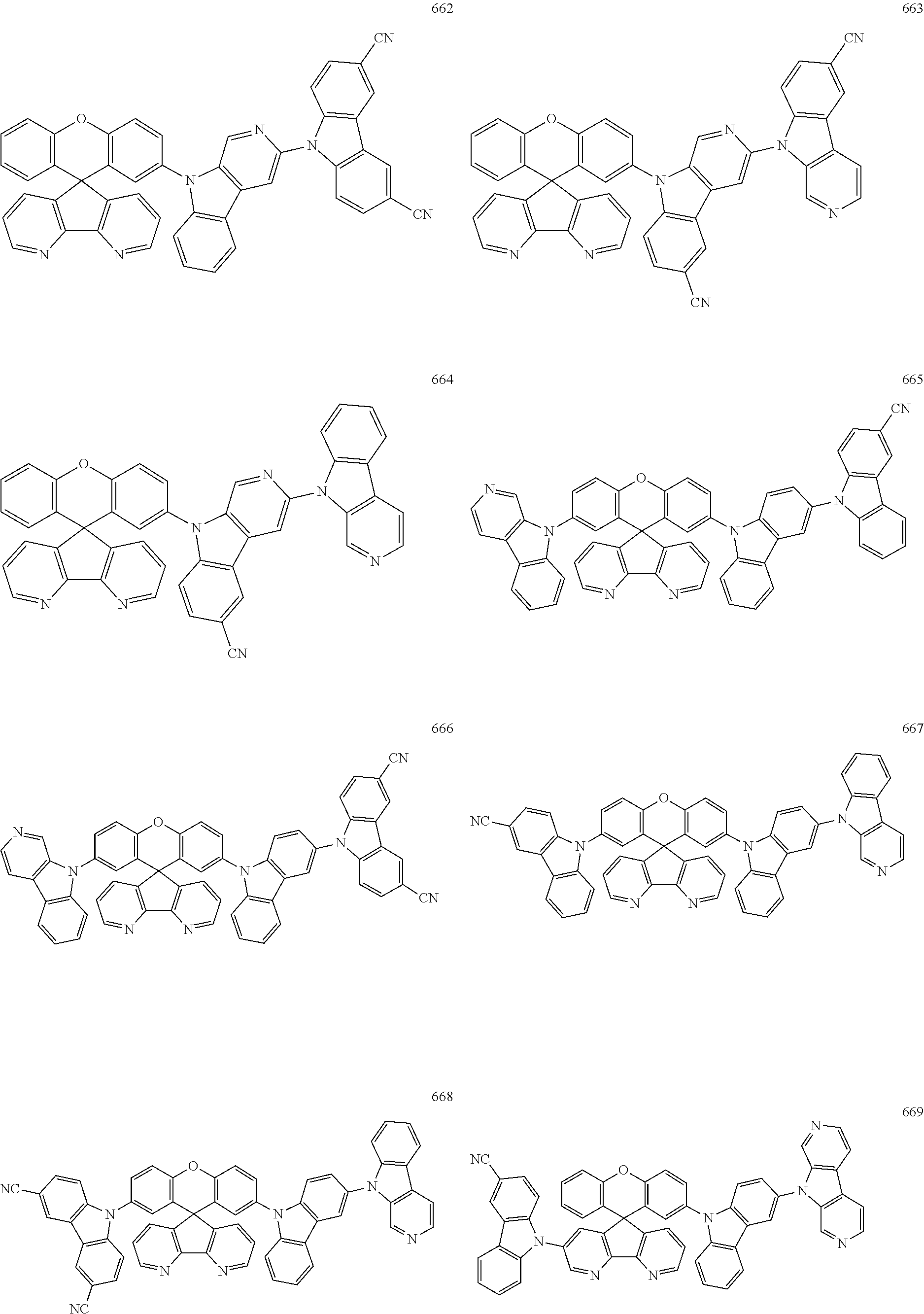
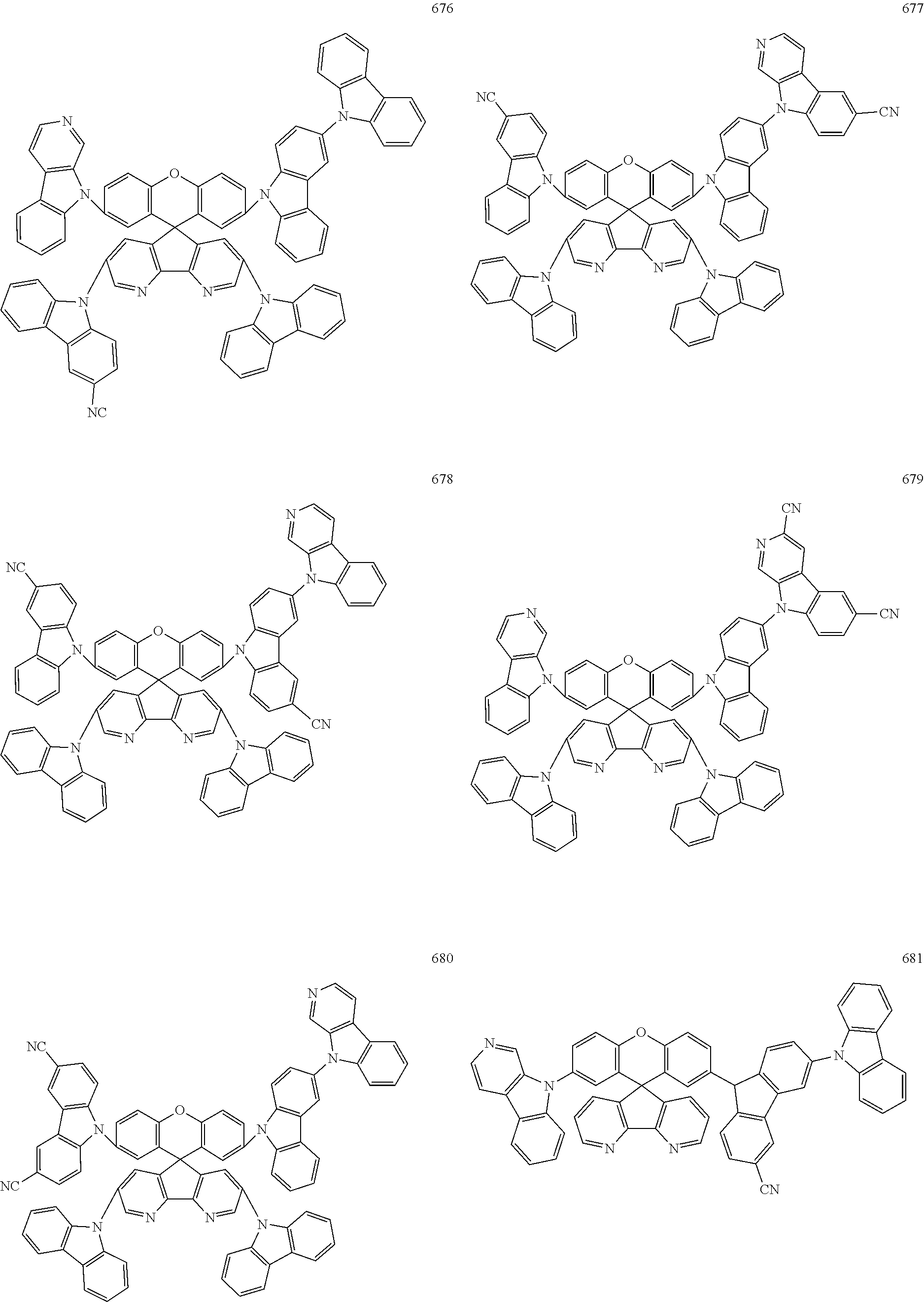
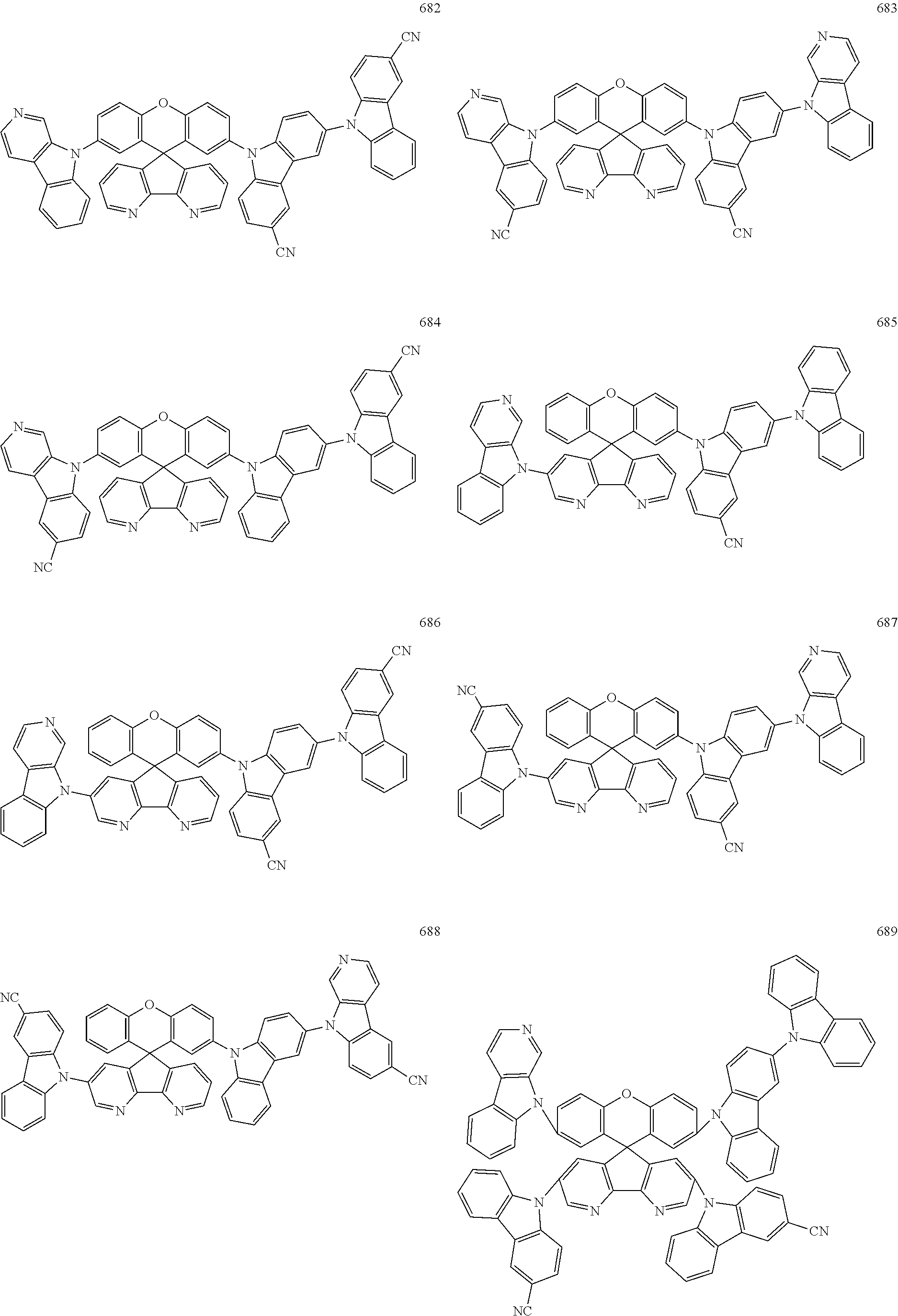
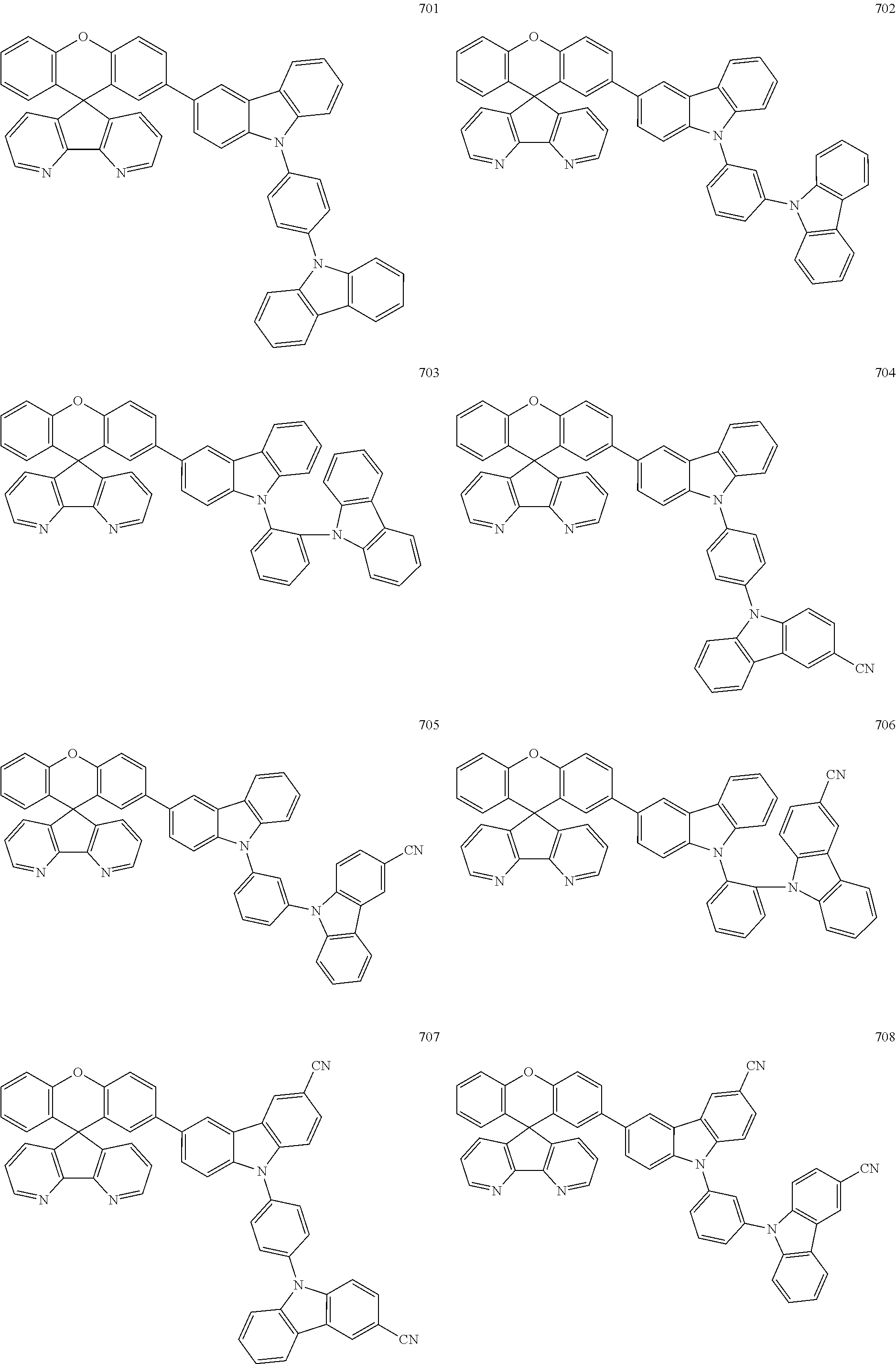
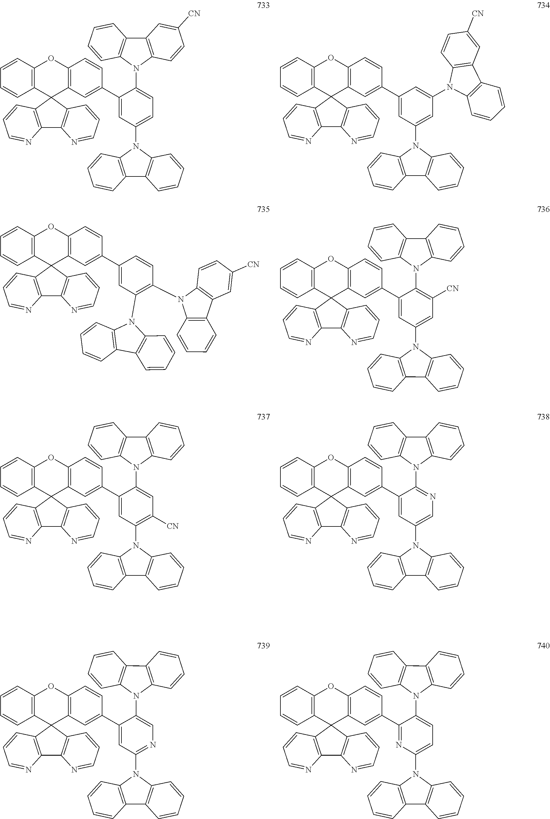
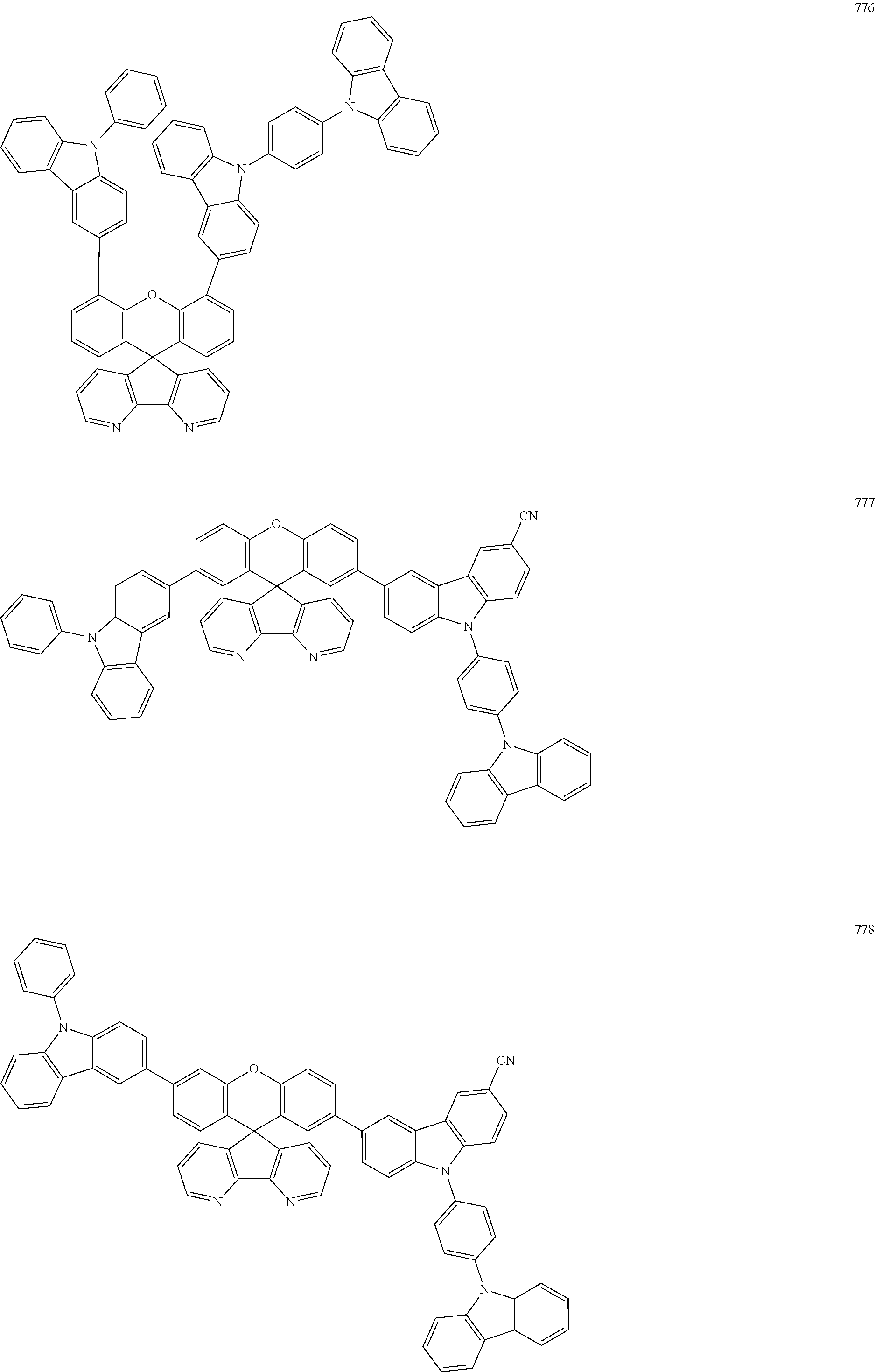
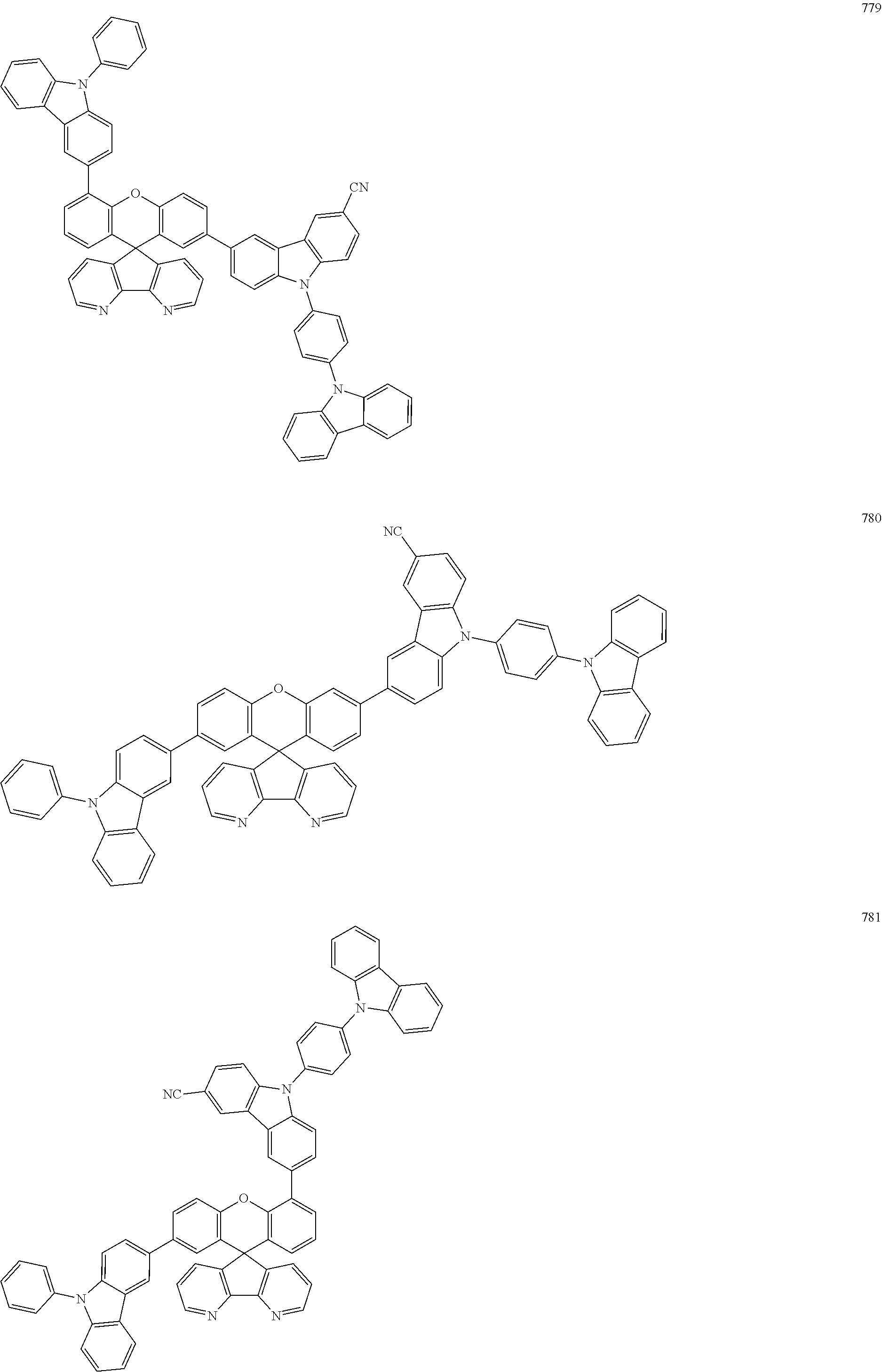
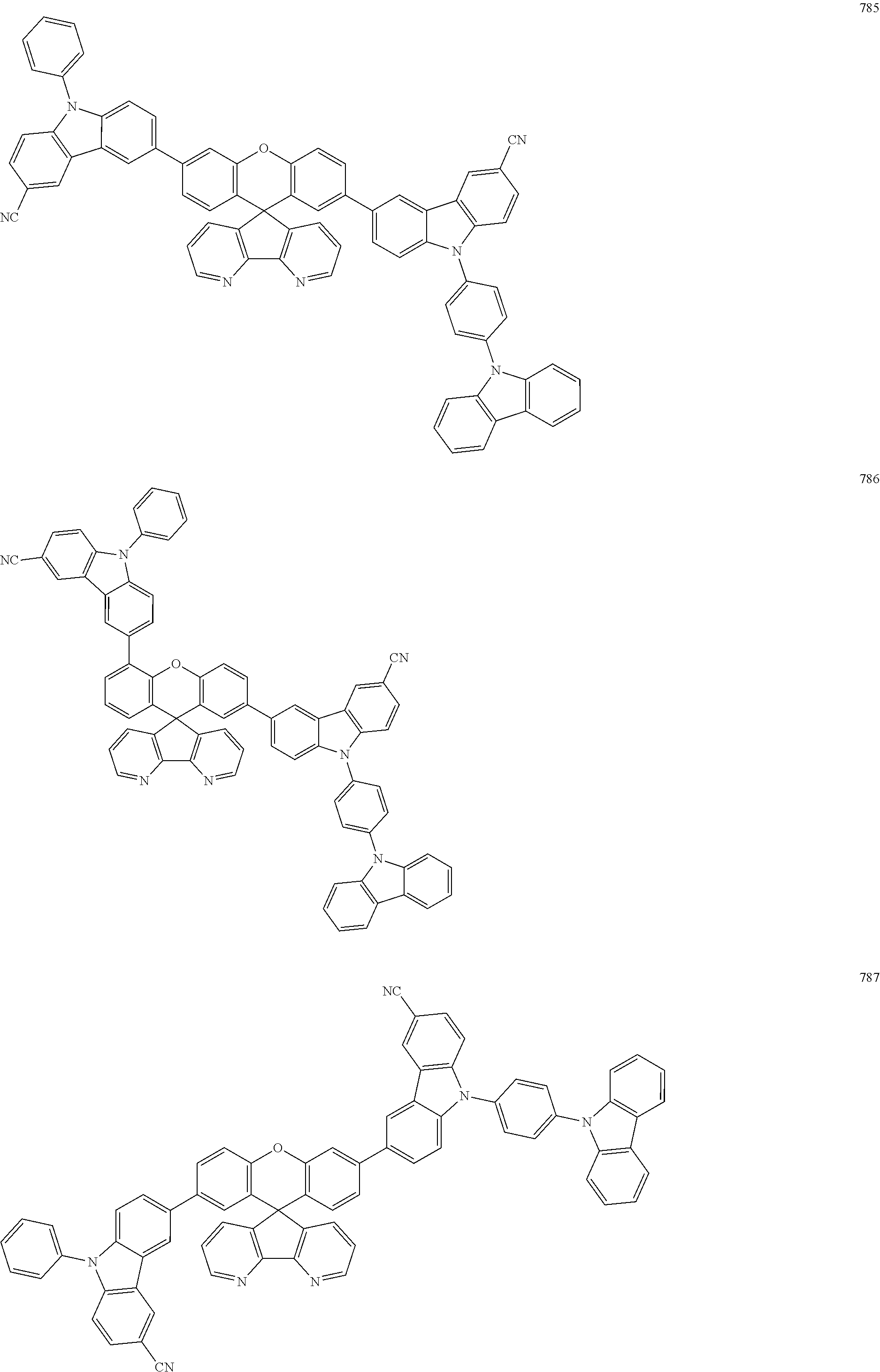
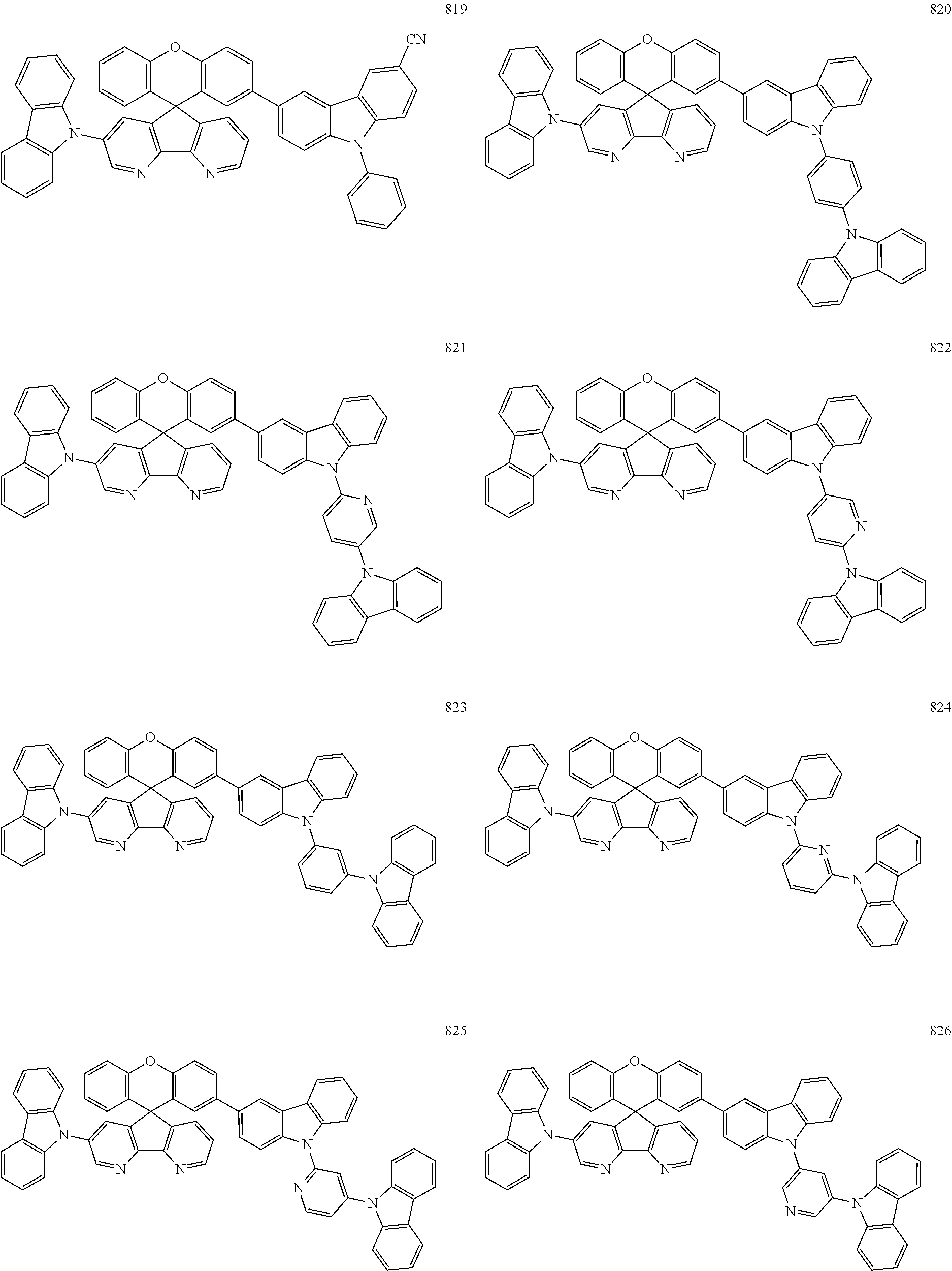
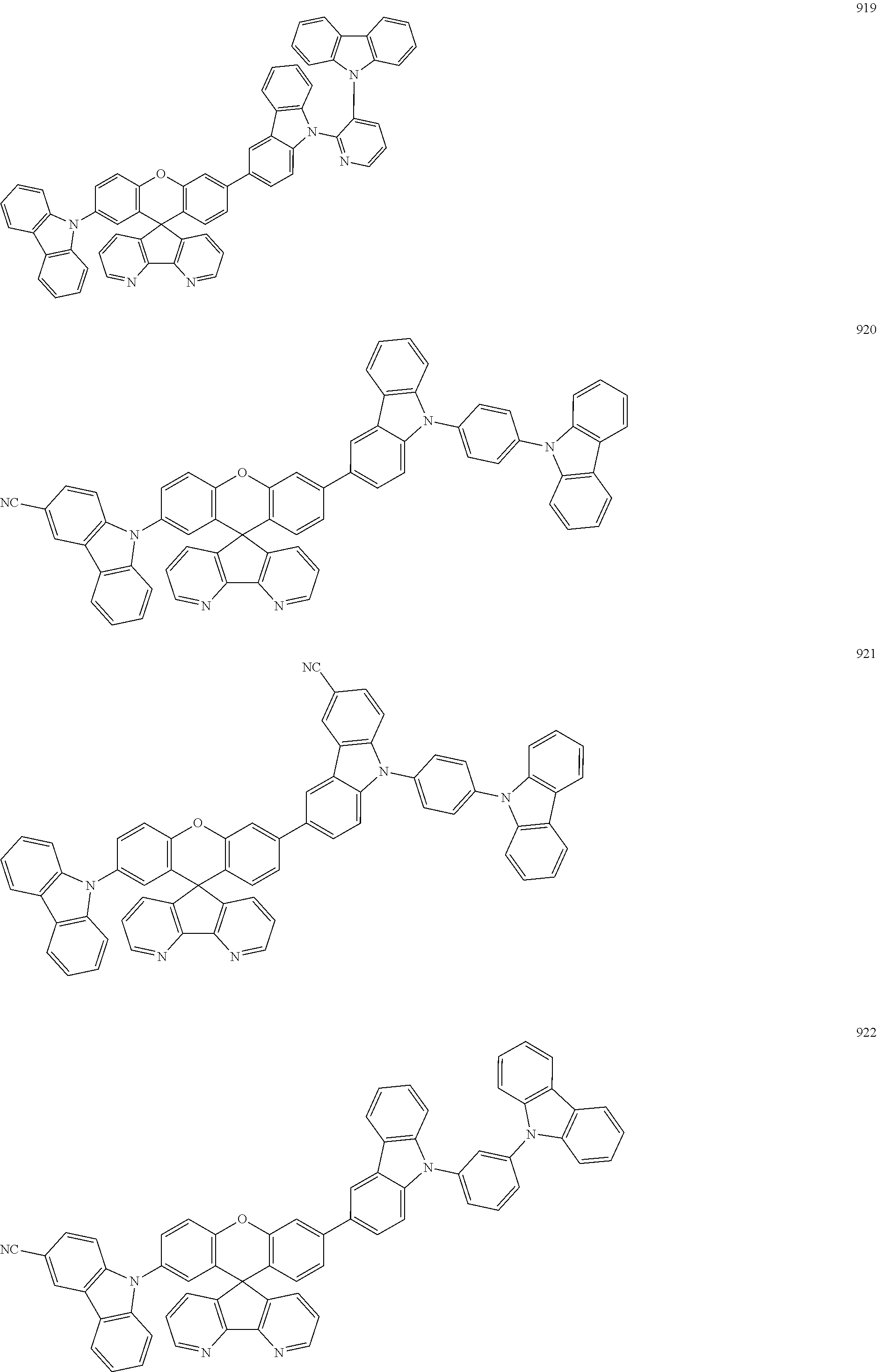
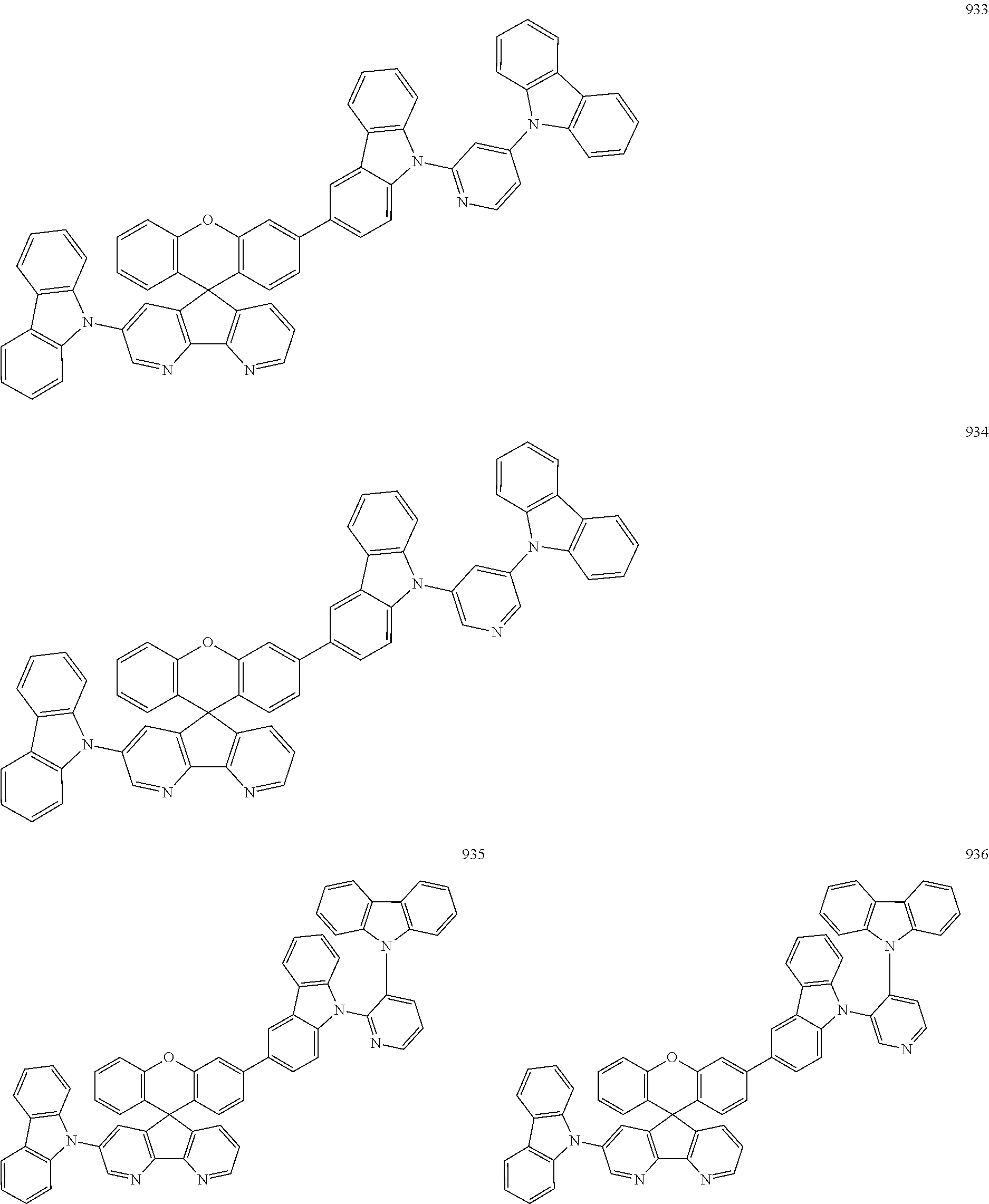
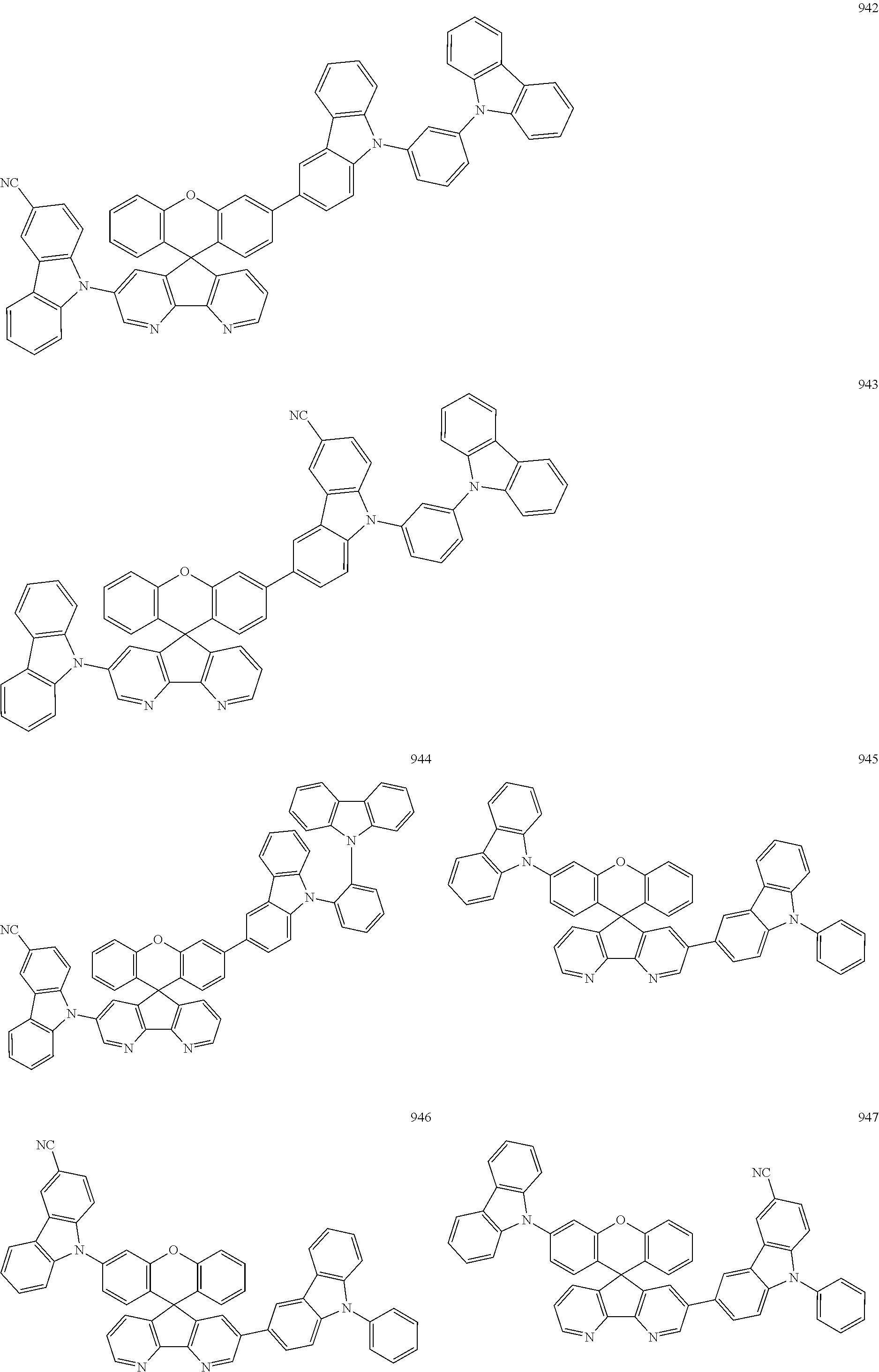
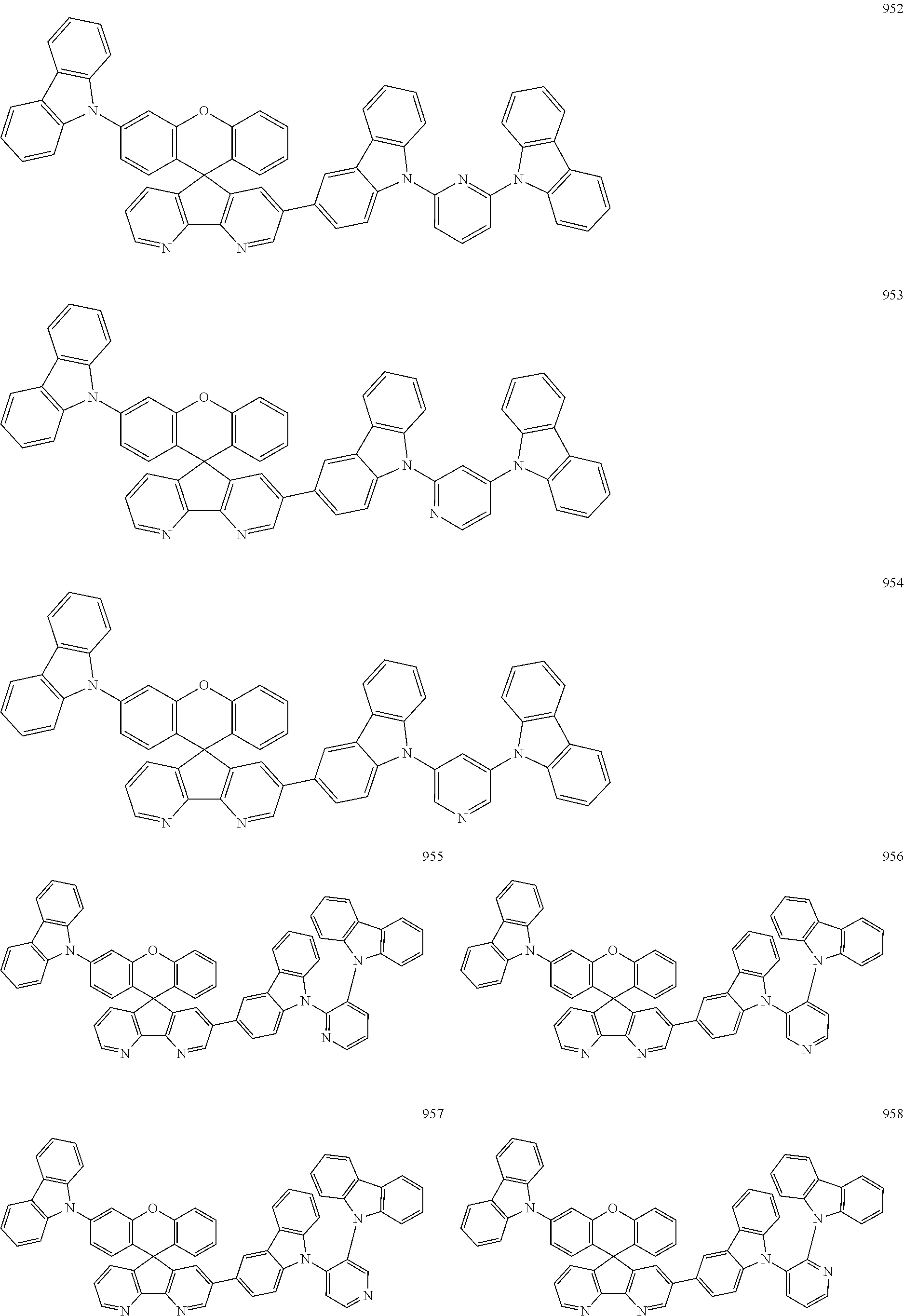
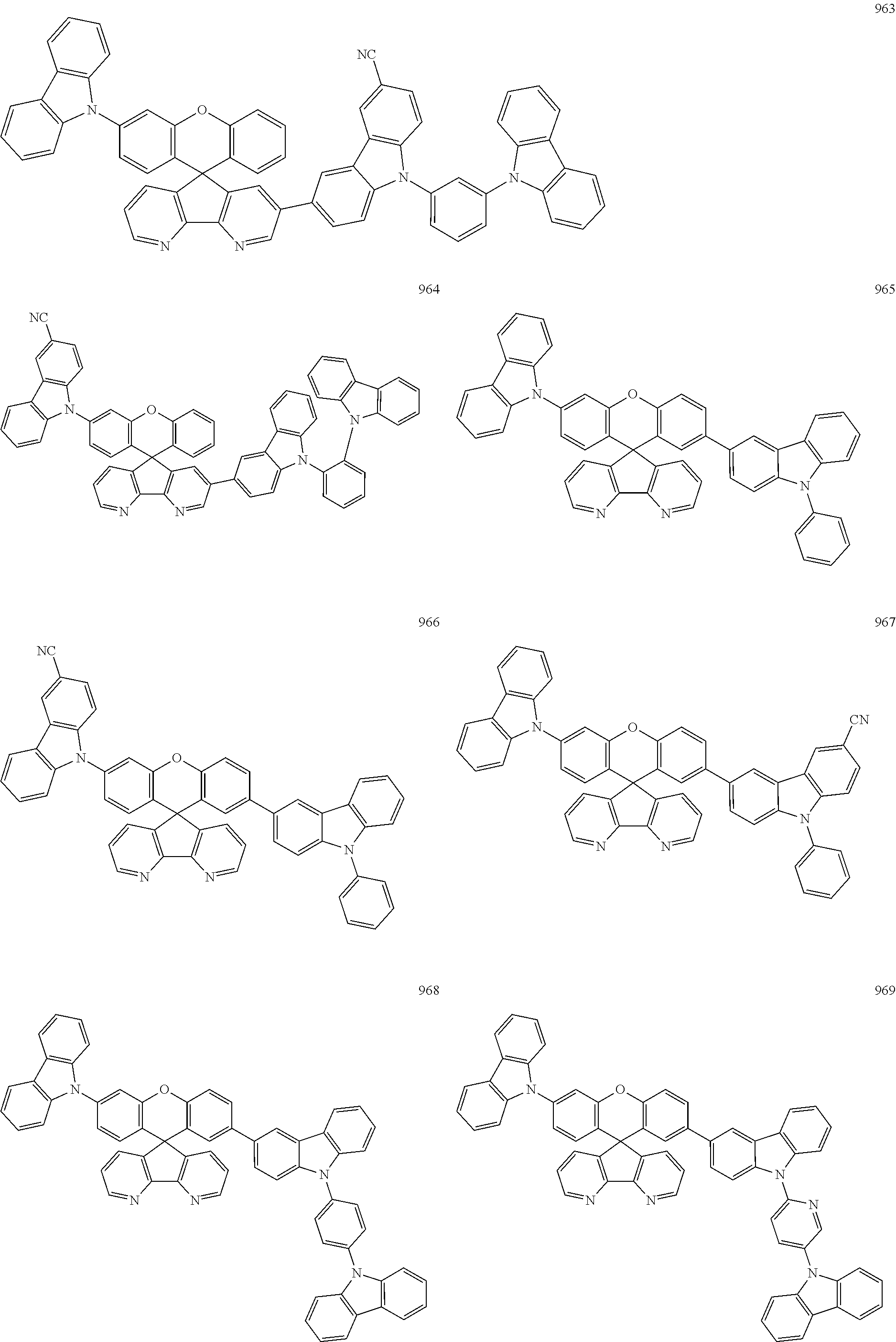
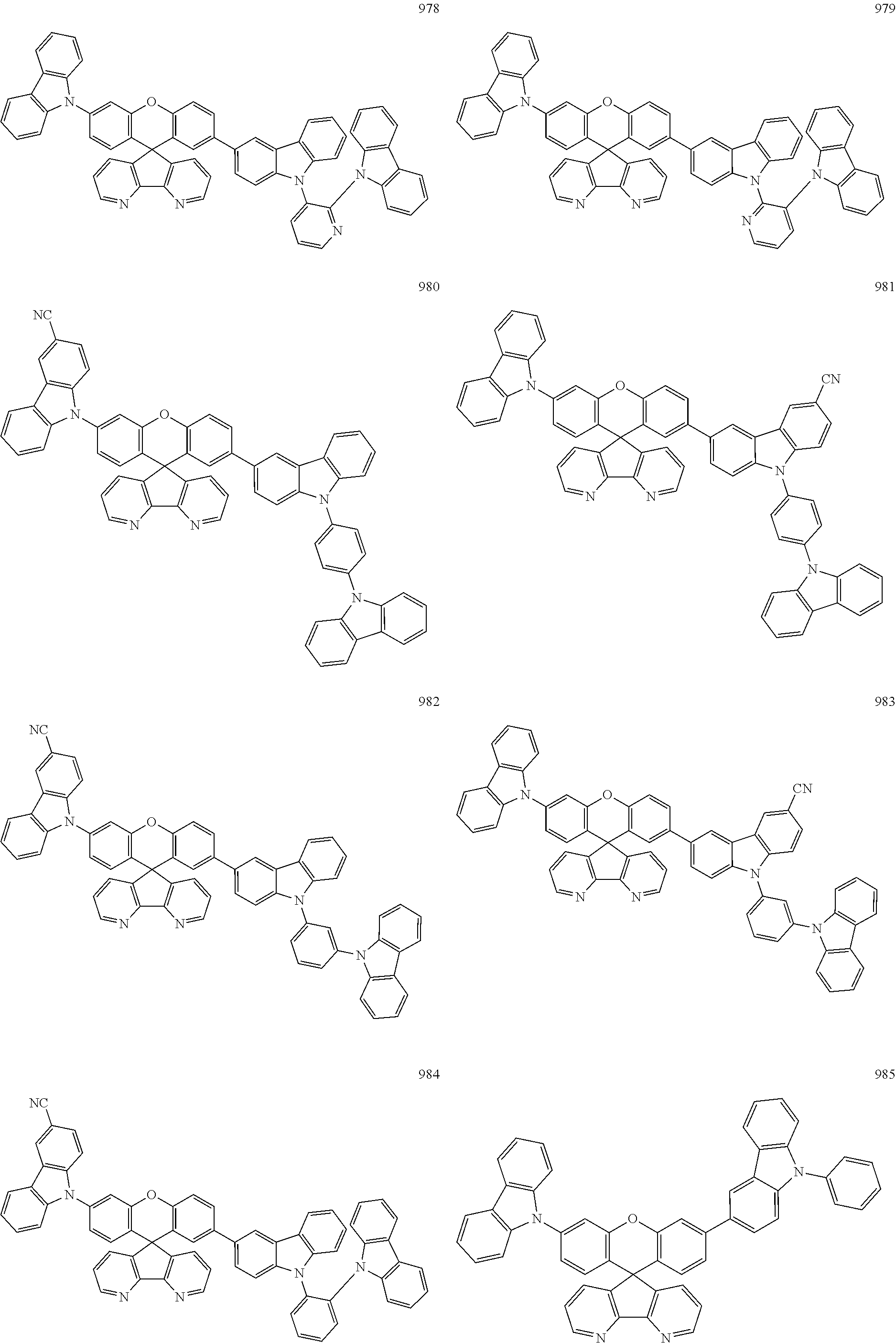
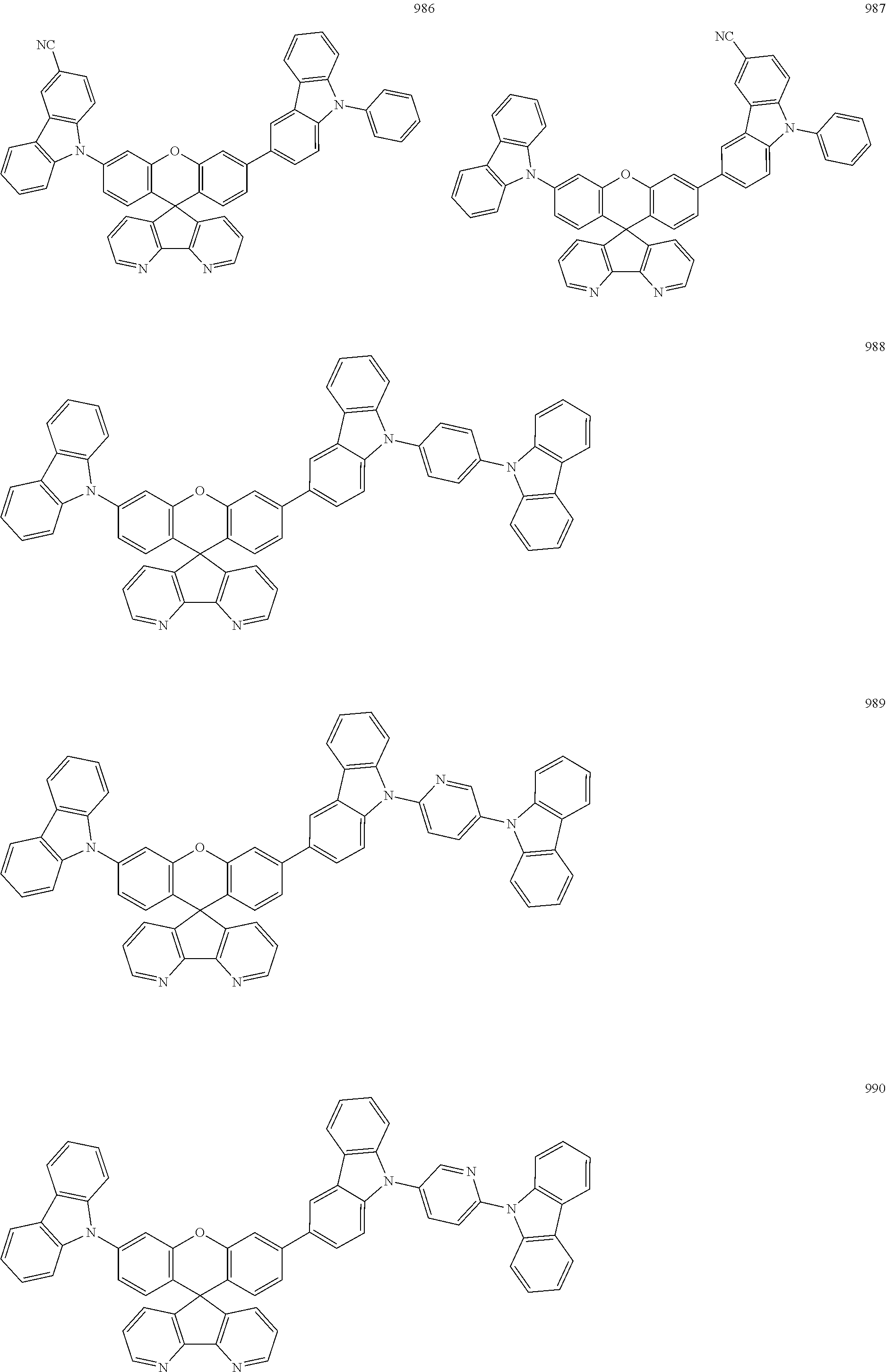
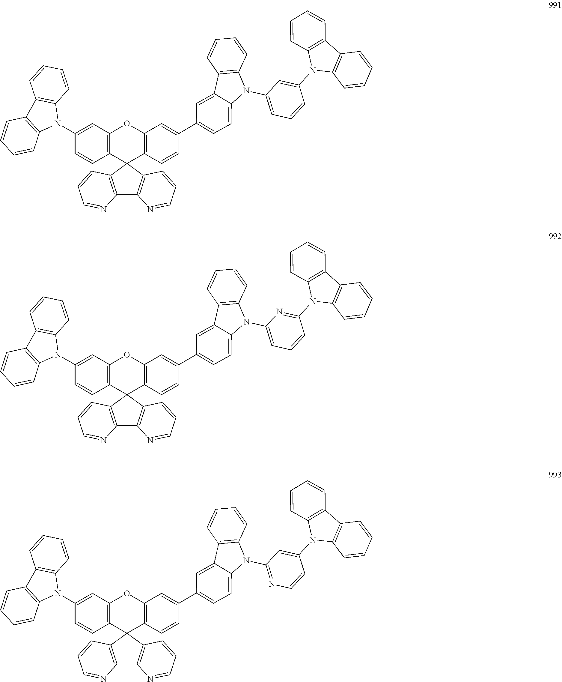
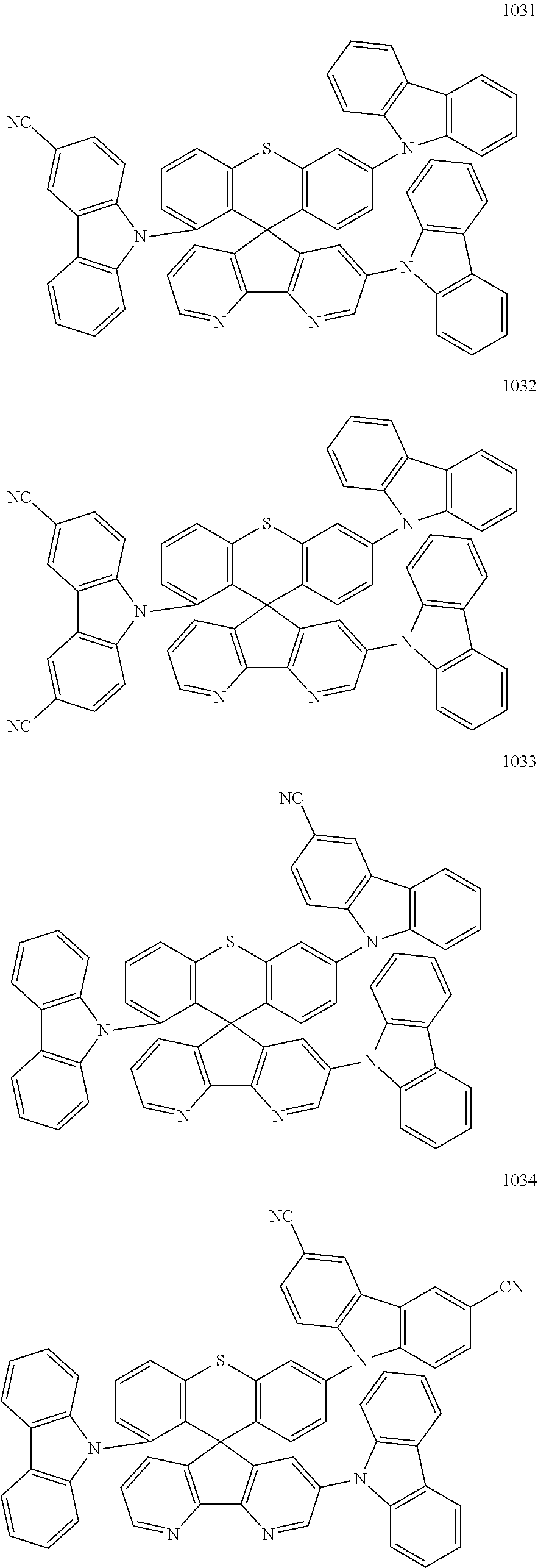
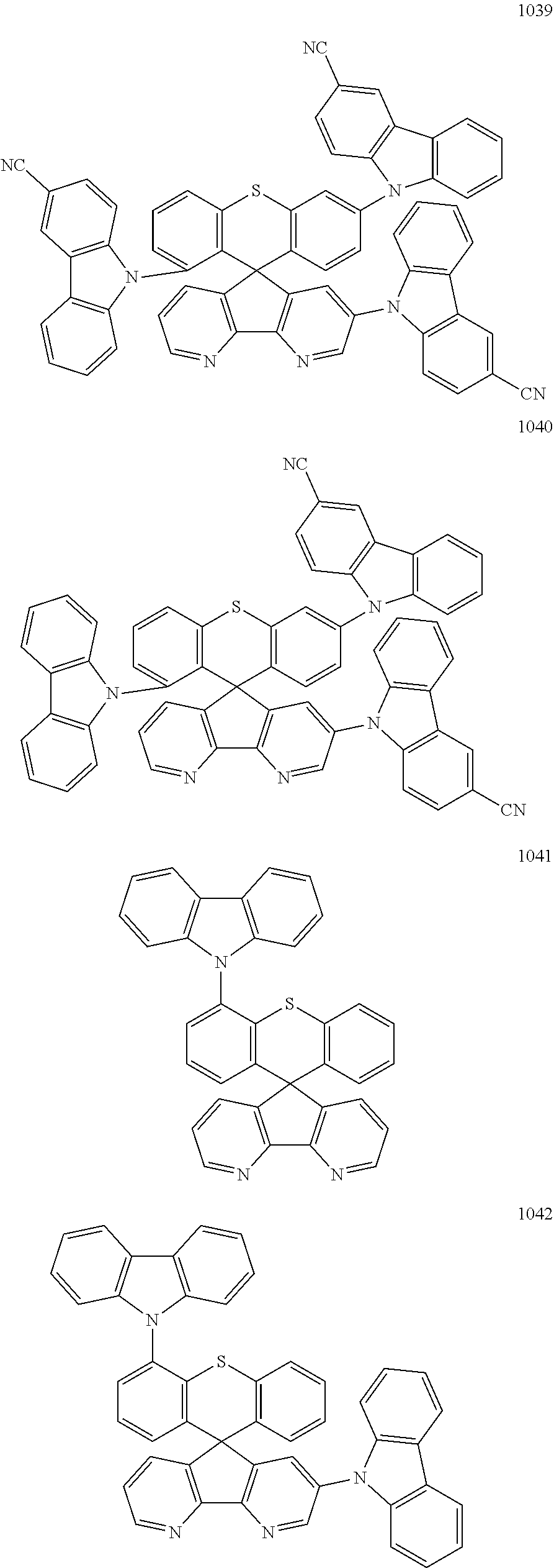
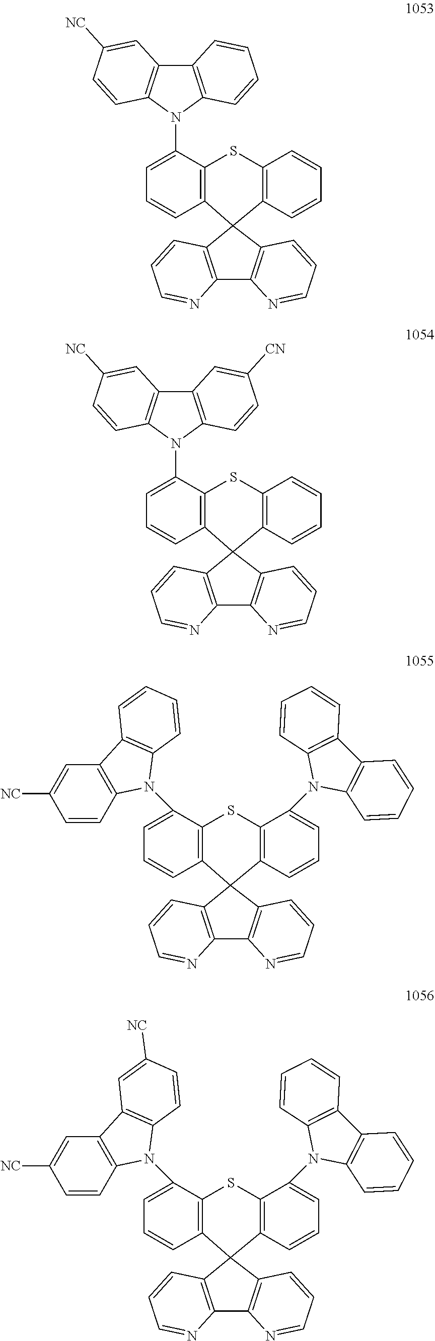
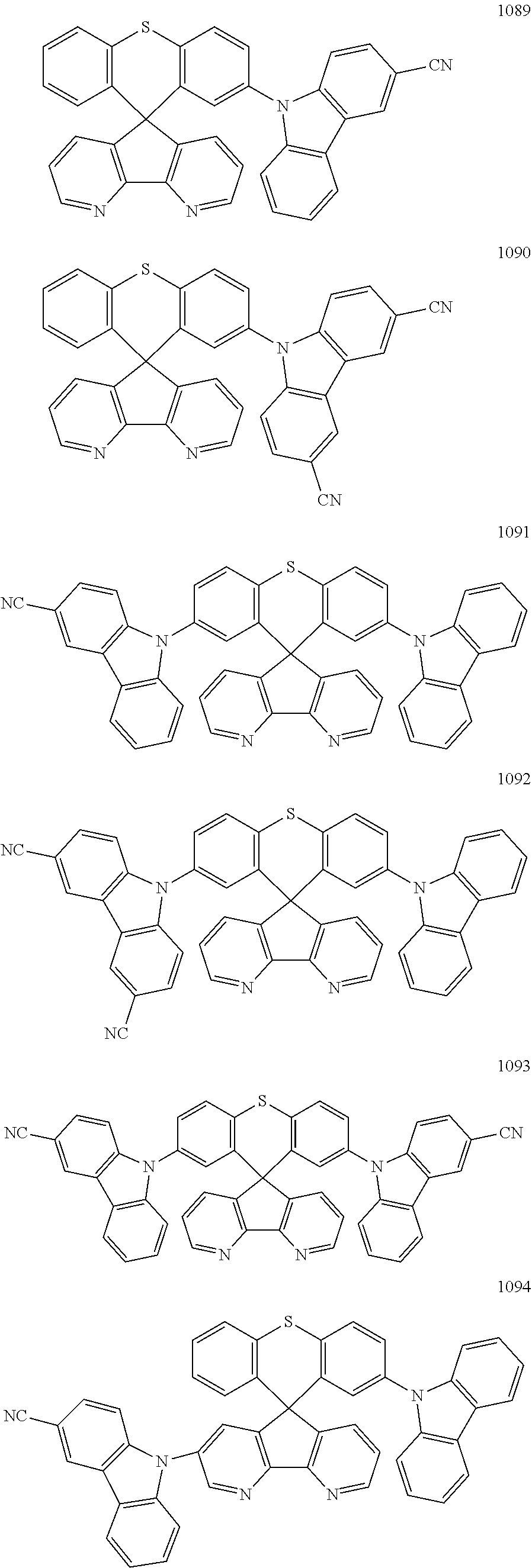
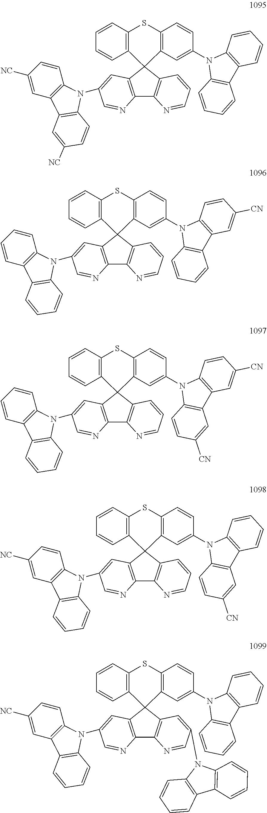
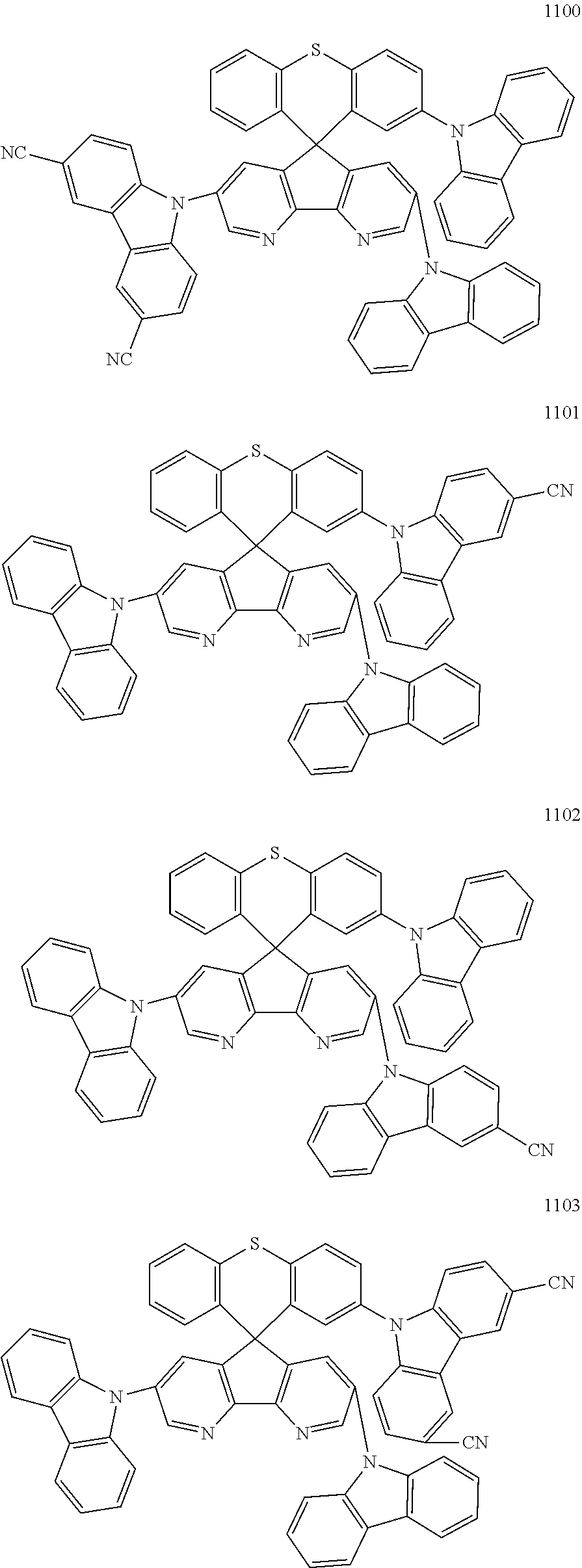
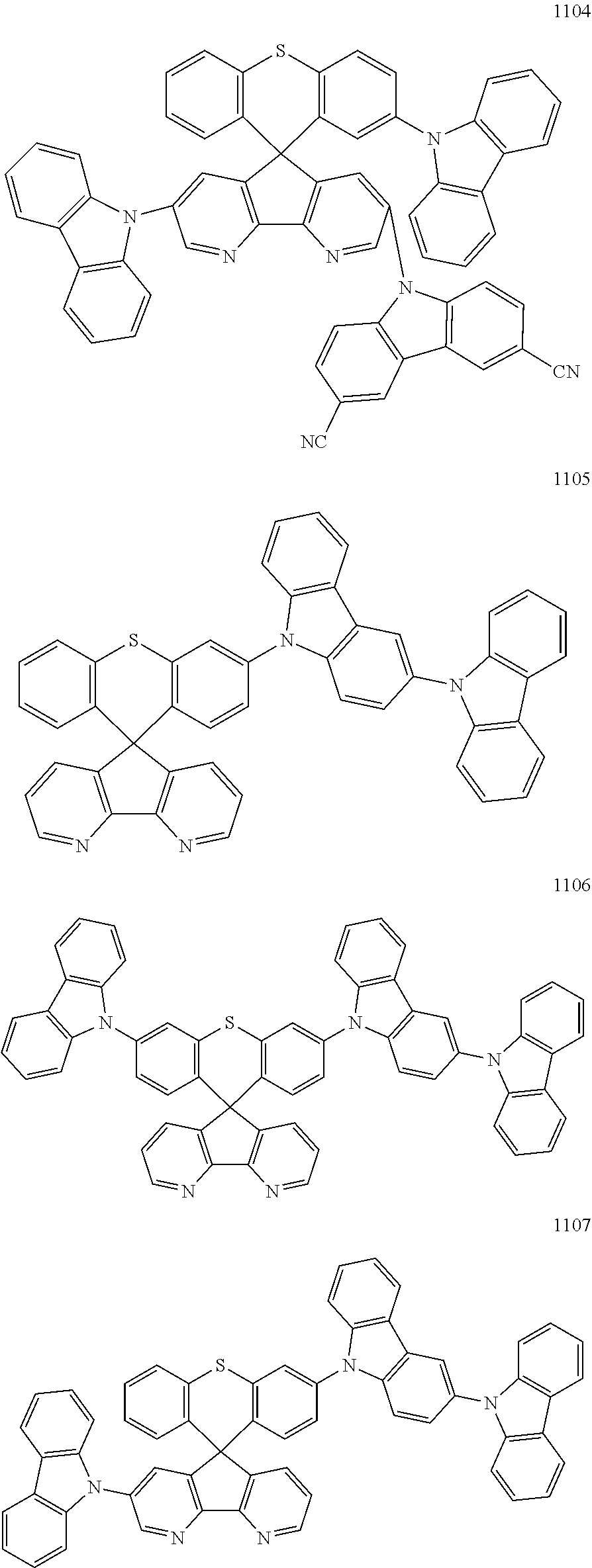
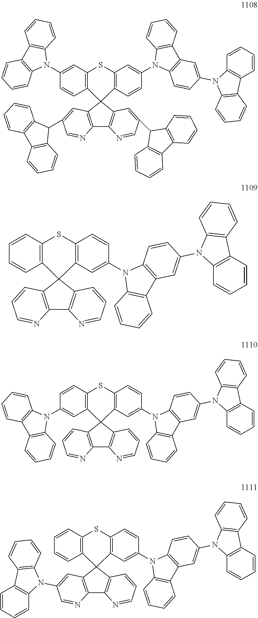
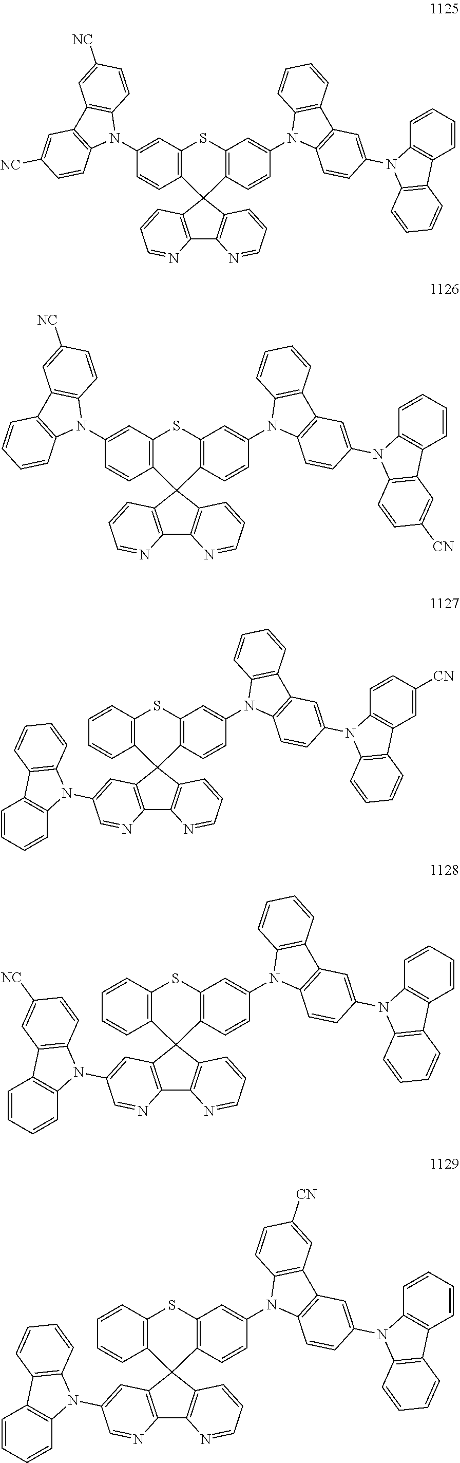
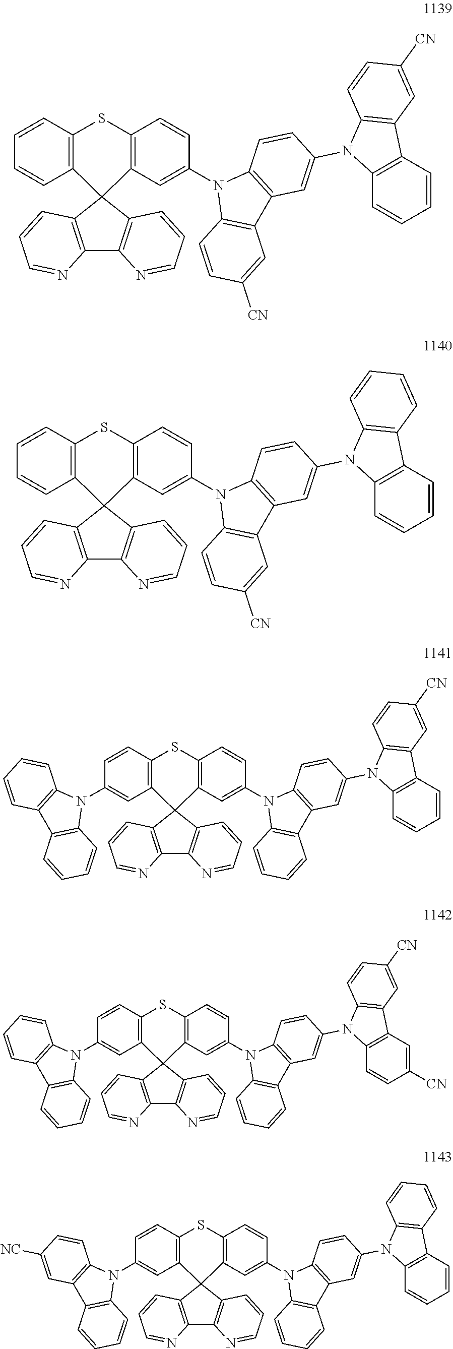
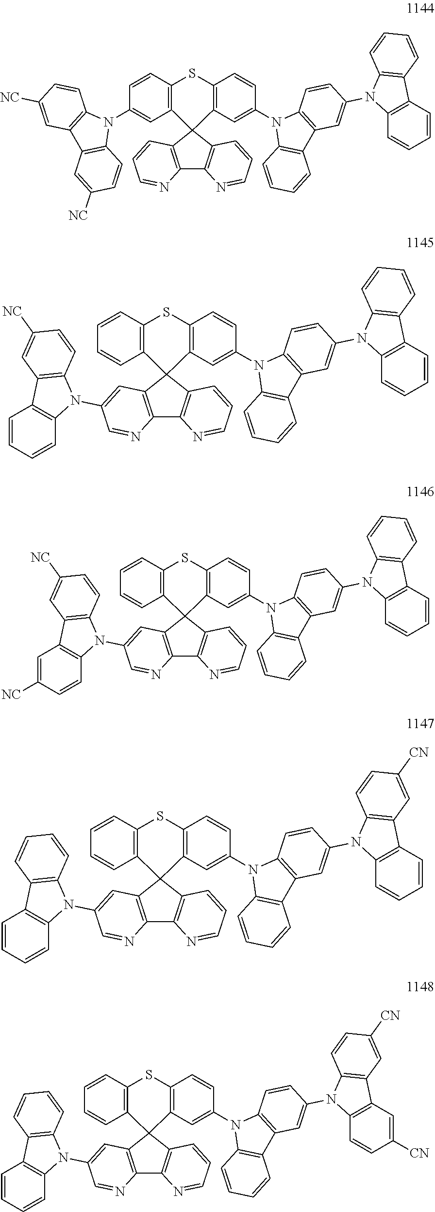
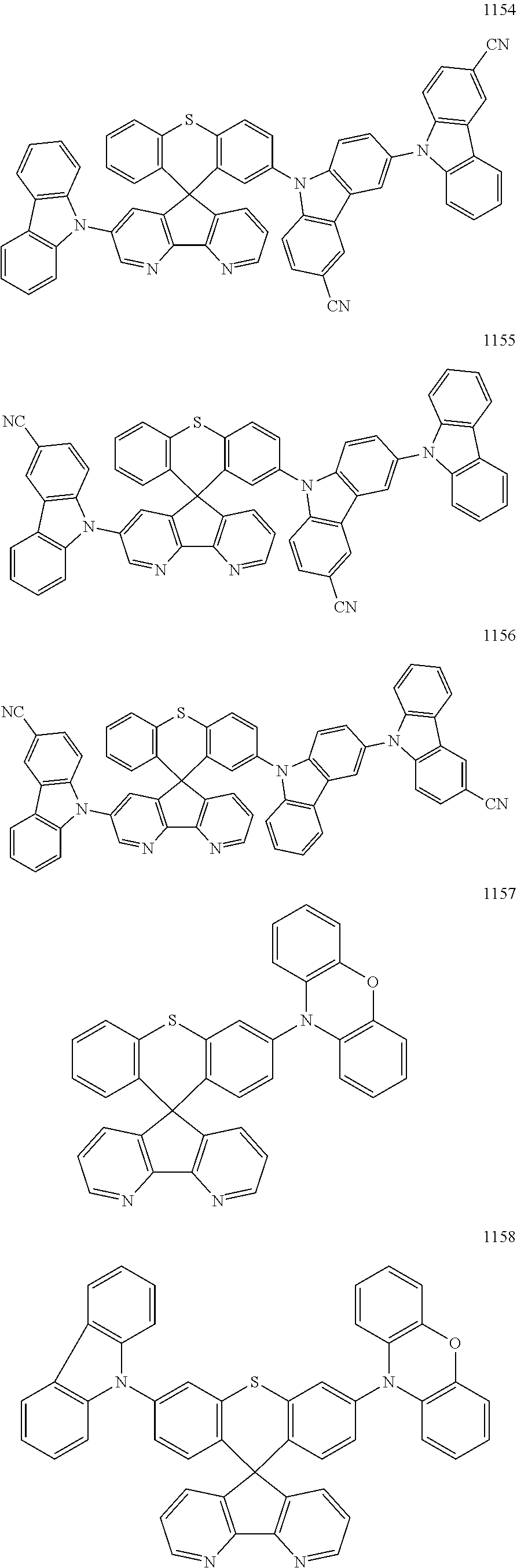
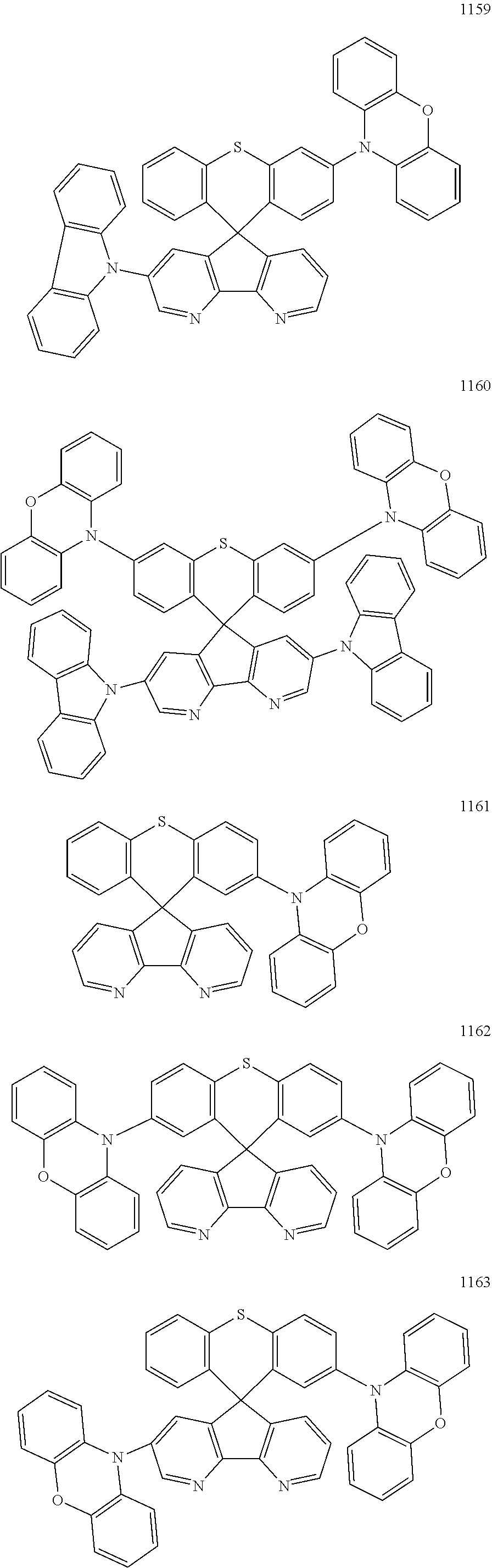
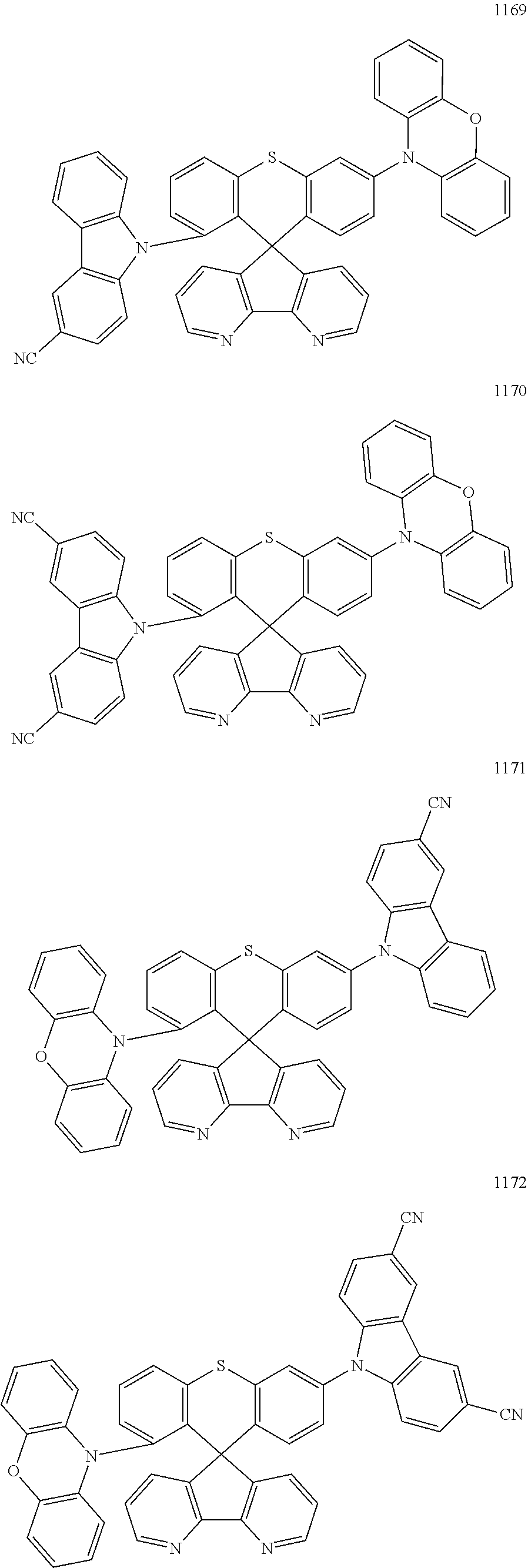
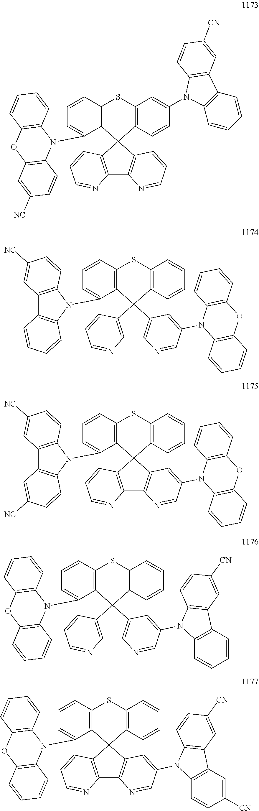
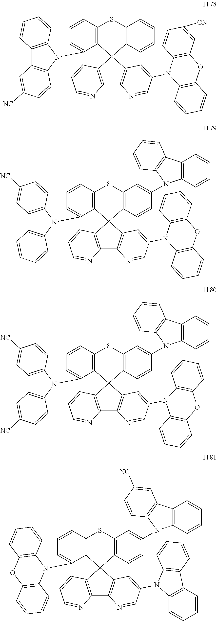
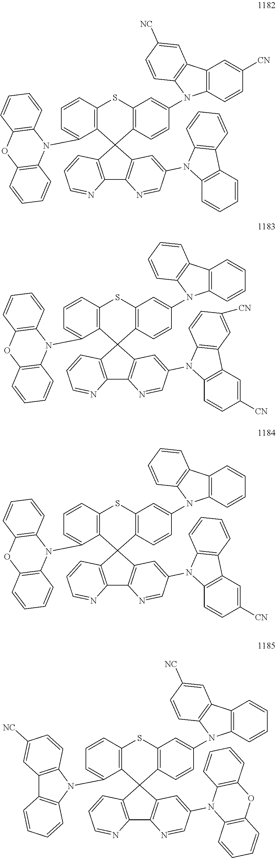
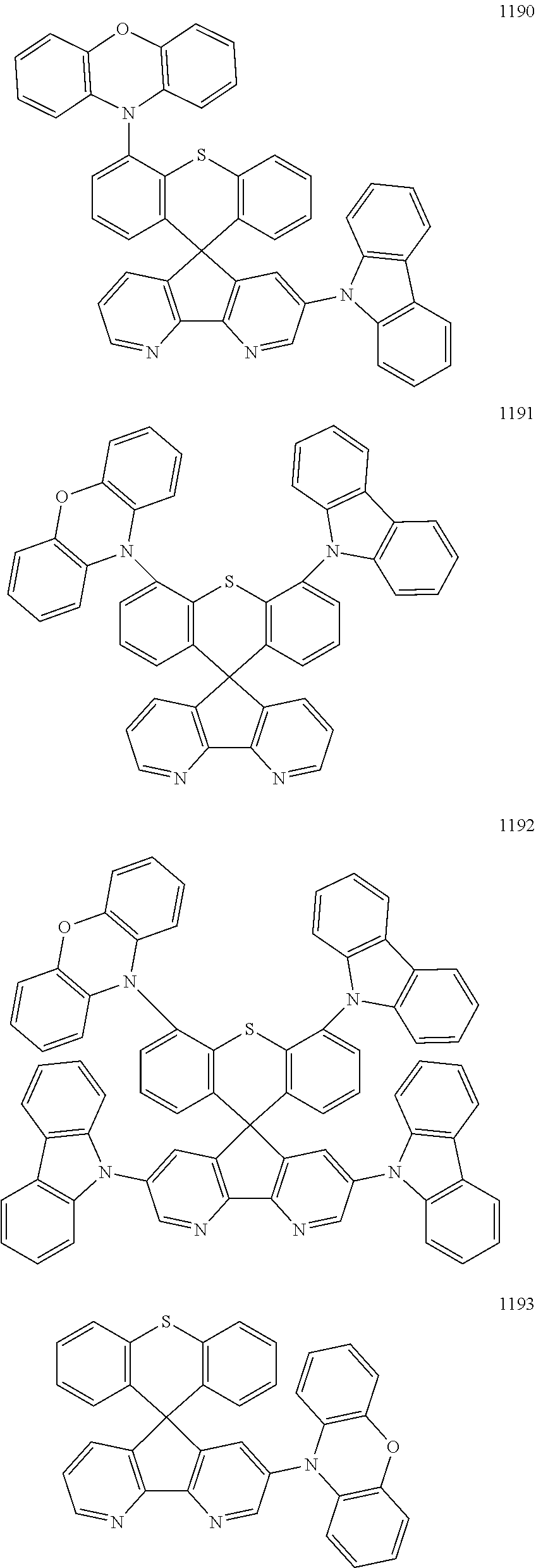
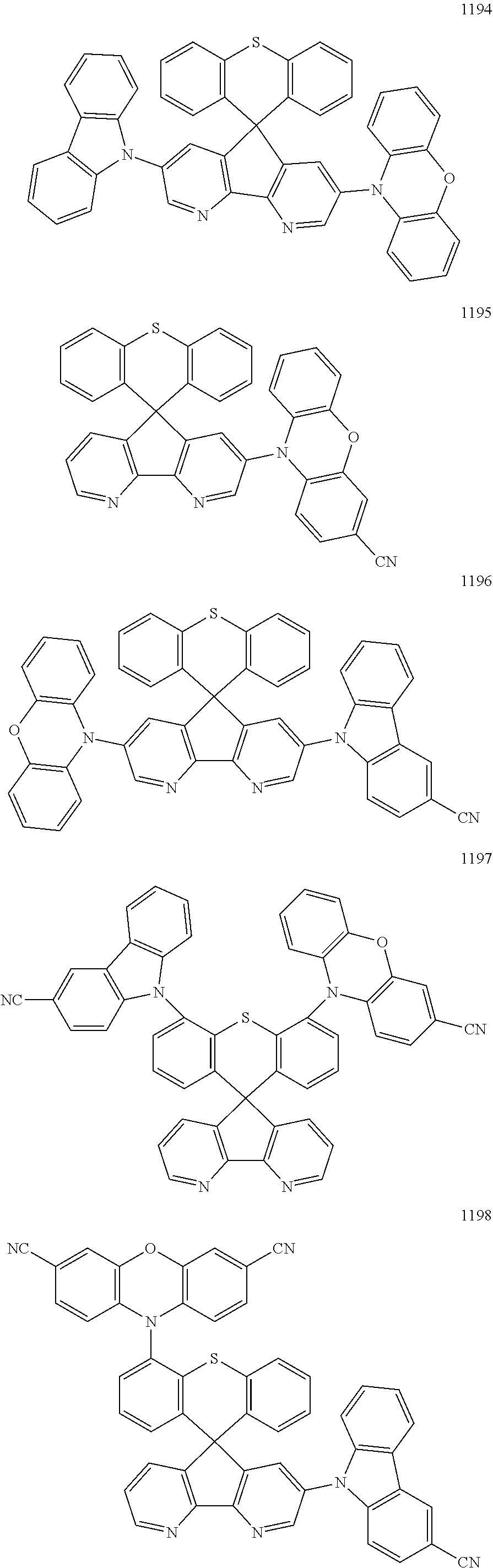
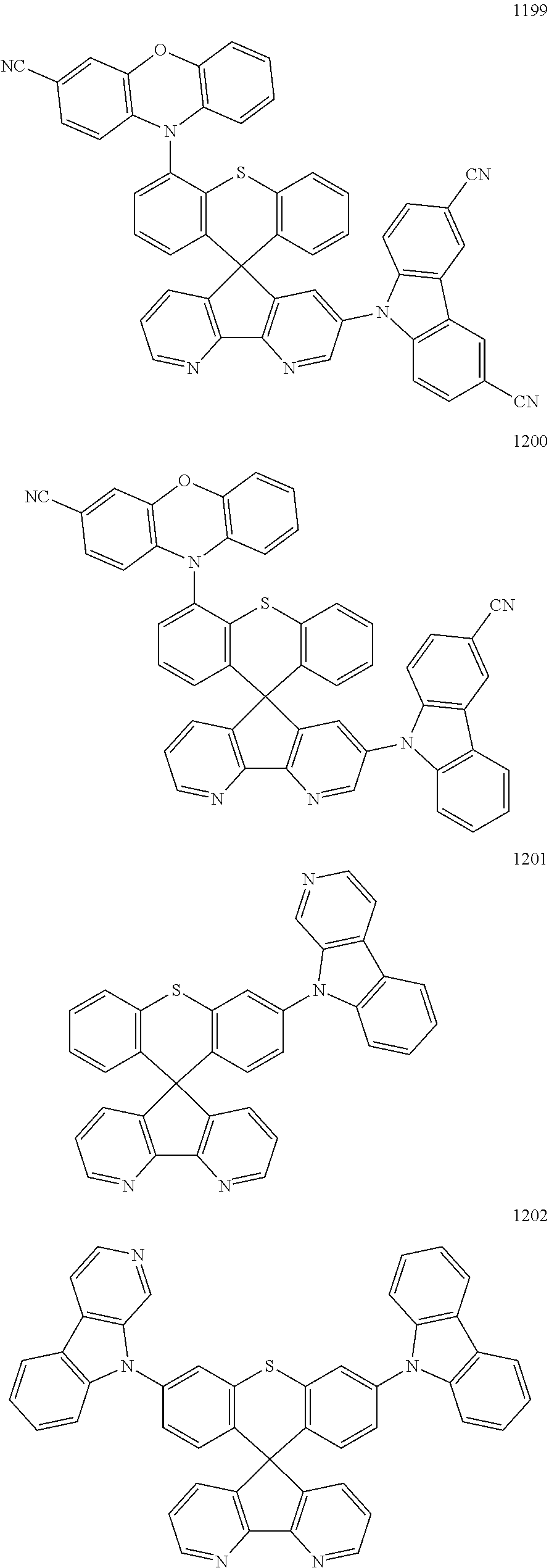
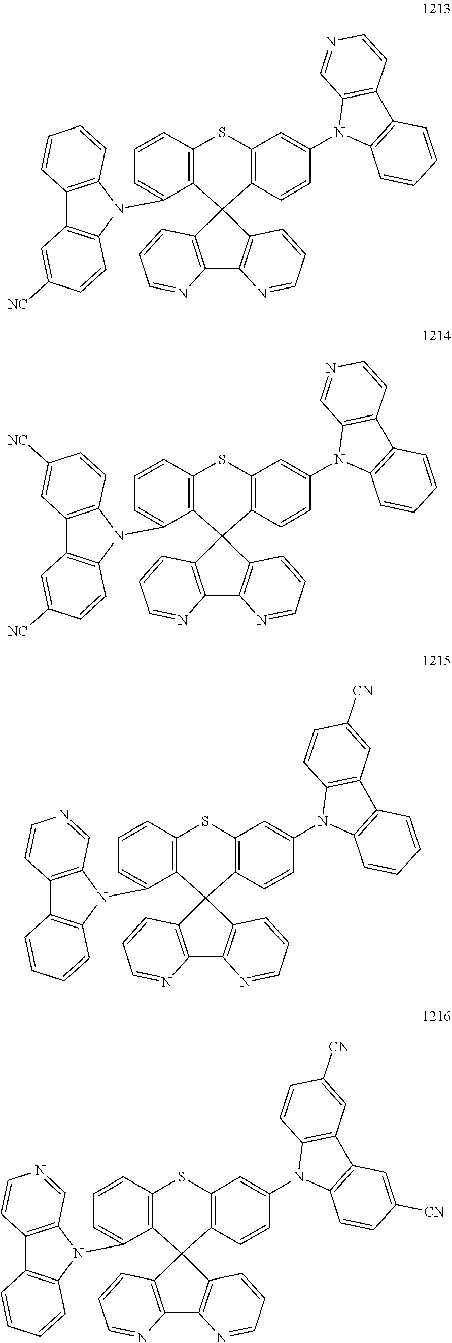
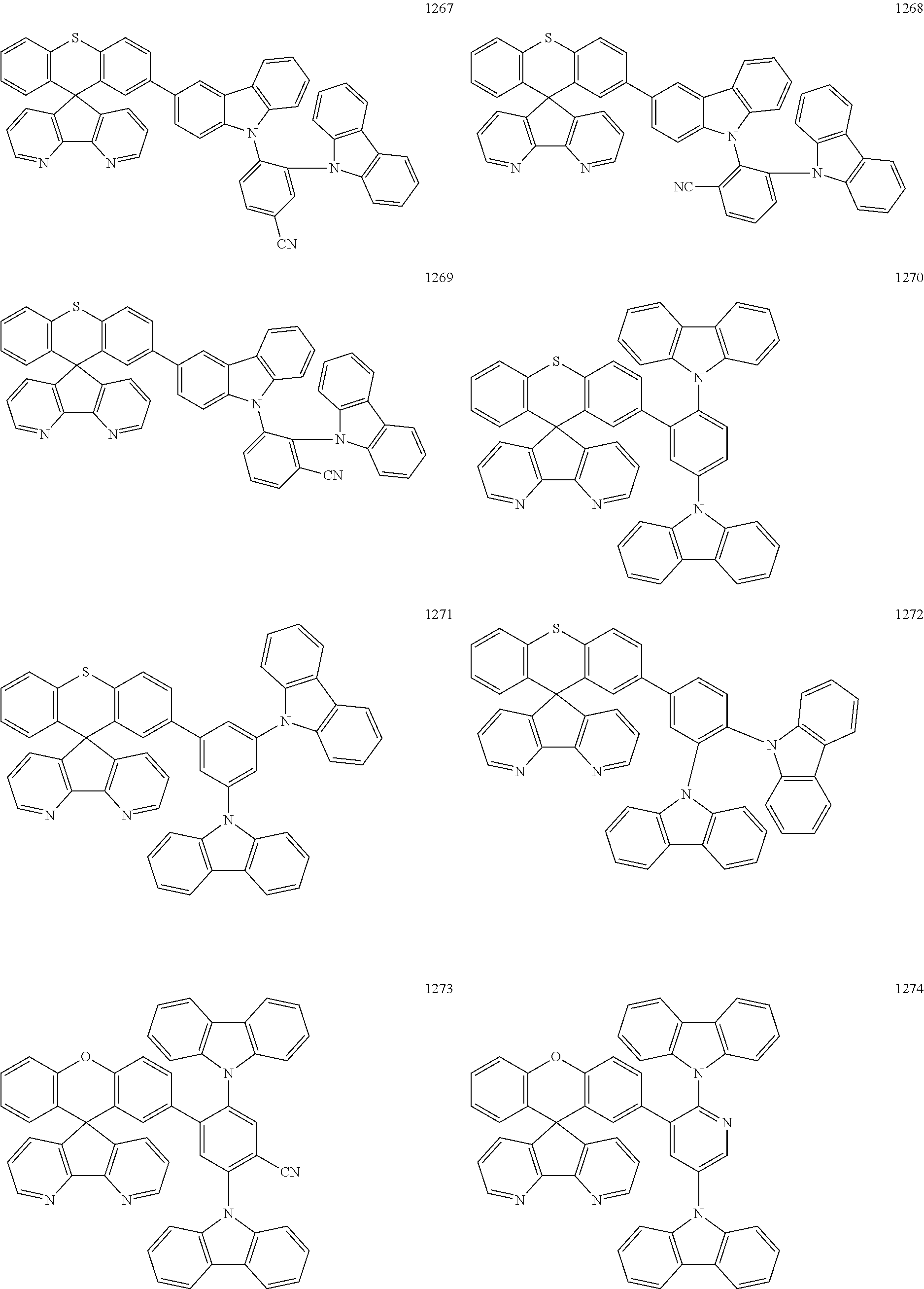
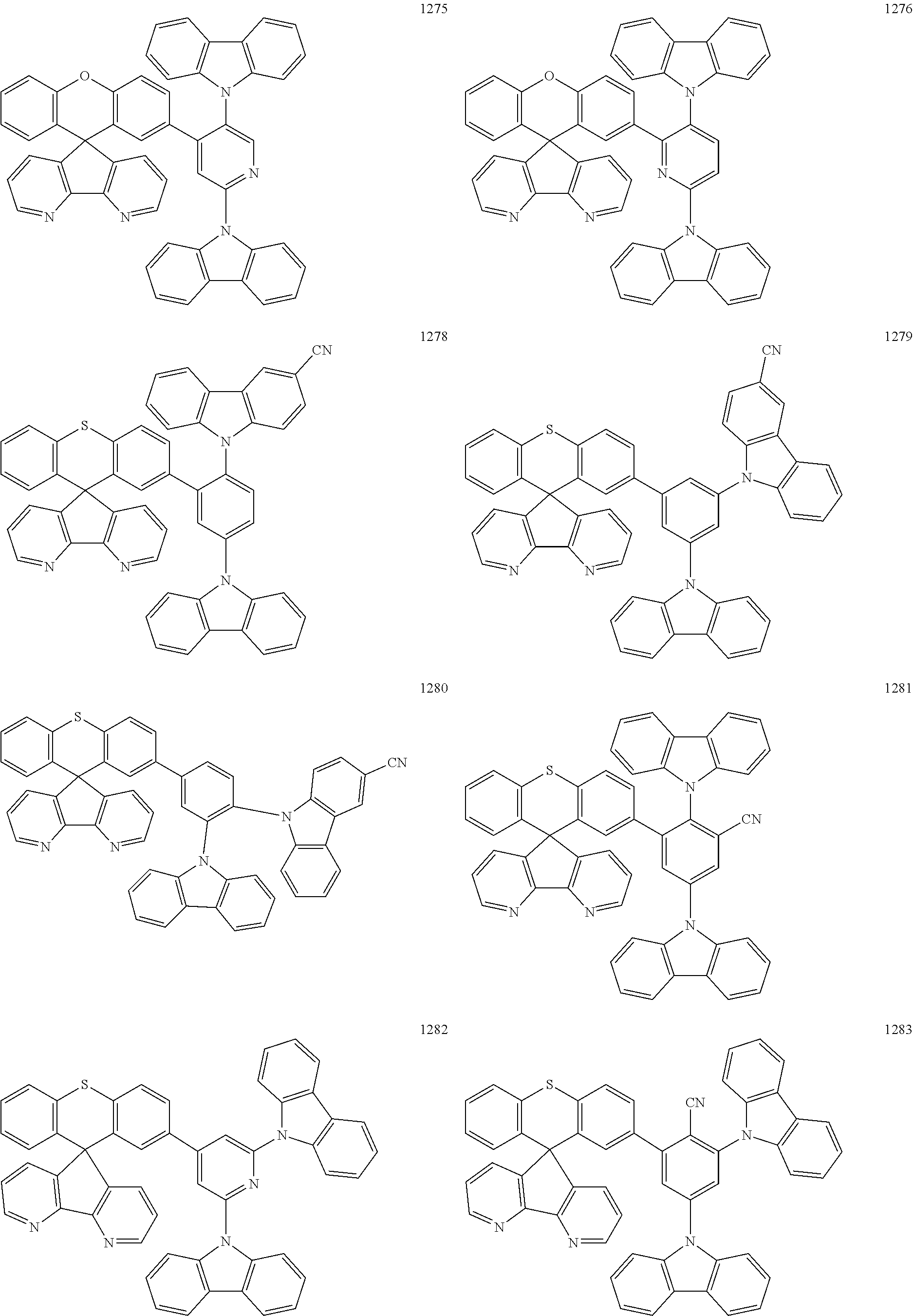
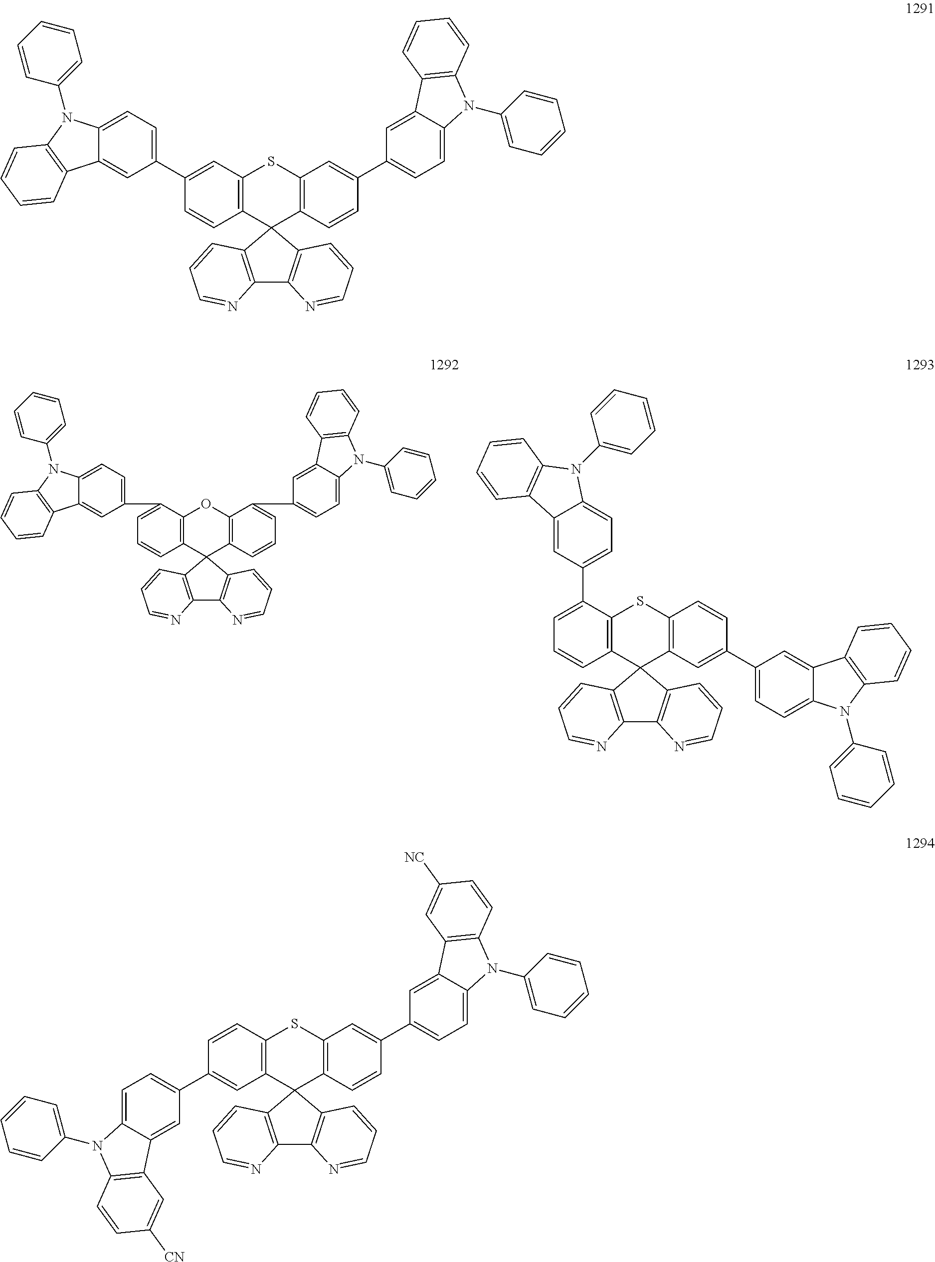
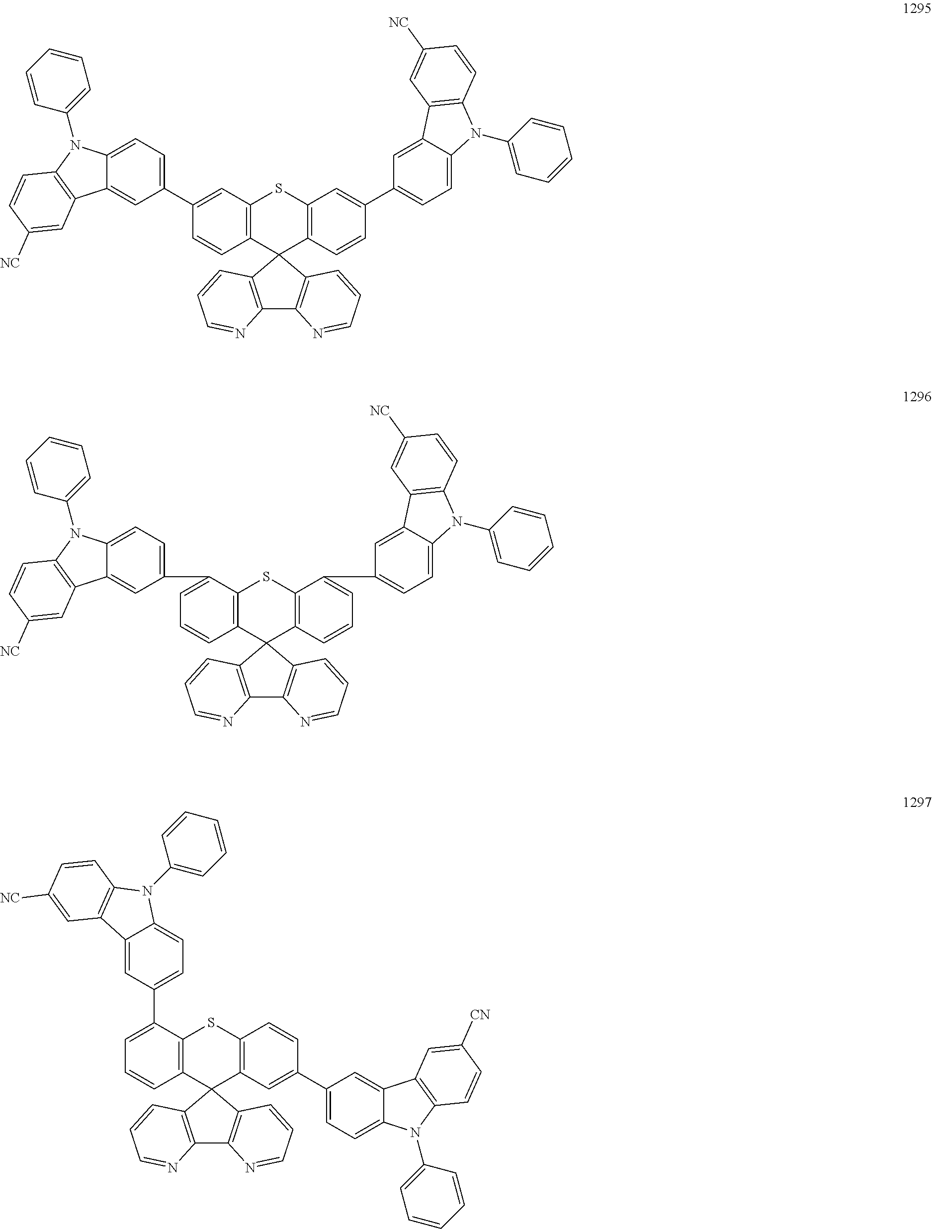
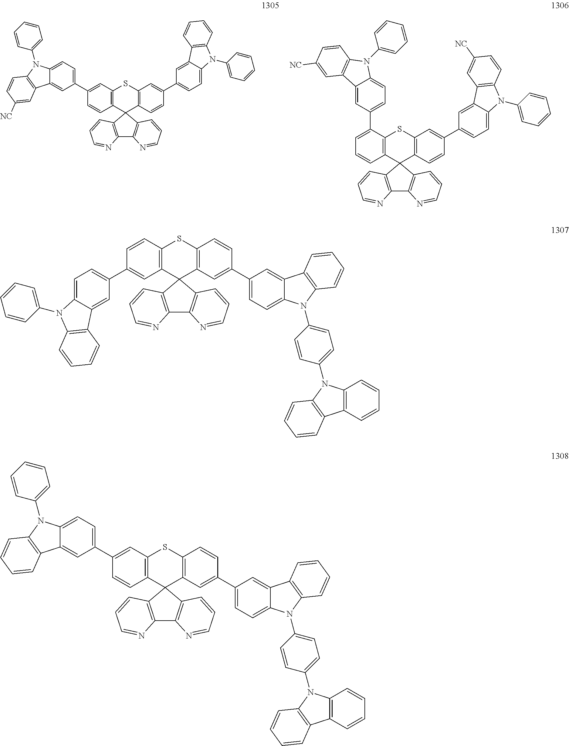
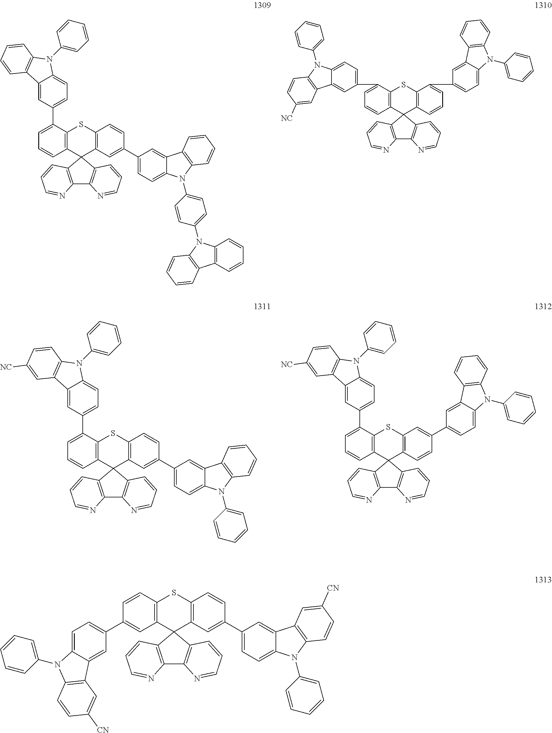
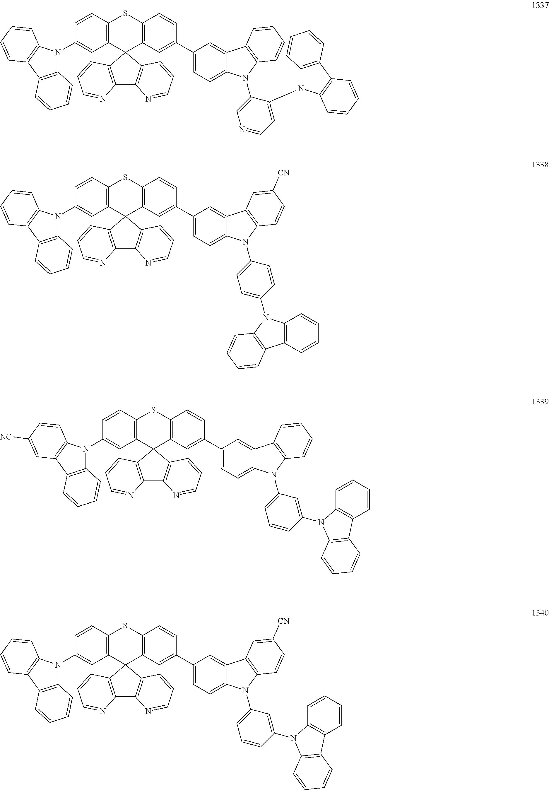
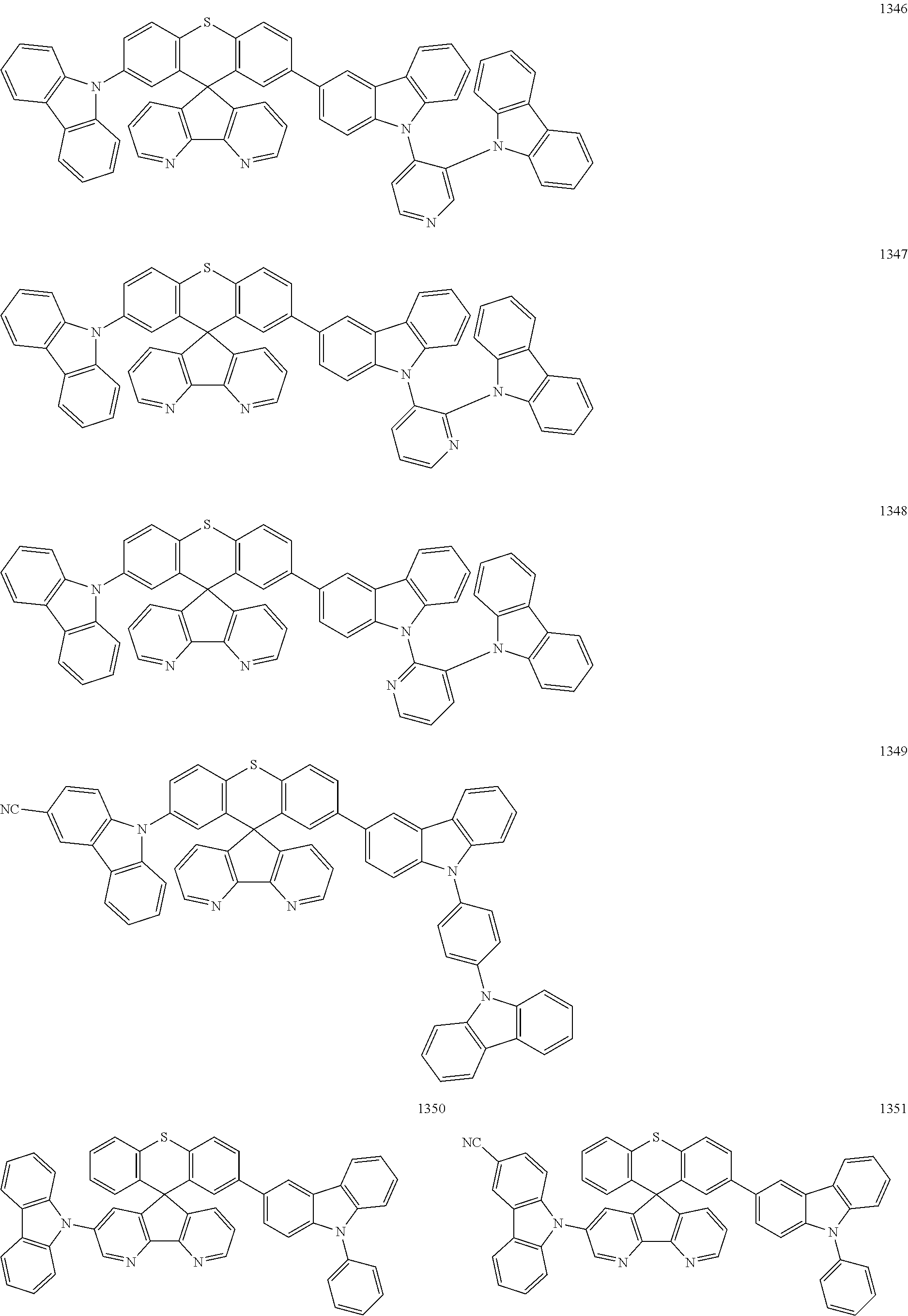
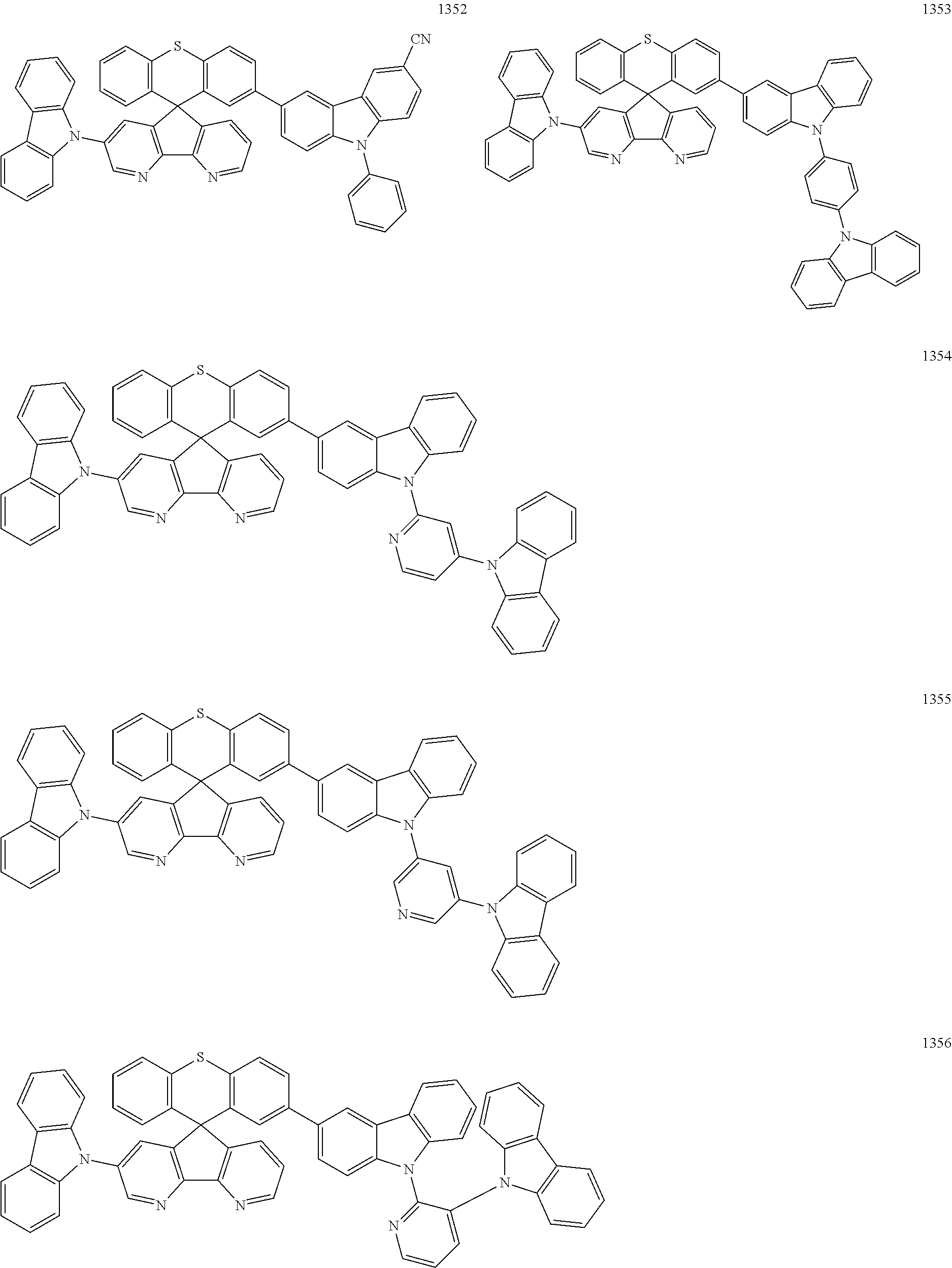
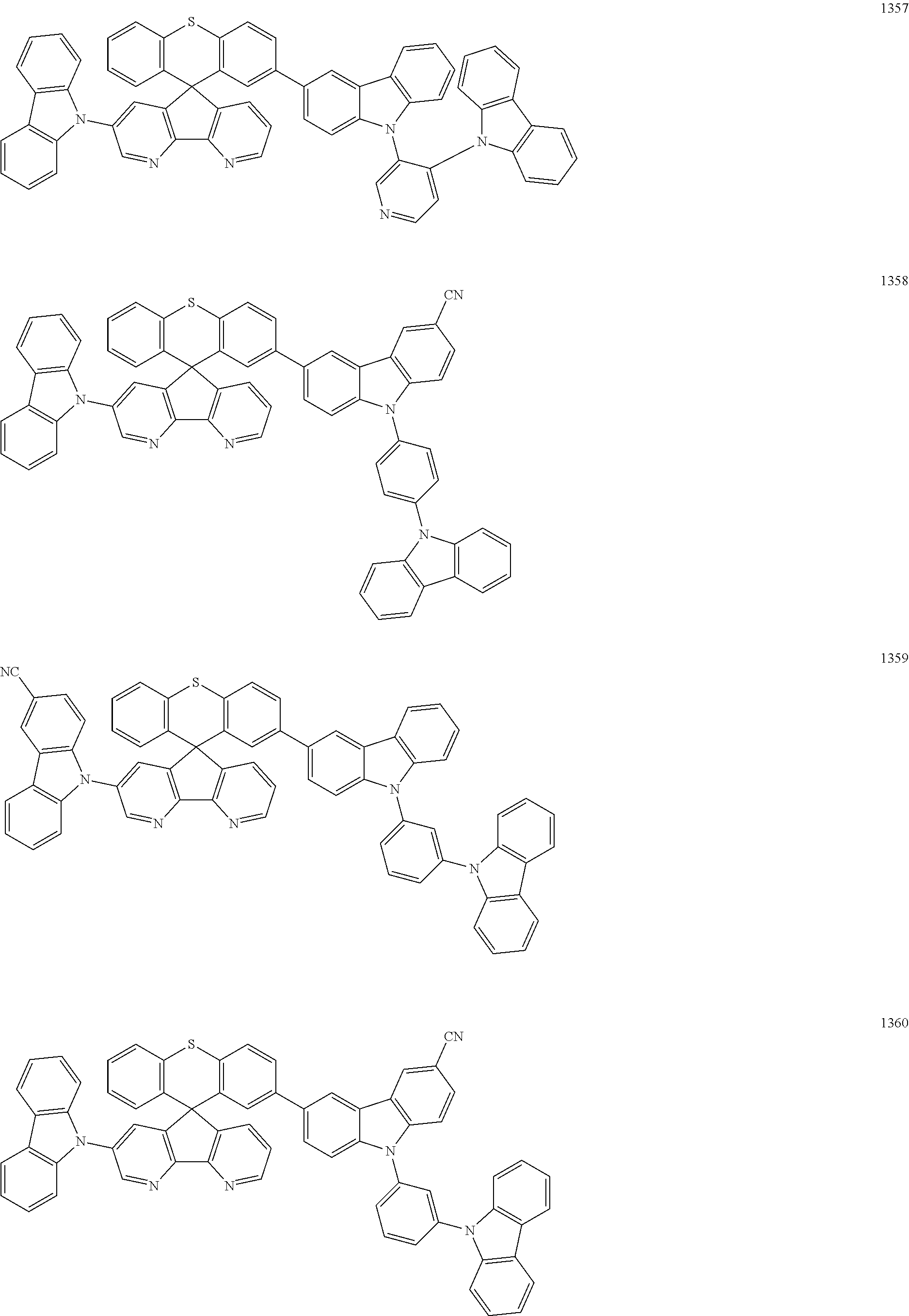
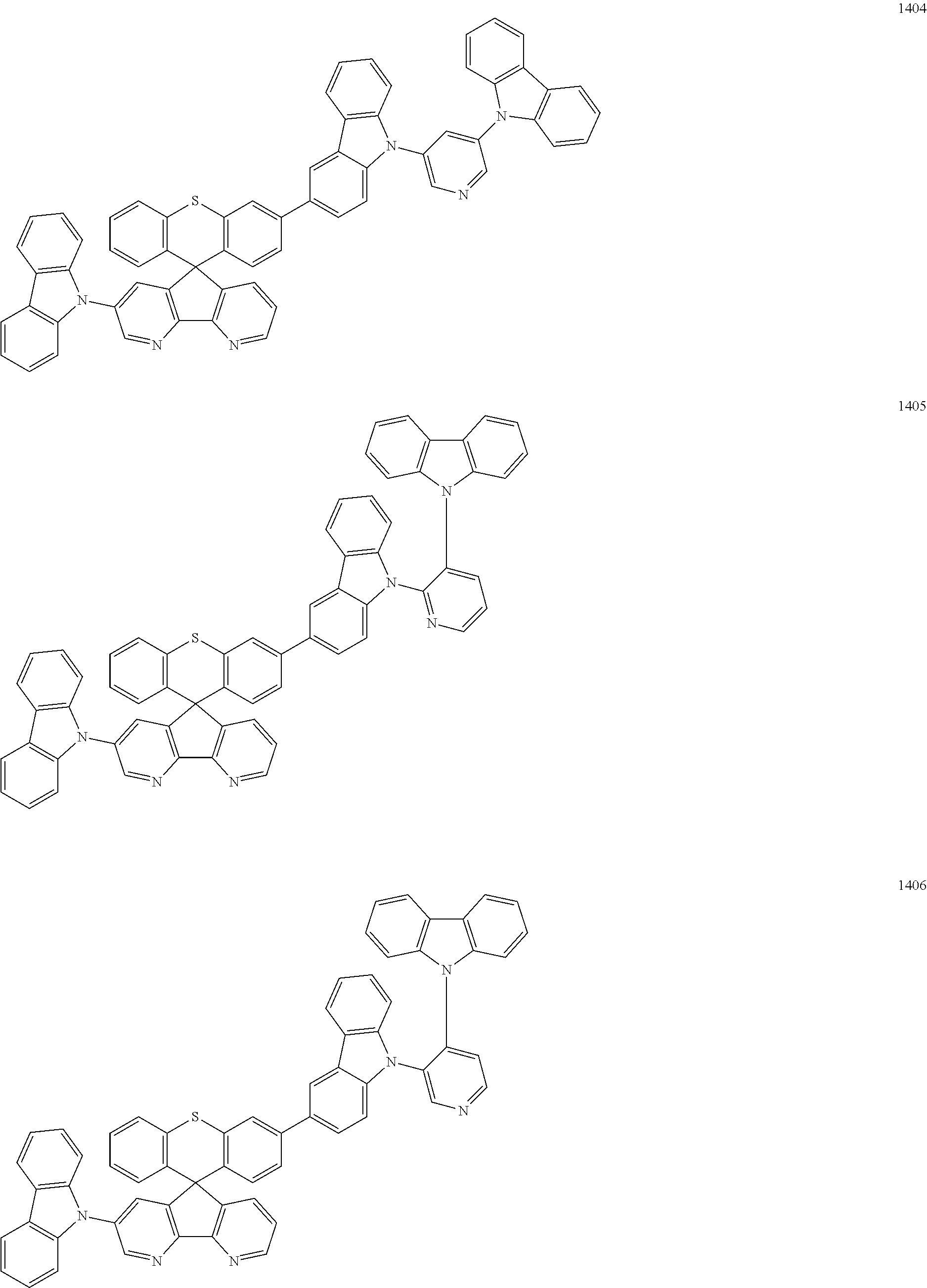
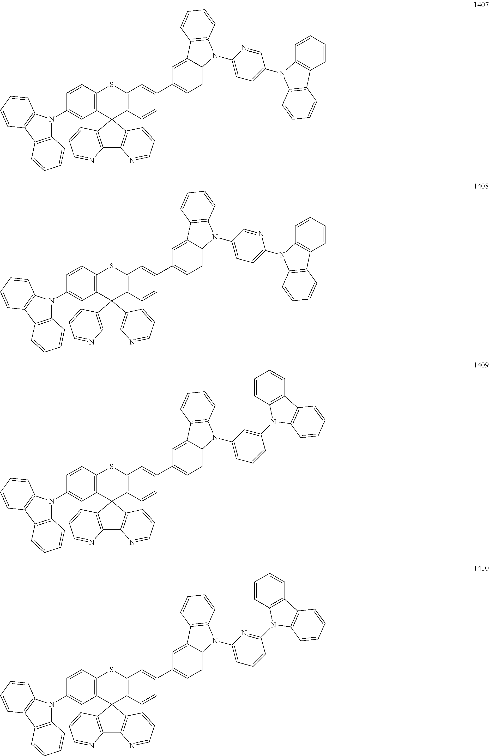
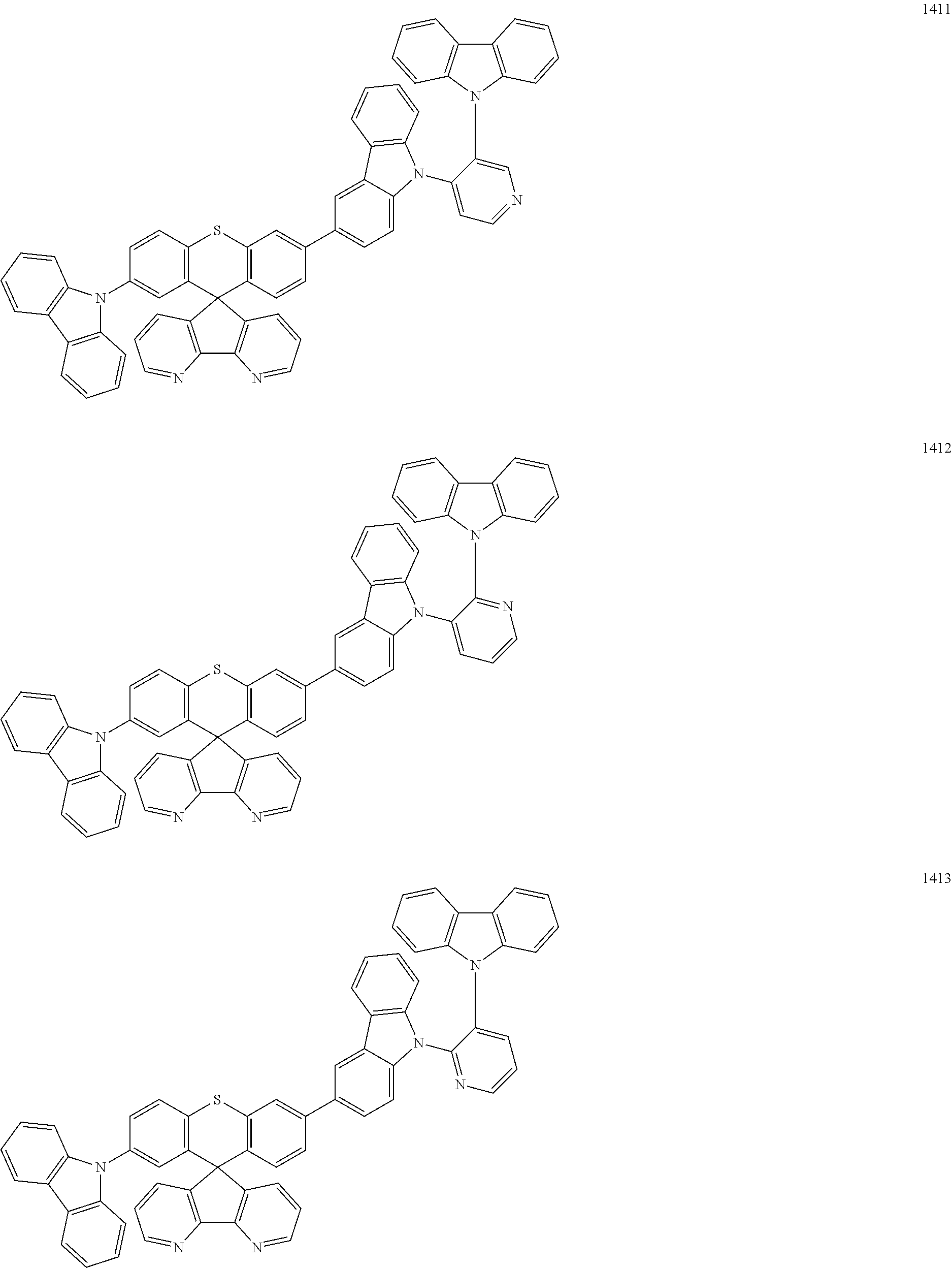
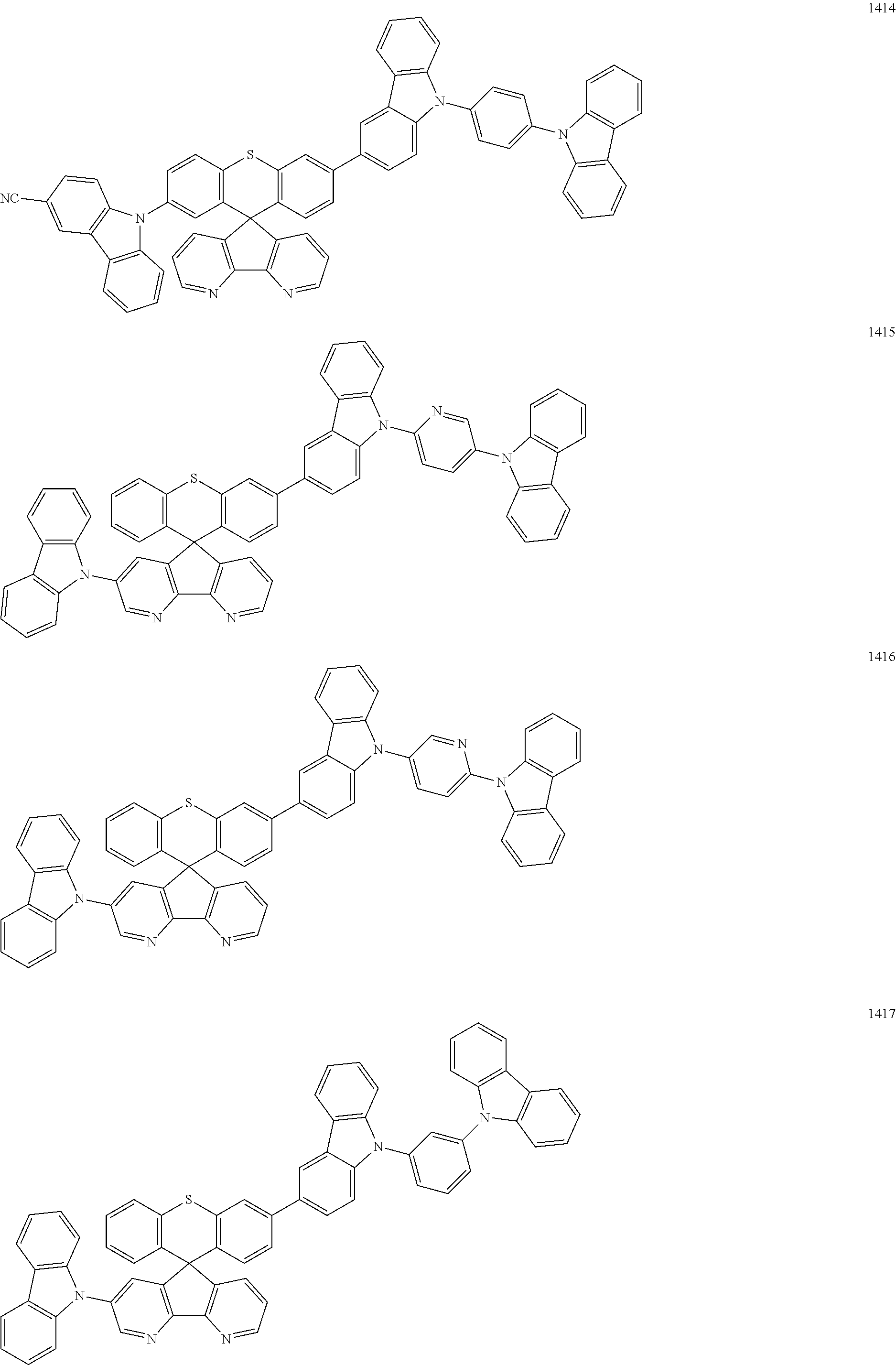
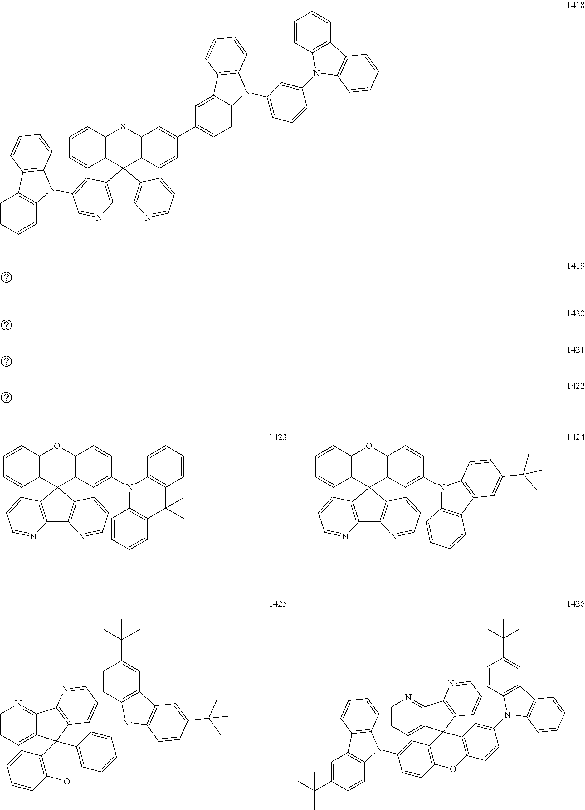
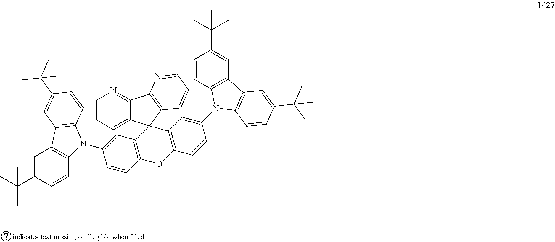
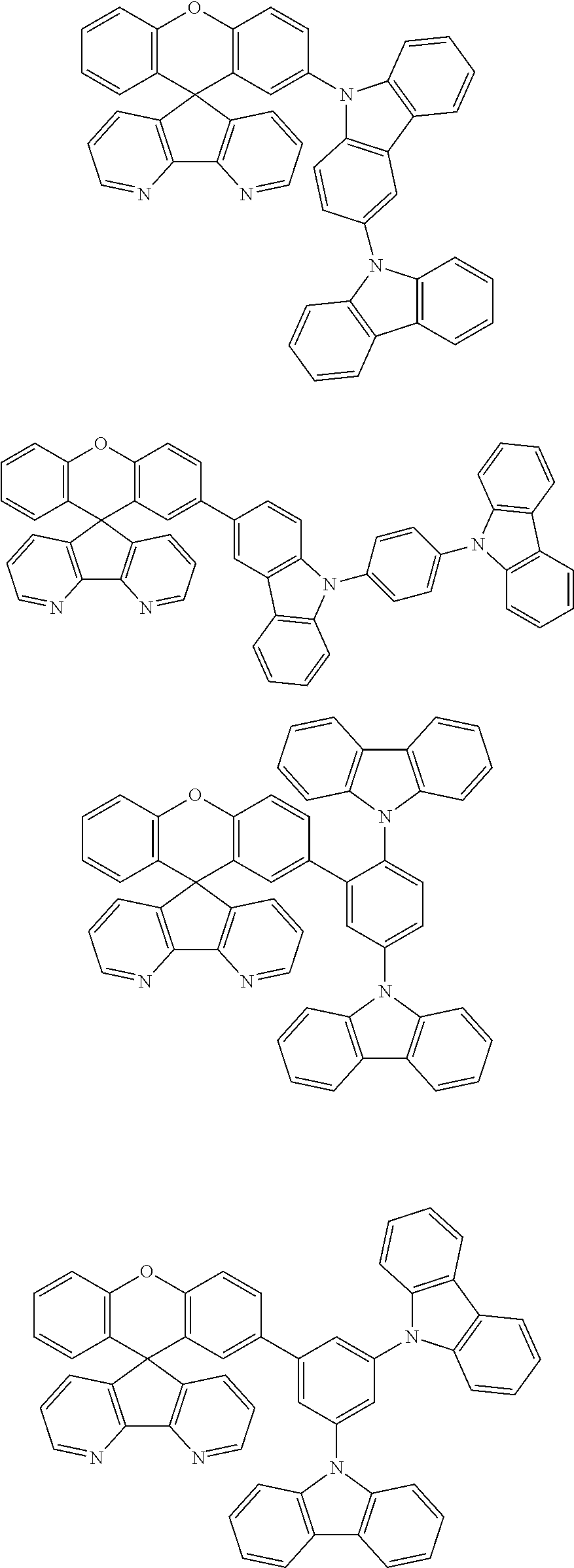
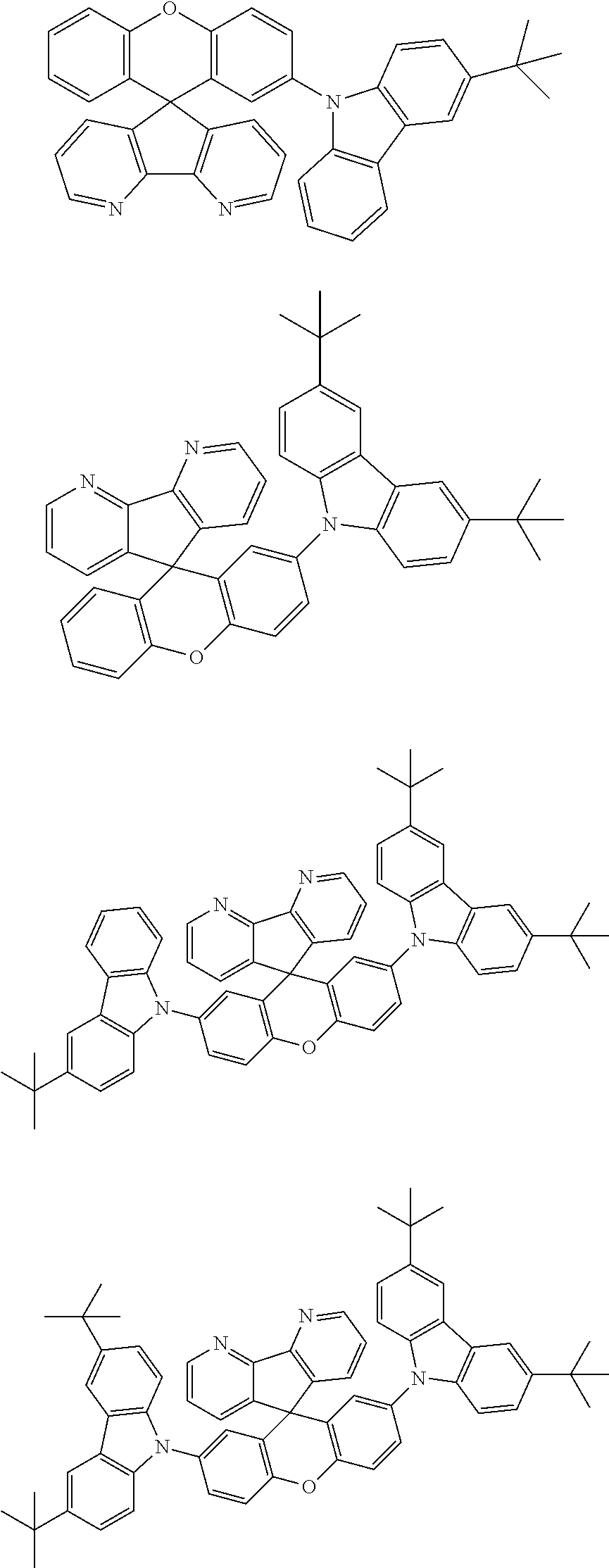
##STR00011## ##STR00012## ##STR00013## ##STR00014## ##STR00015## ##STR00016## ##STR00017## ##STR00018## ##STR00019## ##STR00020## ##STR00021## ##STR00022## ##STR00023## ##STR00024## ##STR00025## ##STR00026## ##STR00027## ##STR00028## ##STR00029## ##STR00030## ##STR00031## ##STR00032## ##STR00033## ##STR00034## ##STR00035## ##STR00036## ##STR00037## ##STR00038## ##STR00039## ##STR00040## ##STR00041## ##STR00042## ##STR00043## ##STR00044## ##STR00045## ##STR00046## ##STR00047## ##STR00048## ##STR00049## ##STR00050## ##STR00051## ##STR00052## ##STR00053## ##STR00054## ##STR00055## ##STR00056## ##STR00057## ##STR00058## ##STR00059## ##STR00060## ##STR00061## ##STR00062## ##STR00063## ##STR00064## ##STR00065## ##STR00066## ##STR00067## ##STR00068##
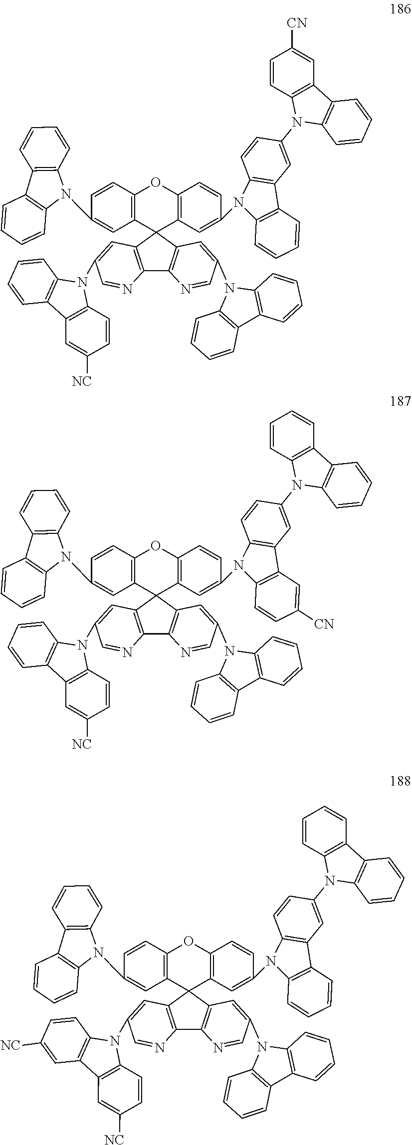
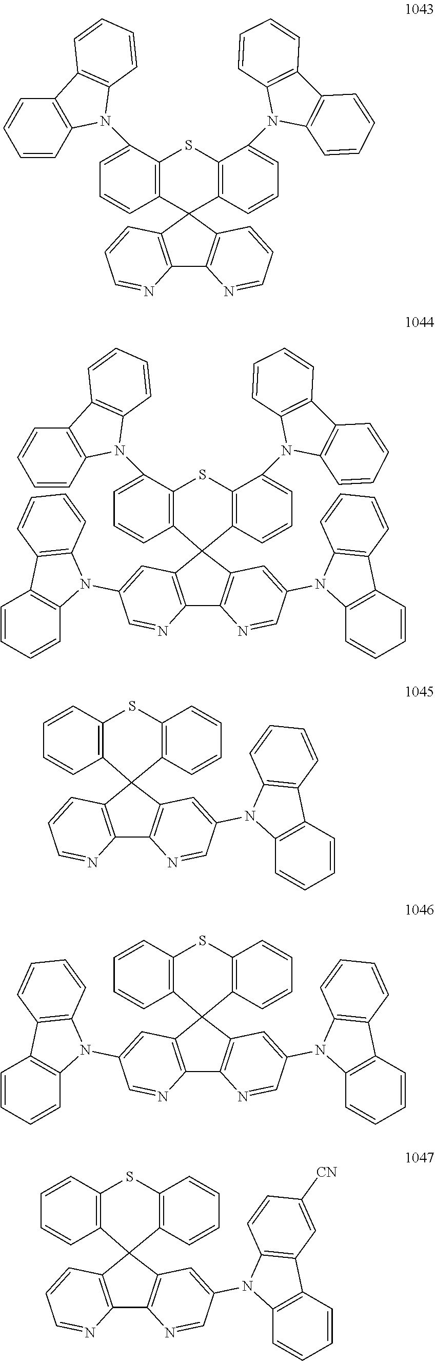
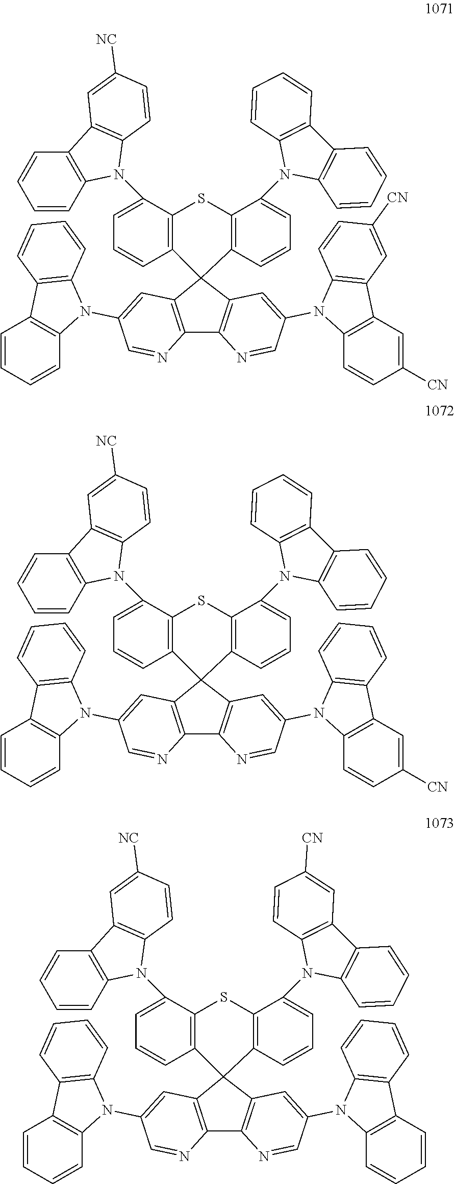
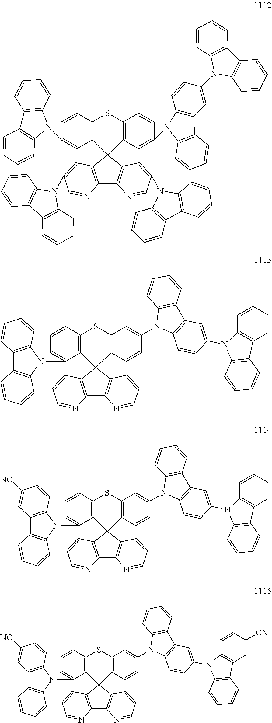
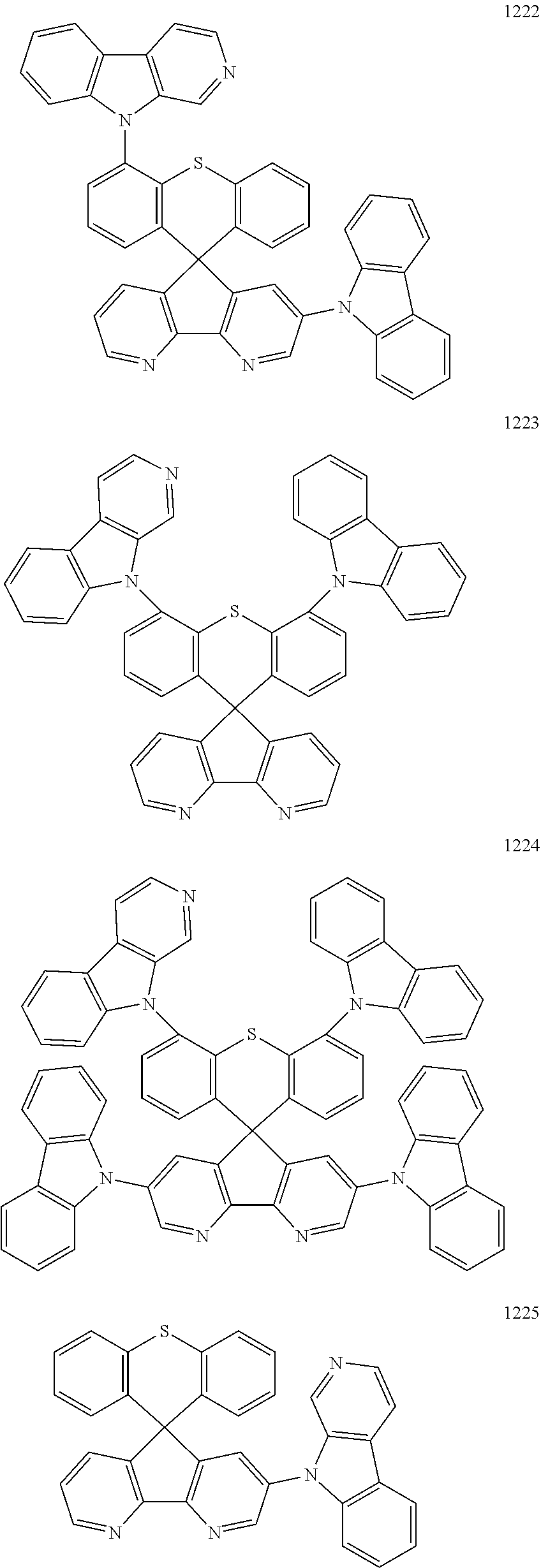
##STR00069## ##STR00070## ##STR00071## ##STR00072## ##STR00073## ##STR00074## ##STR00075## ##STR00076## ##STR00077## ##STR00078## ##STR00079## ##STR00080## ##STR00081## ##STR00082## ##STR00083## ##STR00084## ##STR00085## ##STR00086## ##STR00087## ##STR00088## ##STR00089## ##STR00090## ##STR00091## ##STR00092## ##STR00093## ##STR00094## ##STR00095## ##STR00096## ##STR00097## ##STR00098## ##STR00099## ##STR00100## ##STR00101## ##STR00102## ##STR00103## ##STR00104## ##STR00105## ##STR00106## ##STR00107## ##STR00108## ##STR00109## ##STR00110## ##STR00111## ##STR00112## ##STR00113## ##STR00114##
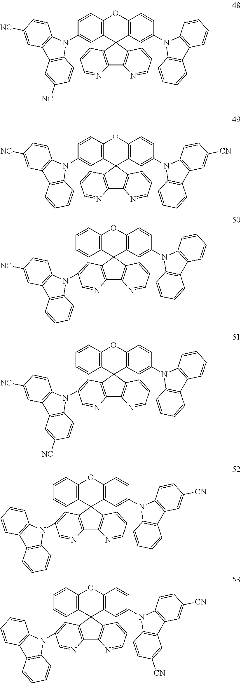
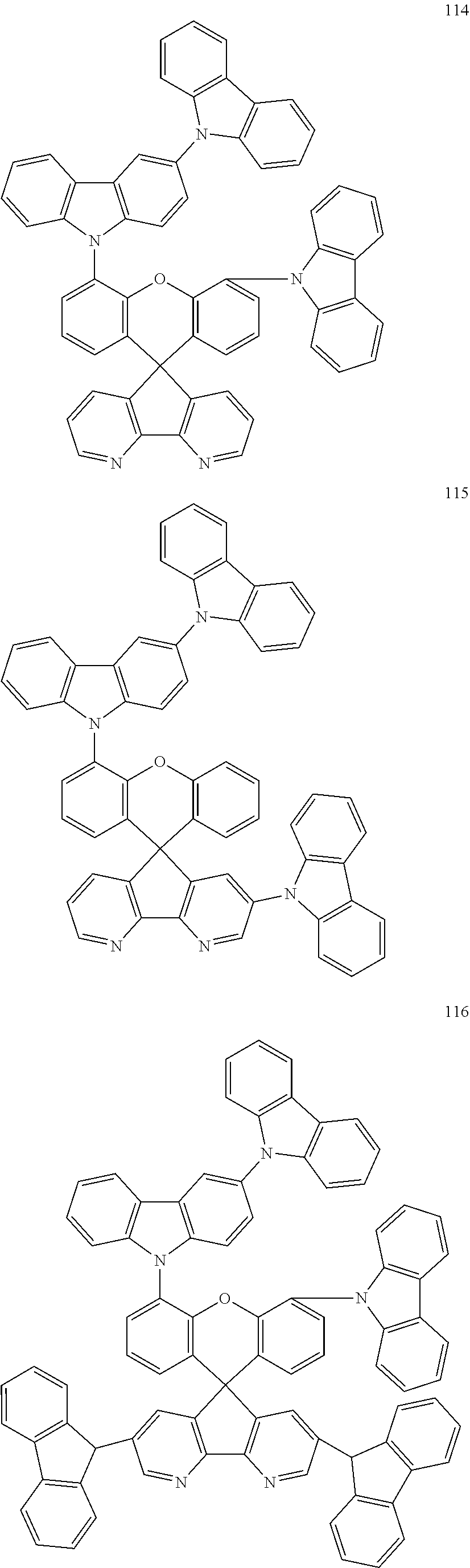
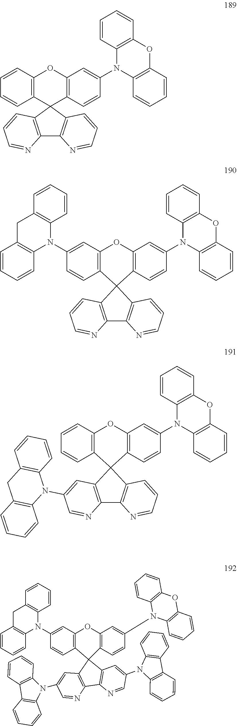
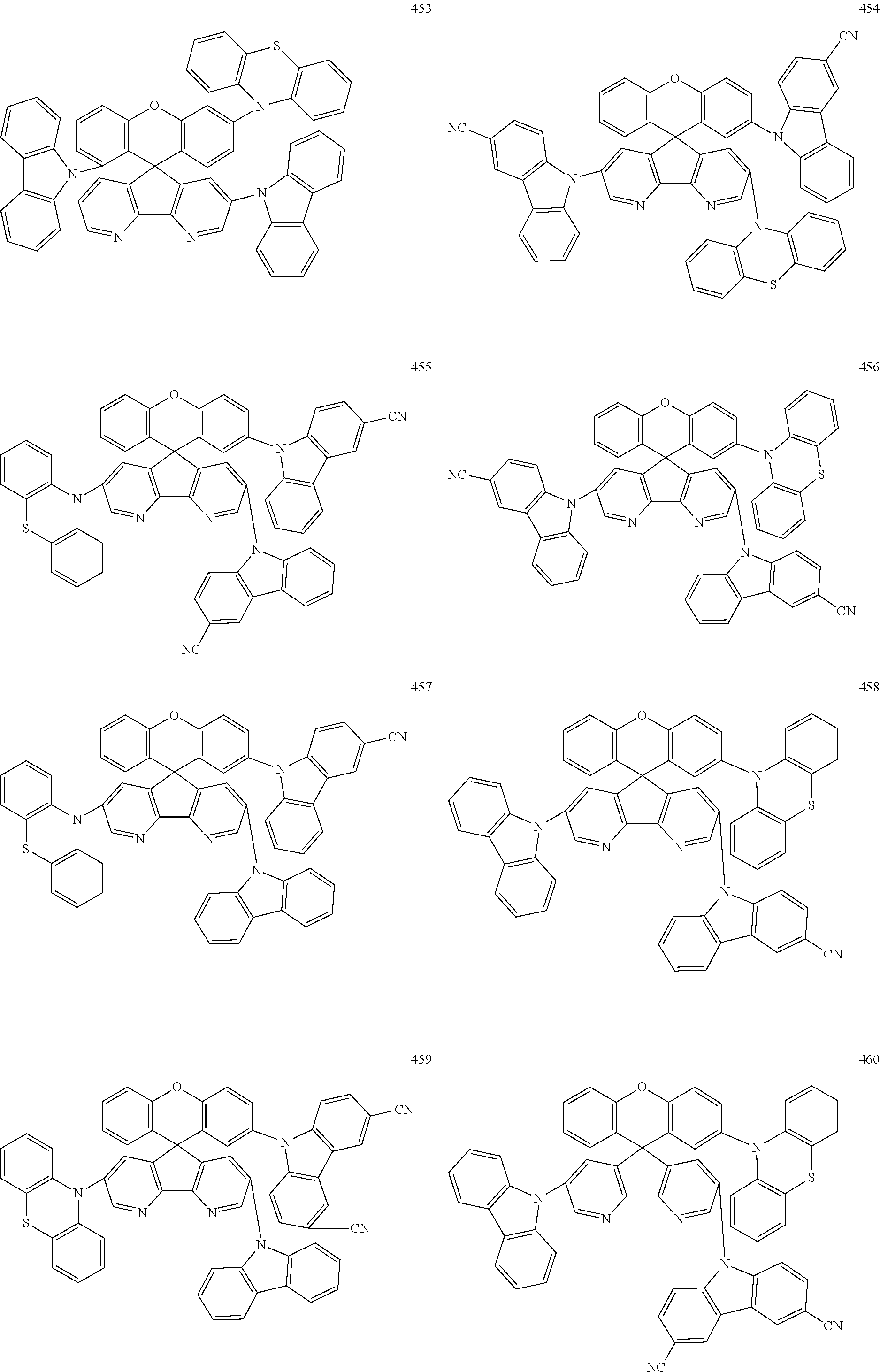
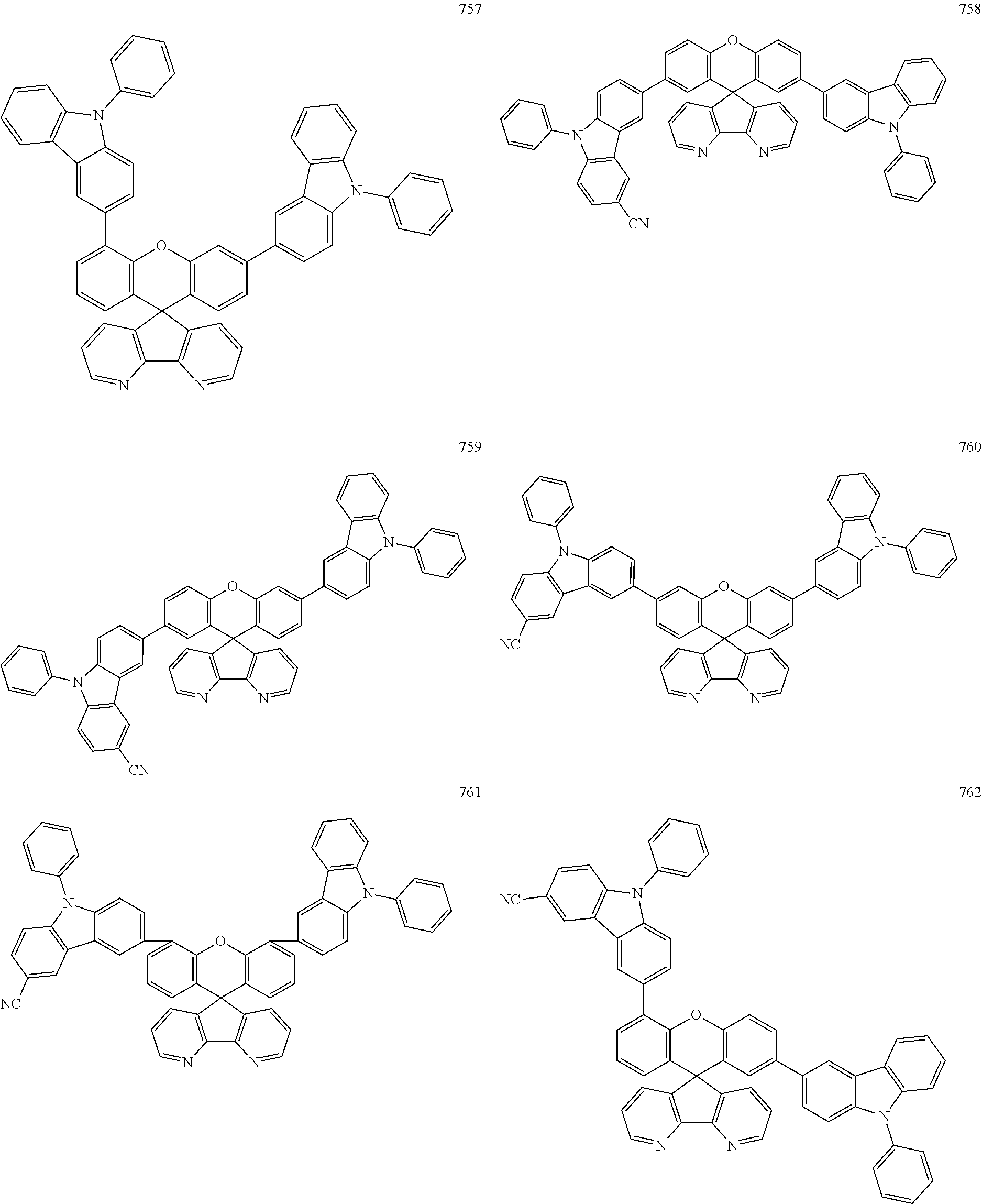
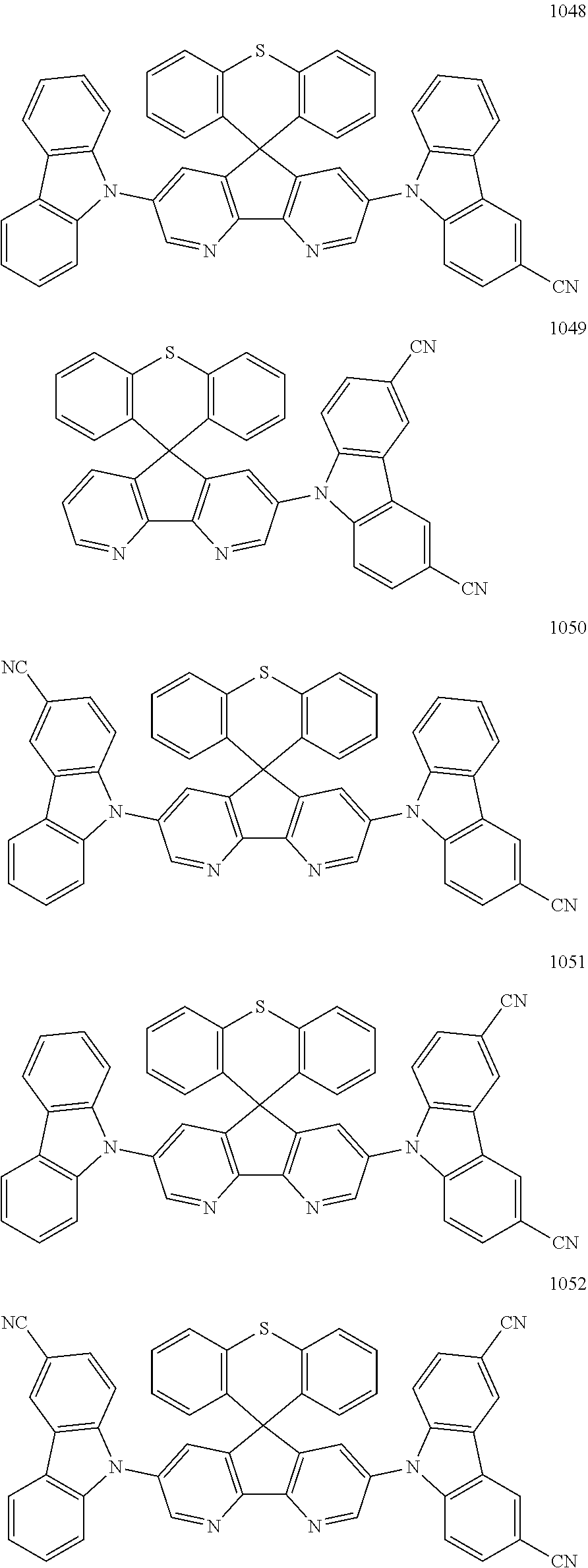
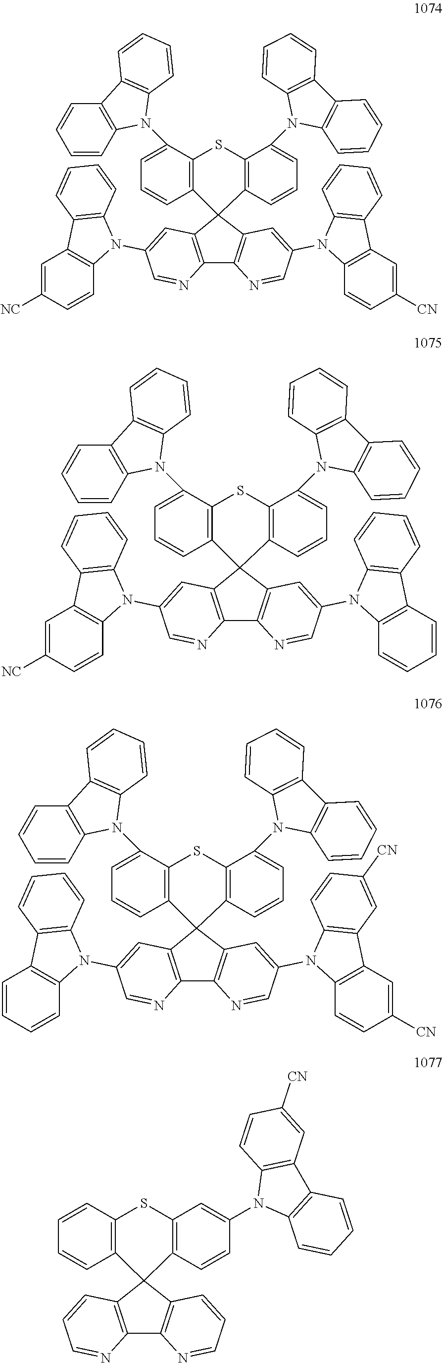
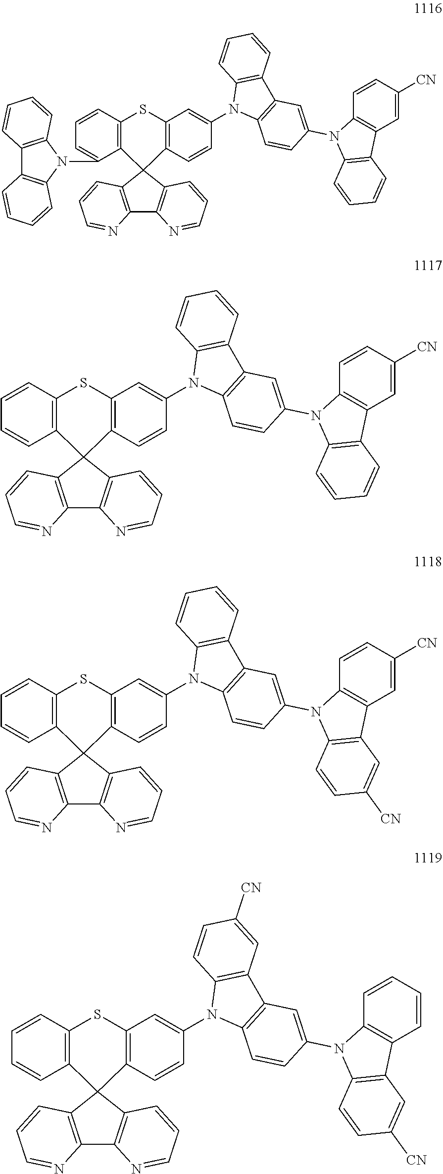
##STR00115## ##STR00116## ##STR00117## ##STR00118## ##STR00119## ##STR00120## ##STR00121## ##STR00122## ##STR00123## ##STR00124## ##STR00125## ##STR00126## ##STR00127## ##STR00128## ##STR00129## ##STR00130## ##STR00131## ##STR00132## ##STR00133## ##STR00134## ##STR00135## ##STR00136## ##STR00137## ##STR00138## ##STR00139## ##STR00140## ##STR00141## ##STR00142## ##STR00143## ##STR00144## ##STR00145## ##STR00146## ##STR00147## ##STR00148## ##STR00149## ##STR00150## ##STR00151## ##STR00152##
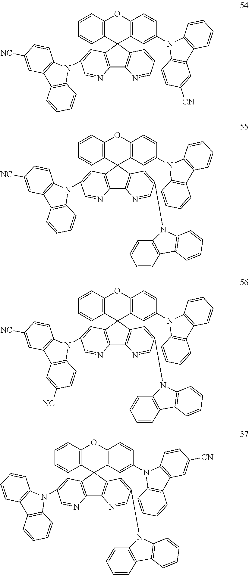
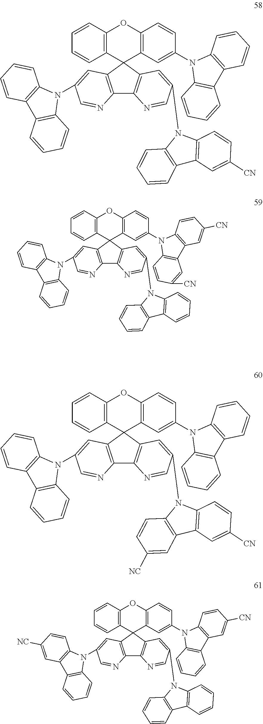
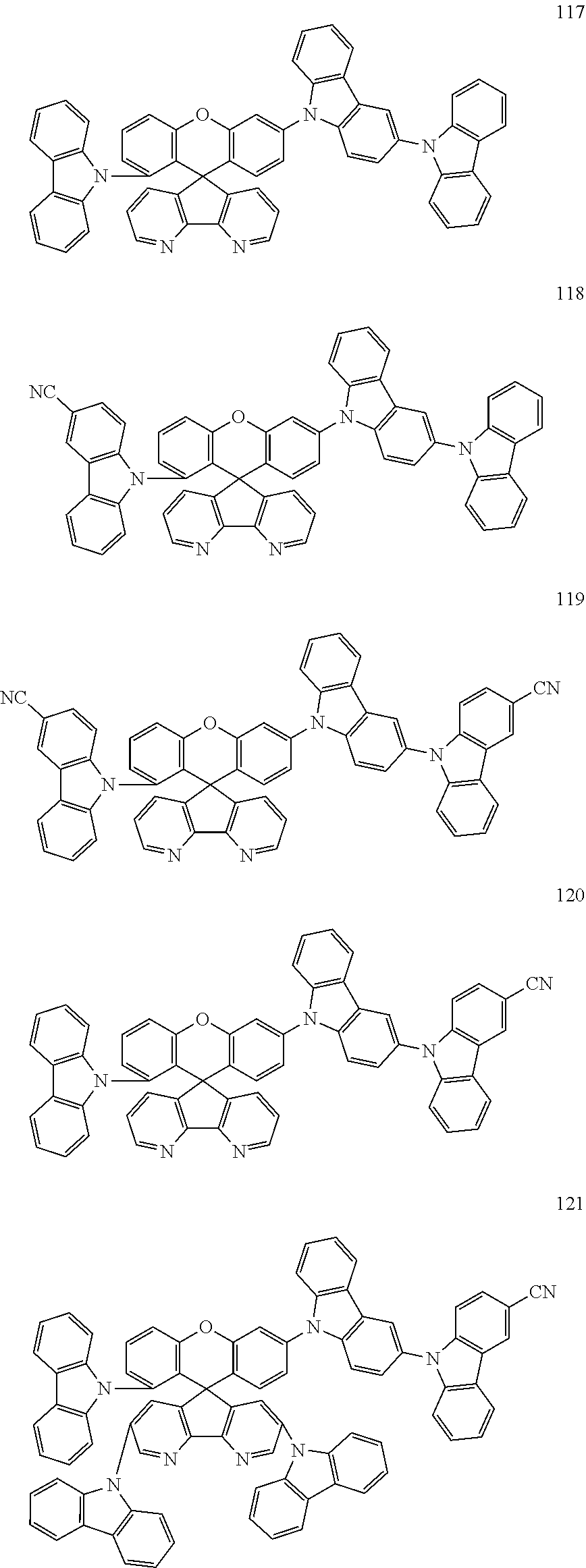
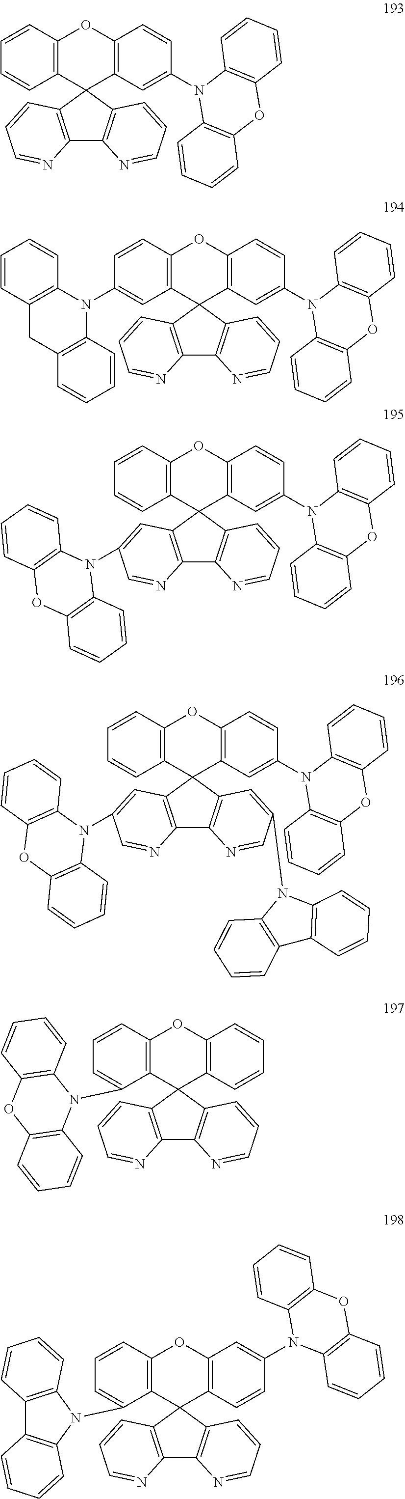
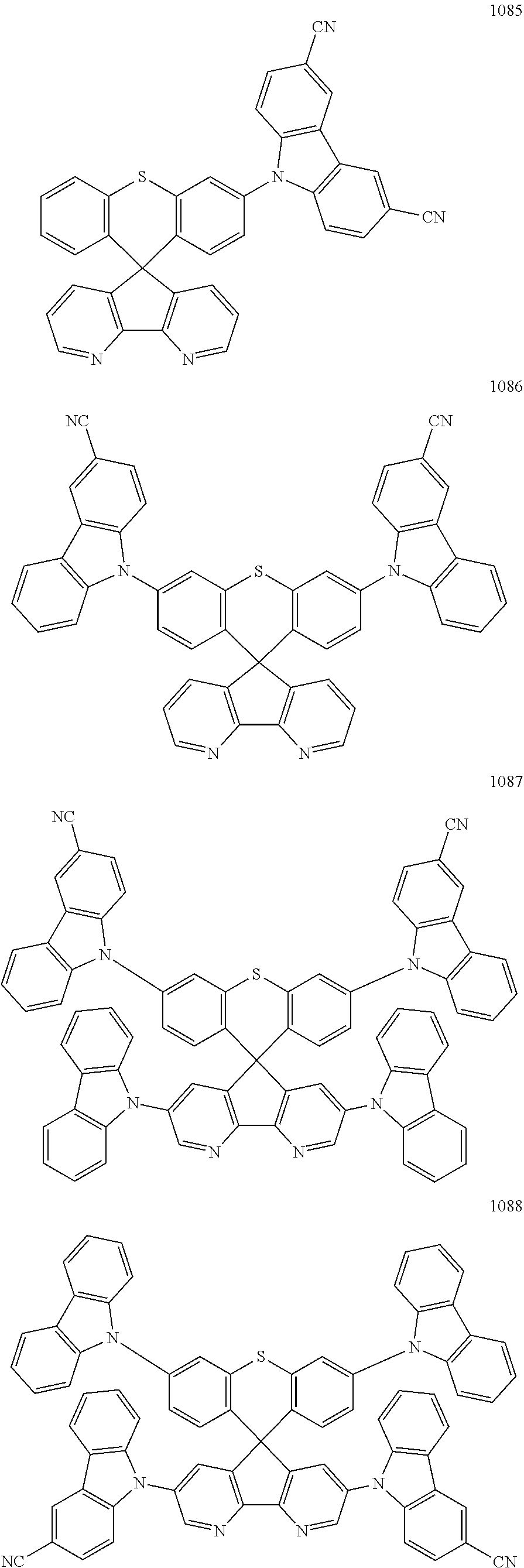
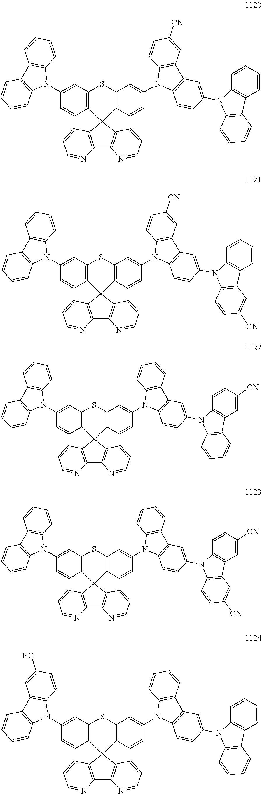
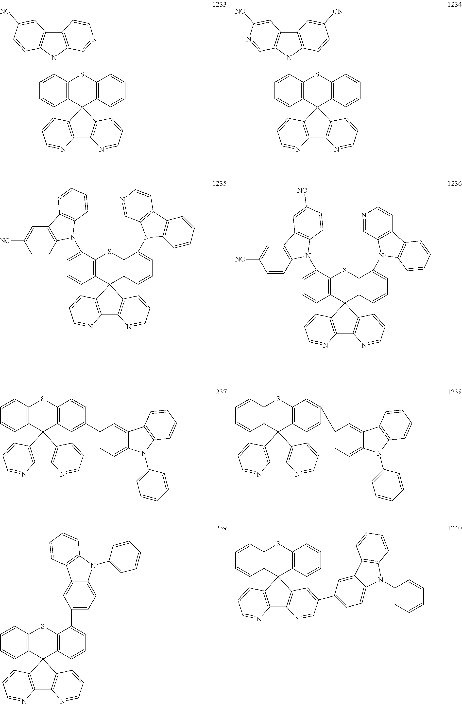
##STR00153## ##STR00154## ##STR00155## ##STR00156## ##STR00157## ##STR00158## ##STR00159## ##STR00160## ##STR00161## ##STR00162## ##STR00163## ##STR00164## ##STR00165## ##STR00166## ##STR00167## ##STR00168## ##STR00169## ##STR00170## ##STR00171## ##STR00172## ##STR00173## ##STR00174## ##STR00175## ##STR00176## ##STR00177## ##STR00178## ##STR00179## ##STR00180## ##STR00181## ##STR00182## ##STR00183## ##STR00184## ##STR00185## ##STR00186## ##STR00187## ##STR00188## ##STR00189## ##STR00190## ##STR00191## ##STR00192## ##STR00193## ##STR00194## ##STR00195## ##STR00196## ##STR00197## ##STR00198## ##STR00199## ##STR00200## ##STR00201## ##STR00202## ##STR00203## ##STR00204## ##STR00205## ##STR00206## ##STR00207## ##STR00208##
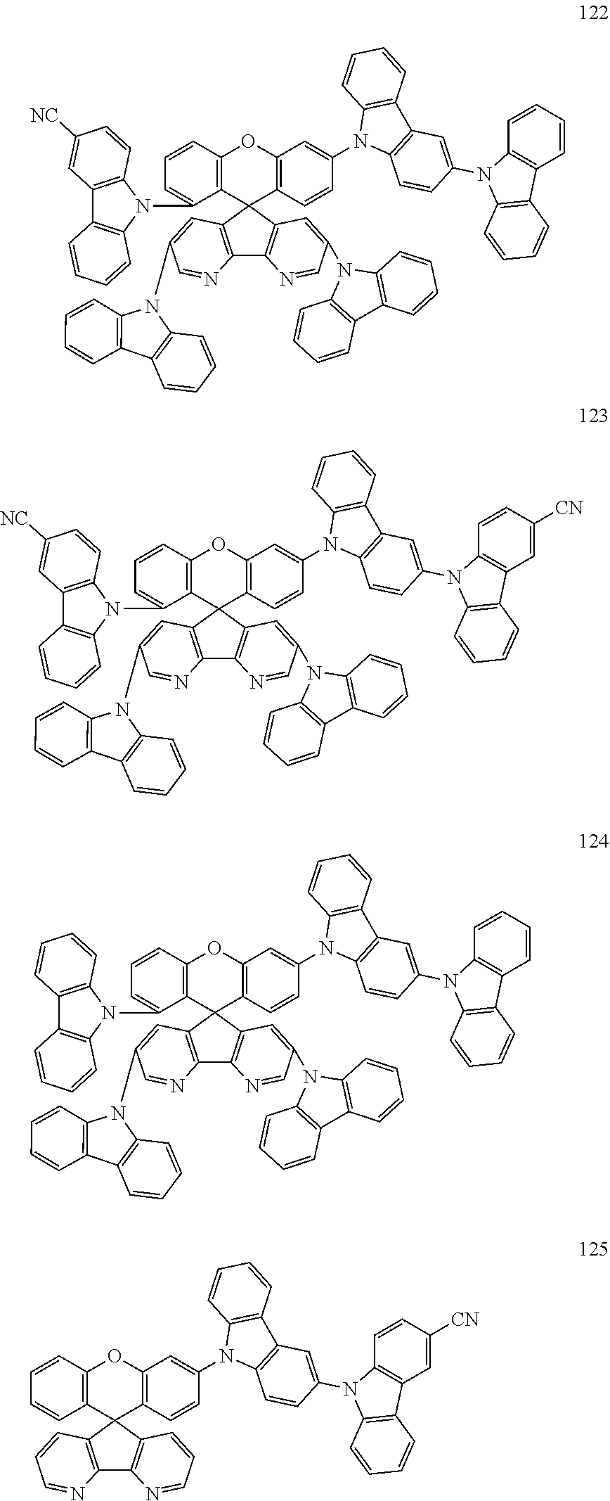
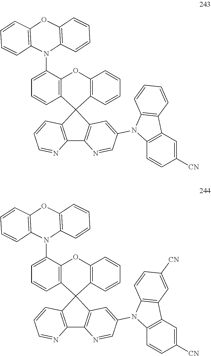
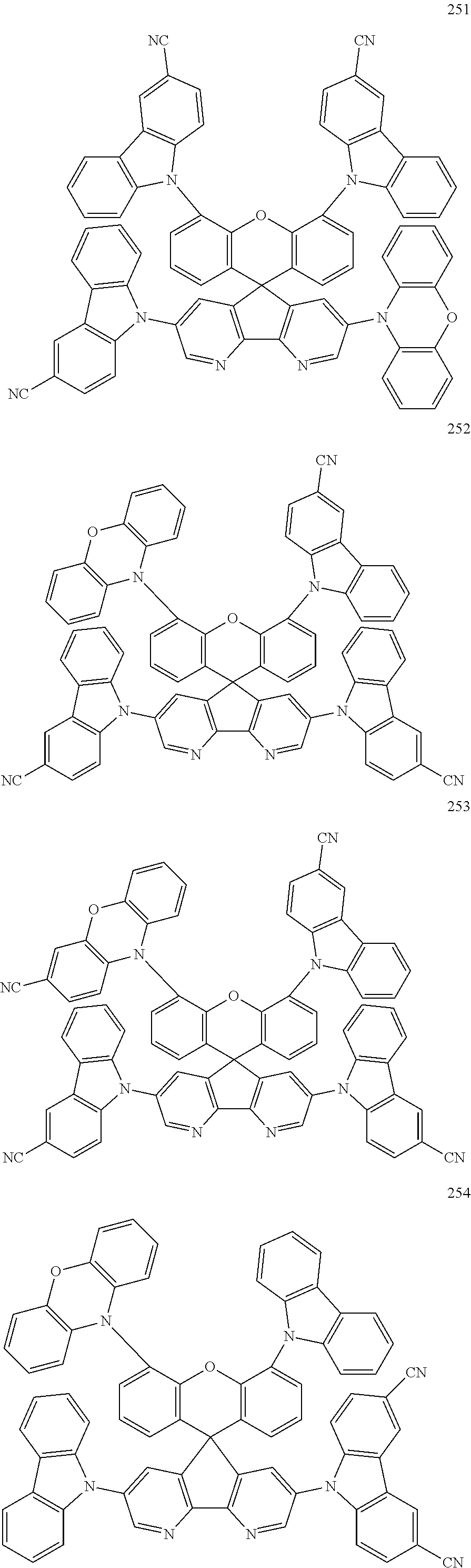
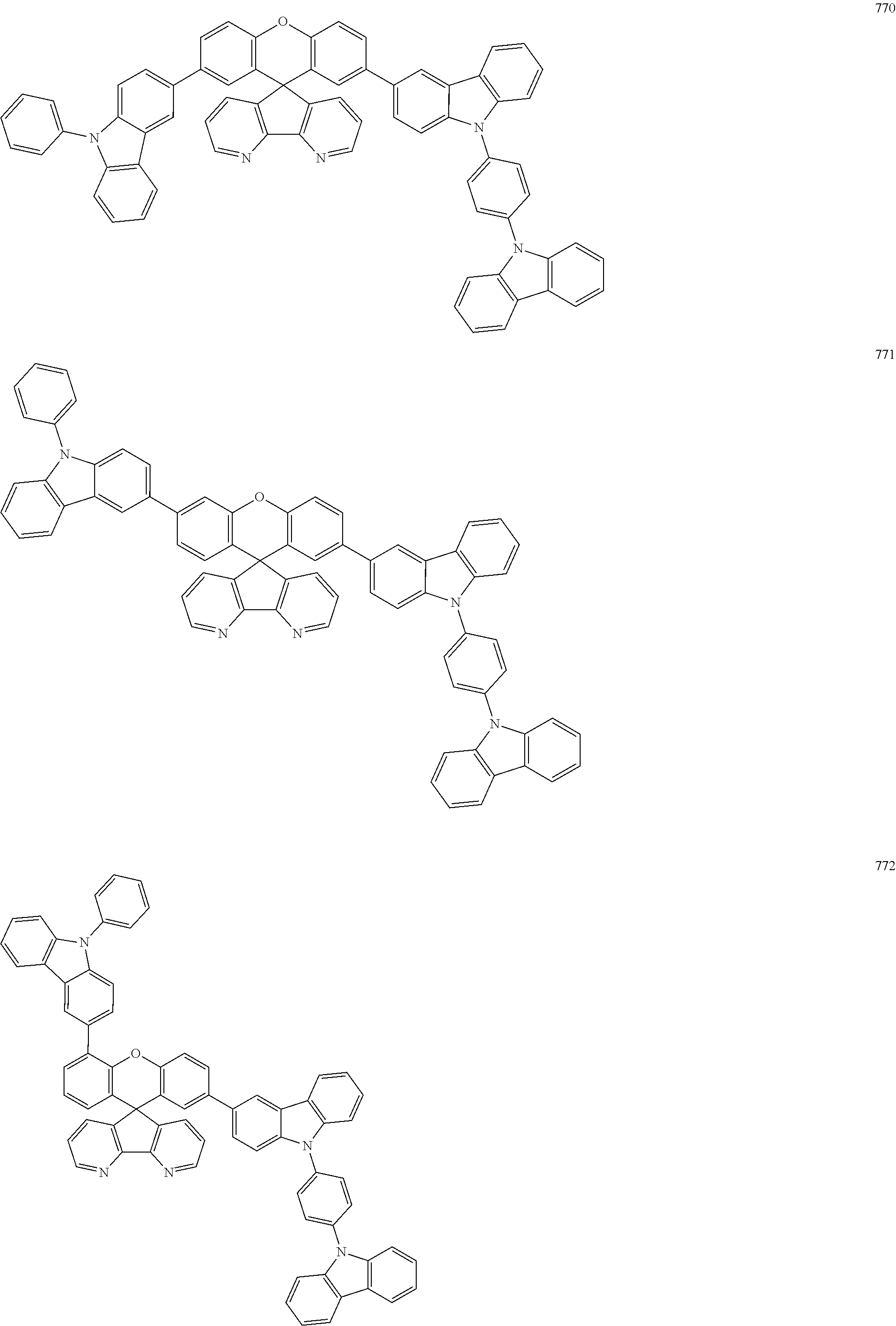
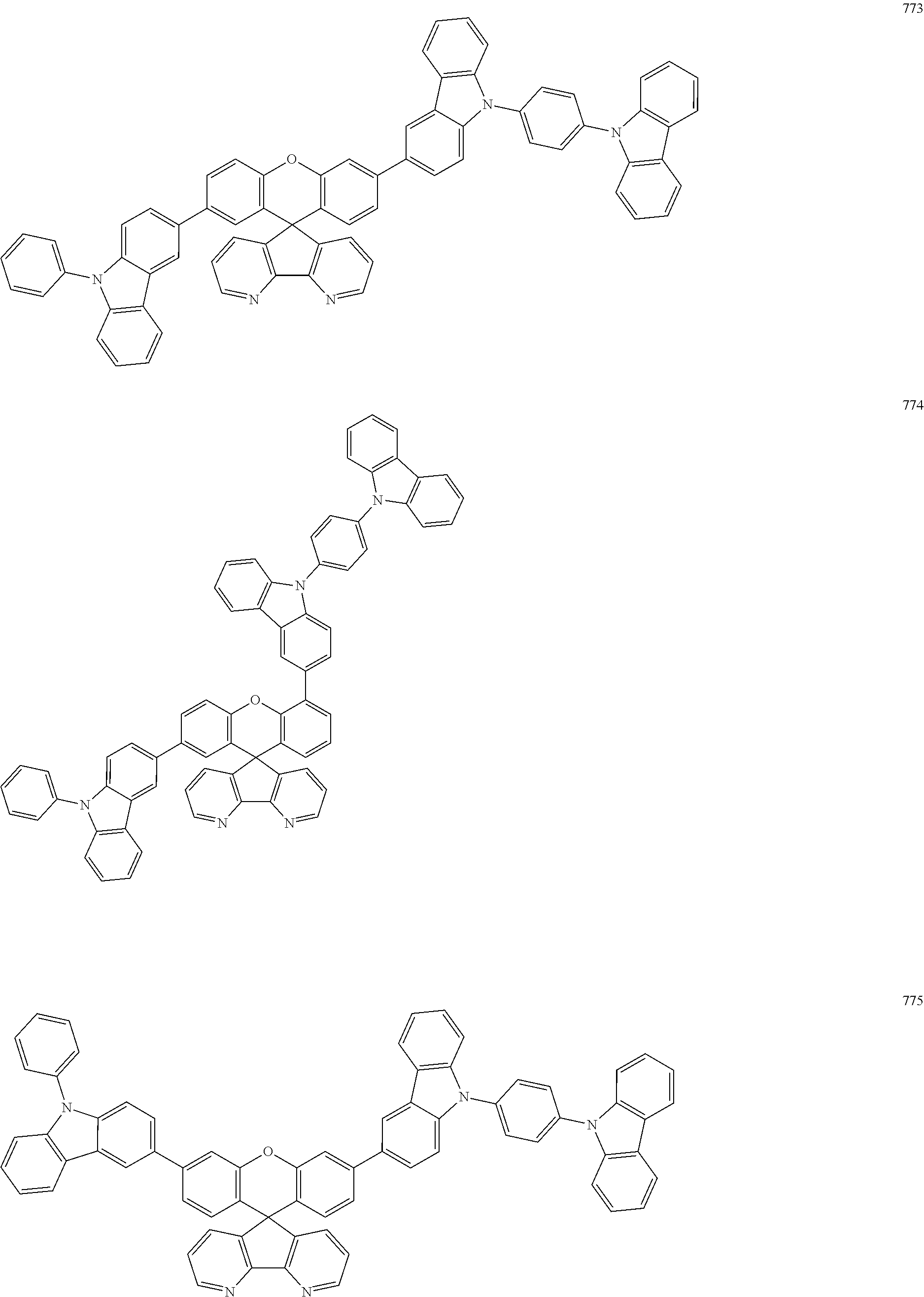
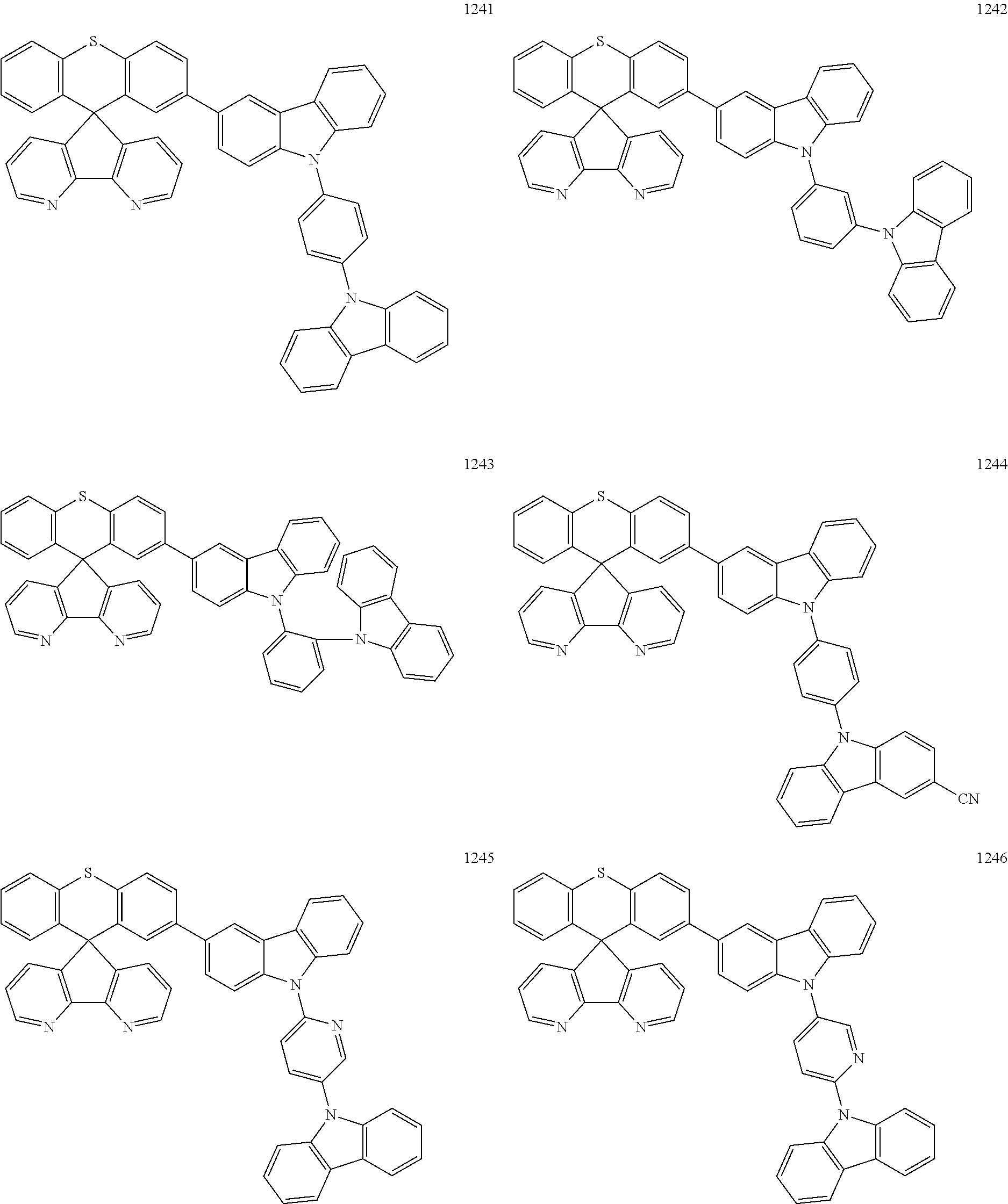
##STR00209## ##STR00210## ##STR00211## ##STR00212## ##STR00213## ##STR00214## ##STR00215## ##STR00216## ##STR00217## ##STR00218## ##STR00219## ##STR00220## ##STR00221## ##STR00222## ##STR00223## ##STR00224## ##STR00225## ##STR00226## ##STR00227## ##STR00228## ##STR00229## ##STR00230## ##STR00231## ##STR00232## ##STR00233## ##STR00234## ##STR00235## ##STR00236## ##STR00237## ##STR00238## ##STR00239## ##STR00240## ##STR00241## ##STR00242## ##STR00243## ##STR00244## ##STR00245## ##STR00246## ##STR00247## ##STR00248## ##STR00249## ##STR00250## ##STR00251## ##STR00252## ##STR00253## ##STR00254## ##STR00255## ##STR00256## ##STR00257## ##STR00258##
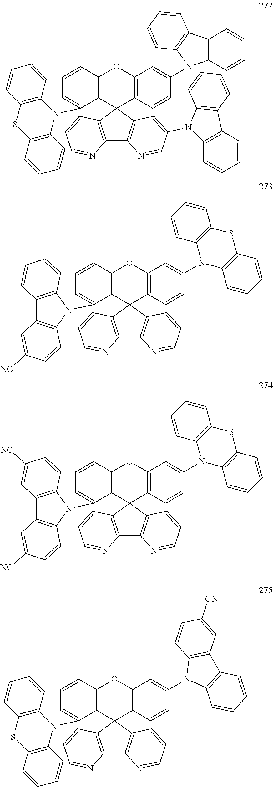
##STR00259## ##STR00260## ##STR00261## ##STR00262## ##STR00263## ##STR00264## ##STR00265## ##STR00266## ##STR00267## ##STR00268## ##STR00269## ##STR00270## ##STR00271## ##STR00272## ##STR00273## ##STR00274## ##STR00275## ##STR00276## ##STR00277## ##STR00278## ##STR00279## ##STR00280## ##STR00281## ##STR00282## ##STR00283## ##STR00284## ##STR00285## ##STR00286## ##STR00287## ##STR00288## ##STR00289## ##STR00290## ##STR00291## ##STR00292## ##STR00293## ##STR00294## ##STR00295## ##STR00296## ##STR00297## ##STR00298## ##STR00299##
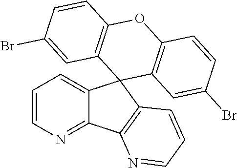
[0044] In an embodiment of the present disclosure, the compound of Formula 1 may be one of Formula 23. The compound of the present disclosure may include a diazafluorene core such that a high T1 value is provided. As a result, properties of high emitting efficiency, long lifespan and low driving voltage are provided.
##STR00300## ##STR00301## ##STR00302##
[0045] The compound of the present disclosure may be an organic emitting material providing fluorescent emission or delayed fluorescent emission. Accordingly, the compound of the present disclosure may be used for the OLED.
[0046] FIG. 1 is a schematic cross-sectional view of an organic light emitting display device according to the present disclosure.
[0047] As shown in FIG. 1, the organic light emitting display device 100 includes a substrate 110, a TFT Tr and an OLED (organic light emitting diode) D connected to the TFT Tr.
[0048] The substrate 110 may be a glass substrate or a plastic substrate. For example, the substrate 110 may be a polyimide substrate.
[0049] A buffer layer 120 is formed on the substrate, and the TFT Tr is formed on the buffer layer 120. The buffer layer 120 may be omitted.
[0050] A semiconductor layer 122 is formed on the buffer layer 120. The semiconductor layer 122 may include an oxide semiconductor material or polycrystalline silicon.
[0051] When the semiconductor layer 122 includes the oxide semiconductor material, a light-shielding pattern (not shown) may be formed under the semiconductor layer 122. The light to the semiconductor layer 122 is shielded or blocked by the light-shielding pattern such that thermal degradation of the semiconductor layer 122 can be prevented. On the other hand, when the semiconductor layer 122 includes polycrystalline silicon, impurities may be doped into both sides of the semiconductor layer 122.
[0052] A gate insulating layer 124 is formed on the semiconductor layer 122. The gate insulating layer 124 may be formed of an inorganic insulating material such as silicon oxide or silicon nitride.
[0053] A gate electrode 130, which is formed of a conductive material, e.g., metal, is formed on the gate insulating layer 124 to correspond to a center of the semiconductor layer 122.
[0054] In FIG. 1, the gate insulating layer 124 is formed on an entire surface of the substrate 110. Alternatively, the gate insulating layer 124 may be patterned to have the same shape as the gate electrode 130.
[0055] An interlayer insulating layer 132, which is formed of an insulating material, is formed on the gate electrode 130. The interlayer insulating layer 132 may be formed of an inorganic insulating material, e.g., silicon oxide or silicon nitride, or an organic insulating material, e.g., benzocyclobutene or photo-acryl.
[0056] The interlayer insulating layer 132 includes first and second contact holes 134 and 136 exposing both sides of the semiconductor layer 122. The first and second contact holes 134 and 136 are positioned at both sides of the gate electrode 130 to be spaced apart from the gate electrode 130.
[0057] The first and second contact holes 134 and 136 are formed through the gate insulating layer 124. Alternatively, when the gate insulating layer 124 is patterned to have the same shape as the gate electrode 130, the first and second contact holes 134 and 136 is formed only through the interlayer insulating layer 132.
[0058] A source electrode 140 and a drain electrode 142, which are formed of a conductive material, e.g., metal, are formed on the interlayer insulating layer 132.
[0059] The source electrode 140 and the drain electrode 142 are spaced apart from each other with respect to the gate electrode 130 and respectively contact both sides of the semiconductor layer 122 through the first and second contact holes 134 and 136.
[0060] The semiconductor layer 122, the gate electrode 130, the source electrode 140 and the drain electrode 142 constitute the TFT Tr. The TFT Tr serves as a driving element.
[0061] In the TFT Tr, the gate electrode 130, the source electrode 140, and the drain electrode 142 are positioned over the semiconductor layer 122. Namely, the TFT Tr has a coplanar structure.
[0062] Alternatively, in the TFT Tr, the gate electrode may be positioned under the semiconductor layer, and the source and drain electrodes may be positioned over the semiconductor layer such that the TFT Tr may have an inverted staggered structure. In this instance, the semiconductor layer may include amorphous silicon.
[0063] Although not shown, a gate line and a data line cross each other to define a pixel region, and a switching TFT is formed to be connected to the gate and data lines. The switching TFT is connected to the TFT Tr as the driving element.
[0064] In addition, a power line, which may be formed to be parallel to and spaced apart from one of the gate and data lines, and a storage capacitor for maintaining the voltage of a gate electrode of the TFT Tr in one frame may be further formed.
[0065] A passivation layer 150, which includes a drain contact hole 152 exposing the drain electrode 142 of the TFT Tr, is formed to cover the TFT Tr.
[0066] A first electrode 160, which is connected to the drain electrode 142 of the TFT Tr through the drain contact hole 152, is separately formed in each pixel region. The first electrode 160 may be an anode, i.e., a hole injection electrode, and may be formed of a conductive material having a relatively high work function. For example, the first electrode 160 may be formed of a transparent conductive material such as indium-tin-oxide (ITO), indium-zinc-oxide (IZO) or graphene.
[0067] When the organic light emitting display device 100 is operated in a top-emission type, a reflection electrode or a reflection layer may be formed under the first electrode 160. For example, the reflection electrode or the reflection layer may be formed of aluminum-palladium-copper (APC) alloy.
[0068] A bank layer 166 is formed on the passivation layer 150 to cover an edge of the first electrode 160. Namely, the bank layer 166 is positioned at a boundary of the pixel region and exposes a center of the first electrode 160 in the pixel region.
[0069] An organic material layer (emitting layer) 162 is formed on the first electrode 160. The organic material layer 162 may have a single-layered structure of an emitting material layer (EML) including the organic emitting compound. To increase an emitting efficiency of the OLED device, the organic material layer 162 may have a multi-layered structure.
[0070] A second electrode 164 is formed over the substrate 110 where the organic emitting layer 162 is formed. The second electrode 164 covers an entire surface of the display area and may be formed of a conductive material having a relatively low work function to serve as a cathode, i.e., an electron injection electrode. For example, the second electrode 164 may be formed of aluminum (Al), magnesium (Mg), Al--Mg alloy (AlMg), gold (Au) or silver (Ag).
[0071] The first electrode 160, the organic emitting layer 162 and the second electrode 164 constitute the OLED D.
[0072] An encapsulation film 170 is formed on the second electrode 164 to prevent penetration of moisture into the OLED D. The encapsulation film 170 includes a first inorganic insulating layer 172, an organic insulating layer 174 and a second inorganic insulating layer 176 sequentially stacked, but it is not limited thereto. The encapsulation film 170 may be omitted.
[0073] A polarization plate (not shown) for reducing an ambient light reflection may be disposed on the encapsulation film 170 of the top-emission type OLED D. For example, the polarization plate may be a circular polarization plate.
[0074] In addition, a cover window (not shown) may be attached to the encapsulation film 170 or the polarization plate. In this instance, the substrate 110 and the cover window have a flexible property such that a flexible display device may be provided.
[0075] The organic material layer 162 includes the compound of the present disclosure.
[0076] The compound of the present disclosure may be included in the emitting material layer, but it is not limited thereto. In addition, the compound of the present disclosure may be used alone or in combination with known compounds when forming the organic material layer 162.
[0077] FIG. 2 is a schematic cross-sectional view of an OLED according to a first embodiment of the present disclosure.
[0078] As shown in FIG. 2, the OLED D includes the first and second electrodes 160 and 164, which face each other, and the organic emitting layer 162 therebetween. The organic emitting layer 162 includes an emitting material layer (EML) 240 between the first and second electrodes 160 and 164, a hole transporting layer (HTL) 220 between the first electrode 160 and the EML 240 and an electron transporting layer (ETL) 260 between the second electrode 164 and the EML 240.
[0079] In addition, the organic emitting layer 162 may further include a hole injection layer (HIL) 210 between the first electrode 160 and the HTL 220 and an electron injection layer (EIL) 270 between the second electrode 164 and the ETL 260.
[0080] Moreover, the organic emitting layer 162 may further include an electron blocking layer (EBL) 230 between the HTL 220 and the EML 240 and a hole blocking layer (HBL) 250 between the EML 240 and the ETL 260.
[0081] For example, each of the hole injection layer 210, the hole transporting layer 220, the electron blocking layer 230, the emitting material layer 240, the hole blocking layer 250, the electron transporting layer 260, the electron injection layer 270 may be formed by a vacuum deposition method, a spin coating method, a casting method, or a Langmuir-Blodgett (LB) method. Each of the above layers may be deposited under the deposition temperature of about 50-500.degree. C., the degree of vacuum of about 10.sup.-8 to 10.sup.-3 torr and the deposition rate of about 0.01 to 100 .ANG./sec to have a thickness of about 10 .ANG. to 5 .mu.m.
[0082] The hole injection layer 210, the hole transporting layer 220, the emitting material layer 240, the electron transporting layer 260 of the organic light emitting device may use the compound of the present disclosure or may use the following materials. In addition, the compounds according to the present disclosure can be used together with known materials.
##STR00303##
[0083] At least one of the hole injection layer 210, the hole transporting layer 220, the electron blocking layer 230, the emitting material layer 240, the hole blocking layer 250, the electron transporting layer 260 and the electron injection layer 270 may include the compound of the present disclosure.
[0084] For example, the emitting material layer 240 may include the compound of the present disclosure. The emitting material layer 240 may include only the compound. Alternatively, the emitting material layer 240 may further include a known compound as a host or a dopant. In this case, the compound of the present disclosure is used as a dopant or a host.
[0085] For example, when the compound of the present disclosure is used as a dopant, the emitting material layer 240 further includes a host. In this instance, the excited singlet energy level of the host is higher (greater) than that of the compound of the present disclosure, or the excited triplet energy level of the host is higher than that of the compound of the present disclosure. In addition, the compound of the present disclosure may have a weight % of about 1 to 40 with respect to the host.
[0086] In the emitting material layer 240, the compound of the present disclosure may be used as a first dopant (assistance dopant), and a second dopant may be further included. In this case, the emitting material layer 240 may provide dark blue emission.
[0087] On the other hand, in the emitting material layer 240, the compound of the present disclosure may be used as a host, and a dopant may be further included. The dopant has a weight % of about 1 to 40 with respect to the compound of the present disclosure as the host. In this case, the dopant may be at least one of a delayed fluorescent dopant (delayed fluorescent compound), a fluorescent dopant (fluorescent compound) and a phosphorescent dopant (phosphorescent compound).
[0088] For example, when the emitting material layer 240 includes a host, which is the compound of the present disclosure, and a delayed fluorescent dopant, a difference (|HOMO.sub.Host-HOMO.sub.Dopant|) between the HOMO level (HOMO.sub.Host) of the host and the HOMO level (HOMO.sub.Dopant) of the delayed fluorescent dopant or a difference (|LUMO.sub.Host-LUMO.sub.Dopant|) between the LUMO level (LUMO.sub.Host) of the host and the LUMO level (LUMO.sub.Dopant) of the dopant is 0.5 eV. As a result, the charge transfer efficiency from the host to the delayed fluorescent dopant is improved.
[0089] The energy level of triplet state of the delayed fluorescent dopant is smaller (lower) than the energy level of triplet state of the host, and a difference between the energy level of singlet state of the delayed fluorescent dopant and the energy level of triplet state of the delayed fluorescent dopant is equal to less than 0.3 eV. (.DELTA.E.sub.ST.ltoreq.0.3 eV) As the difference ".DELTA.E.sub.ST" is smaller, the emitting efficiency is higher. In addition, even if the difference ".DELTA.E.sub.ST" between the energy level of singlet state of the delayed fluorescent dopant and the energy level of triplet state of the delayed fluorescent dopant is about 0.3 eV, which is relatively large, the excitons in the singlet state and the excitons in the triplet state can be transited into the intermediate state.
[0090] On the other hand, the emitting material layer 240 may include the compound of the present disclosure as a host, a delayed fluorescent dopant (first dopant) and a fluorescent dopant (second dopant). The sum of the first and second dopants may be about 1 to 40 wt % with respect to the host.
[0091] In this case, the energy level of singlet state of the first dopant is greater than that of the second dopant. In addition, the energy level of triplet state of the first dopant is smaller than that of the host and greater than that of the second dopant.
[0092] When the emitting material layer 240 includes the host and the first and second dopant, the emission efficiency and the color sense may be further improved. Namely, since the energy transfer occurs from the host to the first dopant, the singlet energy and triplet energy of the first dopant are transferred to the second dopant, the light emission occurs in the second dopant. As a result, the quantum efficiency of the organic light emitting device D is increased, and the full width at half maximum (FWHM) is narrowed.
[0093] The first dopant with delayed fluorescence property has high quantum efficiency. However, since the first dopant has wide FWHM, the first dopant provides poor color purity. The second dopant with fluorescence property has narrow FWHM and an advantage in the color purity. However, the triplet exciton of the second dopant is not involved in the light emission such that the second dopant has low quantum efficiency.
[0094] However, when the emitting material layer 240 includes the first dopant, which is a delayed fluorescent material, and the second dopant, which is a fluorescent material, there are advantages in both emitting efficiency and color purity.
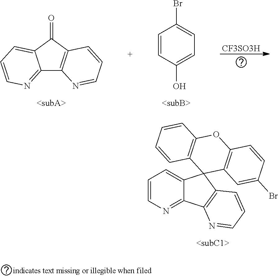
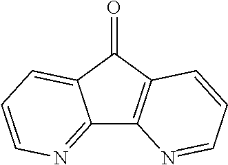
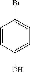
[0095] [Synthesis]
[0096] In one embodiment of the present disclosure, the intermediate SubC may be synthesized as follows, but it is not limited thereto.
##STR00304##
[0097] Synthesis of the Compound "subC1"
##STR00305##
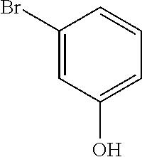
[0098] In the rounded-bottom flask, 4,5-diazafluorenone (subA, 5 g), 4-Bromophenol (subB, 7.3 g) and trifluoromethanesulfonic acid (5.5 g) were dissolved in toluene (50 ml), and the mixture was refluxed and stirred. The reaction was confirmed by thin layer chromatography (TLC), and the reaction was terminated after adding water. The organic layer was extracted with methylene chloride (MC) was filtered under reduced pressure. The column purification process and the recrystallization process were performed to the mixture the compound "subC1" (2'-bromospiro[cyclopenta[1,2-b:5,4-b']dipyridine-5,9'-xanthene], 6.4 g, 50% yield) was obtained.
[0099] Compounds "SubC2" to "SubC10" were synthesized by varying starting materials "SubA" and "SubB" as shown in Table 1 with synthesis of the compound "SubC1". (Y=yield)
TABLE-US-00001 TABLE 1 Y Sub A Sub B Sub C (%) Sub C1 ##STR00306## ##STR00307## ##STR00308## 50 Sub C2 ##STR00309## ##STR00310## ##STR00311## 52 Sub C3 ##STR00312## ##STR00313## ##STR00314## 55 Sub C4 ##STR00315## ##STR00316## ##STR00317## 49 Sub C5 ##STR00318## ##STR00319## ##STR00320## 44 Sub C6 ##STR00321## ##STR00322## ##STR00323## 60 Sub C7 ##STR00324## ##STR00325## ##STR00326## 48 Sub C8 ##STR00327## ##STR00328## ##STR00329## 54 Sub C9 ##STR00330## ##STR00331## ##STR00332## 45 Sub C10 ##STR00333## ##STR00334## ##STR00335## 43
[0100] The compounds of the present disclosure may be synthesized as follows, but it is not limited thereto.
##STR00336##
[0101] Synthesis of the Compound "A"
##STR00337##
[0102] In the rounded-bottom flask, 2'-bromospiro[cyclopenta[1,2-b:5,4-b']dipyridine-5,9'-xanthene] (SubC1, 5 g), carbazole (SubD, 3 g), t-BuONa (2.3 g) and Pd(OAc).sub.2 (0.2 g) were dissolved in toluene (50 ml), and the mixture was refluxed and stirred. The reaction was confirmed by thin layer chromatography (TLC), and the reaction was terminated after adding water. The organic layer was extracted with methylene chloride (MC) and was filtered under reduced pressure. The column purification process and the recrystallization process were performed to the mixture such that the compound "A" (2'-(9H-carbazol-9-yl)-[cyclopenta[1,2-b:5,4-b']dipyridine-5,9'-xanthene]- , 6.4 g, 54% yield) was obtained.
[0103] Molecular Weight: 499.56; m/z: 499.17 (100.0%), 500.17 (39.2%), 501.18 (7.1%)
[0104] Synthesis of the Compound "B"
##STR00338##
[0105] In compound "B" was obtained by the above reaction with the same synthesis conditions of the compound "A." (59% yield)
[0106] Molecular Weight: 524.57; m/z: 524.16 (100.0%), 525.17 (39.2%), 526.17 (7.7%), 525.16 (1.5%), 527.17 (1.1%)
[0107] Synthesis of the Compound "C"
##STR00339##
[0108] In compound "C" was obtained by the above reaction with the same synthesis conditions of the compound "A." (62% yield)
[0109] Molecular Weight: 549.58; m/z: 549.16 (100.0%), 550.16 (41.9%), 551.17 (7.9%), 552.17 (1.1%)
[0110] Synthesis of the Compound "D"
##STR00340##
[0111] In compound "D" was obtained by the above reaction with the same synthesis conditions of the compound "A." (62% yield)
[0112] Molecular Weight: 541.64; m/z: 541.22 (100.0%), 542.22 (41.4%), 543.22 (8.9%), 542.21 (1.1%), 544.23 (1.1%)
[0113] Synthesis of the Compound "E"
##STR00341##
[0114] In compound "E" was obtained by the above reaction with the same synthesis conditions of the compound "A." (60% yield)
[0115] Molecular Weight: 665.78; m/z: 665.25 (100.0%), 666.25 (52.3%), 667.25 (14.0%), 668.26 (2.2%), 666.24 (1.1%)
[0116] Synthesis of the Compound "F"
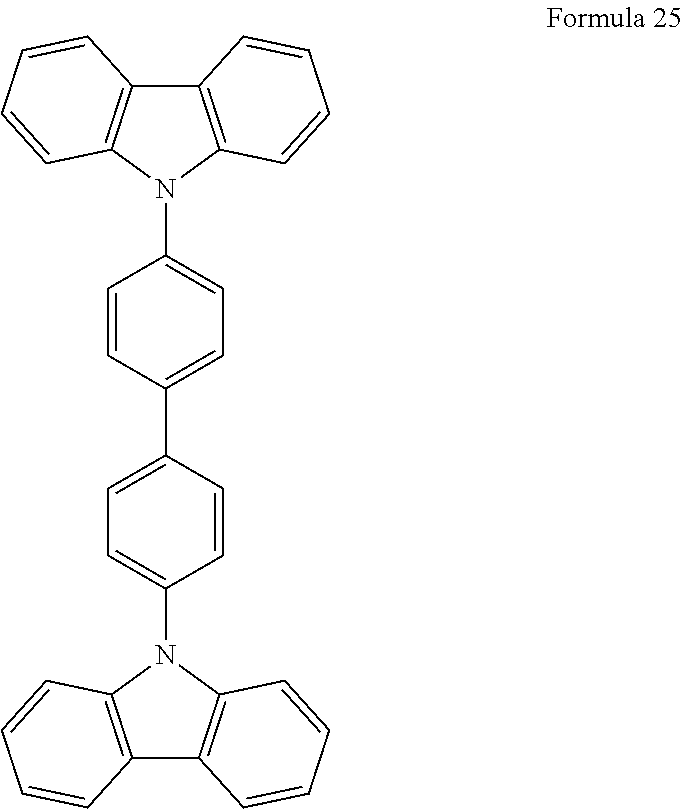
##STR00342##
[0117] In compound "F" was obtained by the above reaction with the same synthesis conditions of the compound "A." (65% yield)
[0118] Molecular Weight: 664.75; m/z: 664.23 (100.0%), 665.23 (51.2%), 666.23 (13.6%), 667.24 (2.1%), 665.22 (1.5%)
[0119] Synthesis of the Compound "G"
##STR00343##
[0120] In compound "G" was obtained by the above reaction with the same synthesis conditions of the compound "A." (66% yield)
[0121] Molecular Weight: 689.76; m/z: 689.22 (100.0%), 690.22 (53.8%), 691.23 (13.6%), 692.23 (2.6%)
[0122] Synthesis of the Compound "H"
##STR00344##
[0123] In compound "H" was obtained by the above reaction with the same synthesis conditions of the compound "A." (66% yield)
[0124] Molecular Weight: 500.55; m/z: 500.16 (100.0%), 501.17 (37.0%), 502.17 (6.9%), 501.16 (1.5%)
[0125] Synthesis of the Compound "I"
##STR00345##
[0126] In compound "I" was obtained by the above reaction with the same synthesis conditions of the compound "A." (62% yield)
[0127] m/z: 918.32 (100.0%), 919.32 (64.3%), 920.32 (21.0%), 921.33 (4.2%), 919.31 (1.5%)
[0128] Synthesis of the Compound "J"
##STR00346##
[0129] In compound "J" was obtained by the above reaction with the same synthesis conditions of the compound "A." (63% yield)
[0130] Molecular Weight: 714.77; m/z: 714.22 (100.0%), 715.22 (53.3%), 716.22 (15.2%), 717.23 (2.4%), 715.21 (2.2%)
[0131] Synthesis of the Compound "K"
##STR00347##
[0132] In compound "K" was obtained by the above reaction with the same synthesis conditions of the compound "A." (59% yield)
[0133] Molecular Weight: 764.79; m/z: 764.21 (100.0%), 765.21 (55.5%), 766.21 (16.8%), 765.20 (3.0%), 767.22 (2.7%)
[0134] Synthesis of the Compound "L"
##STR00348##
[0135] In compound "L" was obtained by the above reaction with the same synthesis conditions of the compound "A." (65% yield)
[0136] Molecular Weight: 748.91; m/z: 748.32 (100.0%), 749.32 (58.8%), 750.33 (16.4%), 751.33 (3.2%), 750.32 (1.1%)
[0137] Synthesis of the Compound "M"
##STR00349##
[0138] In compound "M" was obtained by the above reaction with the same synthesis conditions of the compound "A." (61% yield)
[0139] Molecular Weight: 997.19; m/z: 996.38 (100.0%), 997.39 (79.5%), 998.39 (31.4%), 999.39 (8.5%), 1000.40 (1.5%), 997.38 (1.5%), 998.38 (1.2%)
[0140] Synthesis of the Compound "N"
##STR00350##
[0141] In compound "N" was obtained by the above reaction with the same synthesis conditions of the compound "A." (58% yield)
[0142] Molecular Weight: 995.13; m/z: 994.34 (100.0%), 995.35 (77.3%), 996.35 (29.7%), 997.35 (8.2%), 995.34 (2.2%), 996.34 (1.7%), 998.36 (1.4%)
[0143] Synthesis of the Compound "O"
##STR00351##
[0144] In compound "O" was obtained by the above reaction with the same synthesis conditions of the compound "A." (59% yield)
[0145] Molecular Weight: 1045.15; m/z: 1044.33 (100.0%), 1045.34 (79.5%), 1046.34 (31.4%), 1047.34 (9.0%), 1045.33 (3.0%), 1046.33 (2.4%), 1048.35 (1.5%)
[0146] Synthesis of the Compound "P"
##STR00352##
[0147] In compound "P" was obtained by the above reaction with the same synthesis conditions of the compound "A." (56% yield)
[0148] Molecular Weight: 666.73; m/z: 666.22 (100.0%), 667.22 (49.0%), 668.22 (12.9%), 667.21 (2.2%), 669.23
[0149] Synthesis of the Compound "Q"
##STR00353##
[0150] In compound "Q" was obtained by the above reaction with the same synthesis conditions of the compound "A." (57% yield)
[0151] Molecular Weight: 499.56; m/z: 499.17 (100.0%), 500.17 (39.2%), 501.18 (7.1%)
[0152] Synthesis of the Compound "R"
##STR00354##
[0153] In compound "R" was obtained by the above reaction with the same synthesis conditions of the compound "A." (75% yield)
[0154] Molecular Weight: 524.57; m/z: 524.16 (100.0%), 525.17 (39.2%), 526.17 (7.7%), 525.16 (1.5%), 527.17 (1.1%)
[0155] Synthesis of the Compound "S"
##STR00355##
[0156] In compound "S" was obtained by the above reaction with the same synthesis conditions of the compound "A." (74% yield)
[0157] Molecular Weight: 541.64; m/z: 541.22 (100.0%), 542.22 (41.4%), 543.22 (8.9%), 542.21 (1.1%), 544.23 (1.1%)
[0158] Synthesis of the Compound "T"
##STR00356##
[0159] In compound "T" was obtained by the above reaction with the same synthesis conditions of the compound "A." (70% yield)
[0160] Molecular Weight: 665.78; m/z: 665.25 (100.0%), 666.25 (52.3%), 667.25 (14.0%), 668.26 (2.2%), 666.24 (1.1%)
[0161] Synthesis of the Compound "U"
##STR00357##
[0162] In compound "U" was obtained by the above reaction with the same synthesis conditions of the compound "A." (47% yield)
[0163] Molecular Weight: 664.75; m/z: 664.23 (100.0%), 665.23 (51.2%), 666.23 (13.6%), 667.24 (2.1%), 665.22 (1.5%)
[0164] Synthesis of the Compound "V"
##STR00358##
[0165] In compound "V" was obtained by the above reaction with the same synthesis conditions of the compound "A." (54% yield)
[0166] Molecular Weight: 714.77; m/z: 714.22 (100.0%), 715.22 (53.3%), 716.22 (15.2%), 717.23 (2.4%), 715.21 (2.2%)
[0167] Synthesis of the Compound "W"
##STR00359##
[0168] In compound "W" was obtained by the above reaction with the same synthesis conditions of the compound "A." (54% yield)
[0169] Molecular Weight: 748.91; m/z: 748.32 (100.0%), 749.32 (58.8%), 750.33 (16.4%), 751.33 (3.2%), 750.32 (1.1%)
[0170] Synthesis of the Compound "X"
##STR00360##
[0171] In compound "X" was obtained by the above reaction with the same synthesis conditions of the compound "A." (54% yield)
[0172] Molecular Weight: 997.19; m/z: 996.38 (100.0%), 997.39 (79.5%), 998.39 (31.4%), 999.39 (8.5%), 1000.40 (1.5%), 997.38 (1.5%), 998.38 (1.2%)
[0173] Synthesis of the Compound "Y"
##STR00361##
[0174] After the compound "SubC1" was dissolved in tetrahydrofuran/toluene (volume ratio=5:1), the compound "SubD25" (1.2 equivalent) was added. Potassium carbonate (4.4 equivalent) and Pd(0) (0.05 equivalent) dissolved in distilled water (DI water) were added. The reaction mixture was refluxed under the temperature of 80.degree. C. and stirred for 24 hrs. The reaction was confirmed by TLC, and the reaction was terminated. The organic layer was extracted with ethylene acetate (EA) and was filtered under reduced pressure. The column purification process and the recrystallization process were performed to the mixture such that the compound "Y" (51% yield) was obtained.
[0175] Molecular Weight: 740.85; m/z: 740.26 (100.0%), 741.26 (57.7%), 742.26 (17.2%), 743.27 (3.1%), 741.25 (1.5%)
[0176] [Delayed Fluorescent Type OLED]
[0177] (1) Example 1 (Ex1)
[0178] A glass substrate (ITO substrate) coated with indium-tin-oxide (ITO) with a thickness of 150 nm was washed by distilled water. After washing by the distilled water, the ITO substrate was ultrasonically washed with a solvent such as isopropyl alcohol, acetone or methanol and dried. The ITO substrate was transferred into a plasma cleaner, and then the ITO substrate was cleaned for 5 minutes using oxygen plasma. The hole injection layer with a thickness of 60 nm was formed on the ITO substrate by spin-coating PEDOT:PSS. The hole transporting layer (TAPC, 20 nm) and the electron blocking layer (mCP, 10 nm) were sequentially formed on the hole injection layer by using the thermal evaporator. The emitting material layer (EML) (mCP (host) and the compound "A" (delayed fluorescent dopant, 5% doping), 25 nm) was formed on the electron blocking layer. The electron transporting layer (TPBi, 30 nm), the electron injection layer (LiF, 1 nm) and the cathode (Al, 100 nm) were sequentially formed on the emitting material layer. The laminating structure was encapsulated in the glove box such that the OLED was manufactured.
[0179] (2) Examples 2 to 19 (Ex2 to 19)
[0180] The compounds "B" to "S" were used instead of the compound "A" in Example 1 such that the OLEDs of Examples 2 to 19 were manufactured, respectively.
[0181] (3) Comparative Examples 1 to 9 (CE1 to 9)
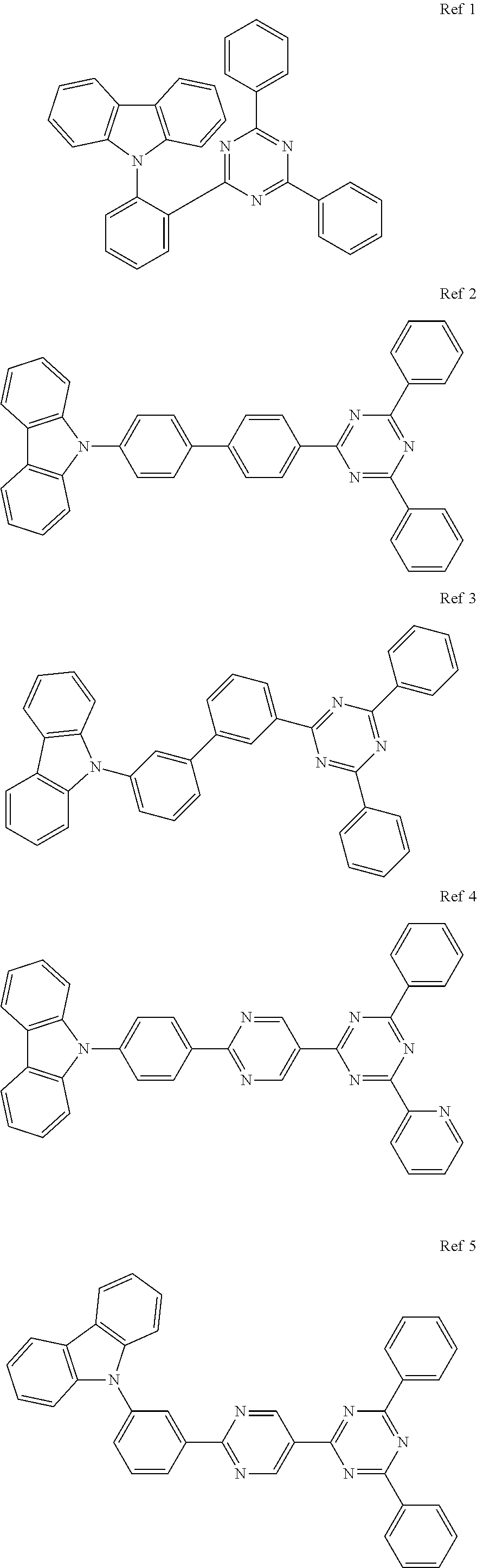
[0182] The compounds "Ref1" to "Ref9" were used instead of the compound "A" in Example 1 such that the OLEDs of Comparative Examples 1 to 9 were manufactured.
##STR00362## ##STR00363##
[0183] (4) Example 20 (Ex20)
[0184] A glass substrate (ITO substrate) coated with indium-tin-oxide (ITO) with a thickness of 150 nm was washed by distilled water. After washing by the distilled water, the ITO substrate was ultrasonically washed with a solvent such as isopropyl alcohol, acetone or methanol and dried. The ITO substrate was transferred into a plasma cleaner, and then the ITO substrate was cleaned for 5 minutes using oxygen plasma. The hole injection layer with a thickness of 60 nm was formed on the ITO substrate by spin-coating PEDOT:PSS. The hole transporting layer (TAPC, 20 nm) and the electron blocking layer (mCP, 0 nm) were sequentially formed on the hole injection layer by using the thermal evaporator. The emitting material layer (mCP (host), and the compound "A" (assist dopant, 20% doping) and BD01 (dopant, 5% doping), 25 nm) was formed on the electron blocking layer. The electron transporting layer (TPBi, 30 nm), the electron injection layer (LiF, lnm) and the cathode (Al, 100 nm) were sequentially formed on the emitting material layer. The laminating structure was encapsulated in the glove box such that the OLED was manufactured.
[0185] (5) Examples 21 to 24 (Ex21 to 24)
[0186] The compounds "B", "F", "G" and "H" were used instead of the compound "A" in Example 1 such that the OLEDs of Examples 21 to 24 were manufactured, respectively.
[0187] The electron and the hole were injected into the OLED by using the Keithley 2400 source measurement, and the luminance is measured using the Konica Minolta spectrophotometer (CS-2000). The performance of the OLED of Examples and Comparative Examples was measured under atmospheric pressure and listed in Table 2. (H: host, D1: assist dopant (first dopant), D2: dopant (second dopant), V: driving voltage [V], EQE: external quantum efficiency [%])
TABLE-US-00002 TABLE 2 EML CIE H D1 D2 V EQE Cd/A X y CE1 mCP -- Ref 1 6 9.3 14.6 0.15 0.22 CE2 mCP -- Ref 2 6 6.8 9.8 0.15 0.20 CE3 mCP -- Ref 3 6 8.5 13.8 0.15 0.20 CE4 mCP -- Ref 4 6 7.1 10.2 0.16 0.22 CE5 mCP -- Ref 5 6 9.1 14.3 0.16 0.23 CE6 mCP -- Ref 6 6 11 29.1 0.20 0.44 CE7 mCP Ref 7 6.1 12.2 18.7 0.22 0.25 CE8 mCP Ref 8 5.9 9.2 20.8 0.22 0.30 CE9 mCP Ref 9 5.8 10.8 22.1 0.22 0.33 Ex1 mCP -- A 5.5 14.2 30.9 0.15 0.20 Ex2 mCP -- B 5.4 14.7 31.3 0.15 0.20 Ex3 mCP -- C 5.5 15.3 31.6 0.15 0.20 Ex4 mCP -- D 5.6 14.8 30.3 0.15 0.20 Ex5 mCP -- E 5.4 13.9 30.1 0.15 0.20 Ex6 mCP -- F 5.5 14.9 30.5 0.15 0.20 Ex7 mCP -- G 5.5 15.1 31.5 0.15 0.20 Ex8 mCP -- H 5.6 14.3 30.9 0.15 0.20 Ex9 mCP -- I 5.5 14.3 30.7 0.15 0.20 Ex10 mCP -- J 5.5 14.8 31.2 0.15 0.20 Ex11 mCP -- K 5.6 15.2 31.8 0.15 0.20 Ex12 mCP -- L 5.6 15.1 31.5 0.15 0.22 Ex13 mCP -- M 5.6 15.7 31.9 0.15 0.22 Ex14 mCP -- N 5.7 15.3 31.8 0.15 0.22 Ex15 mCP -- O 5.6 14.8 31.3 0.15 0.22 Ex16 mCP -- P 5.6 14.9 31.5 0.15 0.22 Ex17 mCP -- Q 5.6 15.2 31.7 0.15 0.22 Ex18 mCP -- R 5.7 15.1 31.8 0.15 0.22 Ex19 mCP -- S 5.7 14.6 31.1 0.15 0.23 Ex20 mCP A BD01 5.5 16.8 44.2 0.14 0.11 Ex21 mCP B BD01 5.6 15.9 40.1 0.14 0.11 Ex22 mCP F BD01 5.6 16.5 42.3 0.14 0.12 Ex23 mCP G BD01 5.6 16.1 42.1 0.14 0.12 Ex24 mCP H BD01 5.5 15.8 41.5 0.14 0.12
[0188] As illustrated above, the emitting layer was formed using a thermally active delayed fluorescent compound, and the results of the performance evaluation are shown in Table 2. As shown in Table 2, all of the OLED of Examples using the compound of the present disclosure has the quantum efficiency over 5% (when the light extraction efficiency is 20%) which is the maximum external quantum efficiency that can be obtained from the general fluorescent device.
[0189] This shows that the compound of the present disclosure is capable of efficient transition of triplet energy to singlet energy through thermally active delayed fluorescence. In addition, the OLED of Examples using the compound of the present disclosure has a lower driving voltage and higher efficiency and EQE compared to Comparative Examples 1 to 9. Moreover, referring to Examples 20 to 24 using the compound of the present disclosure as the assist dopant, the OLED provides the dark blue emission and has excellent performance.
[0190] The compound of the present disclosure, which can solve the problem of the external quantum efficiency of the conventional fluorescent material, can be used as a TADF material as well as a fluorescent material. Since the electron donor unit and the electron acceptor unit co-exist in the molecule such that exciplex can be provided, the OLED using the compound of the present disclosure has properties of high efficiency, long lifespan and low driving voltage.
[0191] [OLED]
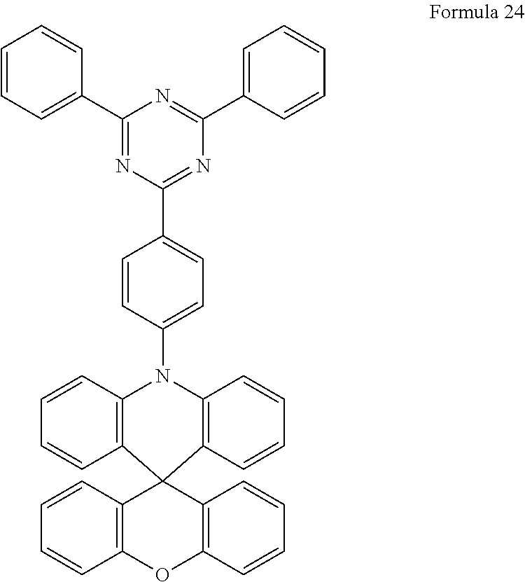
[0192] The hole injection layer (HATCN, 50 .ANG.), the hole transporting layer (NPB, 500 .ANG.), the electron blocking layer (MCP, 100 .ANG.), the emitting material layer (host and dopant (30 wt %), 250 .ANG.), the electron transporting layer (TPBi, 300 .ANG.), the electron injection layer (LiF, 10 .ANG.) and the cathode (Al, 1000 .ANG.) are sequentially formed on the ITO substrate to form the OLED. The compound in Formula 24 is used as the dopant.
##STR00364##
[0193] (1) Example 25 (Ex25)
[0194] The compound "A" is used as the host.
[0195] (2) Example 26 (Ex26)
[0196] The compound "I" is used as the host.
[0197] (3) Example 27 (Ex27)
[0198] The compound "Y" is used as the host.
[0199] (4) Comparative Example 10 (CE10)
[0200] The compound in Formula 25 is used as the host.
[0201] (5) Comparative Example 11 (CE11)
[0202] The compound "Ref9" is used as the host.
##STR00365##
[0203] Properties, i.e., driving voltage, external quantum efficiency (EQE), efficiency (cd/A) and color coordinate, of the OLED manufactured in Examples 25 to 27 and Comparative Examples 10 and 11 were measured using a current source (KEITHLEY) and a photometer (PR650) and listed in Table 3.
TABLE-US-00003 TABLE 3 voltage [V] EQE (%) cd/A CIE (x, y) CE10 5.4 8.1 15.1 (0.18, 0.37) CE11 4.2 9.6 17.5 (0.17, 0.36) EX25 3.8 16.9 35.0 (0.17, 0.34) Ex26 3.8 16.2 34.6 (0.17, 0.37) Ex27 3.7 16.2 32.6 (0.17, 0.35)
[0204] As shown in Table 3, when the compound of the present disclosure is used as a host of the emitting material layer, the driving voltage is reduced and the quantum efficiency and luminance are improved. Moreover, the compound of the present disclosure as the host has properties suitable for a delayed fluorescent dopant.
[0205] FIG. 3 is a schematic cross-sectional view of an OLED according to a second embodiment of the present disclosure.
[0206] As shown in FIG. 3, an OLED D includes the first electrode 160 and the second electrode 164, which face each other, and the organic emitting layer 162 therebetween. The organic emitting layer 162 includes an EML 340, which includes first and second layers 342 and 344 and is positioned between the first and second electrodes 160 and 164, an HTL 320 between the first electrode 160 and the EML 340 and an ETL 360 between the second electrode 164 and the EML 340.
[0207] In addition, the organic emitting layer 162 may further include a HIL 310 between the first electrode 160 and the HTL 320 and an EIL 370 between the second electrode 164 and the ETL 360.
[0208] Moreover, the organic emitting layer 162 may further include an EBL 330 between the HTL 320 and the EML 340 and a HBL 350 between the EML 340 and the ETL 360.
[0209] For example, in the EML 340, the first layer 342 (e.g., a first emitting material layer) may include the compound of the present disclosure as a first host and may further include a delayed fluorescent dopant (first dopant), and the second layer 344 (e.g., a second emitting material layer) may include a second host and a fluorescent dopant (second dopant). Alternatively, the second layer 344 may include the compound of the present disclosure as a first host and may further include a delayed fluorescent dopant (first dopant), and the first layer 342 may include a second host and a fluorescent dopant (second dopant). In this instance, the second host may be the compound of the present disclosure. The energy level of singlet state of the delayed fluorescent dopant is higher than that of the fluorescent dopant.
[0210] The OLED, where the first layer 342 includes the delayed fluorescent dopant and the second layer 344 includes the fluorescent dopant, will be explained.
[0211] In the OLED D, the energy level of singlet state and the energy level of triplet state of the delayed fluorescent dopant are transferred into the fluorescent dopant such that the light emission is provided from the fluorescent dopant. As a result, the quantum efficiency of the OLED D is increased, and the FWHM of the OLED D is narrowed.
[0212] The delayed fluorescent dopant has high quantum efficiency. However, since the light emitted from the delayed fluorescent dopant has wide FWHM, the light from the delayed fluorescent dopant has poor color purity. On the other hand, the fluorescence dopant has narrow FWHM and high color purity. However, since the energy level of triplet state of the fluorescence dopant is not involved in the emission, the fluorescence dopant has low quantum efficiency.
[0213] Since the EML 340 of the OLED D in the present disclosure includes the first layer 342, which includes the delayed fluorescent dopant, and the second layer 344, which includes the fluorescence dopant, the OLED D has advantages in both the emitting efficiency and the color purity.
[0214] The energy level of triplet state of the delayed fluorescent dopant is converted into the energy level of singlet state of the delayed fluorescent dopant by the reverse intersystem crossing (RISC) effect, and the energy level of singlet state of the delayed fluorescent dopant is transferred into the energy level of singlet state of the fluorescence dopant. Namely, the difference between the energy level of triplet state of the delayed fluorescent dopant and the energy level of singlet state of the delayed fluorescent dopant is not greater than 0.3 eV such that the energy level of triplet state of the delayed fluorescent dopant is converted into the energy level of singlet state of the delayed fluorescent dopant by the RISC effect.
[0215] As a result, the delayed fluorescent dopant has an energy transfer function, and the first layer 342 including the delayed fluorescent dopant is not engaged in the light emission. The light emission is generated in the second layer 344 including the fluorescence dopant.
[0216] The energy level of triplet state of the delayed fluorescent dopant is converted into the energy level of singlet state of the delayed fluorescent dopant by the RISC effect. In addition, since the energy level of singlet state of the delayed fluorescent dopant is higher than that of the fluorescence dopant, the energy level of singlet state of the delayed fluorescent dopant is transferred into the energy level of singlet state of the fluorescence dopant. As a result, the fluorescence dopant emits the light using the energy level of singlet state and the energy level of triplet state such that the quantum efficiency (emitting efficiency) of the OLED D is improved.
[0217] In other words, the OLED D and the organic light emitting display device 100 (of FIG. 1) including the OLED D has advantages in both the emitting efficiency (quantum efficiency) and the color purity (FWHM).
[0218] In each of the first and second layers 342 and 344, the first and second hosts may have a percentage by weight being larger than the delayed fluorescent dopant and the fluorescence dopant, respectively. In addition, the percentage by weight of the delayed fluorescent dopant in the first layer 342 may be greater than that of the fluorescence dopant in the second layer 344. As a result, the energy transfer from the delayed fluorescent dopant into the fluorescence dopant is sufficiently generated.
[0219] The energy level of singlet state of the first host is greater than that of the delayed fluorescent dopant, and the energy level of triplet state of the first host is greater than that of the delayed fluorescent dopant. In addition, the energy level of singlet state of the second host is greater than that of the fluorescence dopant.
[0220] When not satisfying this condition, a quenching happens at the first and second dopants or an energy transfer from the host to the dopant does not happen, and thus the quantum efficiency of the OLED D is reduced.
[0221] As mentioned above, the compound of the present disclosure has high energy level of triplet state, the energy transfer efficiency to the delayed fluorescent dopant is increased such that the quantum efficiency of the OLED D is improved.
[0222] For example, the second host, which is included in the second layer 344 with the fluorescence dopant, may be same as a material of the HBL 350. In this instance, the second layer 344 may have a hole blocking function with an emission function. Namely, the second layer 344 may serve as a buffer layer for blocking the hole. When the HBL 350 is omitted, the second layer 344 serves as an emitting material layer and a hole blocking layer.
[0223] When the first layer 342 includes the fluorescence dopant and the second layer 344 includes the delayed fluorescent dopant, the first host of the first layer 342 may be same as a material of the EBL 330. In this instance, the first layer 342 may have an electron blocking function with an emission function. Namely, the first layer 342 may serve as a buffer layer for blocking the electron. When the EBL 330 is omitted, the first layer 342 serves as an emitting material layer and an electron blocking layer.
[0224] On the other hand, the compound of the present disclosure may have a delayed fluorescent property to use as a delayed fluorescent dopant. In this instance, one of the first and second layers 342 and 344 of the EML 340 may include the compound of the present disclosure as a first dopant (delayed fluorescent dopant), and the other one of the first and second layers 342 and 344 may include a fluorescent dopant or a phosphorescent dopant as a second dopant.
[0225] FIG. 4 is a schematic cross-sectional view of an OLED according to a third embodiment of the present disclosure.
[0226] As shown in FIG. 4, an OLED D includes the first and second electrodes 160 and 164, which face each other, and the organic emitting layer 162 therebetween. The organic emitting layer 162 includes an EML 440, which includes first to third layers 442, 444, and 446 and is positioned between the first and second electrodes 160 and 164, a HTL 420 between the first electrode 160 and the EML 440 and an ETL 460 between the second electrode 164 and the EML 440.
[0227] In addition, the organic emitting layer 162 may further include a HIL 410 between the first electrode 160 and the HTL 420 and an EIL 470 between the second electrode 164 and the ETL 460.
[0228] Moreover, the organic emitting layer 162 may further include an EBL 430 between the HTL 420 and the EML 440 and a HBL 450 between the EML 440 and the ETL 460.
[0229] In the EML 440, the first layer 442 is positioned between the second layer 444 and the third layer 446. Namely, the second layer 444 is positioned between the EBL 430 and the first layer 442, and the third layer 446 is positioned between the first layer 442 and the HBL 450.
[0230] The first layer 442 (e.g., a first emitting material layer) includes the compound of the present disclosure as a first host and further includes a delayed fluorescent dopant (first dopant). The second layer 444 includes a second host and a fluorescent dopant (second dopant), and the third layer 446 includes a third host and a fluorescent dopant (third dopant). The fluorescent dopants in the second and third layers 444 and 446 may be same or different. In addition, the second host and the third host may be the compound of the present disclosure. The delayed fluorescent dopant has an energy level of singlet state being larger than the fluorescent dopant.
[0231] In the OLED D, the energy level of singlet state and the energy level of triplet state of the delayed fluorescent dopant in the first layer 442 are transferred into the fluorescence dopant in the second layer 444 and/or the third layer 446 such that the emission is generated from the fluorescence dopant. As a result, the quantum efficiency of the OLED D is increased, and the FWHM of the OLED D is narrowed.
[0232] In each of the first to third layers 442, 444 and 446, the first to third hosts may have a percentage by weight being larger than the delayed fluorescent dopant and the fluorescence dopant, respectively. In addition, the percentage by weight of the delayed fluorescent dopant (i.e., the first dopant) in the first layer 442 may be greater than that of each of the fluorescence dopant (i.e., the second dopant) in the second layer 444 and the fluorescence dopant (i.e., the third dopant) in the third layer 446.
[0233] The energy level of singlet state of the first host is greater than that of the delayed fluorescent dopant, and the energy level of triplet state of the first host is greater than that of the delayed fluorescent dopant. In addition, the energy level of singlet state of the second host is greater than that of the fluorescent dopant in the second layer 444, and the energy level of singlet state of the third host is greater than that of the fluorescent dopant in the third layer 446.
[0234] As mentioned above, the compound of the present disclosure has high energy level of triplet state, the energy transfer efficiency to the delayed fluorescent dopant is increased such that the quantum efficiency of the OLED D is improved.
[0235] For example, the second host in the second layer 444 may be same as a material of the EBL 430. In this instance, the second layer 444 may have an electron blocking function with an emission function. Namely, the second layer 444 may serve as a buffer layer for blocking the electron. When the EBL 430 is omitted, the second layer 444 serves as an emitting material layer and an electron blocking layer.
[0236] The third host in the third layer 446 may be same as a material of the HBL 450. In this instance, the third layer 446 may have a hole blocking function with an emission function. Namely, the third layer 446 may serve as a buffer layer for blocking the hole. When the HBL 450 is omitted, the third layer 446 serves as an emitting material layer and a hole blocking layer.
[0237] The second host in the second layer 444 may be same as a material of the EBL 430, and the third host in the third layer 446 may be same as a material of the HBL 450. In this instance, the second layer 444 may have an electron blocking function with an emission function, and the third layer 446 may have a hole blocking function with an emission function. Namely, the second layer 444 may serve as a buffer layer for blocking the electron, and the third layer 446 may serve as a buffer layer for blocking the hole. When the EBL 430 and the HBL 450 are omitted, the second layer 444 serves as an emitting material layer and an electron blocking layer and the third layer 446 serves as an emitting material layer and a hole blocking layer.
[0238] On the other hand, the compound of the present disclosure may have a delayed fluorescent property to use as a delayed fluorescent dopant. In this instance, the first layer 442 of the EML 440 may include the compound of the present disclosure as a first dopant (delayed fluorescent dopant), and each of the second and third layers 444 and 446 may include a fluorescent dopant or a phosphorescent dopant.
[0239] It will be apparent to those skilled in the art that various modifications and variations can be made in the present disclosure without departing from the spirit or scope of the present disclosure. Thus, it is intended that the present disclosure cover the modifications and variations of the present disclosure provided they come within the scope of the appended claims and their equivalents.
* * * * *


D00000
D00001

D00002

XML
uspto.report is an independent third-party trademark research tool that is not affiliated, endorsed, or sponsored by the United States Patent and Trademark Office (USPTO) or any other governmental organization. The information provided by uspto.report is based on publicly available data at the time of writing and is intended for informational purposes only.
While we strive to provide accurate and up-to-date information, we do not guarantee the accuracy, completeness, reliability, or suitability of the information displayed on this site. The use of this site is at your own risk. Any reliance you place on such information is therefore strictly at your own risk.
All official trademark data, including owner information, should be verified by visiting the official USPTO website at www.uspto.gov. This site is not intended to replace professional legal advice and should not be used as a substitute for consulting with a legal professional who is knowledgeable about trademark law.