Cable Assembly
LITTLE; TERRANCE F.
U.S. patent application number 16/701067 was filed with the patent office on 2020-06-04 for cable assembly. The applicant listed for this patent is FOXCONN (KUNSHAN) COMPUTER CONNECTOR CO., LTD. FOXCONN INTERCONNECT TECHNOLOGY LIMITED. Invention is credited to TERRANCE F. LITTLE.
| Application Number | 20200176923 16/701067 |
| Document ID | / |
| Family ID | 70850672 |
| Filed Date | 2020-06-04 |


View All Diagrams
| United States Patent Application | 20200176923 |
| Kind Code | A1 |
| LITTLE; TERRANCE F. | June 4, 2020 |
CABLE ASSEMBLY
Abstract
A cable includes an electrical connector at one end and a sensor at the other end. The connector includes a terminal module having a plurality of contacts embedded within an insulator wherein each contact has a resilient contacting section exposed upon to an exterior in a first vertical direction, and a soldering section exposed in a second vertical direction to be connected to the corresponding wires of the cable and selectively further to a resistor. The sensor includes a case enclosing an LED (Light Emitting Diode) and a PD (Photo Diode both of which are respectively connected to the corresponding contacts respectively soldered to the corresponding wires.
| Inventors: | LITTLE; TERRANCE F.; (Fullerton, CA) | ||||||||||
| Applicant: |
|
||||||||||
|---|---|---|---|---|---|---|---|---|---|---|---|
| Family ID: | 70850672 | ||||||||||
| Appl. No.: | 16/701067 | ||||||||||
| Filed: | December 2, 2019 |
Related U.S. Patent Documents
| Application Number | Filing Date | Patent Number | ||
|---|---|---|---|---|
| 62773197 | Nov 30, 2018 | |||
| 62899156 | Sep 12, 2019 | |||
| Current U.S. Class: | 1/1 |
| Current CPC Class: | A61B 5/6847 20130101; H01R 4/023 20130101; H01R 13/5224 20130101; H01R 2201/12 20130101; H01R 13/5825 20130101; A61B 2562/227 20130101; H01R 13/2464 20130101; H01R 13/5216 20130101; H01R 13/6616 20130101; H01R 13/405 20130101 |
| International Class: | H01R 13/52 20060101 H01R013/52; A61B 5/00 20060101 A61B005/00 |
Claims
1. A cable assembly comprising: a cable including a plurality of wires therein and defining thereof opposite ends with an electrical connector secured to one end and a sensor sub-assembly secure to the other end; the connector including a terminal module including a plurality of contacts integrally formed with an insulative housing via an insert-molding process, a plurality of passageways formed in an upper face of the housing, each passageway extending in a front-to-back direction, each of said contacts including a downward facing rear soldering section mechanically and electrically connected to the corresponding wires, respectively, an upward facing upper contacting section extending above the corresponding groove in a vertical direction perpendicular to said front-to-back direction, and a curved middle section linked between the contacting section and the soldering section and deflectable in the vertical direction; wherein the curved middle section is formed after the contact is molded with the insulative housing.
2. The cable assembly as claimed in claim 1, wherein a transverse slot extends across said passageways in a transverse direction perpendicular to both the front-to-back direction and the vertical direction.
3. The cable assembly as claimed in claim 1, further including a resistor soldered upon the soldering sections of the corresponding two contacts.
4. The cable assembly as claimed in claim 1, further including a glue block covering the soldering sections, the wires and the resistor.
5. The cable assembly as claimed in claim 4, wherein said housing forms a cavity to receive said glue block therein.
6. The cable assembly as claimed in claim 1, wherein the curved middle section defines a U-shaped configuration located within the corresponding passageway.
7. The cable assembly as claimed in claim 6, wherein said U-shaped configuration include an upper arm, a lower arm and a bight therebetween, and the lower arm abuts against an upward surface of the corresponding passageway.
8. The cable assembly as claimed in claim 1, wherein the passageways extend forwardly through the housing in the front-to-back direction.
9. The cable assembly as claimed in claim 1, wherein the sensor sub-assembly includes an overmolding housing forming an LED (Light Emitting Diode) cavity receiving an LED and a PD (Photo Diode) cavity receiving a PD therein, and the housing forms a transverse receiving slot communicating with both the LED cavity and the PD cavity.
10. The cable assembly as claimed in claim 9, wherein an LED lens cover is received within the LED cavity atop of the LED, and a PD lens cover is received within the PD cavity atop the PD.
11. A cable connector assembly comprising: a contact module including a plurality of contacts integrally formed within an insulator via an insert-molding process, each of said contacts including a horizontal section extending along a front-to-back direction with two opposite top and bottom sides exposed to an exterior, a resilient curved contacting section spaced from the horizontal section in a vertical direction perpendicular to the front-to-back direction, and a bight linked therebetween; and a cable located behind the contact module and including a plurality of wires mechanically and electrically connected to the bottom sides of the horizontal sections of the corresponding contacts; wherein in each contact, a lance is stamped out of the horizontal section to form a corresponding opening, and said lance is embedded within the insulator and the opening is filled with material of the insulator.
12. The cable connector assembly as claimed in claim 11, wherein the insulator further includes a crossbar downwardly extending in a transverse direction perpendicular to both the front-to-back direction and the vertical direction, and pressing the upper side of the horizontal section.
13. The cable connector assembly as claimed in claim 12, wherein the upper cover forms a transverse bar downwardly pressing the crossbar of the insulator in the vertical direction.
14. The cable connector assembly as claimed in claim 11, further including an upper cover and a lower cover commonly sandwiching the contact module between in the vertical direction, wherein the contact module forms a mating port exposed to the exterior both forwardly in the front-to-back direction and upwardly in the vertical direction.
15. The cable connector assembly as claimed in claim 14, wherein the upper cover forms a front flange and the contact includes a tab at a free end of the contacting section pressed downwardly by the flange in a preloaded manner when the connector assembly is not mated.
16. The cable connector assembly as claimed in claim 15, wherein the tab is downwardly pressed to contact the top side of the horizontal section of the corresponding contact when the connector assembly is mated.
17. The cable connector assembly as claimed in claim 14, wherein the upper cover forms step structure downwardly pressing the insulator of the contact module.
18. The cable connector assembly as claimed in claim 17, wherein an upward structure is formed on an interior surface of the lower cover to upwardly press the insulator of the contact module so as to cooperate with the step structure of the upper cover to commonly sandwich the insulator of the contact module therebetween in the vertical direction.
19. The cable connector assembly as claimed in claim 14, wherein the insulator forms a vertical center wall, and the upper cover forms a pair of vertical side walls located by two sides of and having a similar configuration of the middle wall so as to form two contacting areas.
20. A cable assembly comprising: a cable including a plurality of wires therein and defining thereof opposite ends with an electrical connector secured to one end and a sensor sub-assembly secure to the other end; the connector including a terminal module including a plurality of contacts integrally formed with an insulative housing via an insert-molding process, a plurality of passageways formed in an upper face of the housing, each passageway extending in a front-to-back direction, each of said contacts including a rear soldering section mechanically and electrically connected to the corresponding wires, respectively, an upward facing upper contacting section extending above the corresponding groove in a vertical direction perpendicular to said front-to-back direction, and a curved middle section linked between the contacting section and the soldering section and deflectable in the vertical direction; wherein a transverse groove extends across the passageways in a transverse direction perpendicular to both the front-to-back direction and the vertical direction.
Description
BACKGROUND OF THE DISCLOSURE
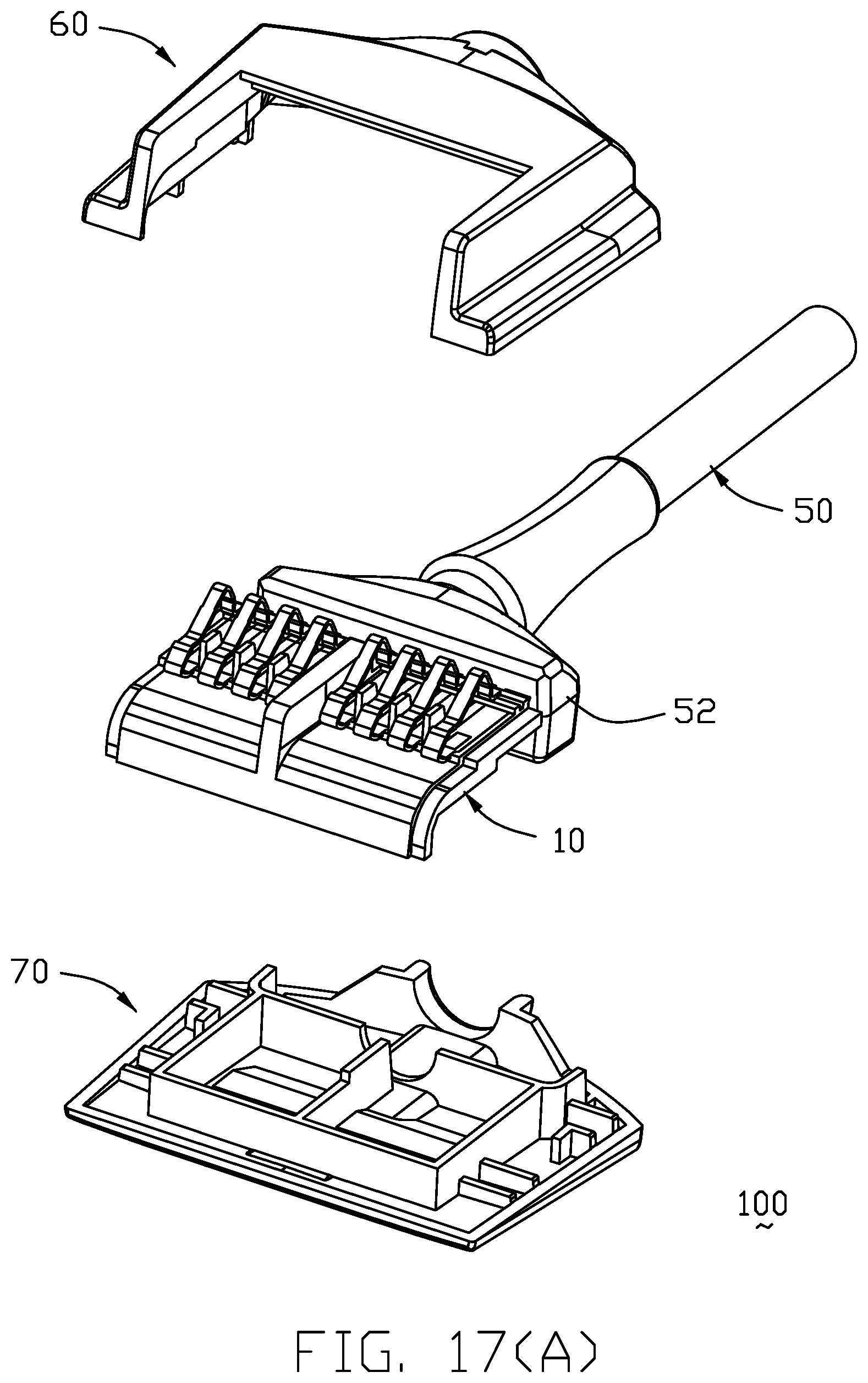
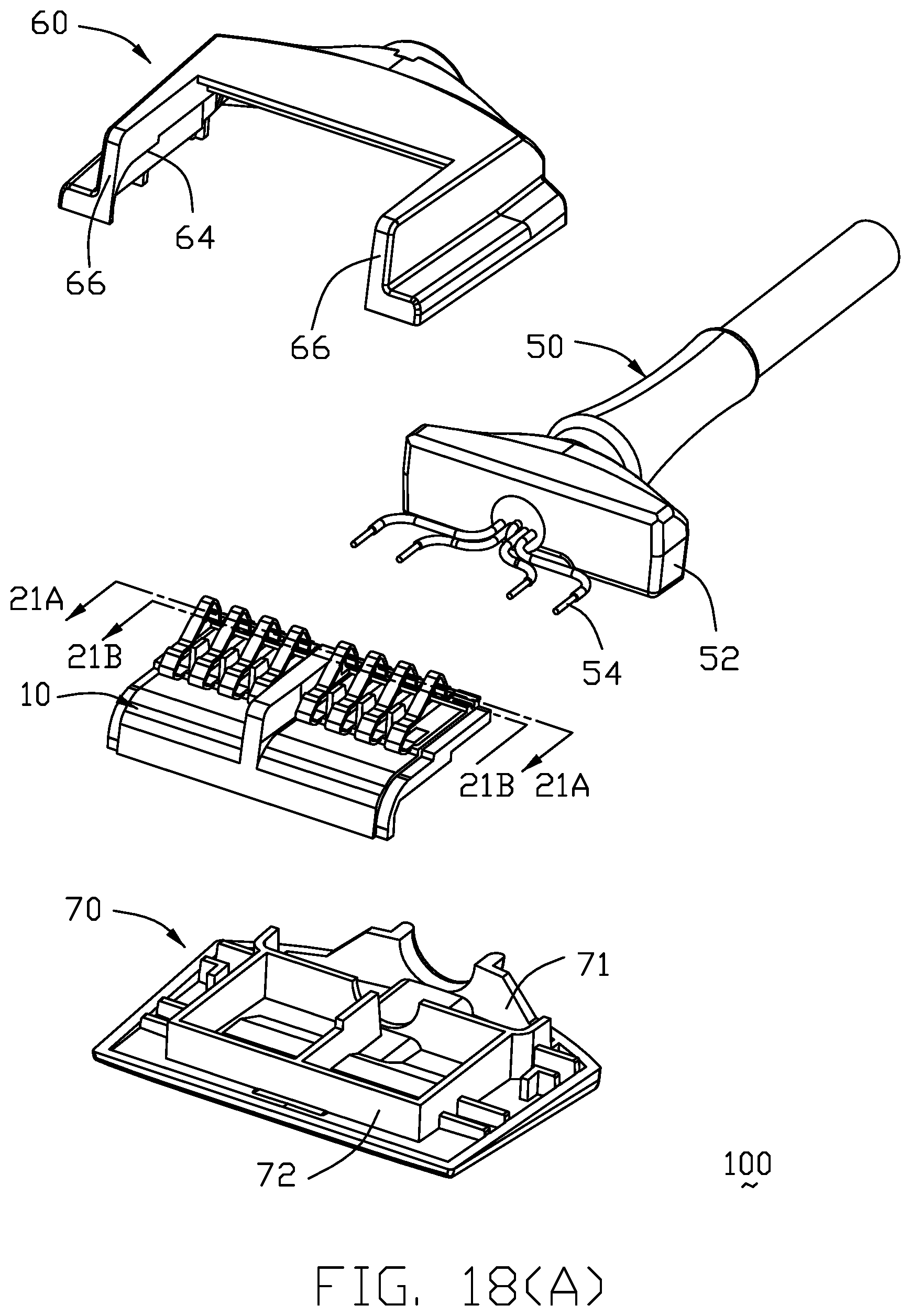
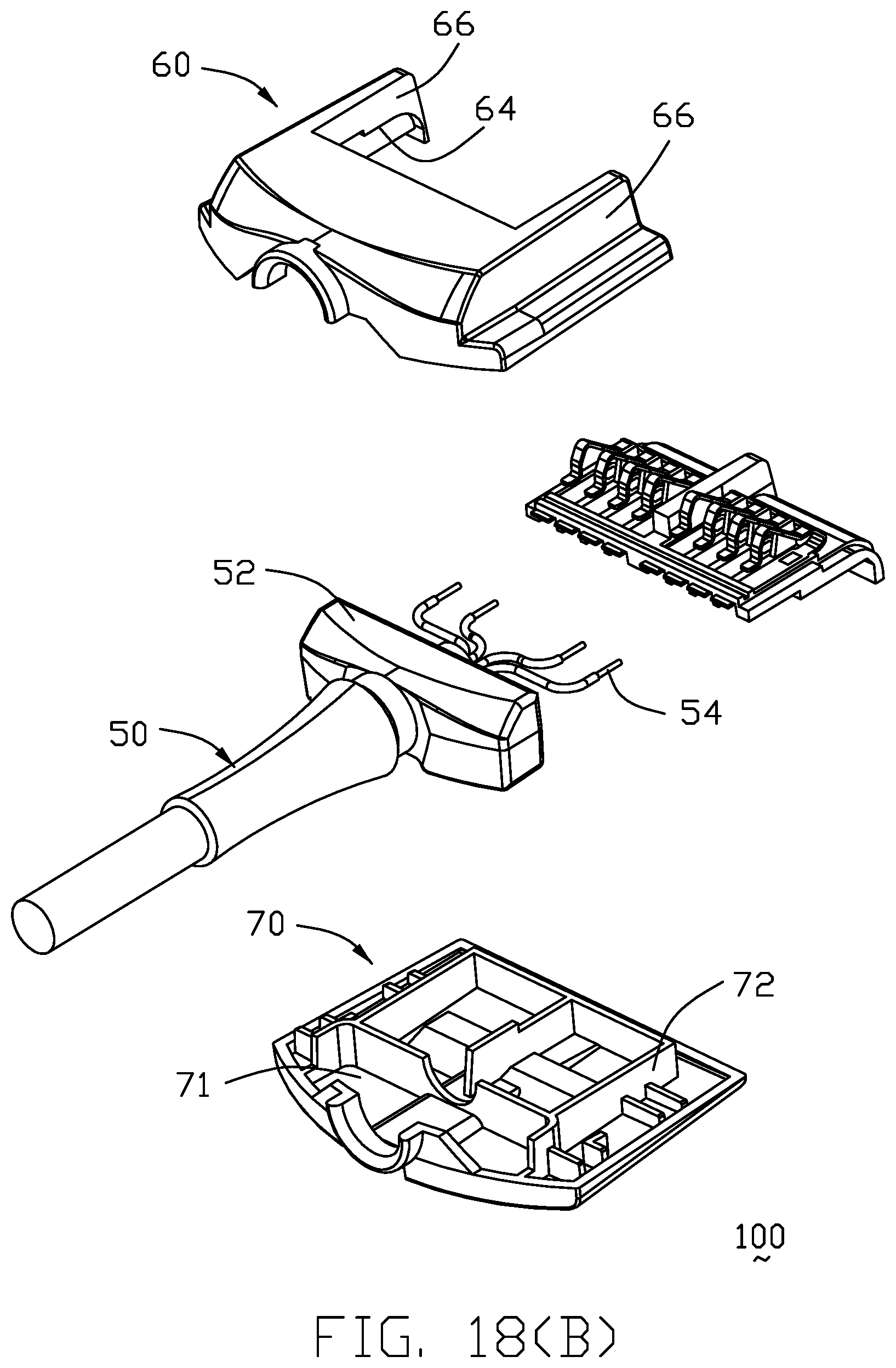
1. Field of the Disclosure
[0001] The present disclosure relates to a cable assembly, and more particularly to the cable assembly with superior waterproof and low cost.
2. Description of Related Arts
[0002] U.S. Pat. Nos. 9,439,574, 9,685,744, 9,698,545 and 9,722,375 disclose the medical device and the associated cables which may be used with the human body as shown in U.S. Pat. No. 8,527,038. Although the medical device is structured to be waterproofed, the conventional coupling cable connector of the cable assembly is constructed with relatively inferior waterproofing function. In addition, the traditional coupling connector requires to use a printed circuit board with a resistor mounted thereon, and the FPC used on the SPO2 (Saturation of Peripheral Oxygen) side, thus increasing the cost
[0003] An improved low cost cable assembly is desired.
SUMMARY OF THE DISCLOSURE
[0004] An object of the invention is to provide a cable assembly with superior waterproofing and low cost.
[0005] To achieve the above object, a cable assembly includes a cable with an electrical connector at one end and a sensor at the other end. The connector includes a terminal module having a plurality of contacts embedded within an insulator wherein each contact has a resilient contacting section exposed upon to an exterior in a first vertical direction, and a soldering section exposed in a second vertical direction to be connected to the corresponding wires of the cable and selectively further to a resistor. The sensor includes a case enclosing an LED (Light Emitting Diode) and a PD (Photo Diode both of which are respectively connected to the corresponding contacts respectively soldered to the corresponding wires.
[0006] Other objects, advantages and novel features of the disclosure will become more apparent from the following detailed description when taken in conjunction with the accompanying drawings.
BRIEF DESCRIPTION OF THE DRAWINGS
[0007] FIG. 1(A) is a perspective view of a cable assembly according to a first embodiment of the invention;
[0008] FIG. 1(B) is another perspective view of the cable assembly of FIG. 1(A);
[0009] FIG. 2(A) is a perspective view of the connector of the cable assembly of FIG. 1(A);
[0010] FIG. 2(B) is another perspective view of the electrical connector of the cable assembly of FIG. 2(A);
[0011] FIG. 3 is a perspective view of the electrical connector of the cable assembly of FIG. 2(A) wherein the contacts have not been bent to their final positions;
[0012] FIG. 4(A) is an exploded perspective view of the electrical connector of the cable assembly of FIG. 2(A);
[0013] FIG. 4(B) is another exploded perspective view of the electrical connector of the cable assembly of FIG. 4(A);
[0014] FIG. 5 is a plurality of contacts linked on a contact carrier of the electrical connector of the cable assembly of FIG. 3 wherein the contacts have not been bent to their final positions;
[0015] FIG. 6 is a perspective view of a partially assembled electrical connector of the cable assembly of FIG. 2(A);
[0016] FIG. 7 is a perspective view of a further partially assembled electrical connector of the cable assembly of FIG. 6;
[0017] FIG. 8 is a perspective view of a further partially assembled electrical connector of the cable assembly of FIG. 7;
[0018] FIG. 9 is an exploded perspective view of the electrical connector of the cable assembly of FIG. 2(A);
[0019] FIG. 10(A) is a cross-sectional view of the electrical connector of the cable assembly of FIG. 3;
[0020] FIG. 10(B) is a cross-sectional view of the electrical connector of the cable assembly of FIG. 2(A);
[0021] FIG. 10(C) is a cross-sectional view of a partially assembled electrical connector of FIG. 3;
[0022] FIG. 11 is a perspective view of the partially assembled electrical connector of FIG. 10(C);
[0023] FIG. 12(A) is a perspective view of the sensor sub-assembly of the cable assembly of FIG. 1(A);
[0024] FIG. 18 is a top view of the electrical connector of FIG. 12;
[0025] FIG. 12(B) is another perspective view of the sensor sub-assembly of the cable assembly of FIG. 1(A);
[0026] FIG. 13(A) is an exploded perspective view of the sensor sub-assembly of the cable assembly of FIG. 12(A);
[0027] FIG. 13(B) is another exploded perspective view of the sensor sub-assembly of the cable assembly of FIG. 13(A);
[0028] FIG. 14(A) is a further exploded perspective view of the sensor sub-assembly of the cable assembly of FIG. 13(A);
[0029] FIG. 14(B) is another further exploded perspective view of the sensor sub-assembly of the cable assembly of FIG. 14(A);
[0030] FIG. 15(A) is a cross-sectional view of the sensor sub-assembly of the cable assembly of FIG. 1(A);
[0031] FIG. 15(B) is a cross-sectional view of the sensor sub-assembly of the cable assembly of FIG. 1(A);
[0032] FIG. 15(C) is a cross-sectional view of the sensor sub-assembly of the cable assembly of FIG. 1(A); and
[0033] FIG. 16(A) is a perspective view of the cable connector assembly according to a second embodiment of the invention;
[0034] FIG. 16(B) is another perspective view of the cable connector assembly of FIG. 16(A);
[0035] FIG. 17(A) is an exploded perspective view of the cable connector assembly of FIG. 16(A);
[0036] FIG. 17(B) is another exploded perspective view of the cable connector assembly of FIG. 17(A);
[0037] FIG. 18(A) is a further exploded view of the cable connector assembly of FIG. 17(A);
[0038] FIG. 18(B) is another exploded perspective view of the cable connector assembly of FIG. 18(A)
[0039] FIG. 18(C) is another exploded perspective view of the cable connector assembly of FIG. 18(A);
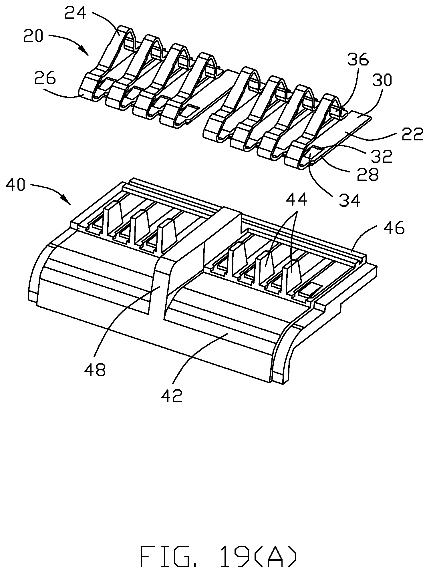
[0040] FIG. 19(A) is an exploded view of the contact module of the cable connector assembly of FIG. 18(A);
[0041] FIG. 19(B) is another exploded perspective view of the cable connector assembly of FIG. 19(A);
[0042] FIG. 20(A) is a cross-sectional view of the cable connector assembly of FIG. 16(A) along line 20-20;
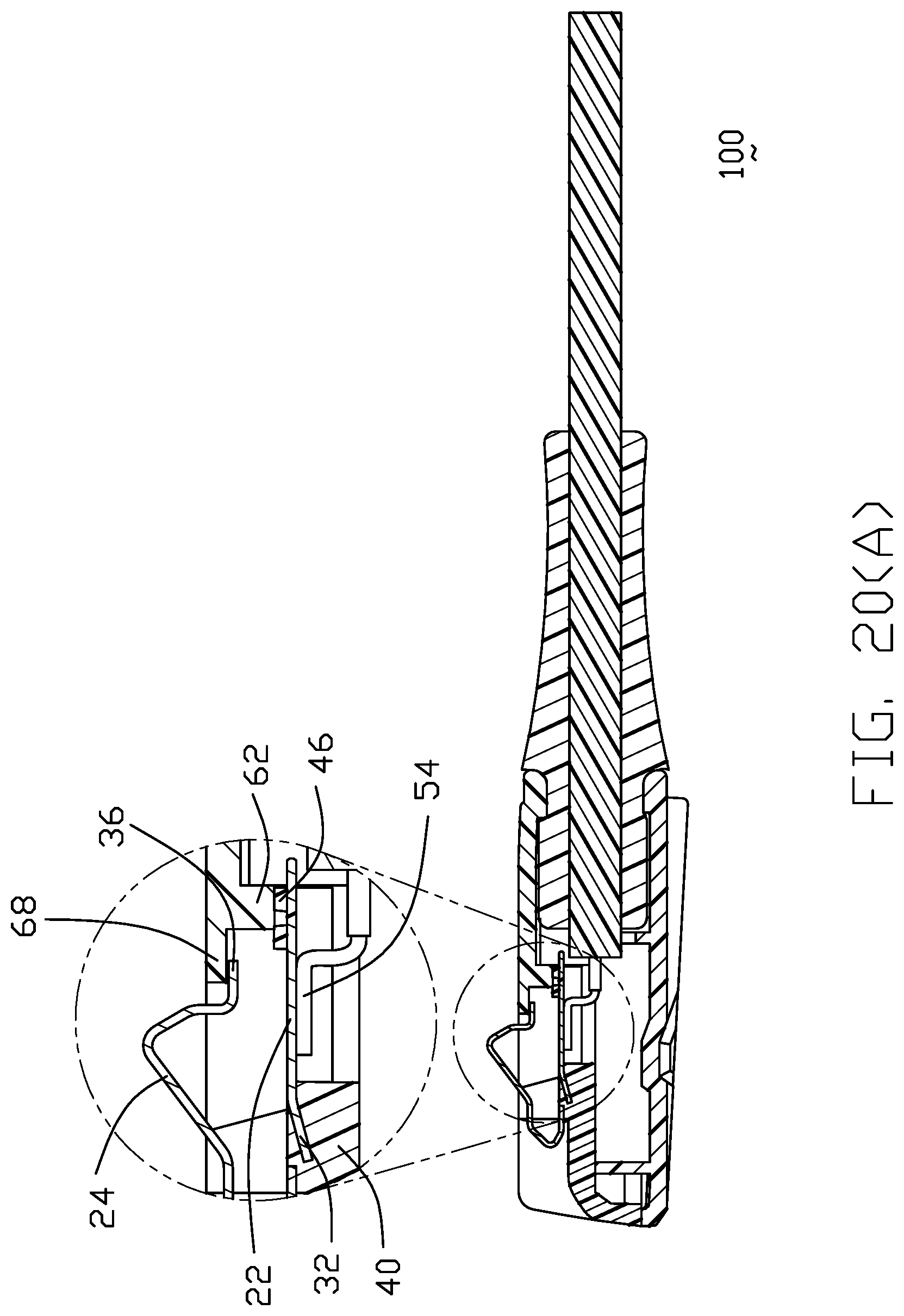
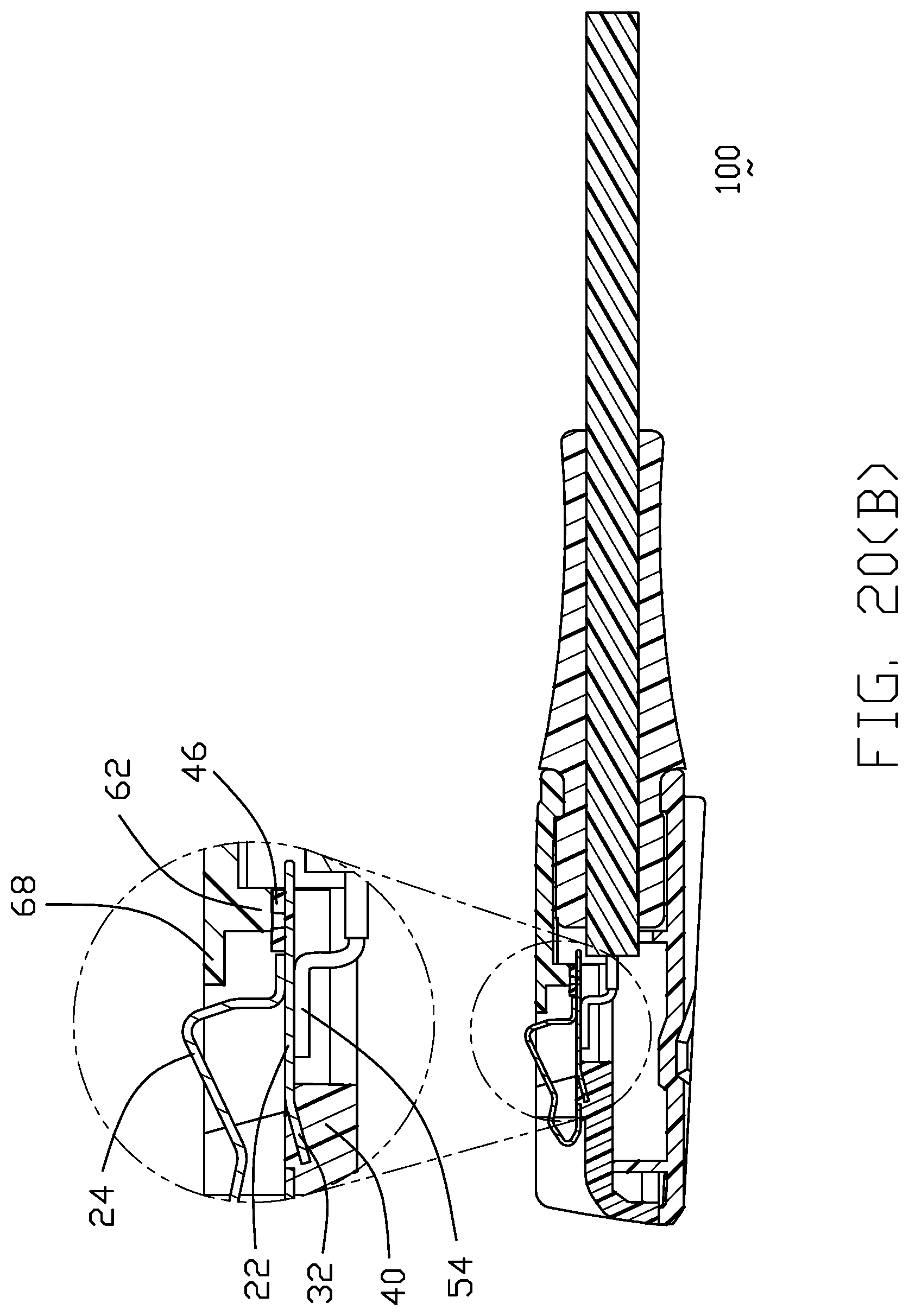
[0043] FIG. 20(B) is a cross-sectional view of the cable connector assembly of FIG. 20(A) wherein the contact is deflected during mating;
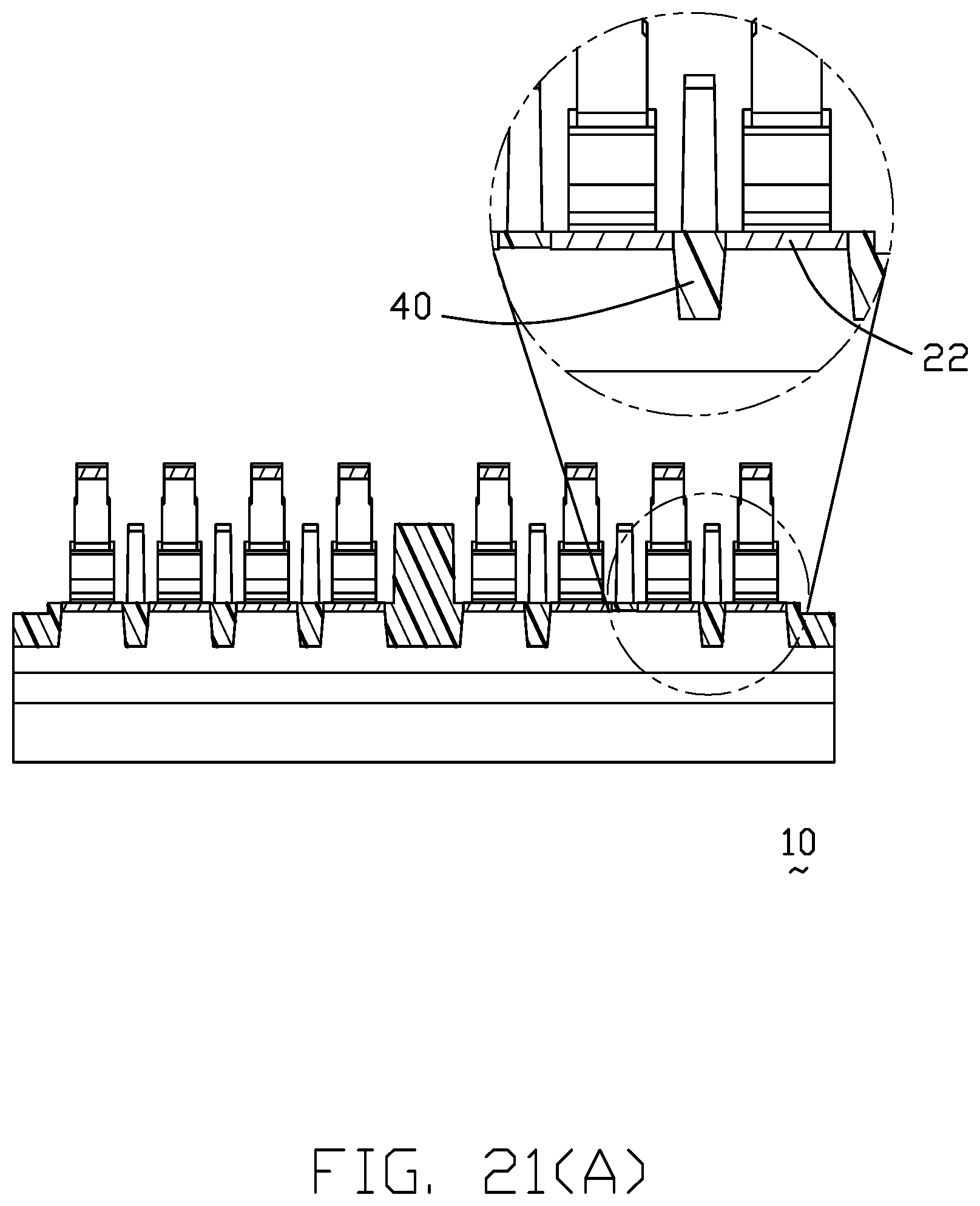
[0044] FIG. 21(A) is a cross-sectional view of the cable connector assembly of FIG. 1(A) along line 21A-21A;
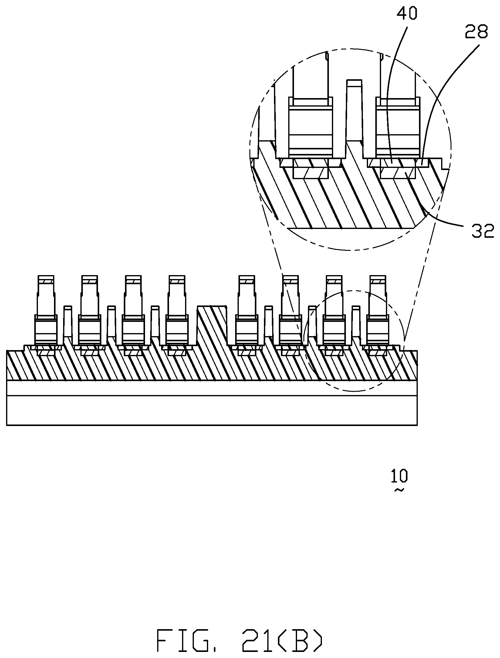
[0045] FIG. 21(B) is a cross-sectional view of the cable connector assembly of FIG. 1(A) along line 21B-21B; and
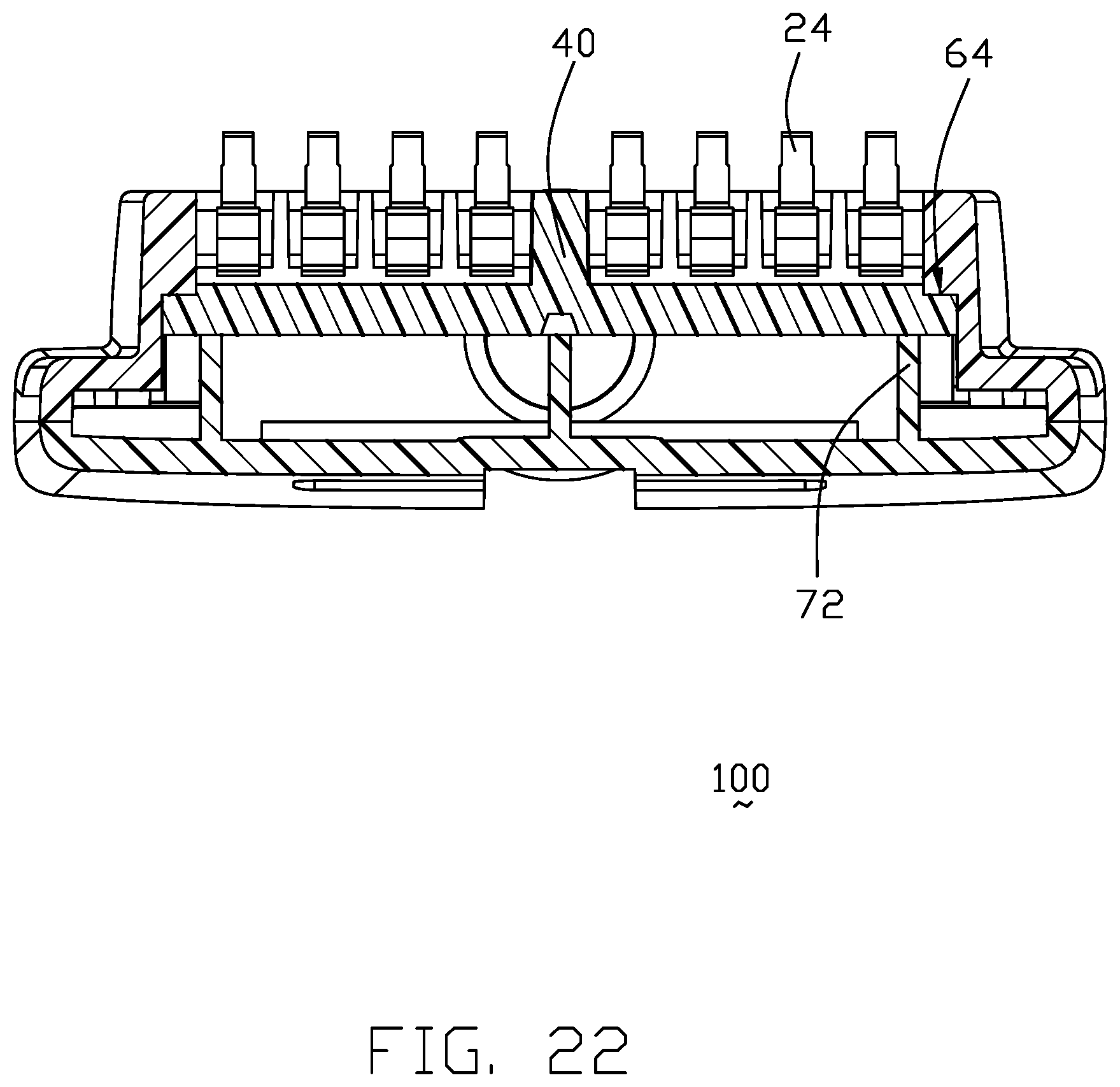
[0046] FIG. 22 is a cross-sectional view of the cable connector assembly of FIG. 1(A) along line 22-22.
DETAILED DESCRIPTION OF THE PREFERRED EMBODIMENT
[0047] Reference numerals are used to describe in detail to only the referred embodiment of the present disclosure.
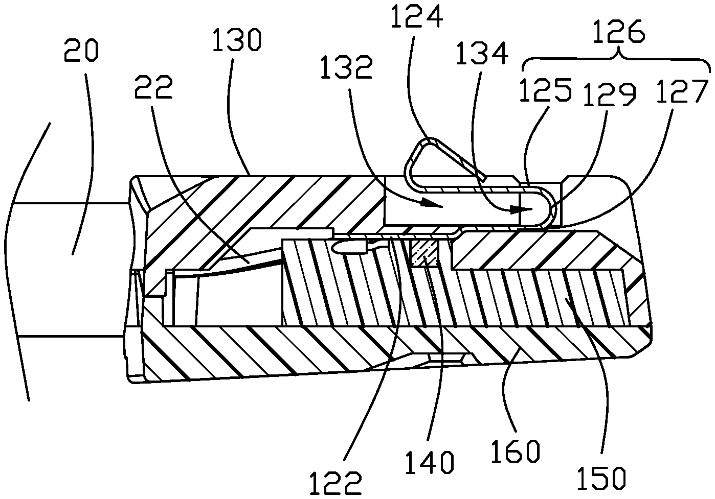
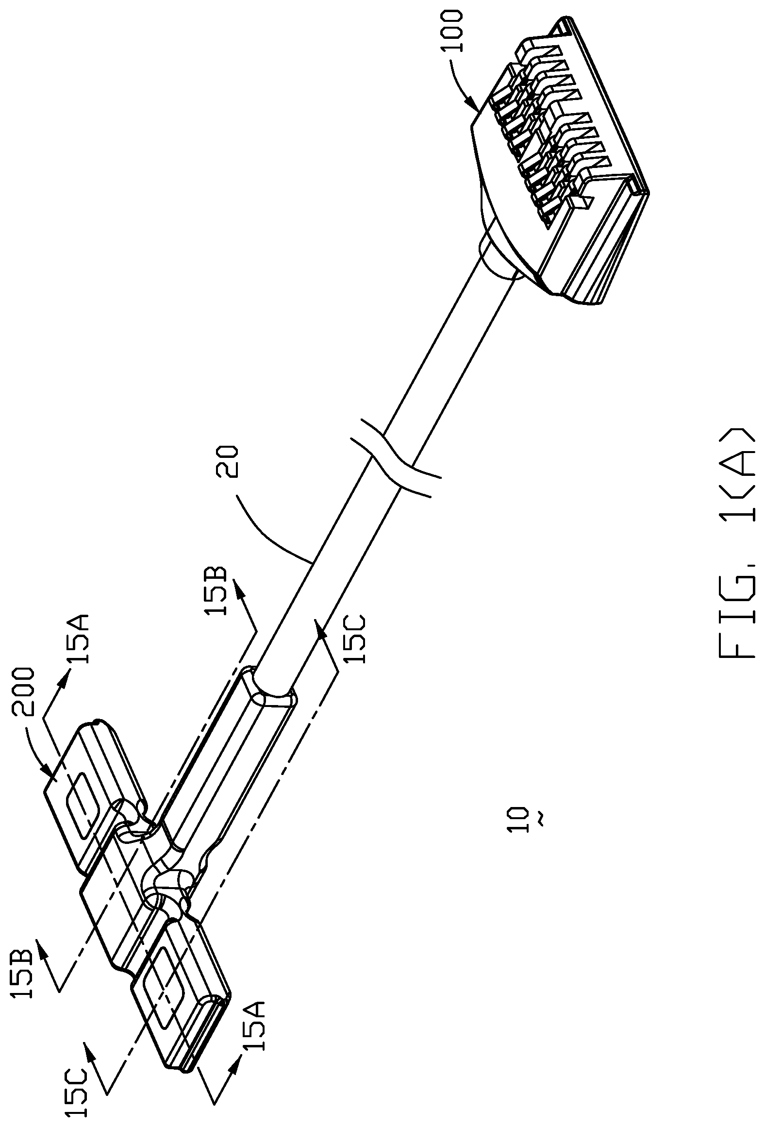
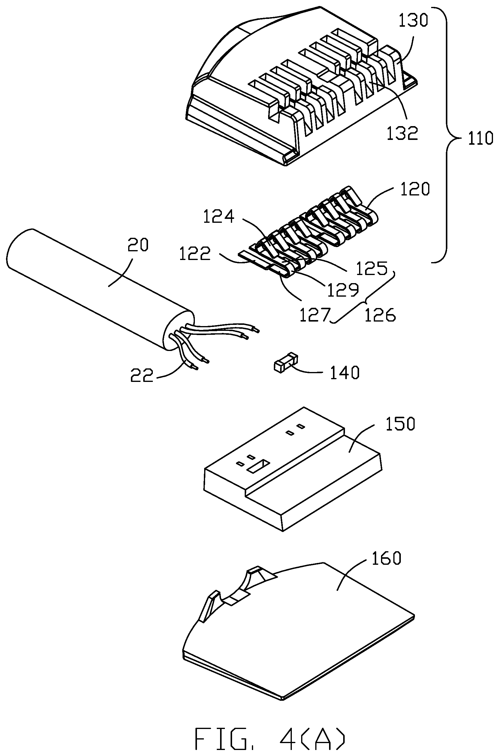
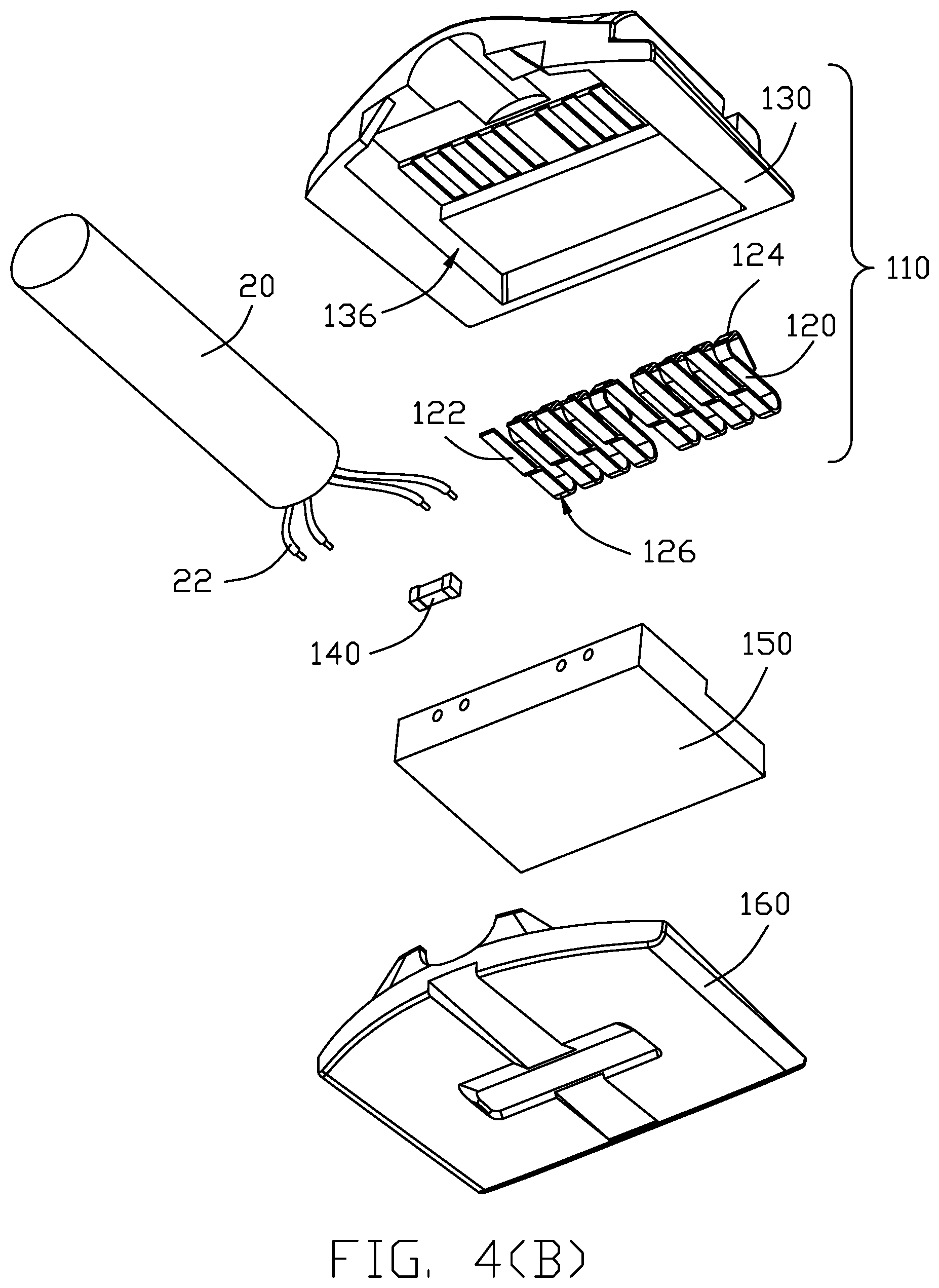
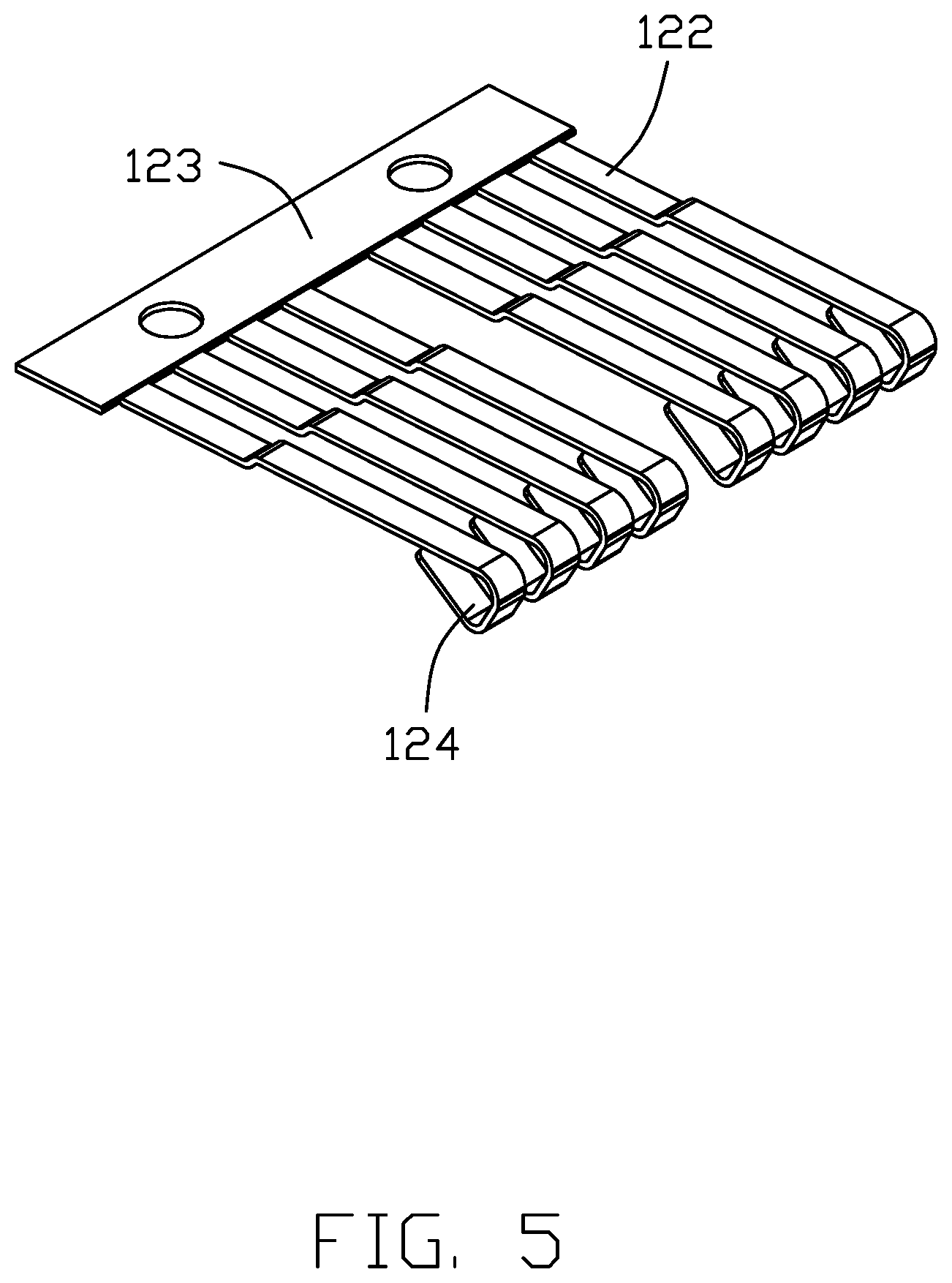
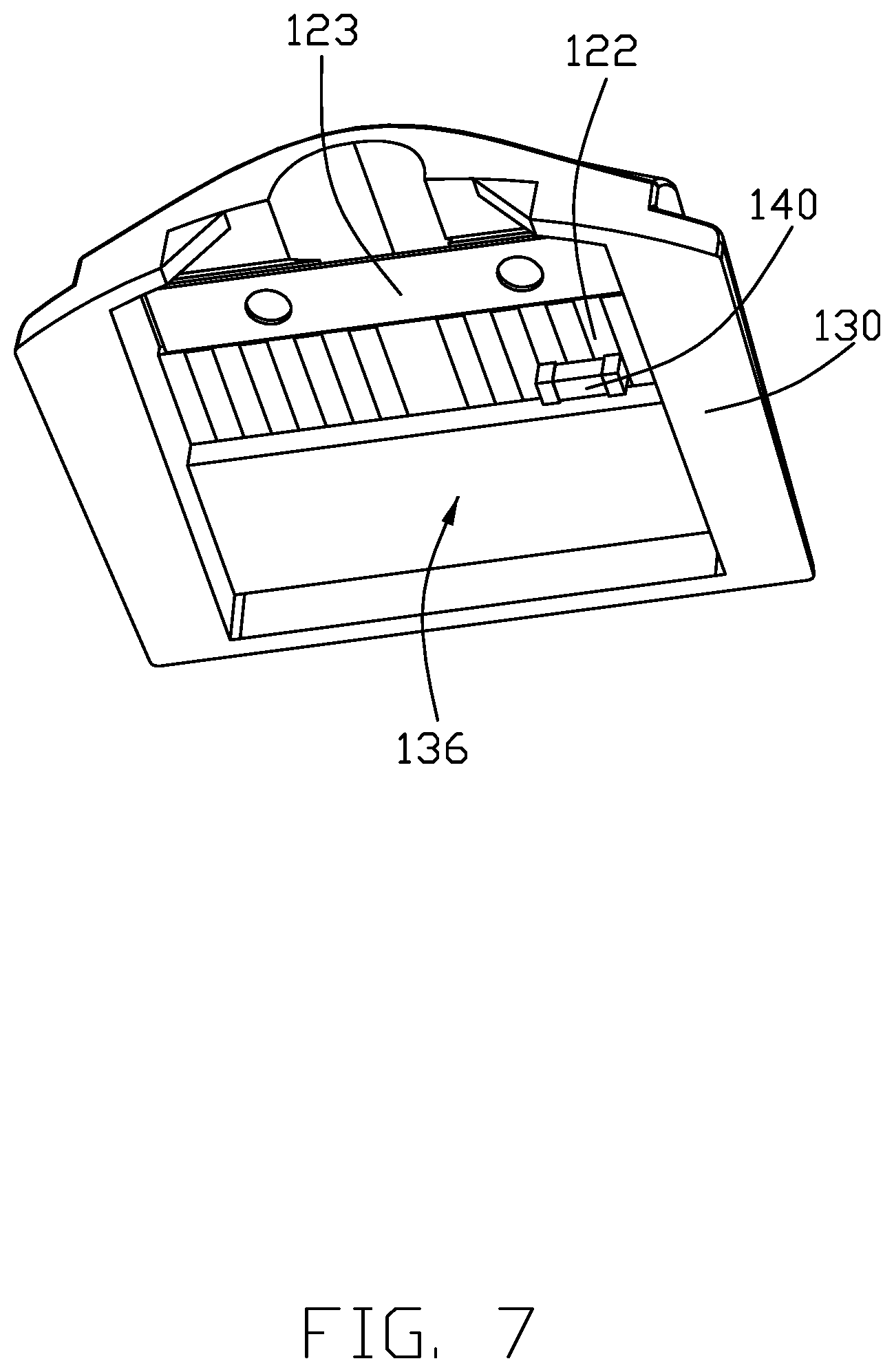
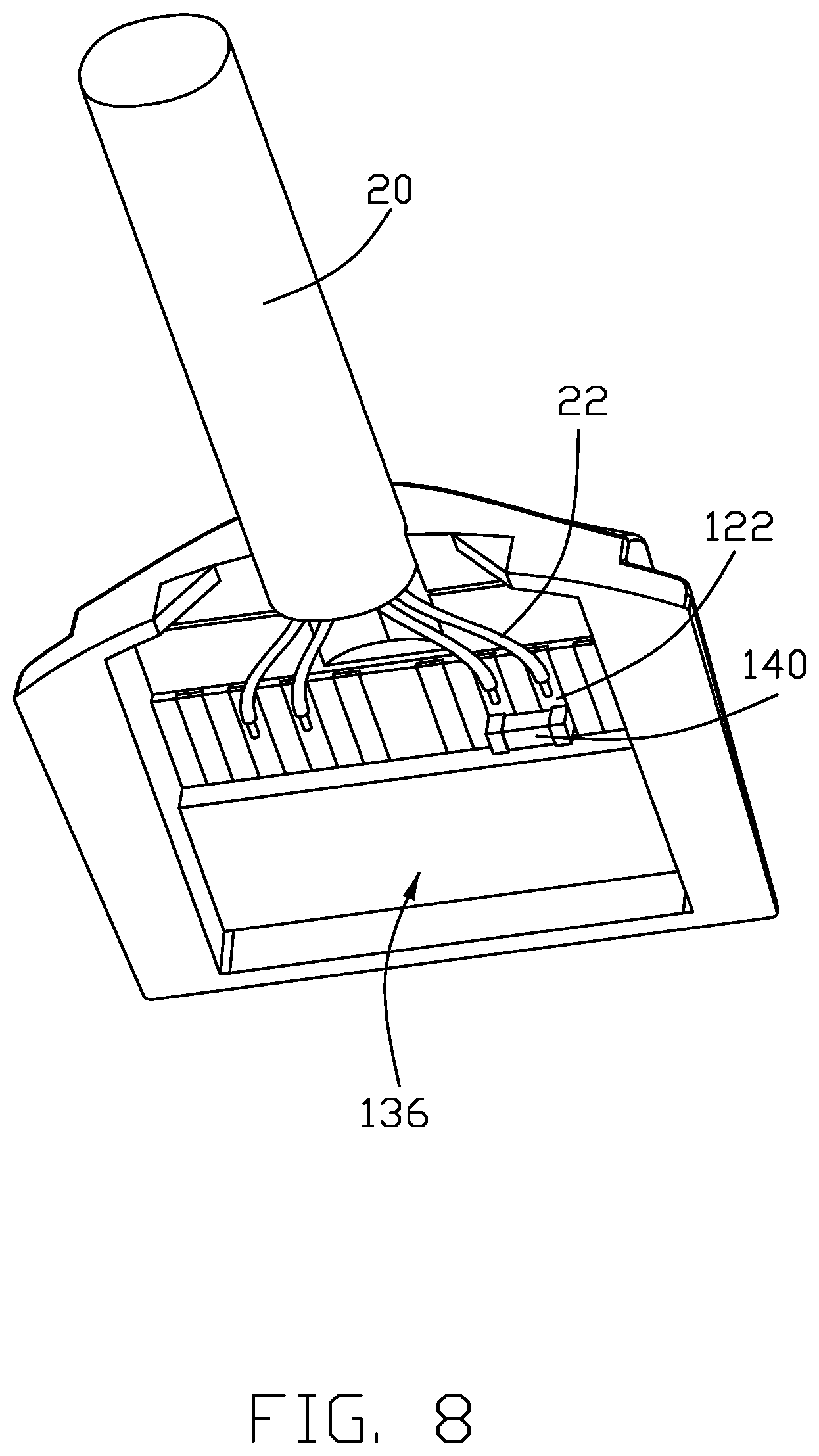
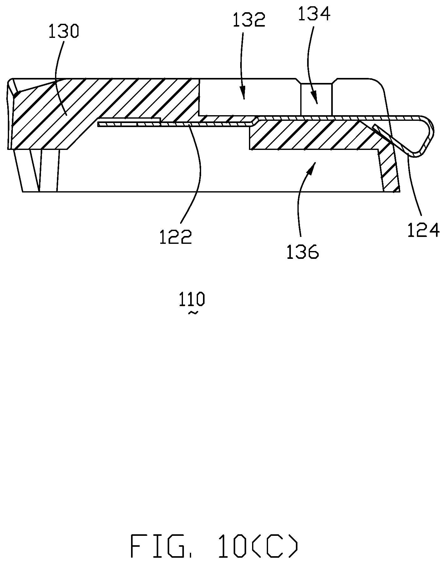
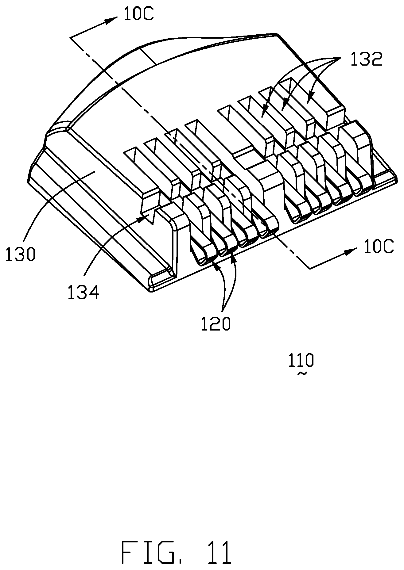
[0048] A cable assembly 10 includes a cable 20 with an electrical connector 100 at one end and a sensor sub-assembly 200 at the other end. The connector 100 includes a terminal module 110 having a plurality of contacts 120 integrally formed within an insulative housing 130 via an insert-molding process. The housing 130 forms a plurality of passageways 132 exposed to an exterior both vertically and forwardly. A transverse groove 134 extends across the passageways 132 and is exposed upon an upper surface of the housing 130. Each contact 120 includes a rear soldering section 122 exposed downwardly, an upper contacting section 124 exposed upwardly above the corresponding passageway 132, a U-shaped middle section 126 between the upper contacting section 124 and the rear soldering section 122 and within the corresponding passageway 132. The U-shaped middle section 126 includes an upper arm 125 linked to the contacting section 124, a lower arm 127 supportably seated upon the housing 130, and a bight 129 between the upper arm 125 and the lower arm 127 and within the transverse groove 134. Notably, the contact 120 initially extends along the front-to-back direction as shown in FIG. 10(A), and successively is backwardly bent to form the bight 129 via assistance of a pressing bar (not shown) which is inserted into the transverse groove 134 to downward press the contacts 120 as a fulcrum for folding the contacts 120 so as to have the contacting section 124 exposed upon the upper face of the housing 130 while being downwardly deflectable to enter the corresponding passageway 132 when the contacting section 124 is downwardly pressed by a complementary connector in the cradle part as disclosed in the aforementioned patents. Understandably. The pressing bar will be removed backwardly in the transverse direction after the U-shaped middle section 126 is formed with the final shape.
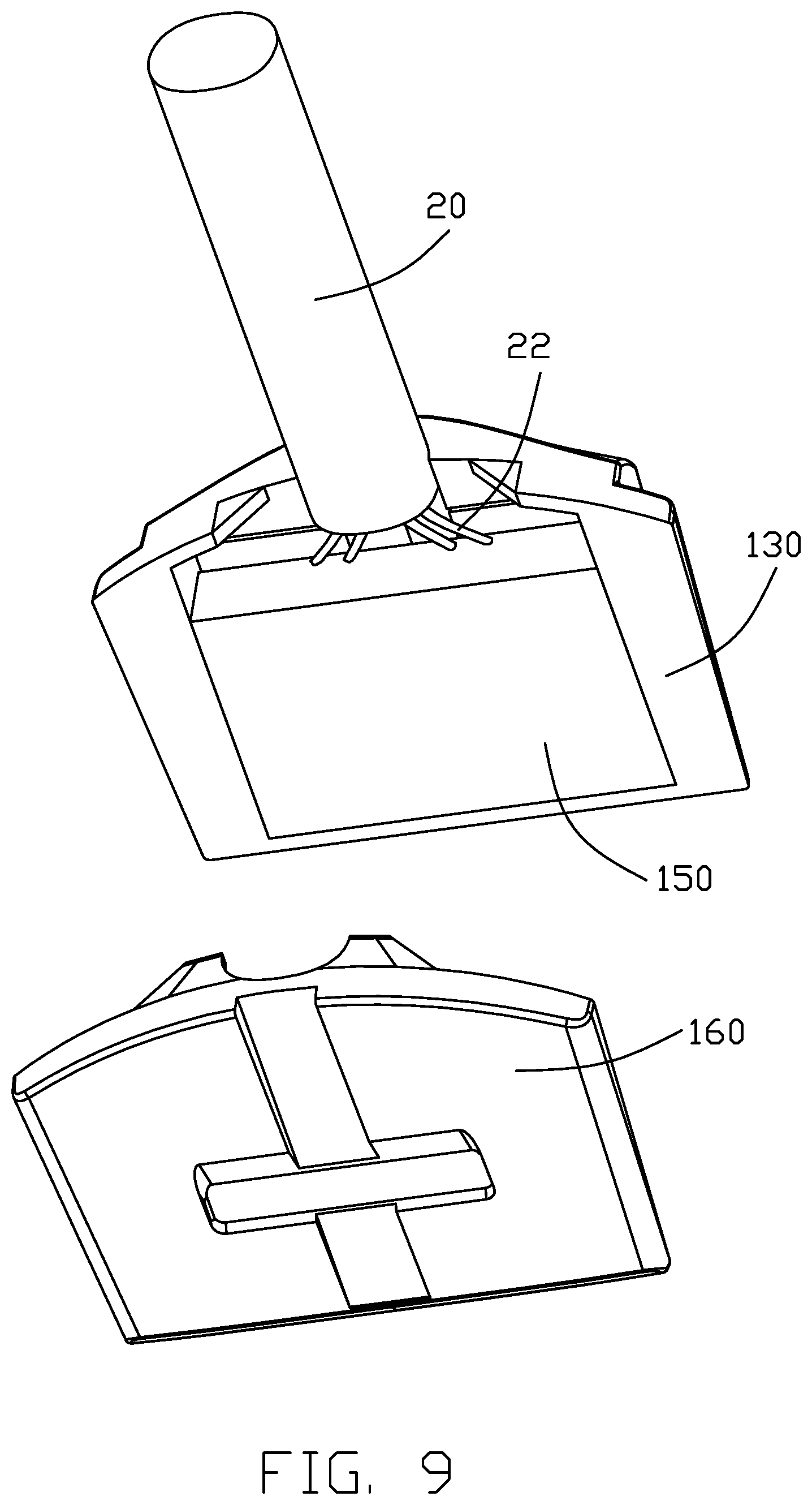
[0049] The wires 22 of the cable 20 are electrically and mechanically connected to the soldering sections 122 of the corresponding contacts 120, respectively. At least one resistor 140 is connected between soldering sections 122 of the two selected neighboring contacts 120 for regulating the corresponding power. A glue block 150 is applied upon the underside of the housing 130 to protectively cover the soldering section 122, the wires 22 and the resistor 140. Notably, because the housing 120 forms a cavity 136 in the underside, the glue block 150 can flow into and further be retained in the cavity 136 and solidified. Finally, a cap 160 is attached upon the underside of the housing 130 to cover the cavity 136.
[0050] One feature of the invention is to have the corresponding resilient contacts integrally formed with the housing for assuring waterproofing thereof. As noted, in the conventional connector the resilient contacts are required to be inserted or assembled into the corresponding passageways in the housing, thus tending to be in an inferior waterproofing state. Differently, in the invention the resilient contacts 120 are integrally formed with the housing 130 with superior waterproofing performance. Understandably, the cable assembly 10 is used with a wearable device as disclosed in the aforementioned patents, thus tending to be in a humid circumstance. Accordingly, the waterproofing function is much desired. The reason why the invention may have resilient contacts via the insert-molding process, is to provide the transverse groove 134, wherein a tool is inserted to abut against the contacts 120, to allow the originally straight type contact (as shown in FIGS. 3, 10(A), 10(C) and 11) to be backwardly bent to form the U-shaped middle section 126 (as shown in FIGS. 2(A), 4(A), 4(B) and 10(B)). Notably, the contacts 120 are originally linked to a carrier 123 in a straight manner without backward bending for insert-molding within the housing 130. After insert-molding, the carrier 123 is removed from the contacts 120 to have the wires 22 soldered upon the soldering sections 122 of the contacts 120. Notably, in this embodiment, the soldering section 122 is downward exposed for soldering to the corresponding wire 22 while the lying U-shaped middle section 126 is upwardly exposed to allow the contacting section 124 mateable with the complementary connector in the cradle (not shown) wearable on the human arm. Notably, in the conventional design, the connector is mounted upon a printed circuit board which is enclosed within a case for grasping and linked to the wires of the cable assembly, wherein the resistor is mounted upon the printed circuit board. In this invention, the resistor is directly soldered upon the contact tails, thus being unnecessary to provide the printed circuit board. Understandably, in this embodiment the housing 130 is unitary so as to assure the superior waterproofing performance while alternately the terminal module including the contacts integrally formed within an insulator, may be discrete from and assembled to the remaining housing for easing manufacturing.
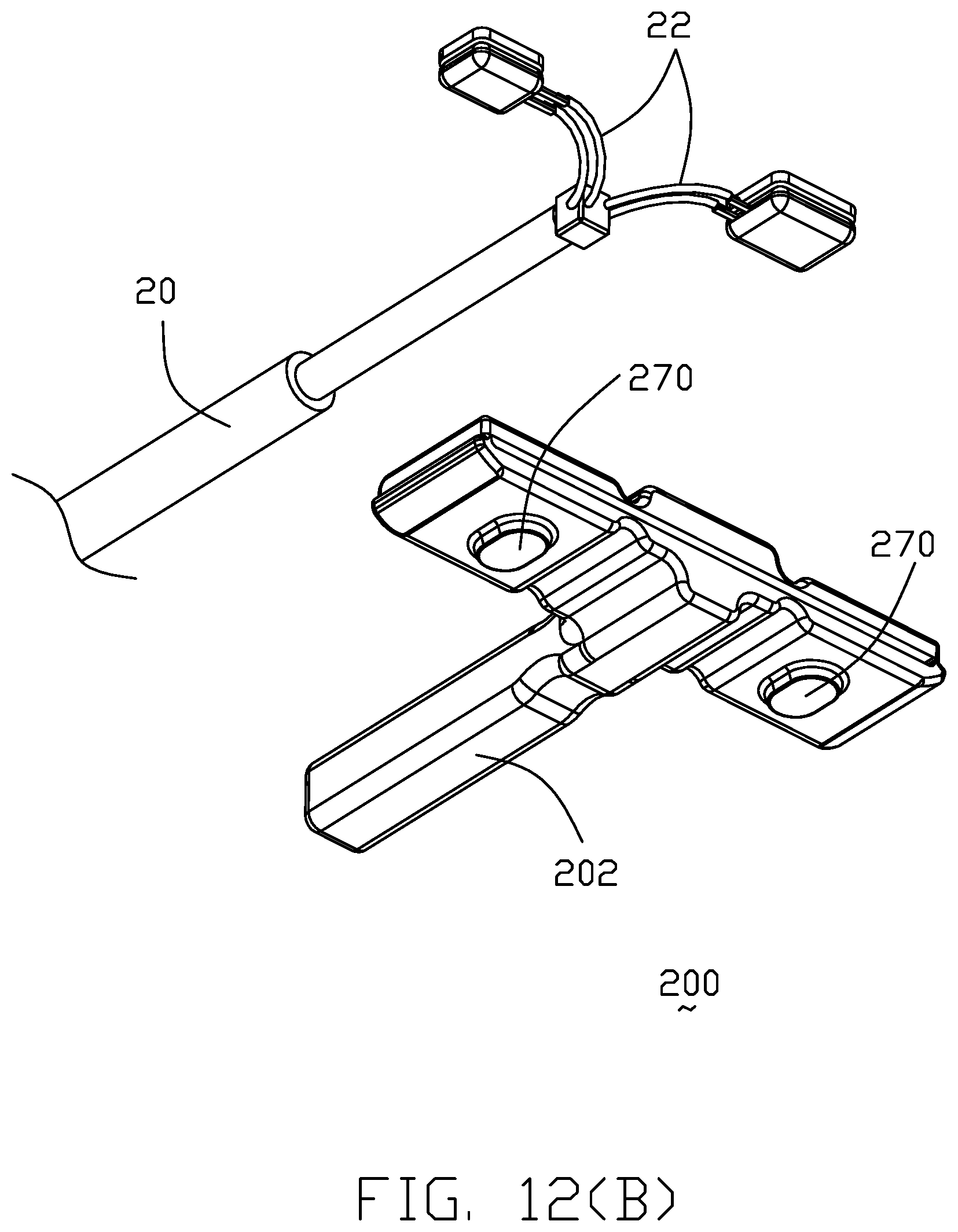
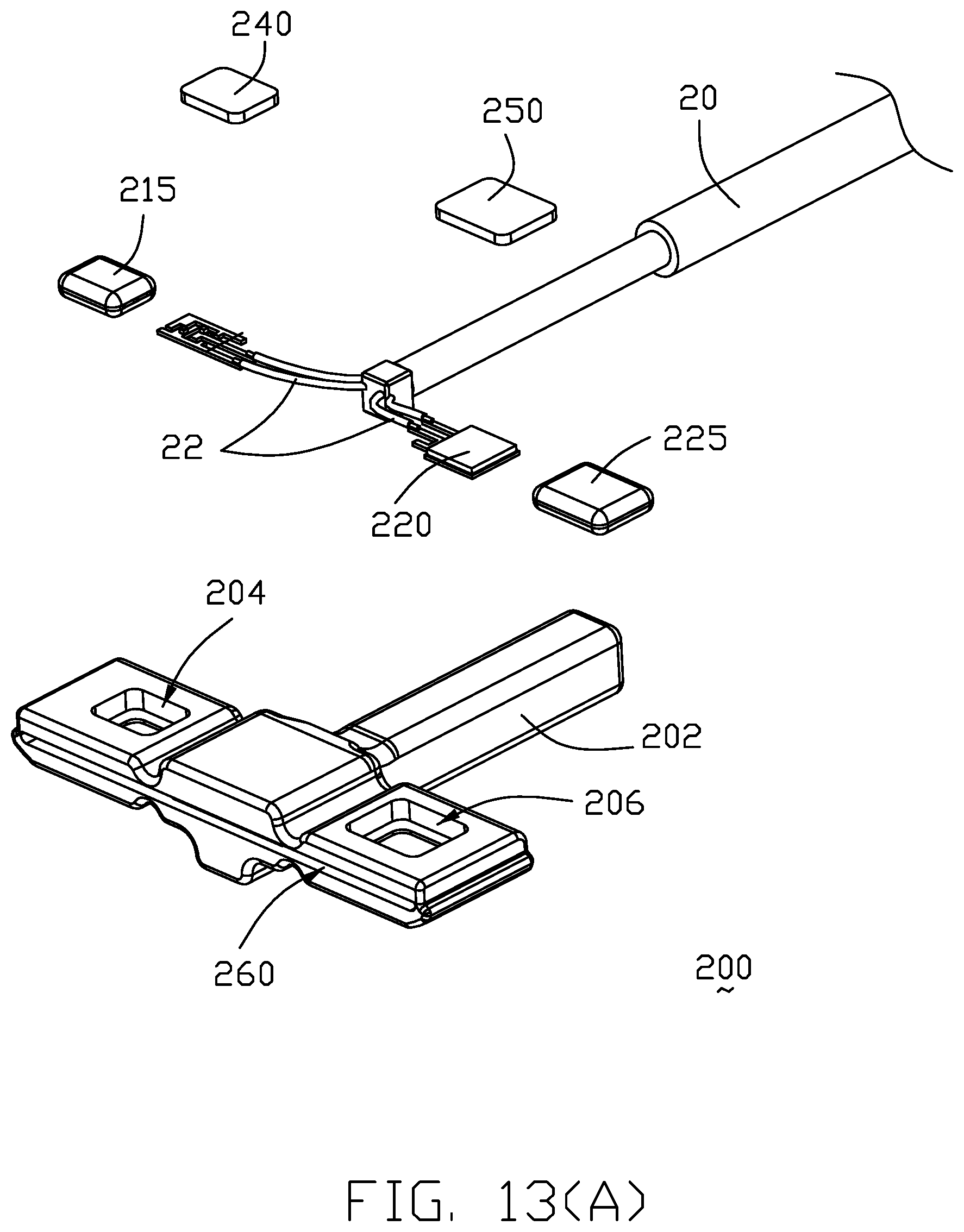
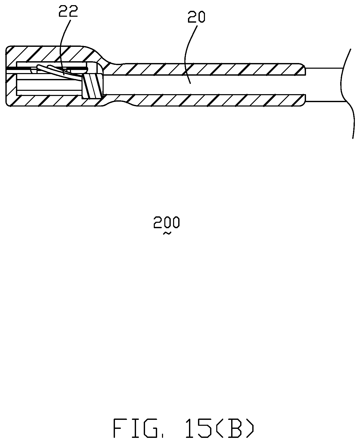
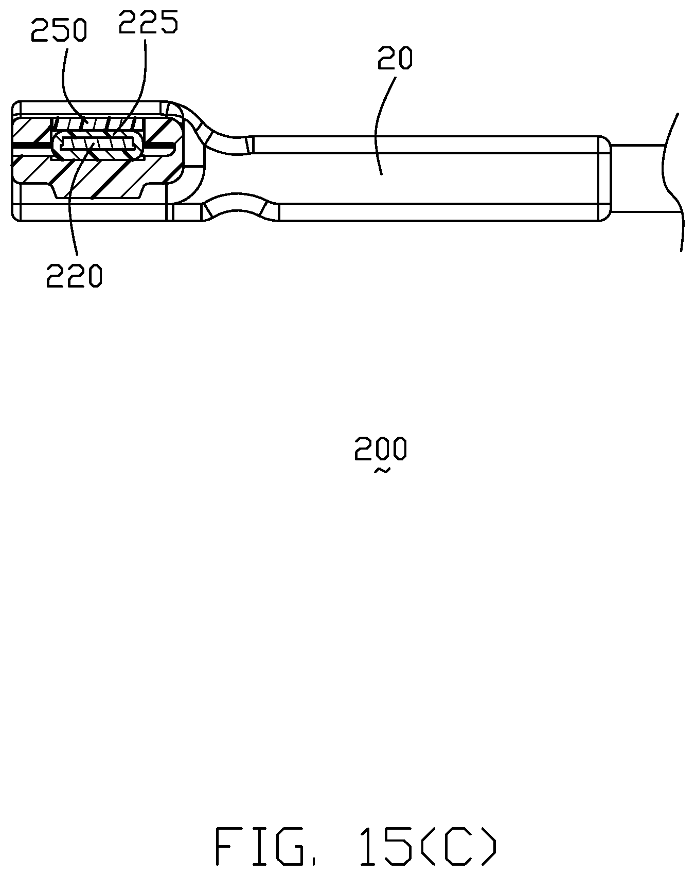
[0051] The sensor sub-assembly 200 includes a T-shaped overmolded insulative housing 202 receiving an LED (Light Emitting Diode) enclosed within the LED housing 215 with the corresponding contacts 212 mechanically and electrically connected to the corresponding wires 22, and a PD (Photo Diode) 220 enclosed within the PD housing 225 with the corresponding contacts 222 electrically and mechanically connected to the corresponding wire 22. Notably, the housing 202 has an LED cavity 204 receiving the LED housing 215 and the LED lens cover 240 atop the LED housing 215 to, and a PD cavity 206 receiving the PD housing 225 and the PD lens cover 250 atop the PD housing 225. A transverse slot 260 communicates with both the LED housing 215 and the PD housing 225 and is filled with the silicon after both the LED housing 215 and the PD housing 225 are assembled within the housing 202. The housing 202 further unitarily forms a pair of features/projections 270 for locating consideration.
[0052] Compared with the conventional design, the sensor sub-assembly 200 is equipped with the LED and the PD without involvement of the FPC (Flexible Printed Circuit) in a robust arrangement.
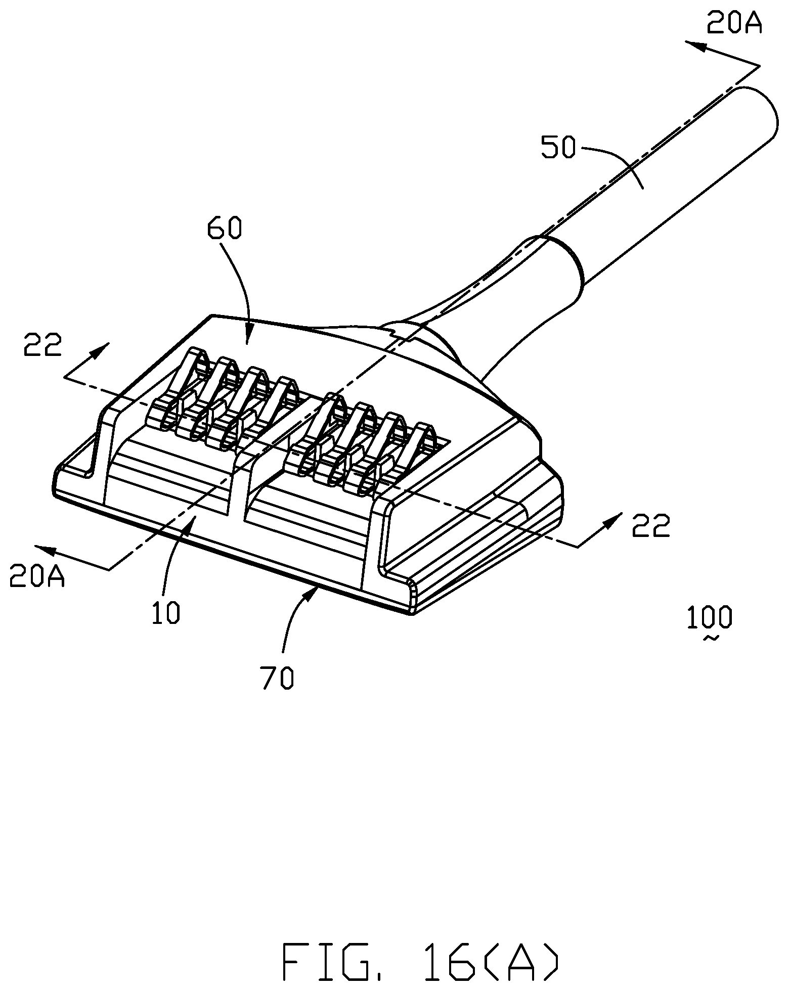
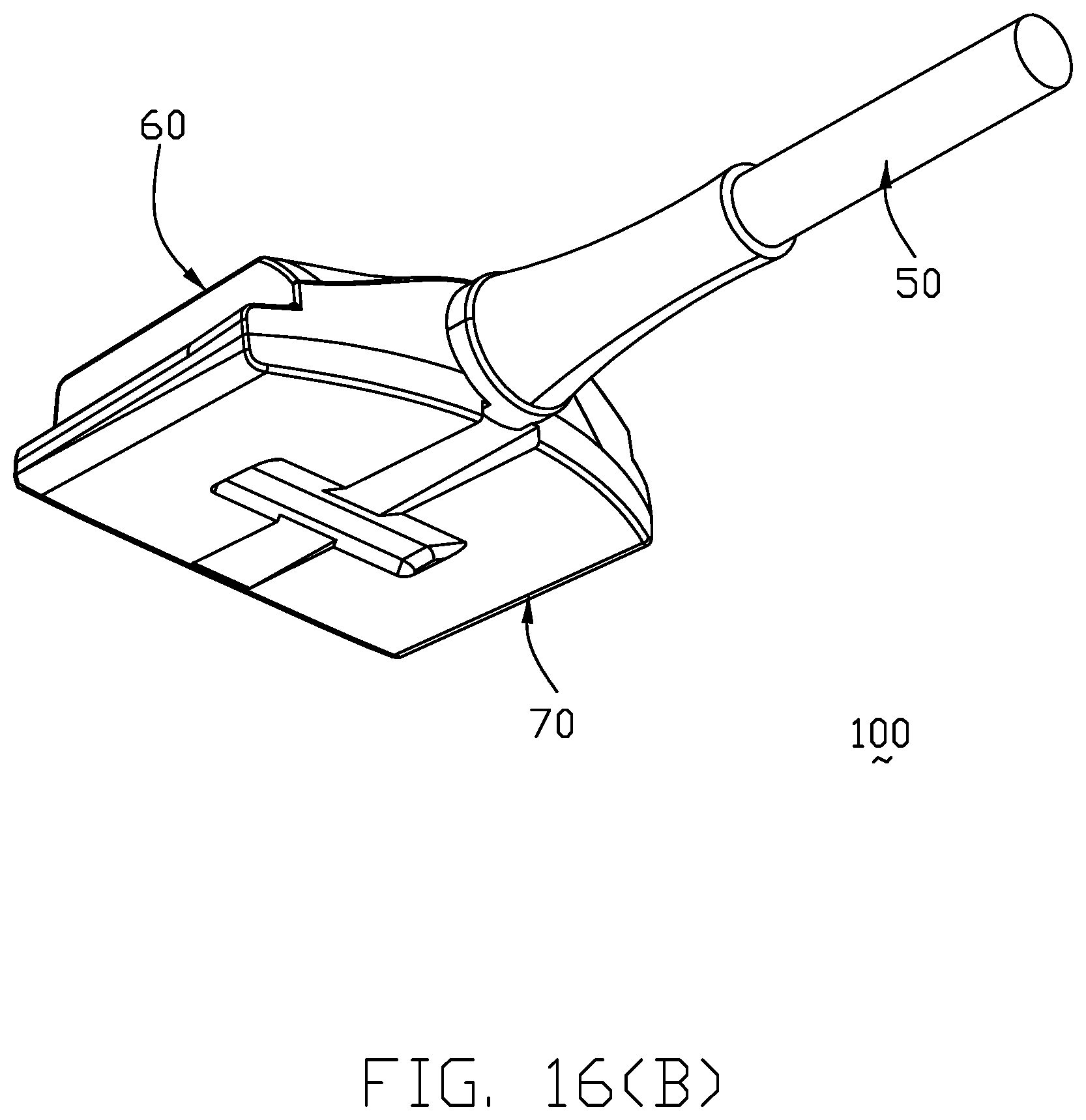
[0053] As shown in FIGS. 16(A)-22, a cable connector assembly 100 includes a contact module 10 sandwiched between an upper cover 60 and a lower cover 70 in the vertical direction. The contact module 10 includes a plurality of contacts 20 integrally formed within an insulator 40 via an insert-molding process. Each contact 20 includes a lower stationary horizontal section 22 and an upper deflectable/resilient curved contacting section 24 linked by a bight 26 therebetween. The horizontal section 22 is divided into a front region 28 and a rear region 30. A lance 32 is stamped out from the front region 28 to form an opening 34 therein corresponding. A tab 36 is located at the free end of the contacting section 24. The insulator 40 forms an exposed curved mating port 42 with a plurality of ribs 44 thereon. The contacting sections 24 are exposed upon the mating port 42 and separated from one another via the ribs 44. Notably, the opening 34 is filled with the material of the insulator 40, and the lance 32 is embedded within the insulator 40. The insulator 40 forms a crossbar 46 at a rear portion.
[0054] A cable 50 is located behind the contact module 10 and includes a strain relief 52 disposed in the corresponding cavities 61, 71 formed by the upper cover 60 and the lower cover 70. The upper cover 60 forms a transverse bar 62 abutting against the crossbar 46 in the vertical direction. The upper cover 60 further forms at each lateral side a step structure 64 to downwardly press the corresponding lateral side region of the contact module 10. Therefore, the contact module 10 can not move upwardly due to the step structure 64 and the transverse bar 62. Similarly, an upward structure 72 is formed on an inner surface of the lower cover 70 to upwardly support an underside of the contact module 10. Therefore, the contact module 10 can be stably retained between the upper cover 60 and the lower cover 70. Understandably, the contact 20 originally extends along the front-to-back direction when the contact module 10 is made via the insert-molding process, and the contacting section 24 is backwardly folded via the bight 26 after the contact module 10 is formed to be in a deflectable manner in the vertical direction perpendicular to the front-to-back direction. The tab 36 is downwardly pressed by the flange 68 of the upper cover 60 in a preloaded manner. As shown in FIGS. 20(A) and 20(B), even though the tab 36 is spaced from the horizontal section 22 of the corresponding contact 20 in the vertical direction when the connector assembly 100 is un-mated, such a tab 36 is downwardly moved to contact an upper side of the horizontal section 22 of the corresponding contact 20 during mating so as to result in another/shorter circuit path in addition to the original one via the bight 26 for superior signal transmission.
[0055] The upper cover 60 forms a pair of vertical side walls 66 while the insulator 40 of the contact module 10 forms a vertical center wall 48 having the similar configuration with the vertical side walls 66 so as to form two areas in which the contacts 20 are disposed with equal amounts. The cable 50 includes a plurality of wires 54 respectively soldered upon undersides of the rear regions 30 of the corresponding contacts 20. Notably, FIG. 21(A) shows the upper side of the horizontal section 22 is essentially upwardly exposed to the exterior except the lance 32 which is hidden under the opening 34 filled by the insulator 40,
[0056] While a preferred embodiment in accordance with the present disclosure has been shown and described, equivalent modifications and changes known to persons skilled in the art according to the spirit of the present disclosure are considered within the scope of the present disclosure as described in the appended claims.
* * * * *
D00000
D00001
D00002
D00003
D00004
D00005
D00006
D00007
D00008
D00009
D00010
D00011
D00012
D00013

D00014

D00015
D00016
D00017

D00018
D00019
D00020
D00021
D00022
D00023
D00024
D00025
D00026
D00027
D00028
D00029

D00030
D00031
D00032

D00033
D00034

D00035
D00036
D00037
D00038
D00039
XML
uspto.report is an independent third-party trademark research tool that is not affiliated, endorsed, or sponsored by the United States Patent and Trademark Office (USPTO) or any other governmental organization. The information provided by uspto.report is based on publicly available data at the time of writing and is intended for informational purposes only.
While we strive to provide accurate and up-to-date information, we do not guarantee the accuracy, completeness, reliability, or suitability of the information displayed on this site. The use of this site is at your own risk. Any reliance you place on such information is therefore strictly at your own risk.
All official trademark data, including owner information, should be verified by visiting the official USPTO website at www.uspto.gov. This site is not intended to replace professional legal advice and should not be used as a substitute for consulting with a legal professional who is knowledgeable about trademark law.