System and Method for Converting Chemical Energy Into Electrical Energy Energy Using Nano-Engineered Porous Network Materials
GIDWANI; Jawahar ; et al.
U.S. patent application number 16/782199 was filed with the patent office on 2020-06-04 for system and method for converting chemical energy into electrical energy energy using nano-engineered porous network materials. This patent application is currently assigned to QuSwami, Inc.. The applicant listed for this patent is QUSWAMI, INC.. Invention is credited to Jawahar GIDWANI, Arash HAZEGHI, Attila HORVATH, Andrew LAM.
| Application Number | 20200176798 16/782199 |
| Document ID | / |
| Family ID | 48948529 |
| Filed Date | 2020-06-04 |


View All Diagrams
| United States Patent Application | 20200176798 |
| Kind Code | A1 |
| GIDWANI; Jawahar ; et al. | June 4, 2020 |
System and Method for Converting Chemical Energy Into Electrical Energy Energy Using Nano-Engineered Porous Network Materials
Abstract
An energy conversion device for conversion of chemical energy into electricity. The energy conversion device has a first and second electrode. A substrate is present that has a porous semiconductor or dielectric layer placed thereover. The porous semiconductor or dielectric layer can be a nano-engineered structure. A porous catalyst material is placed on at least a portion of the porous semiconductor or dielectric layer such that at least some of the porous catalyst material enters the nano-engineered structure of the porous semiconductor or dielectric layer, thereby forming an intertwining region.
| Inventors: | GIDWANI; Jawahar; (San Francisco, CA) ; HAZEGHI; Arash; (San Francisco, CA) ; LAM; Andrew; (San Francisco, CA) ; HORVATH; Attila; (Berkeley, CA) | ||||||||||
| Applicant: |
|
||||||||||
|---|---|---|---|---|---|---|---|---|---|---|---|
| Assignee: | QuSwami, Inc. San Francisco CA |
||||||||||
| Family ID: | 48948529 | ||||||||||
| Appl. No.: | 16/782199 | ||||||||||
| Filed: | February 5, 2020 |
Related U.S. Patent Documents
| Application Number | Filing Date | Patent Number | ||
|---|---|---|---|---|
| 15130386 | Apr 15, 2016 | 10573913 | ||
| 16782199 | ||||
| 13945864 | Jul 18, 2013 | 9437892 | ||
| 15130386 | ||||
| 61724764 | Nov 9, 2012 | |||
| 61716889 | Oct 22, 2012 | |||
| 61712712 | Oct 11, 2012 | |||
| 61676285 | Jul 26, 2012 | |||
| Current U.S. Class: | 1/1 |
| Current CPC Class: | H01M 8/1004 20130101; H01M 8/22 20130101; H01M 4/8657 20130101; H01M 4/8652 20130101; B82Y 30/00 20130101; H01M 8/10 20130101; H01M 4/925 20130101; H01M 8/225 20130101; H01M 4/8647 20130101; H01M 14/00 20130101; Y02E 60/50 20130101; H01M 4/8605 20130101; H01M 4/92 20130101; H01M 4/8626 20130101; H01M 4/9025 20130101 |
| International Class: | H01M 8/10 20060101 H01M008/10; H01M 8/1004 20060101 H01M008/1004; H01M 4/86 20060101 H01M004/86; H01M 14/00 20060101 H01M014/00; B82Y 30/00 20060101 B82Y030/00 |
Claims
1. An energy conversion device for conversion of chemical energy into electricity, comprising: a first electrode; a substrate connected to said first electrode; a three-dimensioned textured porous semiconductor layer disposed over said substrate, said three-dimensioned textured porous semiconductor layer having a nano-engineered structure; a porous catalyst material on at least a portion of said three-dimensioned textured porous semiconductor layer that contacts a fuel and an oxidizer, wherein at least some of the porous catalyst material enters the nano-engineered structure of said three-dimensioned textured porous semiconductor layer to form an intertwining region, the porous catalyst material and the three-dimensioned textured porous semiconductor layer forming solid-state junctions, wherein the solid-state junctions are p-n junctions; and a second electrode, wherein electrons from the porous catalyst material are injected into the three-dimensioned textured porous semiconductor layer, and wherein an electrical potential is formed between the first electrode and a second electrode during chemical reactions between the fuel and oxidizer in contact with the porous catalyst material.
2. The energy conversion device of claim 1, wherein the substrate is patterned to create a three-dimensional surface, thereby providing increased surface area for chemical reactions.
3. The energy conversion device of claim 2, wherein the substrate is patterned such that nano-wires are formed.
4. The energy conversion device of claim 2, wherein the substrate is textured such that peaks and valleys are formed.
5. The energy conversion device of claim 1, further comprising a non-porous semiconductor layer is in between the substrate and the three-dimensioned textured porous semiconductor layer
6. The energy conversion device of claim 1, wherein the porous catalyst layer is formed with nano-particles.
7. The energy conversion device of claim 1, wherein the porous catalyst layer is formed with nano-clusters.
8. The energy conversion device of claim 1, wherein the porous catalyst layer is formed with nano-wires.
9. The energy conversion device of claim 1, wherein the three-dimensioned textured porous semiconductor layer is formed with nano-particles.
10. The energy conversion device of claim 1, wherein the three-dimensioned textured porous semiconductor layer is formed with nano-clusters.
11. The energy conversion device of claim 1, wherein the three-dimensioned textured porous semiconductor layer is formed with nano-wires.
12. The energy conversion device of claim 1, wherein the three-dimensioned textured porous semiconductor layer is a porous nano-engineered structure with percolating networks.
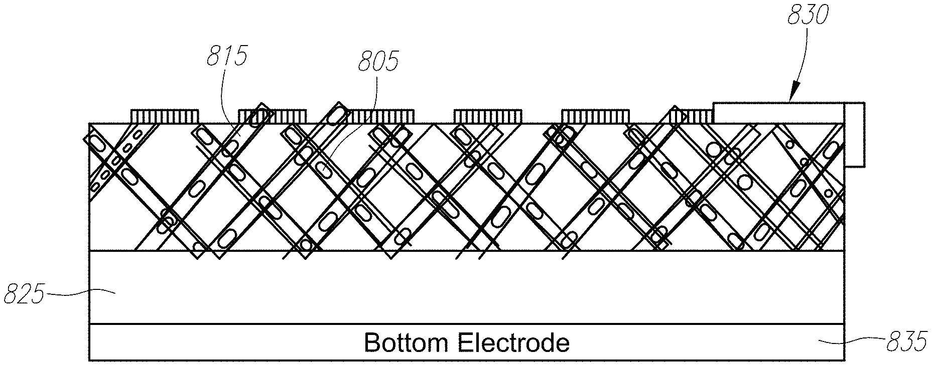
13. The energy conversion device of claim 1, wherein the three-dimensioned textured porous semiconductor layer comprises a dielectric.
14. The energy conversion device of claim 13, wherein the dielectric is a porous nano-engineered structure with percolating networks.
15. The energy conversion device of claim 13, wherein the dielectric is formed with nano-particles.
16. The energy conversion device of claim 13, wherein the dielectric is formed with nano-clusters.
17. The energy conversion device of claim 13, wherein the dielectric is formed with the nano-wires.
18. The energy conversion device of claim 1, where the three-dimensioned textured porous semiconductor layer are chosen from a group including rutile Ti02, anatase Ti02, poly-crystalline Ti0.sub.2 porous Ti02, Zr02, SrTi0.sub.3, BaTi03, Sr_x-Ba_y-TiO_z, LiNiO, silicon, SiC, GaN, GaAs, Ge, silica, carbon, oxides of niobium, tantalum, zirconium, cerium, tin, vanadium, and LaSrV03, and certain organic semiconductors, such as PTCDA, or 3,4,9,10-perylenetetracarboxylicacid-dianhydride.
19. An energy conversion device for conversion of chemical energy into electricity, comprising: a first electrode; a substrate connected to said first electrode; a three-dimensioned textured porous semiconductor layer disposed over said substrate, said three-dimensioned textured porous semiconductor layer having a nano-engineered structure; a porous catalyst material on at least a portion of said three-dimensioned textured porous semiconductor layer, wherein at least some of the porous catalyst material enters the nano-engineered structure of the three-dimensioned textured porous semiconductor layer to form an intertwining region, the porous catalyst material and the three-dimensioned textured porous semiconductor layer forming solid-state junctions, wherein the solid-state junctions are Schottky junctions; and a second electrode, wherein electrons from the porous catalyst material are injected into the three-dimensioned textured porous semiconductor layer, and wherein an electrical potential is formed between the first electrode and a second electrode during chemical reactions between a fuel, the porous catalyst material and the three-dimensioned textured porous semiconductor layer.
20. The energy conversion device of claim 19, wherein the substrate is patterned to create a three-dimensional surface, thereby providing increased surface area for chemical reactions.
21. The energy conversion device of claim 20, wherein the substrate is patterned such that nano-wires are formed.
22. The energy conversion device of claim 20, wherein the substrate is textured such that peaks and valleys are formed.
23. The energy conversion device of claim 19, further comprising a non-porous semiconductor layer is in between the substrate and the three-dimensioned textured porous semiconductor layer
24. The energy conversion device of claim 19, wherein the porous catalyst layer is formed with nano-particles.
25. The energy conversion device of claim 19, wherein the porous catalyst layer is formed with nano-clusters.
26. The energy conversion device of claim 19, wherein the porous catalyst layer is formed with nano-wires.
27. The energy conversion device of claim 19, wherein the three-dimensioned textured porous semiconductor layer is formed with nano-particles.
28. The energy conversion device of claim 19, wherein the three-dimensioned textured porous semiconductor layer is formed with nano-clusters.
29. The energy conversion device of claim 19, wherein the three-dimensioned textured porous semiconductor layer is formed with nano-wires.
30. The energy conversion device of claim 19, wherein the three-dimensioned textured porous semiconductor layer is a porous nano-engineered structure with percolating networks.
31. The energy conversion device of claim 19, wherein the three-dimensioned textured porous semiconductor layer comprises a dielectric.
32. The energy conversion device of claim 31, wherein the dielectric is a porous nano-engineered structure with percolating networks.
33. The energy conversion device of claim 31, wherein the dielectric is formed with nano-particles.
34. The energy conversion device of claim 31 wherein the dielectric is formed with nano-clusters.
35. The energy conversion device of claim 31, wherein the dielectric is formed with the nano-wires.
36. The energy conversion device of claim 19, where the three-dimensioned textured porous semiconductor layer are chosen from a group including rutile Ti02, anatase Ti02, poly-crystalline Ti0.sub.2 porous Ti02, Zr02, SrTi0.sub.3, BaTi03, Sr_x-Ba_y-TiO_z, LiNiO, silicon, SiC, GaN, GaAs, Ge, silica, carbon, oxides of niobium, tantalum, zirconium, cerium, tin, vanadium, and LaSrV0.sub.3, and certain organic semiconductors, such as PTCDA, or 3,4,9,10-perylenetetracarboxylicacid-dianhydride.
37. The energy conversation device of claim 1, wherein the fuel and the oxidizer comprise a monopropellant.
Description
CROSS-REFERENCE TO RELATED APPLICATIONS
[0001] This application is a continuation of U.S. patent application Ser. No. 15/130,386, filed Apr. 15, 2016, now U.S. patent Ser. No. ______, which is a continuation of U.S. patent application Ser. No. 13/945,864 filed Jul. 18, 2013. Priority to these patent applications is expressly claimed, and the disclosure thereof is hereby incorporated herein by reference in its entirety. This application claims the benefit of Provisional Application Nos. 61/676,285 filed Jul. 26, 2012, 61/712,712 filed Oct. 11, 2012, 61/716,889 filed Oct. 22, 2012, and 61/724,764 filed Nov. 9, 2012. Priority to these provisional applications is expressly claimed, and the disclosures of the provisional applications are hereby incorporated herein by reference in their entirety.
FIELD
[0002] This patent document relates generally to energy conversion systems and more particularly relates to a method and system for converting chemical energy into electrical power using solid-state electric generators using planar or three dimensional surfaces that comprise porous material networks such as a nano-wire arrays or nano-engineered structures, or nano-particles, or colloidal paste.
BACKGROUND
[0003] The use of solid state electric generators to convert chemical energy into electricity has recently been demonstrated, as explained, for example, in U.S. Pat. Nos. 6,268,560, 6,649,823, 7,371,962, and 7,663,053. U.S. Pat. Nos. 6,268,560, 6,649,823, 7,371,962, and 7,663,053 are hereby incorporated herein by reference in their entirety. Such energy conversion devices efficiently convert chemical energy to electricity. For example, FIG. 1 herein illustrates a solid state electric generator along with graphs showing characteristics of such a device. As shown in cross section in FIG. 1-A herein, a charge carrier, usually an electron e.sup.-, is energized on or near a conducting surface 10A by an energizer 12A. The charge carrier is energized, for example, by chemical reactions. In each case the charge carrier is injected into a semiconductor conduction band. For example, the charge carrier ballistically moves from a conductor 10A into a semiconductor or dielectric 11A. The conductor 10A is so thin that the electron effectively travels through it ballistically, without losing energy or colliding with another electron or atom. Since an energy offset exists between the semiconductor conduction band and the Fermi level of the catalyst, the result is a voltage 14A across positive terminal 17A and negative terminal 16A. In FIG. 1-A, the dielectric junction 15A is a semiconductor junction specifically chosen to create an electrical potential voltage barrier which tends to impede the electron ballistic motion, shown as 11B in FIG. 1-B. FIG. 1-B shows the electrical potential in the device as a function of distance along the device at zero bias.
[0004] The potential voltage barrier can be formed in any one of many ways, for example, a Schottky barrier as shown in FIG. 1-C, a p-n junction in FIG. 1-D, or a conductor-dielectric-conductor junction, FIG. 1-E. The dielectric is electrically conductive. A forward biased diode provides one of the simplest methods to implement this energy converting device. FIG. 1-C depicts a forward biased Schottky diode whose positive terminal is a conductor/metal.
SUMMARY
[0005] The present patent document describes various embodiments having novel three dimensional device structures that can be on a planar two-dimensional substrate or on a three-dimensional substrate. The various embodiments improve on earlier solid state electric generators by increasing amount of power (i.e., electricity) that can be produced per unit of two-dimensional area of a device. The novel device structures described herein have solid-state junctions. These device structures comprise porous semiconductor or dielectrics and nano-clusters of conductor and/or catalyst to form the solid-state junctions. Even though there are voids in the composite system, different porous semiconductor/catalyst materials, as an example, can be an integrated system or the materials may be physically connected as a network. Nano-clusters are when materials form nano-sized clusters. The solid-state junctions can be, but are not limited to, Schottky diodes or p-n junctions. Also disclosed are methods/processes to fabricate the disclosed device structures, specifically for converting chemical energy directly into electrical potential to produce power.
[0006] An energy conversion device for conversion of chemical energy into electricity is disclosed. A first aspect of the energy conversion device comprises a first electrode connected to a substrate. A porous semiconductor (or dielectric) layer is disposed over the substrate (with an optional non-porous semiconductor (or dielectric) layer being in-between the substrate on the porous semiconductor (or dielectric) layer. A porous catalyst material is located on at least a portion of the porous semiconductor (or dielectric) layer. At least some of the porous catalyst material enters the nano-engineered structure of the porous semiconductor layer, which forms an intertwining region. A second electrode is present, and an electrical potential is formed between the first electrode and a second electrode during chemical reactions between a fuel, the porous catalyst material, and the porous semiconductor network.
[0007] In another aspect disclosed herein, the substrate of the energy conversion device is patterned to create a three-dimensional surface, thereby providing increased surface area for chemical reactions.
[0008] In another aspect disclosed herein, the substrate of the energy conversion device is patterned such that nano-wires are formed.
[0009] In another aspect disclosed herein, the substrate of the energy conversion device is textured such that peaks and valleys are formed.
[0010] In another aspect disclosed herein, the energy conversion device has a non-porous semiconductor layer in between the substrate and the porous semiconductor layer.
BRIEF DESCRIPTION OF THE DRAWINGS
[0011] The accompanying drawings, which are included as part of the present specification, illustrate various embodiments and together with the general description given above and the detailed description of the embodiments given below serve to explain and teach the principles described herein.
[0012] FIG. 1-A illustrates a solid-state electric generator.
[0013] FIG. 1-B illustrates a graph of potential energy versus distance from the device's topmost surface and indicating the effect of a potential barrier in a solid-state junction.
[0014] FIG. 1-C illustrates a graph of potential versus distance from the device's topmost surface in an exemplary solid-state electric generator having a Schottky barrier.
[0015] FIG. 1-D illustrates a graph of potential versus distance from the device's topmost surface in an exemplary solid-state electric generator having a p-n junction potential barrier.
[0016] FIG. 1-E illustrates a graph of potential versus distance from the device's topmost surface in an exemplary solid-state electric generator having a conductor-dielectric-conductor potential barrier.
[0017] FIG. 2 illustrates the energy band diagram for a catalyst-semiconductor interface
[0018] FIG. 3 illustrates the schematics of EMF generation mechanism
[0019] FIG. 4 illustrates a schematic cross-section of a portion of a nanowire material array with a catalyst network.
[0020] FIG. 5a depicts a cross-sectional view of a three-dimensional porous network which consists of a porous catalyst three-dimensional layer that intertwines three-dimensionally with another porous semiconductor or dielectric three-dimensional layer on a planar two-dimensional substrate. A non-porous interlayer can optionally be inserted between the planar substrate and the porous three-dimensional layers/networks above.
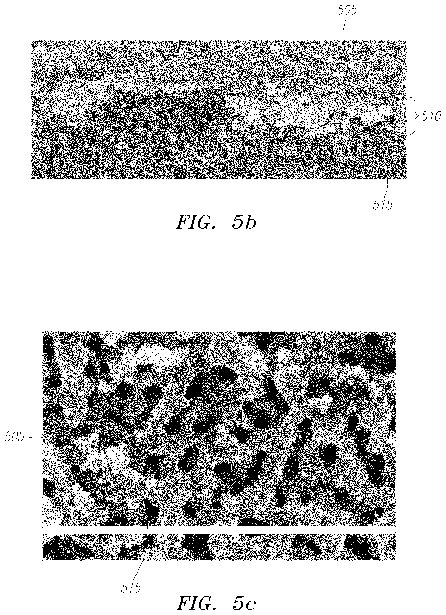
[0021] FIG. 5b is a cross-sectional microscopic view of a three-dimensional porous network which consists of a porous catalyst three-dimensional layer that intertwines three-dimensionally with another porous semiconductor or dielectric three-dimensional layer.
[0022] FIG. 5c is a top microscopic image of an energy converter having a three-dimensional porous network which consists of a porous catalyst three-dimensional layer that intertwines three-dimensionally with another porous semiconductor or dielectric three-dimensional layer.
[0023] FIG. 6 shows an energy converter having a multi-cell device structure with multiple layers of three-dimensional porous catalyst and three-dimensional porous semiconductor or dielectric networks on a planar substrate. A non-porous interlayer can be inserted or not between the planar two-dimensional substrate and the porous three-dimensional layers/networks above.
[0024] FIG. 7 shows an exemplary energy converter having a patterned three-dimensional network of porous catalyst and porous semiconductor or dielectric on a three-dimensional substrates, in which the internal and external surfaces are covered with a porous semiconductor or dielectric layer/network that intertwines with a porous catalyst layer/network three-dimensionally. An optional non-porous layer can also be inserted between the three-dimensional substrates and the three-dimensional catalyzed porous semiconductor or dielectric layer/network.
[0025] FIG. 8 shows an exemplary energy converter having three-dimensional porous substrate/supporting layer (partially or fully) network of porous catalyst and porous semiconductor or dielectric on a three-dimensional substrates, in which the internal and external surfaces are covered with a porous semiconductor or dielectric layer/network that intertwines with a porous catalyst layer/network three-dimensionally. An optional non-porous layer can also be inserted between the three-dimensional substrates and the three-dimensional catalyzed porous semiconductor or dielectric layer/network.
[0026] FIG. 9a shows an exemplary energy converter having a textured three-dimensional network of porous catalyst and porous semiconductor or dielectric on a three-dimensional substrates, in which the internal and external surfaces are covered with a porous semiconductor or dielectric layer/network that intertwines with a porous catalyst layer/network three-dimensionally. An optional non-porous layer can also be inserted between the three-dimensional substrates and the three-dimensional catalyzed porous semiconductor or dielectric layer/network.
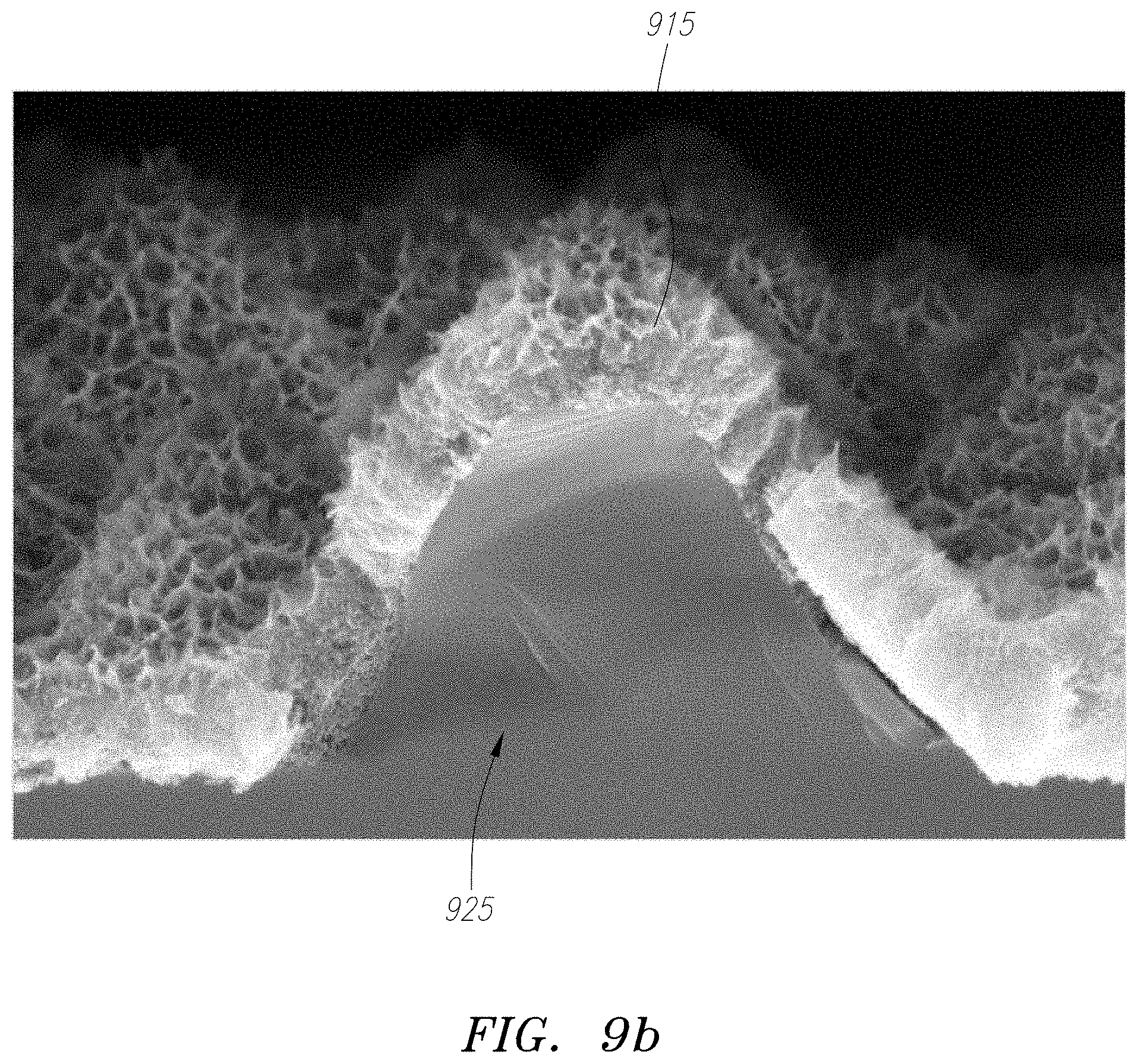
[0027] FIG. 9b is a microscopic image of a cross section of an exemplary three-dimensional energy converter on a three-dimensional textured substrate as in FIG. 9a.
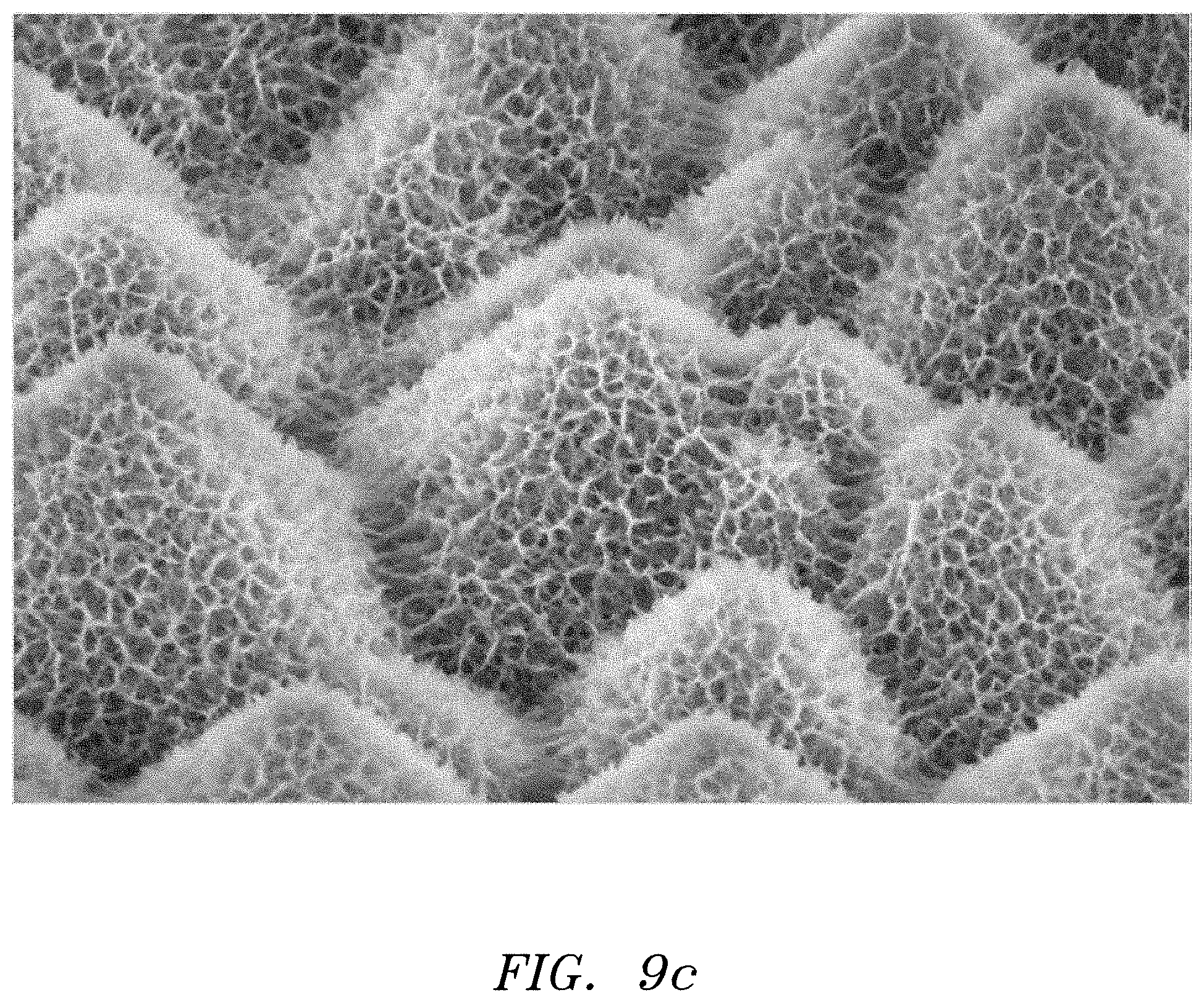
[0028] FIG. 9c is a microscopic image of a top view of an exemplary three-dimensional energy converter on a three-dimensional textured substrate as in FIG. 9a.
[0029] The above and other preferred features described herein, including various novel details of implementation and combination of elements, will now be more particularly described with reference to the accompanying drawings and pointed out in the claims. It will be understood that the particular methods and apparatuses are shown by way of illustration only and not as limitations of the claims. As will be understood by those skilled in the art, the principles and features of the teachings herein may be employed in various and numerous embodiments without departing from the scope of the claims.
DETAILED DESCRIPTION
[0030] A method and apparatus for converting chemical energy into electricity is described. Each of the features and teachings disclosed herein can be utilized separately or in conjunction with other features and teachings. Representative examples utilizing many of these additional features and teachings, both separately and in combination, are described in further detail with reference to the attached drawings. This detailed description is merely intended to teach a person of skill in the art further details for practicing preferred aspects of the present teachings and is not intended to limit the scope of the claims. Therefore, combinations of features disclosed in the following detailed description may not be necessary to practice the teachings in the broadest sense, and are instead taught merely to describe particularly representative examples of the present teachings.
[0031] In the following description, for purposes of explanation only, specific nomenclature is set forth to provide a thorough understanding of the various embodiments described herein. However, it will be apparent to one skilled in the art that these specific details are not required to practice the concepts described herein.
[0032] Moreover, the various features of the representative examples and the dependent claims may be combined in ways that are not specifically and explicitly enumerated in order to provide additional useful embodiments of the present teachings. It is also expressly noted that all value ranges or indications of groups of entities disclose every possible intermediate value or intermediate entity for the purpose of original disclosure, as well as for the purpose of restricting the claimed subject matter. It is also expressly noted that the dimensions and the shapes of the components shown in the figures are designed to help to understand how the present teachings are practiced, but not intended to limit the dimensions and the shapes shown in the examples.
[0033] Device structures and methods/processes described herein, for example, in FIGS. 4-9, include but are not limited to: (a) nanowires, nanofibers, or nanotubes; (b) porous nano-engineered structures with interconnecting walls and pores; and (c) porous nano-engineered structures with percolating networks. Fabrication methods/processes include but are not limited to direct film growth resulting in porous structures or/and nano-engineered structures. Methods of fabricating such devices include but are not limited to (i) stain oxidation and etching; (ii) dry and/or wet oxidation and etching; (iii) electrochemical oxidation and etching; (iv) anodization oxidation and etching; (v) micro-arc oxidation and etching; nano-particles of semiconductor(s), dielectric(s), metal(s), catalyst(s), metal salts in solvents, pastes, or colloids; and (vi) solgel processes. For certain semiconductors and dielectrics, e.g., silicon, only etching is required for all these fabrication methods/processes to introduce porosity and nano-engineered structures in the materials.
[0034] In certain embodiments, a chemical energy conversion device is described that utilizes porous semiconductor or dielectric and porous catalyst integrated one unit/network on a planar two-dimensional substrate or a three-dimensional substrate. A porous thin film of dielectric or semiconductor, such as a titanium dioxide (TiO.sub.2), which is sometimes referred to as titanium oxide, semiconducting network, can be fabricated by depositing a thin film of metallic titanium (Ti) on a non-porous planar substrate such as silicon, or on a non-porous supporting layer deposited on a planar substrate, such as a non-porous TiO.sub.2 layer on silicon. This deposited thin metallic Ti film can subsequently be oxidized to create TiO.sub.2 and further modified to form nano-porous holes in its microstructure through (i) stain oxidation and etching, (ii) dry or wet oxidation and etching, (iii) electrochemical oxidation and etching, (iv) anodization oxidation and etching, or (v) microarc oxidation and etching. Chemical reagents involved in all these processes include but are not limited to hydrofluoric acid (HF), nitric acid (HNO.sub.3), sulfuric acid (H.sub.2SO.sub.4), hydrogen peroxide (H.sub.2O.sub.2), or/and sodium hydroxide (NaOH). An additional non-porous layer of material functioning as a barrier layer can also be inserted between the deposited metallic Ti thin film and the planar substrate in order to further enhance device electrical performance. In another example the substrate itself can be a three-dimensional structure such as but not limited to porous silicon, textured silicon surfaces, and patterned silicon wafers. Likewise an additional non-porous thin layer of semiconductor or dielectric such as TiO.sub.2 may be inserted between the metallic Ti layer and the three-dimensional substrate described above.
[0035] Although the various embodiments disclosed herein are described as using TiO.sub.2, wherever TiO.sub.2, is discussed, other materials such as thin films of porous semiconductors and dielectrics with nano-engineered structures can be used without departing from the teachings herein. Such other thin-film porous materials include but are not limited to silicon; Al.sub.2O.sub.3; GaN; GaAs; Ge; silica; carbon; oxides of niobium, tantalum, zirconium, cerium, tin, and vanadium. These materials also apply to the underneath planar and three-dimensional substrates or supporting layers. The same processing methods can also be used in device fabrications.
[0036] As will be discussed, catalysts and/or conductors are placed on the internal and external surfaces of the porous semiconductor to create a plurality (and preferably, and large number) of solid state junctions. The catalysts and/or conductors that can be used to form the solid-state junctions with the porous nano-engineered semiconductor or dielectric network(s) can be noble metals such as but are not limited to Pt, Au, or Pd. These conductors and/or catalysts can be deposited using a number of methods, including but not limited to using nanoparticles or/and metal salts in solvents, pastes, or colloids; thin film deposition followed by annealing to nucleate the formation of nano-particles or a combination of pastes/solvent/deposition methods; chemical vapor deposition (CVD); sputtering; evaporation; atomic layer deposition (ALD); or solgel processes.
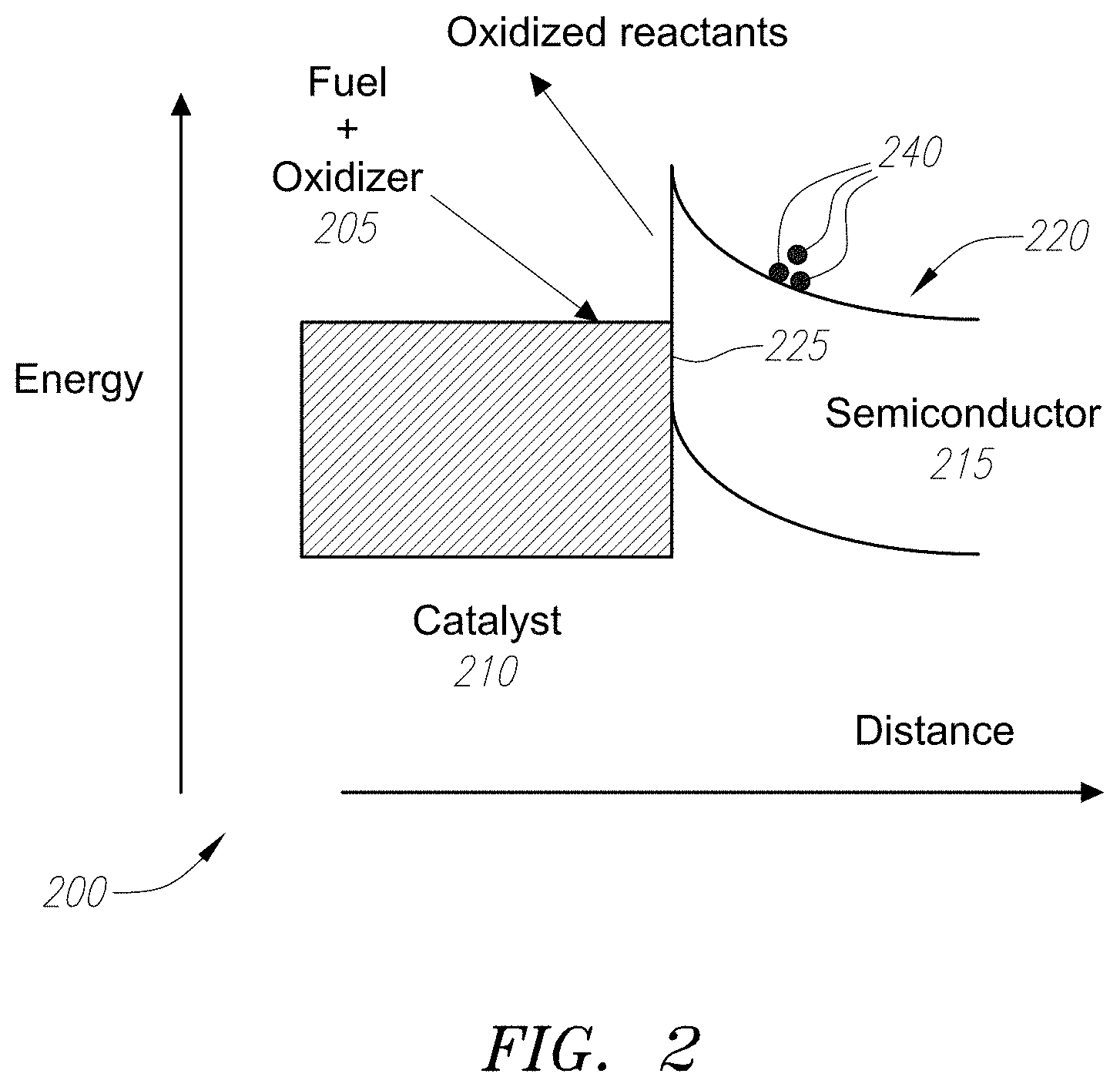
[0037] Turning to FIG. 2, a mechanism for energy conversion is described. FIG. 2 depicts an energy band diagram 200 for a catalyst-nanowire interface for an energy conversion device. Fuel plus oxidizer 205 comes into contact with the catalyst 210, which oxidizes upon contact. The oxidized fuel 210 injects electrons 240 into the conduction band 220 of the semiconductor 215. There, the electrons 240 encounter a Schottky-like potential barrier 225 between the semiconductor 215 and the catalyst 210, which may be a conductor, and may also be a top electrode layer (not shown) that embeds the catalyst. The electrons 240 are then directed towards the bottom contact (not shown) by the built-in electric field at the interface between the catalyst 210 and the semiconductor 215. The electrons 240 travel in the external circuit (not shown), thereby transferring their energy to the load before returning to the catalyst site via the top contact (also not shown). The electrons 240 then complete the reaction by reducing the oxidized reactants producing the final products. The output voltage of the circuit shown in FIG. 2 will depend on the potential offset (barrier) between the Fermi level in the catalyst and the conduction band of the semiconductor.
[0038] Alternatively, the semiconductor/catalyst surface may favor one of the oxidation or reduction reactions, effectively splitting the two reactions. This can create an electro-chemical potential gradient between the catalyst site and the semiconductor surface, which can induce an electro-motive force (EMF) in an external circuit and drive a load as shown in FIG. 3. In other words, as schematically shown in FIG. 3, the oxidation-reduction (redox) reactions induce an electron's chemical potential difference between the catalyst sites and the semiconductor sites, which in turn gives rise to an EMF (.DELTA..mu.=V.sub.2-V.sub.1).
[0039] The various embodiments described herein are chemical energy conversion devices that convert chemical energy to electricity. A limiting factor of prior devices using similar electron transport mechanisms as those described herein was the rate at which catalytic reactions could take place. Electricity generation of chemical energy converter devices like those described herein is proportional to the reaction rate and fuel conversion, and the reaction rate and fuel conversion are proportional to at least (i) the temperature at which the catalytic reactions take place, and (ii) the total surface areas of the catalyst. Increasing the surface area, however, generally leads to devices that become large two-dimensionally, and thus increases the size of the device, which is undesirable. Likewise, temperatures can be increased to enhance reaction rate, but increasing temperature can also be undesirable. The various embodiments described herein overcome these problems by increasing the surface area of the chemical energy converter device without significantly increasing the two-dimensional area of such devices.
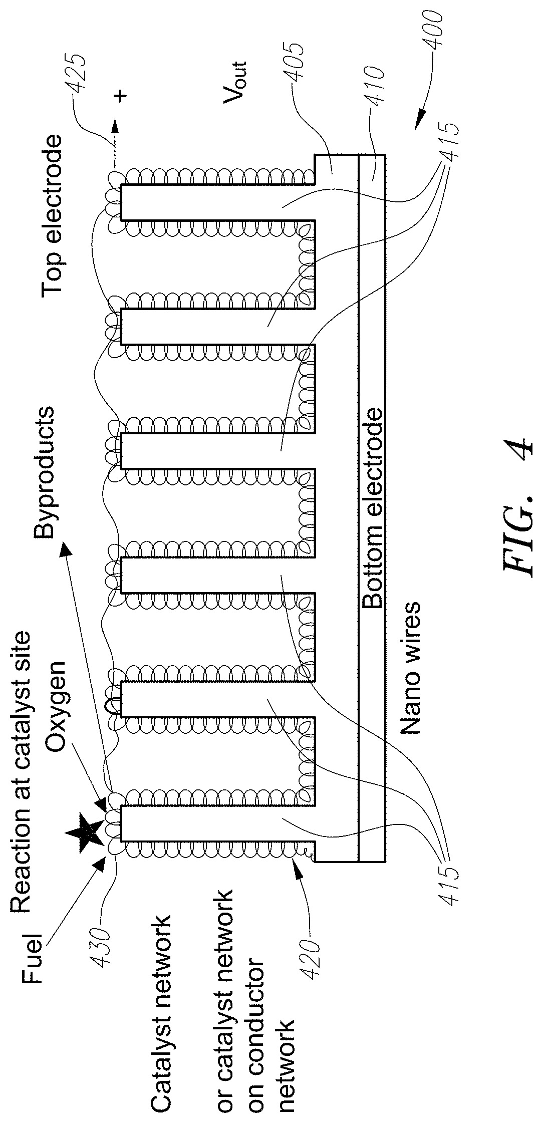
[0040] FIG. 4 illustrates an embodiment of a chemical energy converter device 400. In particular, FIG. 4 illustrates a device having nanowires 415, which are formed on a substrate layer (not shown), where the substrate layer can comprise a porous thin film of dielectric or semiconductor, such as a titanium oxide (TiO.sub.2). The substrate layer is formed on an electrode 410, which can be made with a metal conductive material or highly n-doped semiconductor material. Electrode 410 can be below the substrate layer or in-between the substrate and the nanowires 415. Nanowires 415 can comprise either a nano-engineered porous semiconductor material or a nano-engineered porous dielectric. Either way, nanowires 415 form an electrically conductive array. Catalyst material 420 is on the surface of the nanowire 415, although intervening materials are possible as well. The catalyst material 420 can be platinum particles, where each platinum particle forms a Schottky diode junction with the semiconductor material forming the nanowires 415. In use, fuel or energy source 430 such as hydrogen, or methanol or natural gas, and air, or a monopropellant energy source or fuel such as hydrogen peroxide comes in contact with the catalyst 420, which causes electrons from the catalyst 420 to be injected into the semiconductor 405, which are then attracted to the electrode 410. This generates electricity. A second electrode 425 is formed over the catalyst 420, which, in conjunction with the bottom electrode 410 allow a circuit to be formed so that electrical current will flow and a voltage potential V.sub.out is generated between the electrodes.
[0041] Nanowires 415 provide several advantages that improve the overall efficiency. The first advantage is increased surface area, which is provided by both the use of a porous substrate 405 and nanowires 415. Porous three-dimensional structures have a high surface to volume ratio when compared to non-porous two-dimensional planar layers. In addition, the nanowires 415 themselves have surface area, meaning that each nanowire 415 provides significantly more surface area than the same two-dimensional area would have provided were no nanowire 415 present. The additional surface area provided by the porous substrate 405 and the nanowires will have the ability to have more catalyst material disposed thereon, especially when compared to energy conversion devices that are two-dimensional. This is because presence of catalyst nano-particles, nano-clusters, or nano-wires on such a porous substrate provides more reaction sites for chemical reactions leading to increased reaction rates at lower temperatures. Another advantage is that porous network also facilitates diffusion of reactants to catalysts located on the internal surfaces of the nanowires and removal of reaction products away from the catalysts.
[0042] In an embodiment, nanowires 415 are comprised of single crystal TiO.sub.2 nanowires, which enhance electron transport, can be synthesized in various simple inexpensive methods, such as growth from an epitaxial seed layer from a titanium source e.g. in a hydrothermal process. The bottom contact 410 is a conductive substrate with a conductive layer that provides an epitaxial template for nanowire growth, e.g. FTO (fluorinated tin oxide) in the case of TiO.sub.2 nanowires. The top contact 425 has to electrically connect the porous network of the catalyst. The catalyst can be a paste or an electrolyte. Again, the conductor and or catalysts can be deposited used nano-particle pastes, nano-particle solvents, thin film depositions or any combinations thereof.
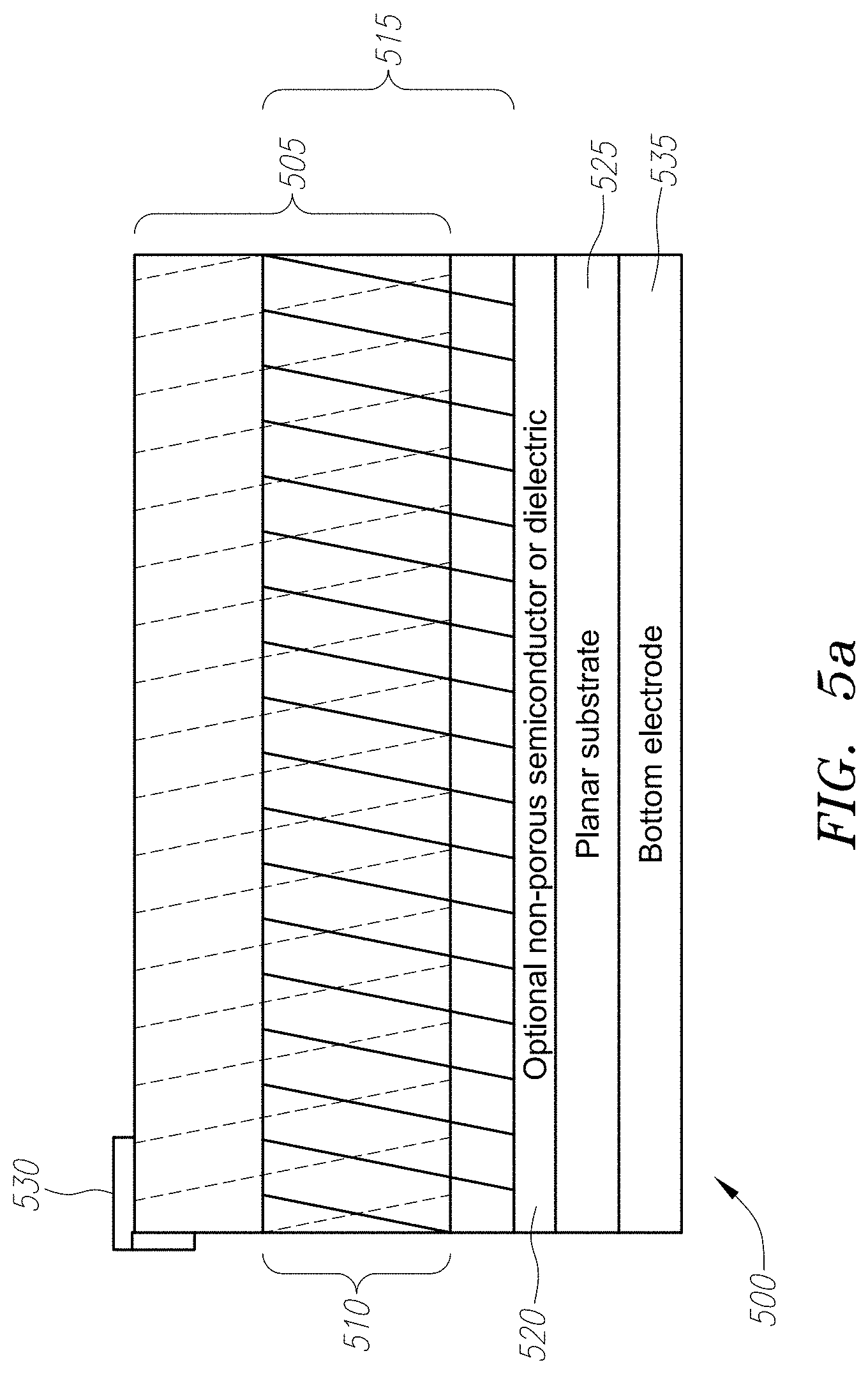
[0043] FIG. 5a illustrates another embodiment of an energy converter device comprising a three-dimensional porous catalyst layer 505 intertwined three-dimensionally with porous semiconductor or dielectric layer 515 at an intertwining region 510, which in turn can be placed on a planar substrate 525. Layer 515 can be constructed with TiO.sub.2 as discussed above, and can take the form of a honeycomb-like structure being either a nano-engineered structure having interconnecting walls defining pores, or nano-engineered structures with percolating networks. Either way, the honeycomb-like structure allows catalyst nano-particles from the catalyst layer to enter the spaces of the honeycomb structure and rest on the surface of the semiconductor or dielectric layer 515. It is this honeycomb structure that makes layer 515 porous in three dimensions. These nano-particles can, for example, be platinum. The honeycomb-like structure of the semiconductor or dielectric layer 515 can be seen in the photographs of FIGS. 5b-5c.
[0044] Likewise, the three-dimensional porous catalyst layer 505 can comprise porous networks, individual nano-clusters/particles, or a combination of both, and can be constructed from, for example, platinum. As with porous semiconductor or dielectric layer 515, catalyst layer can take the form of a honeycomb-like structure. An exemplary three-dimensional porous layer 505 can be seen in the photographs of FIGS. 5b-5c. A feature of the intertwining region 510 is its large internal surface area where catalysts can be distributed throughout to construct a three-dimensional network of catalyst-semiconductor junctions. An exemplary intertwining region 510 can be seen in the photographs of FIGS. 5b-5c.
[0045] Chemical energy converter 500 can optionally include a non-porous semiconductor or dielectric layer 520 deposited through standard deposition methods such as evaporation, chemical vapor deposition (CVD), sputtering, or atomic layer deposition (ALD), to provide a barrier layer between the substrate below and the porous materials above.
[0046] In the embodiment illustrated by FIG. 5, a top electrode 530 can be formed on part or all of catalyst layer 505. Likewise, a bottom electrode 535 can be formed underneath planar substrate 520. These two electrodes can be electrically connected to an external load to form a complete circuit.
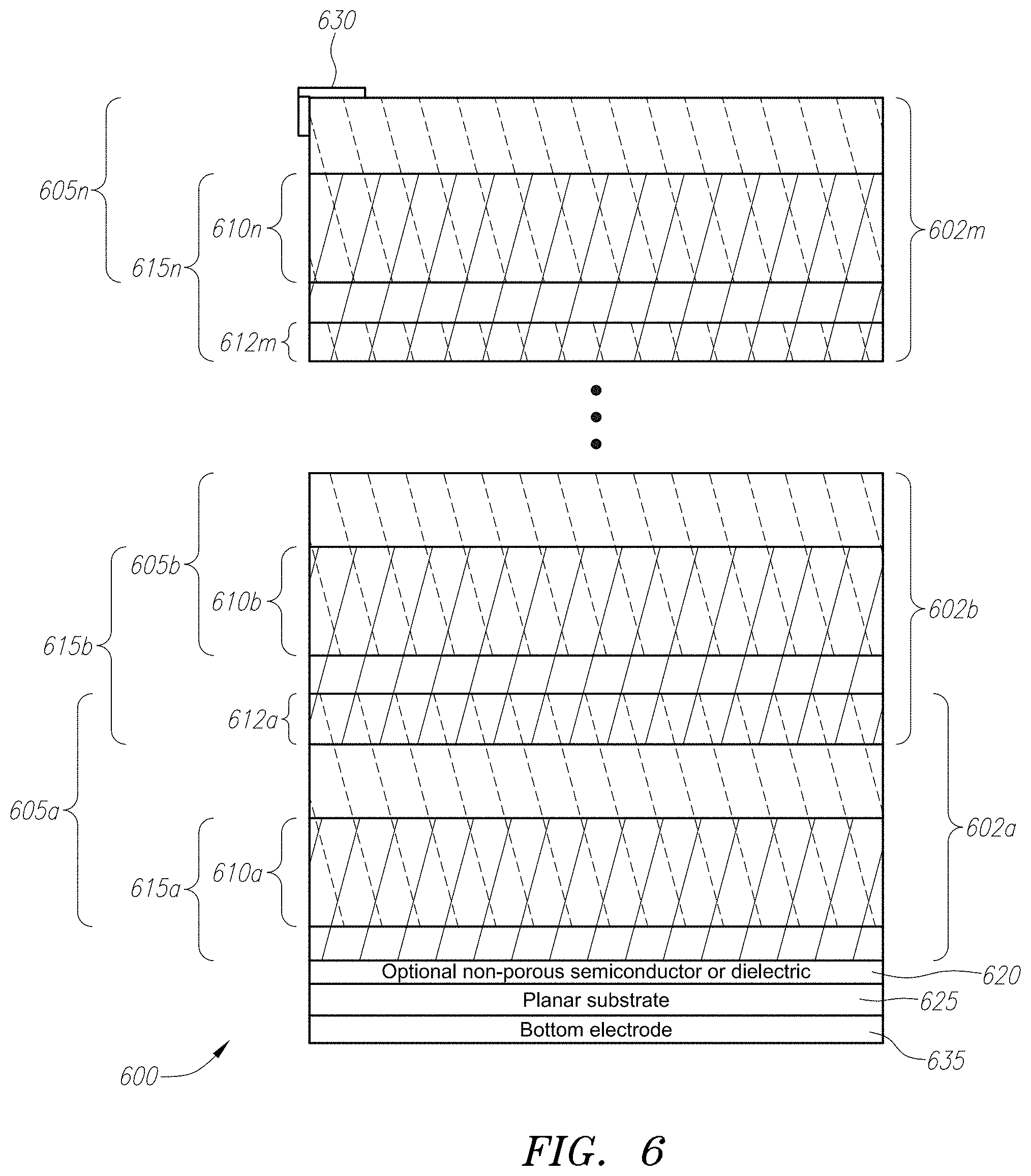
[0047] FIG. 6 shows yet another embodiment, where a plurality of chemical energy converter devices 500 as in FIG. 5(a) are arranged as n cells 602a-602n and are thus stacked on top of each other. A chemical energy converter 600 as shown in FIG. 6 is a multi-cell device structure with multiple layers of porous catalyst 605a-605n and porous semiconductor/dielectric networks 615a-615n that can be fabricated and integrated vertically on a planar two-dimensional substrate. In particular, chemical energy converter 600 can have a bottom electrode 635, which has a planar substrate 625 disposed thereon. A non-porous semiconductor or dielectric layer 620 can, if desired, be placed on the planar substrate 625. Use of such a layer 620 acts as a barrier layer between substrate below and the porous materials above. The first cell 602a of the chemical energy converter 600 comprises a porous layer 615a comprised of a semiconductor or dielectric material, which can be constructed, for example, from TiO.sub.2. The first cell 602a also comprises a three-dimensional porous catalyst layer 605a that is placed thereon using methods described above, and can comprise porous networks, individual nano-clusters/particles, or a combination of both. Catalyst layer 605a can be constructed from, for example, platinum. At the interface between layer 615a and catalyst layer 605a, the materials intertwine three-dimensionally in a first intertwined region 610a.
[0048] To increase the amount of energy generated, chemical energy converter device 600 has additional cells 602b through 602n stacked on top of each other. For example, a second cell 602b comprised of second porous layer 615b and second catalyst layer 605b are formed above the first cell, with a three-dimensional intertwined region 612a formed between the first cell 602a and second cell 602b. Likewise a third three-dimensional intertwined region 610b is formed between the second catalyst layer 605b and second porous semiconductor or dielectric layer 615b.
[0049] To further increase energy generation, n additional cells 602n can be added to chemical energy converter 600. Each of the additional cells is comprised of n second catalyst layers 605n and n porous semiconductor or dielectric layers 615n, with a three-dimensional intertwined region 610n formed at every interface between catalyst layers 605n and porous semiconductor or dielectric layer 615n. A three-dimensional intertwined region 612a-612m will be formed between each cell. Such multi-cell structures significantly increase the total catalyst-semiconductor interfacial area without including a larger device, thereby increasing fuel conversion via chemical reactions and corresponding electrical output.
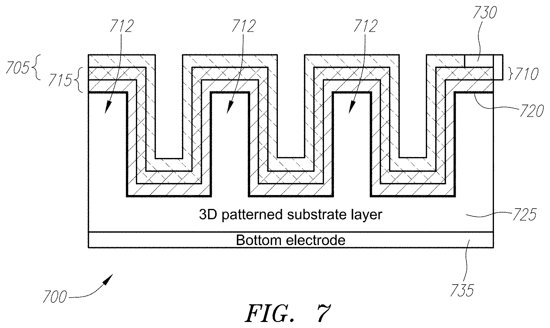
[0050] Yet another embodiment illustrated in FIG. 7, in which a chemical energy converter 700 has the integration of porous catalyst and porous semiconductor described in FIG. 5 constructed on a three-dimensional surface. Such a three-dimensional surface has surface area larger than a planar two-dimensional substrate, which results in increased fuel conversion and reaction rates, which in turn increases the amount of electricity generated. In particular, the embodiment described with reference to FIG. 7 has a bottom electrode 735. A three-dimensional substrate 725 is fabricated thereon using, for example, a standard lithography patterning/etching process. In this embodiment substrate 725 forms a patterned three-dimensional network micro-trenches 712. If desired, a non-porous layer 720 can be placed over the patterned substrate 725, which acts as a barrier layer between the substrate below and the porous materials above. As in the embodiment shown in FIG. 5, a porous semiconductor/dielectric network 715 is placed over patterned substrate 725 (or non-porous layer 720, if present). A catalyst layer 705 is placed over the porous semiconductor/dielectric network 715, which also enters the pores of the porous semiconductor/dielectric network 715 to form an intertwining region 710. A second electrode 730 is placed above a catalyst layer 705, and in combination with first electrode 735, allows a voltage to appear, and hence allows for the use of the electricity generated by the converter device 700.
[0051] FIG. 8 shows an embodiment of a chemical energy converter 800 comprising a porous three-dimensional substrate/supporting layer 825 where internal and external surfaces are covered with the integration of a porous semiconductor or dielectric layer 815 and a porous catalyst 805 similar to that described in FIG. 5. In particular, chemical energy converter device 800 has a bottom electrode 835, upon which a porous substrate/supporting layer 825 is placed thereon.
[0052] A second electrode 830 is placed above layer 825, and in combination with first electrode 835, allows a voltage to appear, and hence allows for the use of the electricity generated by the converter device 800.
[0053] Three-dimensional porous substrate is typically amorphous, which, upon annealing can crystallize. Nano-engineered structures typically consist of interconnected walls and wires forming a highly porous structure. The size of the pores, the thickness of the porous layer, among other physical and electrical properties, can be tuned by the processing parameters.
[0054] Another method to create a nano-engineered porous network or layer of semiconductor or dielectric, for example TiO.sub.2, as a support to the catalyst above it, is to utilize a paste of TiO.sub.2 nano-particles to form thin films of porous layers/networks.
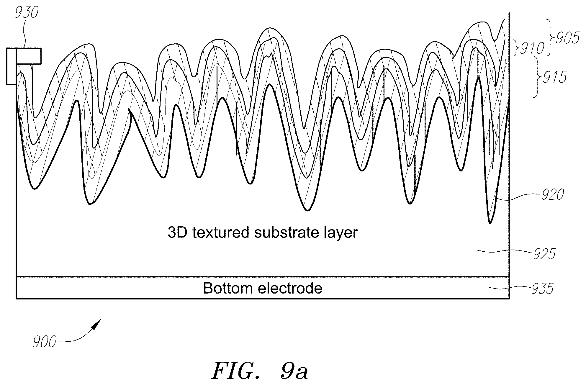
[0055] FIG. 9a shows an embodiment having a three-dimensional textured substrate/supporting layer 925 where the surface is covered with the integration of porous semiconductor or dielectric material layer 915 and porous catalyst 905 like the embodiment described in FIG. 5. In particular, the chemical energy converter 900 illustrated in FIG. 9 has a bottom electrode 935. Placed thereon is a three-dimensional textured substrate 925, which for example can be created by etching a silicon wafer.
[0056] Textured substrate 925 forms peaks and valleys, thereby creating a three-dimensional reaction area. This three-dimensional reaction area increases the surface area available for chemical reactions, which increases the number of reactive sites that can take place during a particular amount of time for a given device size, thereby increasing the electrical generation capability of the energy converter 900. If desired, a non-porous layer 920 can be placed over the textured substrate 905. As above, the non-porous layer 920 provides a barrier layer to separate the substrate below and the porous materials above. A porous or semiconductor or dielectric layer 915 is placed over the textured substrate 925 (or non-porous layer, if present).
[0057] A catalyst layer 905 is placed over the porous semiconductor/dielectric network 915, which also enters the pores of the porous semiconductor/dielectric network 915 to form an intertwining region 910. A second electrode 930 is placed above a catalyst layer 905, and in combination with first electrode 935, allows a voltage to appear, and hence allows for the use of the electricity generated by the converter device 900.
[0058] As in the other embodiments described herein, the use of a textured substrate 905 results in an increased surface area for catalysis, which results in greater electricity generation than an energy converter having a planar two-dimensional substrate.
[0059] FIG. 9b is a photograph depicting an energy converter as in FIG. 9a having a textured substrate. The photograph shows substrate 925 having a semiconductor or dielectric layer 915 formed thereon. Catalyst layer 905 in the form of nano-particles is over the dielectric/semiconductor layer 915, and nano-particles enter the pores of layer 915 to form an intertwining region. FIG. 9c shows a planar view, where one can see the texture of the dielectric/semiconductor layer 915.
[0060] Device structures, and methods/processes to fabricate them, using nanowire arrays, nano-engineered structures, to form porous networks comprising solid-state junctions specifically to convert chemical into electrical energy are described herein. The device structures can be fabricated on a two-dimensional planar substrate or on a three-dimensional substrate. An exemplary method comprises fabricating one or more solid-state electric generators. The solid-state electric generators include one or more chosen from the group including a chemically energized solid-state electric generator. A solid state electric generator energizes charge carriers in a first material forming a junction with a second material. The second material has a finite energy gap with a conduction band that has an offset with the Fermi level of the first material.
[0061] The present methods, devices and systems improve the energy conversion efficiency of junctions used in solid-state devices to generate electricity. An energy source injects charge carriers, e.g. electrons, on one side of a junction. When a net excess of charge carriers is injected from one side of a junction to the other, it will be forced to travel in the external circuit by the electric field. The result is the conversion of chemical energy into the useful form of an electrical energy. An element of the embodiments is that the efficiency of this process is improved when the charge transport or mobility is improved in the semiconducting material.
[0062] An alternative mechanism for generating power is creating an electrochemical potential difference between the nanowire network or nano-engineered porous networks/layers and the catalyst which can act as an electromotive force (EMF). The semiconductor/catalyst surface may favor one of the oxidation or reduction reactions, effectively splitting the two reactions. This can create an electro-chemical potential gradient between the catalyst site and the semiconductor surface which can induce an electro-motive force (EMF) in an external circuit and drive a load.
[0063] One embodiment includes nanowire array or nano-engineered porous networks/layers made from dielectric or semiconductor including but not limited to, for example, rutile TiO2, anatase TiO2, poly-crystalline TiO.sub.2 porous TiO2, ZrO2, SrTiO.sub.3, BaTiO3, Sr_x-Ba_y-TiO_z, LiNiO, silicon, SiC; GaN; GaAs; Ge; silica; carbon; oxides of niobium, tantalum, zirconium, cerium, tin, vanadium, and LaSrVO.sub.3, and certain organic semiconductors, such as PTCDA, or 3,4,9,10-perylenetetracarboxylicacid-dianhydride. The subscripts x, y and z denote concentrations, per usual conventions. One advantage of SrTiO.sub.3 is that Schottky barriers on it may be unpinned, providing a relatively larger barrier compared to that of TiO.sub.2.
Fuels, Oxidizers, Autocatalysts, Stimulators
[0064] The various chemical energy converter devices described herein use storable reactants including oxidizers, autocatalytic reaction accelerators, decelerators, and monopropellants. The liquid phase, such as liquid hydrogen peroxide H.sub.2O.sub.2 at standard pressure and temperature, are convenient because their heat of vaporization is used as coolant and the liquid is conveniently storable. Monopropellants such as H.sub.2O.sub.2 and monomethylhydrazine (MMH) are similarly convenient and energize the active surface of converters. Autocatalytic accelerators include monopropellants such as H.sub.2O.sub.2.
[0065] One embodiment uses reactions and reactants to energize these excitations. The reactions, reactants and additives include at least monopropellants, high energy fuels with oxidizers, hypergolic mixtures, and additives and combinations of reactants known to produce autocatalytic specie, reactants chosen to accelerate reactions or to control reactions, and combinations thereof. The reactants and/or additives include but are not limited to the following reactants:
Energetic Fuels More Storable than Ammonia: [0066] amine substituted ammonias [0067] Di-Methyl-Amine (CH.sub.3).sub.2NH [0068] Tri-Methyl-Amine (CH.sub.3).sub.3N [0069] Mono-Ethyl-Amine (C2H5)NH2 [0070] Di-Ethyl-Amine (C.sub.2H.sub.5).sub.2NH)
Other Classes More Easily Storable:
[0070] [0071] Methanol, CH.sub.3OH [0072] Ethanol, EtOH CH3CH2OH [0073] Formic Acid, HCOOH [0074] diesel fuels [0075] gasoline [0076] alcohols [0077] slurries including solid fuels [0078] Carbon Suboxide, C.sub.3O.sub.2, CO.dbd.C.dbd.CO, [0079] Formaldehyde HCHO, [0080] Paraformaldehyde,=better HCHO).sub.n, sublimeable to Formaldehyde gas. (Potentially a cell coolant at the same time).
Less Storable Fuels:
[0080] [0081] Carbon Monoxide [0082] Hydrogen [0083] Ammonia NH3
Energetic Fuels Containing Nitrogen:
[0083] [0084] Nitromethane, CH.sub.3NO.sub.2 [0085] Nitromethane "cut" with Methanol=model airplane "glow plug" engine fuel High Energy Fuels with Wide Fuel/Air Ratio: [0086] Epoxy-Ethane, =Oxirane or Ethylene-Oxide CH2-CH2 O [0087] 1,three-Epoxy-Propane=Oxetane and Tri-Methylene-Oxide=1,three-Methylene-Oxide CH.sub.2--(CH.sub.2)--CH.sub.2 O [0088] Epoxy-Propane CH2-(CH2)-CH2 O [0089] Acetylene, C.sub.2H.sub.2 [0090] Diacetylene=1,three-Butadiyne [0091] 1,three-Butadiene CH.sub.2.dbd.CH--CH.dbd.CH.sub.2,
Less Exotic High Energy Fuels:
[0091] [0092] Di-Ethyl-Ether or surgical ether [0093] Acetone=Di-Methyl-Ketone
Less Exotic, Volatile Fuels:
[0093] [0094] Cyclo-Propane [0095] Cyclo-Butane [0096] Hydrocarbons such as methane, propane, butane, pentane, etc.
Other Storable Fuels:
[0096] [0097] Methyl Formate HCOO--C.sub.2H.sub.5 [0098] Formamide HCO--NH2 [0099] N, N,-Di-Methyl-Formamide HCO--N--(CH.sub.3).sub.2 [0100] Ethylene-Diamine H.sub.2N--CH.sub.2--CH.sub.2--NH.sub.2 [0101] Ethylene-Glycol [0102] 1,4-Dioxane=bimolecular cyclic ether of Ethylene-Glycol [0103] Paraldehyde (CH.sub.3CHO).sub.3 cyclic trimer of Acetaldehyde
Powerful Oxidizer:
[0103] [0104] Tetra-Nitro-Methane, C(NO.sub.2).sub.4 . . . does not spontaneously decompose . . . just pass the two separate vapors over the reaction surface of the cell in the gas phase [0105] Hydrogen Peroxide H2O2
Low Initiation Energy Mixtures:
[0105] [0106] Cyclo-Propane with Oxygen=surgical anesthetic, microjoules initiator
Hypergolics:
[0106] [0107] UDMH=Unsymmetrical DiMethyl Hydrazine=1,1-DiMethyl Hydrazine (CH.sub.3).sub.2NNH.sub.2 [0108] UDMH is hypergolic usually with N.sub.2O.sub.4 and is a very potent carcinogen [0109] MMH MonoMethyl Hydrazine (CH.sub.3)HNNH.sub.2 hypergolic with any oxidizers, e.g. N.sub.2O.sub.4
Corrosive Toxic Energetic Monopropellant:
[0109] [0110] Hydrazine=H.sub.2NNH.sub.2 decomposed easily with a catalyst (usually Pt or Pd or Molybdenum Oxide [0111] Hydrazine Hydrate
[0112] Although various embodiments have been described with respect to specific examples and subsystems, it will be apparent to those of ordinary skill in the art that the concepts disclosed herein are not limited to these specific examples or subsystems but extends to other embodiments as well. Included within the scope of these concepts are all of these other embodiments as specified in the claims that follow.
* * * * *
D00000
D00001
D00002
D00003
D00004
D00005
D00006
D00007
D00008
D00009
D00010
D00011
D00012
XML
uspto.report is an independent third-party trademark research tool that is not affiliated, endorsed, or sponsored by the United States Patent and Trademark Office (USPTO) or any other governmental organization. The information provided by uspto.report is based on publicly available data at the time of writing and is intended for informational purposes only.
While we strive to provide accurate and up-to-date information, we do not guarantee the accuracy, completeness, reliability, or suitability of the information displayed on this site. The use of this site is at your own risk. Any reliance you place on such information is therefore strictly at your own risk.
All official trademark data, including owner information, should be verified by visiting the official USPTO website at www.uspto.gov. This site is not intended to replace professional legal advice and should not be used as a substitute for consulting with a legal professional who is knowledgeable about trademark law.