Low Insertion Loss RF Transmission Line
Popovich; Mark ; et al.
U.S. patent application number 16/631700 was filed with the patent office on 2020-05-28 for low insertion loss rf transmission line. The applicant listed for this patent is 3D GLASS SOLUTIONS, INC.. Invention is credited to Jeff A. Bullington, Jeb H. Flemming, Mark Popovich.
| Application Number | 20200168976 16/631700 |
| Document ID | / |
| Family ID | 68698438 |
| Filed Date | 2020-05-28 |


| United States Patent Application | 20200168976 |
| Kind Code | A1 |
| Popovich; Mark ; et al. | May 28, 2020 |
Low Insertion Loss RF Transmission Line
Abstract
The present invention includes a method of creating electrical air gap or other low loss low cost RF mechanically and thermally stabilized interdigitated resonate filter in photo definable glass ceramic substrate. A ground plane may be used to adjacent to or below the RF filter in order to prevent parasitic electronic signals, RF signals, differential voltage build up and floating grounds from disrupting and degrading the performance of isolated electronic devices by the fabrication of electrical isolation and ground plane structures on a photo-definable glass substrate.
| Inventors: | Popovich; Mark; (Coto de Caza, CA) ; Flemming; Jeb H.; (Albuquerque, NM) ; Bullington; Jeff A.; (Orlando, FL) | ||||||||||
| Applicant: |
|
||||||||||
|---|---|---|---|---|---|---|---|---|---|---|---|
| Family ID: | 68698438 | ||||||||||
| Appl. No.: | 16/631700 | ||||||||||
| Filed: | May 29, 2019 | ||||||||||
| PCT Filed: | May 29, 2019 | ||||||||||
| PCT NO: | PCT/US2019/034245 | ||||||||||
| 371 Date: | January 16, 2020 |
Related U.S. Patent Documents
| Application Number | Filing Date | Patent Number | ||
|---|---|---|---|---|
| 62677537 | May 29, 2018 | |||
| Current U.S. Class: | 1/1 |
| Current CPC Class: | C03C 3/095 20130101; C03C 17/06 20130101; H01Q 1/38 20130101; C03C 10/0009 20130101; H03H 7/38 20130101; C03C 4/04 20130101; C03C 2214/08 20130101; H01P 11/001 20130101; H03H 2007/013 20130101; C03C 23/0005 20130101; H01P 3/003 20130101; H01Q 9/0407 20130101; C03C 14/004 20130101; H03H 7/0161 20130101; C03C 15/00 20130101 |
| International Class: | H01P 11/00 20060101 H01P011/00; H01P 3/00 20060101 H01P003/00; C03C 17/06 20060101 C03C017/06; H01Q 9/04 20060101 H01Q009/04; C03C 23/00 20060101 C03C023/00; H03H 7/38 20060101 H03H007/38; C03C 4/04 20060101 C03C004/04; H03H 7/01 20060101 H03H007/01 |
Claims
1. A method of making a mechanically stabilized RF transmission line device comprising: masking a design layout comprising one or more structures that form one or more transmission line structures on a photosensitive glass substrate; exposing at least one portion of the photosensitive glass substrate to an activating energy source; heating the photosensitive glass substrate for at least ten minutes above its glass transition temperature; cooling the photosensitive glass substrate to transform at least part of the exposed glass into a glass-crystalline substrate; etching the glass-crystalline substrate with an etchant solution to form one or more trenches and a mechanical support under the design layout of the one or more transmission line structures with electrical conduction channels; and printing or depositing one or more metals or metallic media that form the one or more electrical conductive transmission lines, a ground plane and one or more input and output channels, wherein the metal is connected to a circuitry that forms the RF transmission line device, and at least one of the electrical conductive transmission lines is mechanically supported by the mechanical support.
2. The method of claim 1, wherein the device is covered with a coating or lid that covers all or part of at least one of: the electrical conductive transmission lines, ground plane and input and output channels with the metal or metallic media further comprises connecting the metal or metallic media to a ground.
3. The method of claim 1, wherein the mechanical support is a low loss tangent mechanical and thermal stabilization structure under the one or more electrical conductive transmission lines that is less than or equal to 100% of the contact area of the one or more electrical conductive transmission lines.
4. The method of claim 1, wherein the mechanical support is a low loss tangent mechanical support under less than 50% of the contact area of the one or more electrical conductive transmission lines.
5. The method of claim 1, wherein the mechanical support is a low loss tangent mechanical support under less than 10% of the contact area of the one or more electrical conductive transmission lines.
6. The method of claim 1, wherein the mechanical support is a low loss tangent mechanical support under less than 1% of the contact area of the one or more electrical conductive transmission lines.
7. The method of claim 1, wherein the mechanical support forms a support pedestal with an integrated ceramic core with glass cladding.
8. The method of claim 7, wherein the support pedestal has a glass cladding that is less than 40% of the volume of the pedestal.
9. The method of claim 7, wherein the support pedestal has a glass cladding that is less than 20% of the volume of the support pedestal.
10. The method of claim 7, wherein the support pedestal has a glass cladding that is less than 10% of the volume of the support pedestal.
11. The method of claim 7, wherein the support pedestal has a glass cladding that is less than 5% of the volume of the support pedestal.
12. The method of claim 1, wherein the mechanically stabilized RF transmission line device is a bandpass, shunt low pass, high pass, or notch.
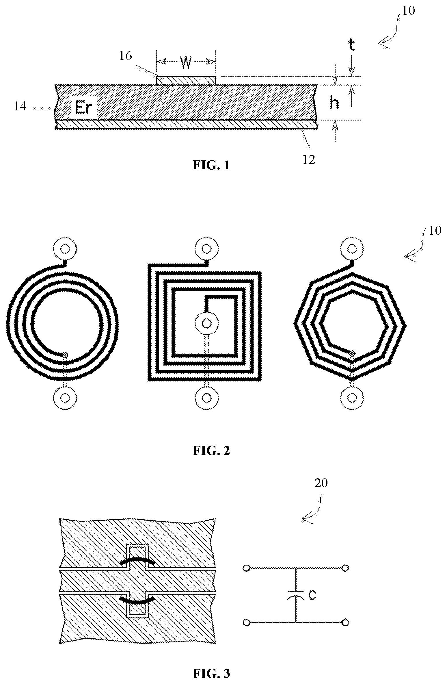
13. The method of claim 8, wherein a metal or metal media comprised at least one of: titanium, titanium-tungsten, chrome, copper, nickel, gold, palladium or silver.
14. The method of claim 1, wherein the step of etching forms an air gap between the substrate and the one or more electrical conductive transmission lines, wherein the structure is connected to one or more RF electronic elements.
15. The method of claim 1, wherein the glass-crystalline substrate adjacent to the trenches is converted to a ceramic phase.
16. The method of claim 1, wherein the metal is connected to the circuitry through a surface, a buried contact, a blind via, a glass via, a straight-line contact, a rectangular contact, a polygonal contact, or a circular contact.
17. The method of claim 1, wherein the photosensitive glass substrate is a glass substrate comprising a composition of: 60-76 weight % silica; at least 3 weight % K.sub.2O with 6 weight %-16 weight % of a combination of K.sub.2O and Na.sub.2O; 0.003-1 weight % of at least one oxide selected from the group consisting of Ag.sub.2O and Au.sub.2O; 0.003-2 weight % Cu.sub.2O; 0.75 weight %-7 weight % B.sub.2O.sub.3, and 6-7 weight % Al.sub.2O.sub.3; with the combination of B.sub.2O.sub.3; and Al.sub.2O.sub.3 not exceeding 13 weight %; 8-15 weight % Li.sub.2O; and 0.001-0.1 weight % CeO.sub.2.
18. The method of claim 1, wherein the photosensitive glass substrate is a glass substrate comprising a composition of: 35-76 weight % silica, 3-16 weight % K.sub.2O, 0.003-1 weight % Ag.sub.2O, 8-15 weight % Li.sub.2O, and 0.001-0.1 weight % CeO.sub.2.
19. The method of claim 1, wherein the photosensitive glass substrate is at least one of: a photo-definable glass substrate comprises at least 0.1 weight % Sb.sub.2O.sub.3 or As.sub.2O.sub.3; a photo-definable glass substrate comprises 0.003-1 weight % Au.sub.2O; a photo-definable glass substrate comprises 1-18 weight % of an oxide selected from the group consisting of CaO, ZnO, PbO, MgO, SrO and BaO; and optionally has an anisotropic-etch ratio of exposed portion to said unexposed portion is at least one of 10-20:1; 21-29:1; 30-45:1; 20-40:1; 41-45:1; and 30-50:1.
20. The method of claim 1, wherein the photosensitive glass substrate is a photosensitive glass ceramic composite substrate comprising at least one of silica, lithium oxide, aluminum oxide, or cerium oxide.
21. The method of claim 1, wherein the RF transmission line device has a loss of less than 50, 40, 30, 25, 20, 15, or 10% of the signal input versus a signal output.
22. The method of claim 1, wherein the RF transmission line device has a loss of less than 0.4 dB/cm at 30 Ghz.
23. The method of claim 1, further comprising forming one or more RF mechanically and thermally stabilized interdigitated resonate structures using the method into a feature of at least one of a patch antenna, transmission line, delay line, bandpass, low pass, high pass, or notch filter.
24. The device of claim 20, wherein the RF transmission line has mechanical support under less than 10% of the contact area of the RF interdigitated resonate structure.
25. The device of claim 20, wherein the RF transmission line device has mechanical and thermal stabilization structure is under less than 5% of the contact area.
26. The device of claim 20, wherein the RF transmission line device is an RF filter line that has the mechanical and thermal stabilization structure under less than 1% of the contact area of the one or more electrical conductive transmission lines.
27. A method of making a mechanically stabilized RF transmission line device comprising: masking a design layout comprising one or more structures that form one or more transmission line structures with electrical conduction channels on a photosensitive glass substrate; exposing at least one portion of the photosensitive glass substrate to an activating energy source; heating the photosensitive glass substrate for at least ten minutes above its glass transition temperature; cooling the photosensitive glass substrate to transform at least part of the exposed glass to a crystalline material to form a glass-crystalline substrate; etching the glass-crystalline substrate with an etchant solution to form a mechanical support device; and coating the one or more electrical conductive interdigitated transmission lines, ground plane and input and output channels with one or more metals, wherein the metal is connected to a circuitry.
28. The method of claim 27, further comprising forming one or more RF mechanically and thermally stabilized interdigitated resonate structures using the method into a feature of at least one of a patch antenna, transmission line, delay line, bandpass, low pass, high pass, or notch filter.
29. (canceled)
30. (canceled)
Description
CROSS-REFERENCE TO RELATED APPLICATIONS
[0001] None.
STATEMENT OF FEDERALLY FUNDED RESEARCH
[0002] None.
TECHNICAL FIELD OF THE INVENTION
[0003] The present invention relates to creating impedance matching between RF devices on the same substrate. Low Insertion Loss Transmission Line with a ceramic/glass support pedestal that has up to 100% contact/support of a transmission line and affiliated devices (filters).
BACKGROUND OF THE INVENTION
[0004] Without limiting the scope of the invention, its background is described in connection with impedance matching.
[0005] One such example is taught in U.S. Pat. No. 9,819,991, issued to Rajagopalan, et al., entitled "Adaptive impedance matching interface". These inventors are said to teach a device, that includes a data interface connector, an application processor, and interface circuitry. Interface circuitry is said to be coupled between the application processor and the data interface connector, in which the data interface circuitry determines a change in a signal property of one of the signals, the change being caused by an impedance mismatch between the data interface connector and a media consumption device. The application processor is said to adjust the signal property of a subsequent one of the signals, in response to the signal property setting from the interface circuitry, to obtain an adjusted signal, or can send the adjusted signal to the media consumption device.
[0006] Another such example is taught in U.S. Pat. No. 9,755,305, issued to Desclos, et al., and entitled "Active antenna adapted for impedance matching and band switching using a shared component". Briefly, these inventors are said to teach an active antenna and associated circuit topology that is adapted to provide active impedance matching and band switching of the antenna using a shared tunable component, e.g., using a shared tunable component, such as a tunable capacitor or other tunable component. The antenna is said to provide a low cost and effective active antenna solution, e.g., one or more passive components can be further utilized to design band switching of the antenna from a first frequency to a second desired frequency.
[0007] However, despite these advances, a need remains compact low loss RF transmission line and affiliated devices (filters).
SUMMARY OF THE INVENTION
[0008] In one embodiment, the present invention includes a method of making a mechanically stabilized RF transmission line device comprising: masking a design layout comprising one or more structures that form one or more transmission line structures on a photosensitive glass substrate; exposing at least one portion of the photosensitive glass substrate to an activating energy source; heating the photosensitive glass substrate for at least ten minutes above its glass transition temperature; cooling the photosensitive glass substrate to transform at least part of the exposed glass into a glass-crystalline substrate; etching the glass-crystalline substrate with an etchant solution to form one or more trenches and a mechanical support under the design layout of the one or more transmission line structures with electrical conduction channels; and printing or depositing one or more metals or metallic media that form the one or more electrical conductive transmission lines, a ground plane and one or more input and output channels, wherein the metal is connected to a circuitry that forms the RF transmission line device, and at least one of the electrical conductive transmission lines is mechanically supported by the mechanical support. In one aspect, the device is covered with a coating or lid that covers all or part of at least one of: the electrical conductive transmission lines, ground plane and input and output channels with the metal or metallic media further comprises connecting the metal or metallic media to a ground. In another aspect, the mechanical support is a low loss tangent mechanical and thermal stabilization structure under the one or more electrical conductive transmission lines that is less than or equal to 100% of the contact area of the one or more electrical conductive transmission lines. In another aspect, the mechanical support is a low loss tangent mechanical support under less than 50% of the contact area of the one or more electrical conductive transmission lines. In another aspect, the mechanical support is a low loss tangent mechanical support under less than 10% of the contact area of the one or more electrical conductive transmission lines. In another aspect, the mechanical support is a low loss tangent mechanical support under less than 1% of the contact area of the one or more electrical conductive transmission lines. In another aspect, the mechanical support forms a support pedestal with an integrated ceramic core with glass cladding. In another aspect, the support pedestal has a glass cladding that is less than 40% of the volume of the pedestal. In another aspect, the support pedestal has a glass cladding that is less than 20% of the volume of the support pedestal. In another aspect, the support pedestal has a glass cladding that is less than 10% of the volume of the support pedestal. In another aspect, the support pedestal has a glass cladding that is less than 5% of the volume of the support pedestal. In another aspect, the mechanically stabilized RF transmission line device is a bandpass, shunt low pass, high pass, or notch. In another aspect, the metal or metal media comprises at least one of: titanium, titanium-tungsten, chrome, copper, nickel, gold, palladium or silver. In another aspect, the step of etching forms an air gap between the substrate and the one or more electrical conductive transmission lines, wherein the structure is connected to one or more RF electronic elements. In another aspect, the glass-crystalline substrate adjacent to the trenches is converted to a ceramic phase. In another aspect, the metal is connected to the circuitry through a surface, a buried contact, a blind via, a glass via, a straight-line contact, a rectangular contact, a polygonal contact, or a circular contact. In another aspect, the photosensitive glass substrate is a glass substrate comprising a composition of: 60-76 weight % silica; at least 3 weight % K.sub.2O with 6 weight %-16 weight % of a combination of K.sub.2O and Na.sub.2O; 0.003-1 weight % of at least one oxide selected from the group consisting of Ag.sub.2O and Au.sub.2O; 0.003-2 weight % Cu.sub.2O; 0.75 weight %-7 weight % B.sub.2O.sub.3, and 6-7 weight % Al.sub.2O.sub.3; with the combination of B.sub.2O.sub.3; and Al.sub.2O.sub.3 not exceeding 13 weight %; 8-15 weight % Li.sub.2O; and 0.001-0.1 weight % CeO.sub.2. In another aspect, the photosensitive glass substrate is a glass substrate comprising a composition of: 35-76 weight % silica, 3-16 weight % K.sub.2O, 0.003-1 weight % Ag.sub.2O, 8-15 weight % Li.sub.2O, and 0.001-0.1 weight % CeO.sub.2. In another aspect, the photosensitive glass substrate is at least one of: a photo-definable glass substrate comprises at least 0.1 weight % Sb.sub.2O.sub.3 or As.sub.2O.sub.3; a photo-definable glass substrate comprises 0.003-1 weight % Au.sub.2O; a photo-definable glass substrate comprises 1-18 weight % of an oxide selected from the group consisting of CaO, ZnO, PbO, MgO, SrO and BaO; and optionally has an anisotropic-etch ratio of exposed portion to said unexposed portion is at least one of 10-20:1; 21-29:1; 30-45:1; 20-40:1; 41-45:1; and 30-50:1. In another aspect, the photosensitive glass substrate is a photosensitive glass ceramic composite substrate comprising at least one of silica, lithium oxide, aluminum oxide, or cerium oxide. In another aspect, the RF transmission line device has a loss of less than 50, 40, 30, 25, 20, 15, or 10% of the signal input versus a signal output. In another aspect, the RF transmission line device has a loss of less than 0.4 dB/cm at 30 Ghz. In another aspect, the method further comprises forming one or more RF mechanically and thermally stabilized interdigitated resonate structures using the method into a feature of at least one of a patch antenna, transmission line, delay line, bandpass, low pass, high pass, or notch filter. In another aspect, the RF transmission line has mechanical support under less than 10% of the contact area of the RF interdigitated resonate structure. In another aspect, the RF transmission line device has mechanical and thermal stabilization structure is under less than 5% of the contact area. In another aspect, the RF transmission line device is an RF filter line that has the mechanical and thermal stabilization structure under less than 1% of the contact area of the one or more electrical conductive transmission lines.
[0009] In another embodiment, the present invention includes a method of making a mechanically stabilized RF transmission line device comprising: masking a design layout comprising one or more structures that form one or more transmission line structures with electrical conduction channels on a photosensitive glass substrate; exposing at least one portion of the photosensitive glass substrate to an activating energy source; heating the photosensitive glass substrate for at least ten minutes above its glass transition temperature; cooling the photosensitive glass substrate to transform at least part of the exposed glass to a crystalline material to form a glass-crystalline substrate; etching the glass-crystalline substrate with an etchant solution to form a mechanical support device; and coating the one or more electrical conductive interdigitated transmission lines, ground plane and input and output channels with one or more metals, wherein the metal is connected to a circuitry. In one aspect, the method further comprises forming one or more RF mechanically and thermally stabilized interdigitated resonate structures using the method into a feature of at least one of a patch antenna, transmission line, delay line, bandpass, low pass, high pass, or notch filter. In one aspect, the device is covered with a coating or lid that covers all or part of at least one of: the electrical conductive transmission lines, ground plane and input and output channels with the metal or metallic media further comprises connecting the metal or metallic media to a ground. In another aspect, the mechanical support is a low loss tangent mechanical and thermal stabilization structure under the one or more electrical conductive transmission lines that is less than or equal to 100% of the contact area of the one or more electrical conductive transmission lines. In another aspect, the mechanical support is a low loss tangent mechanical support under less than 50% of the contact area of the one or more electrical conductive transmission lines. In another aspect, the mechanical support is a low loss tangent mechanical support under less than 10% of the contact area of the one or more electrical conductive transmission lines. In another aspect, the mechanical support is a low loss tangent mechanical support under less than 1% of the contact area of the one or more electrical conductive transmission lines. In another aspect, the mechanical support forms a support pedestal with an integrated ceramic core with glass cladding. In another aspect, the support pedestal has a glass cladding that is less than 40% of the volume of the pedestal. In another aspect, the support pedestal has a glass cladding that is less than 20% of the volume of the support pedestal. In another aspect, the support pedestal has a glass cladding that is less than 10% of the volume of the support pedestal. In another aspect, the support pedestal has a glass cladding that is less than 5% of the volume of the support pedestal. In another aspect, the mechanically stabilized RF transmission line device is a bandpass, shunt low pass, high pass, or notch. In another aspect, the metal or metal media comprises at least one of: titanium, titanium-tungsten, chrome, copper, nickel, gold, palladium or silver. In another aspect, the step of etching forms an air gap between the substrate and the one or more electrical conductive transmission lines, wherein the structure is connected to one or more RF electronic elements. In another aspect, the glass-crystalline substrate adjacent to the trenches is converted to a ceramic phase. In another aspect, the metal is connected to the circuitry through a surface, a buried contact, a blind via, a glass via, a straight-line contact, a rectangular contact, a polygonal contact, or a circular contact. In another aspect, the photosensitive glass substrate is a glass substrate comprising a composition of: 60-76 weight % silica; at least 3 weight % K.sub.2O with 6 weight %-16 weight % of a combination of K.sub.2O and Na.sub.2O; 0.003-1 weight % of at least one oxide selected from the group consisting of Ag.sub.2O and Au.sub.2O; 0.003-2 weight % Cu.sub.2O; 0.75 weight %-7 weight % B.sub.2O.sub.3, and 6-7 weight % Al.sub.2O.sub.3; with the combination of B.sub.2O.sub.3; and Al.sub.2O.sub.3 not exceeding 13 weight %; 8-15 weight % Li.sub.2O; and 0.001-0.1 weight % CeO.sub.2. In another aspect, the photosensitive glass substrate is a glass substrate comprising a composition of: 35-76 weight % silica, 3-16 weight % K.sub.2O, 0.003-1 weight % Ag.sub.2O, 8-15 weight % Li.sub.2O, and 0.001-0.1 weight % CeO.sub.2. In another aspect, the photosensitive glass substrate is at least one of: a photo-definable glass substrate comprises at least 0.1 weight % Sb.sub.2O.sub.3 or As.sub.2O.sub.3; a photo-definable glass substrate comprises 0.003-1 weight % Au.sub.2O; a photo-definable glass substrate comprises 1-18 weight % of an oxide selected from the group consisting of CaO, ZnO, PbO, MgO, SrO and BaO; and optionally has an anisotropic-etch ratio of exposed portion to said unexposed portion is at least one of 10-20:1; 21-29:1; 30-45:1; 20-40:1; 41-45:1; and 30-50:1. In another aspect, the photosensitive glass substrate is a photosensitive glass ceramic composite substrate comprising at least one of silica, lithium oxide, aluminum oxide, or cerium oxide. In another aspect, the RF transmission line device has a loss of less than 50, 40, 30, 25, 20, 15, or 10% of the signal input versus a signal output. In another aspect, the RF transmission line device has a loss of less than 0.4 dB/cm at 30 Ghz. In another aspect, the method further comprises forming one or more RF mechanically and thermally stabilized interdigitated resonate structures using the method into a feature of at least one of a patch antenna, transmission line, delay line, bandpass, low pass, high pass, or notch filter. In another aspect, the RF transmission line has mechanical support under less than 10% of the contact area of the RF interdigitated resonate structure. In another aspect, the RF transmission line device has mechanical and thermal stabilization structure is under less than 5% of the contact area. In another aspect, the RF transmission line device is an RF filter line that has the mechanical and thermal stabilization structure under less than 1% of the contact area of the one or more electrical conductive transmission lines.
[0010] In another embodiment, the present invention includes an antenna comprising: one or more transmission line structures over a glass pedestal in an etched well and one or more grounds separated from the one or more transmission line structures to form the antenna. In one aspect, the device is covered with a coating or lid that covers all or part of at least one of: the electrical conductive transmission lines, ground plane and input and output channels with the metal or metallic media further comprises connecting the metal or metallic media to a ground. In another aspect, the mechanical support is a low loss tangent mechanical and thermal stabilization structure under the one or more electrical conductive transmission lines that is less than or equal to 100% of the contact area of the one or more electrical conductive transmission lines. In another aspect, the mechanical support is a low loss tangent mechanical support under less than 50% of the contact area of the one or more electrical conductive transmission lines. In another aspect, the mechanical support is a low loss tangent mechanical support under less than 10% of the contact area of the one or more electrical conductive transmission lines. In another aspect, the mechanical support is a low loss tangent mechanical support under less than 1% of the contact area of the one or more electrical conductive transmission lines. In another aspect, the mechanical support forms a support pedestal with an integrated ceramic core with glass cladding. In another aspect, the support pedestal has a glass cladding that is less than 40% of the volume of the pedestal. In another aspect, the support pedestal has a glass cladding that is less than 20% of the volume of the support pedestal. In another aspect, the support pedestal has a glass cladding that is less than 10% of the volume of the support pedestal. In another aspect, the support pedestal has a glass cladding that is less than 5% of the volume of the support pedestal. In another aspect, the mechanically stabilized RF transmission line device is a bandpass, shunt low pass, high pass, or notch. In another aspect, the metal or metal media comprises at least one of: titanium, titanium-tungsten, chrome, copper, nickel, gold, palladium or silver. In another aspect, the step of etching forms an air gap between the substrate and the one or more electrical conductive transmission lines, wherein the structure is connected to one or more RF electronic elements. In another aspect, the glass-crystalline substrate adjacent to the trenches is converted to a ceramic phase. In another aspect, the metal is connected to the circuitry through a surface, a buried contact, a blind via, a glass via, a straight-line contact, a rectangular contact, a polygonal contact, or a circular contact. In another aspect, the photosensitive glass substrate is a glass substrate comprising a composition of: 60-76 weight % silica; at least 3 weight % K.sub.2O with 6 weight %-16 weight % of a combination of K.sub.2O and Na.sub.2O; 0.003-1 weight % of at least one oxide selected from the group consisting of Ag.sub.2O and Au.sub.2O; 0.003-2 weight % Cu.sub.2O; 0.75 weight %-7 weight % B.sub.2O.sub.3, and 6-7 weight % Al.sub.2O.sub.3, with the combination of B.sub.2O.sub.3; and Al.sub.2O.sub.3 not exceeding 13 weight %; 8-15 weight % Li.sub.2O; and 0.001-0.1 weight % CeO.sub.2. In another aspect, the photosensitive glass substrate is a glass substrate comprising a composition of: 35-76 weight % silica, 3-16 weight % K.sub.2O, 0.003-1 weight % Ag.sub.2O, 8-15 weight % Li.sub.2O, and 0.001-0.1 weight % CeO.sub.2. In another aspect, the photosensitive glass substrate is at least one of: a photo-definable glass substrate comprises at least 0.1 weight % Sb.sub.2O.sub.3 or As.sub.2O.sub.3; a photo-definable glass substrate comprises 0.003-1 weight % Au.sub.2O; a photo-definable glass substrate comprises 1-18 weight % of an oxide selected from the group consisting of CaO, ZnO, PbO, MgO, SrO and BaO; and optionally has an anisotropic-etch ratio of exposed portion to said unexposed portion is at least one of 10-20:1; 21-29:1; 30-45:1; 20-40:1; 41-45:1; and 30-50:1. In another aspect, the photosensitive glass substrate is a photosensitive glass ceramic composite substrate comprising at least one of silica, lithium oxide, aluminum oxide, or cerium oxide. In another aspect, the RF transmission line device has a loss of less than 50, 40, 30, 25, 20, 15, or 10% of the signal input versus a signal output. In another aspect, the RF transmission line device has a loss of less than 0.4 dB/cm at 30 Ghz. In another aspect, the method further comprises forming one or more RF mechanically and thermally stabilized interdigitated resonate structures using the method into a feature of at least one of a patch antenna, transmission line, delay line, bandpass, low pass, high pass, or notch filter. In another aspect, the RF transmission line has mechanical support under less than 10% of the contact area of the RF interdigitated resonate structure. In another aspect, the RF transmission line device has mechanical and thermal stabilization structure is under less than 5% of the contact area. In another aspect, the RF transmission line device is an RF filter line that has the mechanical and thermal stabilization structure under less than 1% of the contact area of the one or more electrical conductive transmission lines.
BRIEF DESCRIPTION OF THE DRAWINGS
[0011] For a more complete understanding of the features and advantages of the present invention, reference is now made to the detailed description of the invention along with the accompanying figures and in which:
[0012] FIG. 1 shows a cross section of traditional transmission line.
[0013] FIG. 2 shows schematic of a transmission line inductors/antenna.
[0014] FIG. 3 shows a schematic for a traditional coplanar transmission line shunt capacitor.
[0015] FIG. 4 shows a schematic for a traditional coplanar transmission line Series Capacitor.
[0016] FIG. 5 shows a schematic for a traditional coplanar transmission line Series Inductor.
[0017] FIG. 6 shows a schematic for a transmission line round hole filter.
[0018] FIG. 7 shows a schematic for a transmission line rectangular hole centered filter. The equations for the filter can be found in Wadell pages 350 through 370.
[0019] FIG. 8 shows a schematic for a transmission line based low pass filter.
[0020] FIG. 9 shows a schematic for an end coupled transmission line filter.
[0021] FIG. 10 shows a schematic for a coupled transmission line filter.
[0022] FIG. 11 shows an image of a glass/ceramic supported transmission line.
[0023] FIG. 12 shows a schematic of the low loss transmission line with a glass ceramic support.
[0024] FIG. 13 shows a patch antenna made using the present invention.
DETAILED DESCRIPTION OF THE INVENTION
[0025] While the making and using of various embodiments of the present invention are discussed in detail below, it should be appreciated that the present invention provides many applicable inventive concepts that can be embodied in a wide variety of specific contexts. The specific embodiments discussed herein are merely illustrative of specific ways to make and use the invention and do not delimit the scope of the invention.
[0026] To facilitate the understanding of this invention, a number of terms are defined below. Terms defined herein have meanings as commonly understood by a person of ordinary skill in the areas relevant to the present invention. Terms such as "a", "an" and "the" are not intended to refer to only a singular entity, but include the general class of which a specific example may be used for illustration. The terminology herein is used to describe specific embodiments of the invention, but their usage does not limit the invention, except as outlined in the claims.
[0027] In one embodiment, the present invention includes a method of making a mechanically stabilized RF transmission line comprising: masking a design layout comprising one or more structures to form one or more combination of a linear, curved, rectangular, fractal or other patterned structures with electrical conduction channels. Depending on the design the RF transmission line it can be a low loss transmission line, inductor, capacitor, filter or antenna.
[0028] An RF transmission line device can be made on a photosensitive glass substrate, here in generally by; exposing at least one portion of the photosensitive glass substrate to an activating energy source; heating the photosensitive glass substrate for at least ten minutes above its glass transition temperature; cooling the photosensitive glass substrate to transform at least part of the exposed glass to a crystalline material to form a glass-crystalline substrate; etching the glass-crystalline substrate with an etchant solution to form a mechanical support device; and coating the one or more electrical conductive transmission line, ground plane and input and output channels with one or more metals, wherein the metal is connected to a circuitry.
[0029] In one aspect, the device is covered with a lid covering all or part of the external electrical isolation structure with a metal or metallic media further comprises connecting the metal or metallic media to a ground. In another aspect, the RF filter (RF transmission line filter (bandpass, low pass, high pass, shunt or notch) has mechanical and thermal stabilization low loss tangent structure is under less than or equal to 100% of the contact area of the RF transmission line structure where the contact area between the support pedestal and transmission line is mostly a ceramic phase in the photodefinable glass. In another aspect, the RF transmission line has mechanical support under less than 50% of the contact area of the RF transmission line structure where the contact area of the support pedestal and transmission line is mostly a ceramic phase in the photodefinable glass. In another aspect, the RF transmission line has RF transmission line structure where the contact area of the support pedestal and transmission line is mostly a ceramic phase in the photodefinable glass. In another aspect, the RF transmission line has mechanical and thermal stabilization structure is under less than 5% of the contact area of the RF transmission line structure where the contact area of the support pedestal and transmission line is mostly a ceramic phase in the photodefinable glass. In another aspect, the RF transmission line has mechanical and thermal stabilization structure is under less than 1% of the contact area of the RF transmission line structure where the contact area of the support pedestal and transmission line is mostly a ceramic phase in the photodefinable glass. In another aspect, the metallization forms a RF transmission line.
[0030] In another aspect, the RF transmission line that is linear, curved, rectangular, fractal or other patterned structures with electrical connect to other RF or DC electronic devices. In another aspect, a metal line on the RF transmission line is comprised of titanium, titanium-tungsten, chrome, copper, nickel, gold, palladium or silver. In another aspect, the step of etching forms an air gap between the substrate and the RF transmission line that is linear, curved, rectangular, fractal or other patterned structure, wherein the structure is connected to other RF electronic elements. In another aspect, the glass-crystalline substrate adjacent to the trenches may also be converted to a ceramic phase. In another aspect, the one or more metals are selected from Fe, Cu, Au, Ni, In, Ag, Pt, or Pd. In another aspect, the metal is connected to the circuitry through a surface a buried contact, a blind via, a glass via, a straight-line contact, rectangular contact, a polygonal contact, or a circular contact.
[0031] In another aspect, the photosensitive glass substrate is a glass substrate comprising a composition of: 60-76 weight % silica; at least 3 weight % K.sub.2O with 6 weight %-16 weight % of a combination of K.sub.2O and Na.sub.2O; 0.003-1 weight % of at least one oxide selected from the group consisting of Ag.sub.2O and Au.sub.2O; 0.003-2 weight % Cu.sub.2O; 0.75 weight %-7 weight % B.sub.2O.sub.3, and 6-7 weight % Al.sub.2O.sub.3; and the combination of B.sub.2O.sub.3; and Al.sub.2O.sub.3 not exceeding 13 weight %; 8-15 weight % Li.sub.2O; and 0.001-0.1 weight % CeO.sub.2. In another aspect, the photosensitive glass substrate is a glass substrate comprising a composition of: 35-76 weight % silica, 3-16 weight % K.sub.2O, 0.003-1 weight % Ag.sub.2O, 8-15 weight % Li.sub.2O, and 0.001-0.1 weight % CeO.sub.2. In another aspect, the photosensitive glass substrate is at least one of: a photo-definable glass substrate comprises at least 0.1 weight % Sb.sub.2O.sub.3 or As.sub.2O.sub.3; a photo-definable glass substrate comprises 0.003-1 weight % Au.sub.2O; a photo-definable glass substrate comprises 1-18 weight % of an oxide selected from the group consisting of CaO, ZnO, PbO, MgO, SrO and BaO; and optionally has an anisotropic-etch ratio of exposed portion to said unexposed portion is at least one of 10-20:1; 21-29:1; 30-45:1; 20-40:1; 41-45:1; and 30-50:1. In another aspect, the photosensitive glass substrate is a photosensitive glass ceramic composite substrate comprising at least one of silica, lithium oxide, aluminum oxide, or cerium oxide. In another aspect, the RF transmission has a loss of less than 50, 40, 30, 25, 20, 15, or 10% of the signal input versus a signal output. In another aspect, the method further comprises forming the RF mechanically and thermally stabilized low loss transmission line structure into a feature of at least one of a transmit information, bandpass, low pass, high pass, shunt or notch filter.
[0032] In another embodiment, the present invention includes a mechanically stabilized RF transmission line device made by a method comprising: masking a design layout comprising one or more structures to form one or more interdigitated structures with electrical conduction channels on a photosensitive glass substrate; exposing at least one portion of the photosensitive glass substrate to an activating energy source; heating the photosensitive glass substrate for at least ten minutes above its glass transition temperature; cooling the photosensitive glass substrate to transform at least part of the exposed glass to a crystalline material to form a glass-crystalline substrate; etching the glass-crystalline substrate with an etchant solution to form a mechanical support device; coating one or more electrical conductive interdigitated transmission line, ground plane and input and output channels with one or more metals; and coating all or part of the one or more electrical conductive RF transmission line with a metallic media, wherein the metal is connected to a circuitry. In one aspect, the device is covered with a lid coating of all or part of the external electrical isolation structure with a metal or metallic media further comprises connecting the metal or metallic media to a ground.
[0033] The present invention relates to creating a low insertion loss transmission line that are RF transmission elements for include: RF transmission line, RF Filters, RF Inductors, RF Capacitors, RF Couplers and/or RF antennas. These devices can be made compact low loss and cost effective RF elements that are a critical devices for the future of efficiency RF communication systems particularly for portable of long transmission systems. Photosensitive glass structures have been suggested for a number of micromachining and microfabrication processes such as integrated electronic elements in conjunction with other elements systems or subsystems. Semiconductor microfabrication using thin film additive processes on semiconductor, insulating or conductive substrates is expensive with low yield and a high variability in performance. An example of additive micro-transmission can be seen in articles Semiconductor Microfabrication Processes by Tian et al. rely on expensive capital equipment; photolithography and reactive ion etching or ion beam milling tools that generally cost in excess of one million dollars each and require an ultra-clean, high-production silicon fabrication facility costing millions to billions more. This invention provides a cost effective glass ceramic electronic individual device or as an array of passive devices for a uniform response for RF frequencies with low loss.
Z 0 = 60 eff ln ( 8 h w + w 4 h ) if w h < 1 ##EQU00001##
[0034] The characteristic impedance for a transmission line is given in Equation 1. For our low loss transmission line the width of the line can vary between 2 .mu.m to 1,000 .mu.m but is typically 200 .mu.m. The height of the transmission line above the ground plane can vary between 20 .mu.m to 1,000 .mu.m above the ground plane but is typically 200 .mu.m. This allows designer to produce a 50 Ohm transmission line for low loss and impedance matching. An example is a 20 .mu.m wide transmission line that is .about.6.5 .mu.m above the ground plane where the transmission line is supported 5% of the structure by glass/ceramic. The glass ceramic has a dielectric constant of that is approximately 30% less than the glass and the rest of the structure has air with a dielectric constant of 1 and a loss tangent of 0. This produces an average e.sub.eff of 1.3 and results in an impedance of 50.2 Ohms and a very low loss tangent.
[0035] The RF transmission line is one of the most common device structures in RF electronics. Traditional RF transmission lines are made by precision machining metal and electropolished for surface finish to produce a self-supporting RF elements/transmission line that have no supporting dielectric material. Using traditional thin film or additive manufacturing technology to produce transmission line elements that are not mechanically or dimensionally stable. The mechanical or dimensional instability forced the use of a solid dielectric substrate, such as quartz to produce transmission line elements for a transmitting signals or acting as a filter creating large insertion losses well in excess of 3 dB. This level of loss has precludes the use of a transmission line as a transmission device or as a pass filters in commercial cellular communication markets. The present invention includes a method to fabricate a compact RF transmission that can be used to create a transmission line to transmit data, filters, antennas or other RF devices in a photodefinable glass ceramic substrate. To produce the present invention the inventors developed a glass ceramic (APEX.RTM. Glass ceramic) as a novel packaging and substrate material for semiconductors, RF electronics, microwave electronics, and optical imaging. APEX.RTM. Glass ceramic is processed using first generation semiconductor equipment in a simple three step process and the final material can be fashioned into either glass, ceramic, or contain regions of both glass and ceramic. Photodefinable glass has several advantages for the fabrication of a wide variety of microsystems components.
[0036] Microstructures have been produced relatively inexpensively with these glasses using conventional semiconductor processing equipment. In general, glasses have high temperature stability, good mechanical a n d electrically properties, and have better chemical resistance than plastics and many metals. Photoetchable glass is comprised of lithium-aluminum-silicate glass containing traces of silver ions. When exposed to UV-light within the absorption band of cerium oxide, the cerium oxide acts as sensitizers, absorbing a photon and losing an electron that reduces neighboring silver oxide to form silver atoms, e.g.,
Ce.sup.3++Ag.sup.+=Ce.sup.4++Ag.sup.0
[0037] The silver atoms coalesce into silver nanoclusters during the baking process and induce nucleation sites for crystallization of the surrounding glass. If exposed to UV light through a mask, only the exposed regions of the glass will crystallize during subsequent heat treatment.
[0038] This heat treatment must be performed at a temperature near the glass transformation temperature (e.g. Greater than 465.degree. C. in air). The crystalline phase is more soluble in etchants, such as hydrofluoric acid (HF), than the unexposed vitreous, amorphous regions. The crystalline regions etched greater than 20 times faster than the amorphous regions in 10% HF, enabling microstructures with wall slopes ratios of about 20:1 when the exposed regions are removed. See T. R. Dietrich, et al., "Fabrication Technologies for Microsystems utilizing Photoetchable Glass", Microelectronic Engineering 30,497 (1996), relevant portions of which are incorporated herein by reference.
[0039] As used herein the terms "APEX.RTM. Glass ceramic", "APEX glass" or simply "APEX" is used to denote one embodiment of the glass ceramic composition of the present invention. The APEX composition provides three main mechanisms for its enhanced performance: (1) The higher amount of silver leads to the formation of smaller ceramic crystals which are etched faster at the grain boundaries, (2) the decrease in silica content (the main constituent etched by the HF acid) decreases the undesired etching of unexposed material, and (3) the higher total weight percent of the alkali metals and boron oxide produces a much more homogeneous glass during manufacturing.
[0040] The present invention includes a method for fabricating a low loss RF Filter structure in APEX Glass structure for use in forming interdigitated structures with mechanical stabilization and electrical isolation in a glass ceramic material used. The present invention includes interdigitated structures to create in multiple planes of a glass-ceramic substrate, such process employing the (a) exposure to excitation energy such that the exposure occurs at various angles by either altering the orientation of the substrate or of the energy source, (b) a bake step and (c) an etch step. The mechanically stabilized structures are difficult, if not infeasible to create in most glass, ceramic or silicon substrates. The present invention has created the capability to create such structures in both the vertical as well as horizontal plane for glass-ceramic substrates.
[0041] Ceramicization of the glass is accomplished by exposing a region of the APEX Glass substrate to approximately 20 J/cm.sup.2 of 310 nm light. In one embodiment, the present invention provides a quartz/chrome mask containing a variety of concentric circles with different diameters.
[0042] The present invention includes a method for fabricating a compact efficient RF filters using mechanically stabilized interdigitated resonate structures connect different electronic devices fabricated in or attached to the photosensitive glass. The photosensitive glass substrate can have a wide number of compositional variations including but not limited to: 60-76 weight % silica; at least 3 weight % K.sub.2O with 6 weight %-16 weight % of a combination of K.sub.2O and Na.sub.2O; 0.003-1 weight % of at least one oxide selected from the group consisting of Ag.sub.2O and Au.sub.2O; 0.003-2 weight % Cu.sub.2O; 0.75 weight %-7 weight % B.sub.2O.sub.3, and 6-7 weight % Al.sub.2O.sub.3; with the combination of B.sub.2O.sub.3; and Al.sub.2O.sub.3 not exceeding 13 weight %; 8-15 weight % Li.sub.2O; and 0.001-0.1 weight % CeO.sub.2. This and other varied compositions are generally referred to as the APEX glass.
[0043] The exposed portion may be transformed into a crystalline material by heating the glass substrate to a temperature near the glass transformation temperature. When etching the glass substrate in an etchant such as hydrofluoric (HF) acid, the anisotropic-etch ratio of the exposed portion to the unexposed portion is at least 30:1 when the glass is exposed to a broad spectrum mid-ultraviolet (about 308-312 nm) flood lamp to provide a shaped glass structure that have an aspect ratio of at least 30:1, and to provide a lens shaped glass structure. The exposed glass is then baked typically in a two-step process. Temperature range heated between of 420.degree. C.-520.degree. C. for between 10 minutes to 2 hours, for the coalescing of silver ions into silver nanoparticles and temperature range heated between 520.degree. C.-620.degree. C. for between 10 minutes and 2 hours allowing the lithium oxide to form around the silver nanoparticles. The glass plate is then etched. The glass substrate is etched in an etchant, of HF solution, typically 5% to 10% by volume, where in the etch ratio of exposed portion to that of the unexposed portion is at least 30:1. Create the mechanically and thermally stabilized interdigitated resonate structure through thin film additive and subtractive processes requires the general processing approach.
[0044] FIG. 1 shows a cross section of traditional transmission line 10 that includes a substrate 12, a dielectric 14, and conductor 16.
[0045] FIG. 2 shows schematic top-view of a transmission line inductors/antenna 10 in various configurations, including a round, square and polygonal shape that can be made using the present invention.
[0046] FIG. 3 shows a schematic for a traditional coplanar transmission line shunt capacitor 20 that can be made using the present invention, with the basic structure on the left and electrical diagram on the right.
[0047] FIG. 4 shows a schematic for a traditional coplanar transmission line Series Capacitor 30 that can be made using the present invention, with the basic structure on the left and electrical diagram on the right.
[0048] FIG. 5 shows a schematic for a traditional coplanar transmission line Series Inductor 40 that can be made using the present invention, with the basic structure on the left and electrical diagram on the right.
[0049] FIG. 6 shows a schematic for a transmission line round hole filter 50 that can be made using the present invention, with the basic structure on the left and electrical diagram on the right.
[0050] FIG. 7 shows a schematic for a transmission line rectangular hole centered filter 60 that can be made using the present invention, with the basic structure on the left and electrical diagram on the right. The equations for the filter can be found in Wadell pages 350 through 370.
[0051] FIG. 8 shows a schematic for a transmission line based low pass filter 70 that can be made using the present invention, with the basic structure on the top and electrical diagram on the bottom.
[0052] FIG. 9 shows a schematic for an end coupled transmission line filter 80 that can be made using the present invention, with the basic structure on the top and electrical diagram on the bottom.
[0053] FIG. 10 shows a schematic for a coupled transmission line filter 90 that can be made using the present invention. The coupled transmission line filter 90 includes an input port 1 (92) and a port 2 (94), the input port 1 (92) forms line 1 and is in electrical communication with port 3 (96). Port 4 (98) is in electrical communication via line 2 with port 2 (94). The lines 1 and 2 are separated by a distance S, and each of line 1 and 2 have a width W. In this embodiment, the Port 1 (92) and Port (2) 94 form a 90 degree angle therebetween, as do port 3 (96) and port 4 (98). The Port 4 (98) is weakly coupled to pulses in line 1, while port 2 (94) has the strongest coupling to line 1. A ground plane under filter is provided under the lines.
[0054] FIG. 11 shows an image of a glass/ceramic supported transmission line 100. The glass/ceramic supported transmission line 100 is shown in relation to the copper metal free space termination 102, an undercut etch with periodic glass/ceramic support 104, and the glass ceramic support 106.
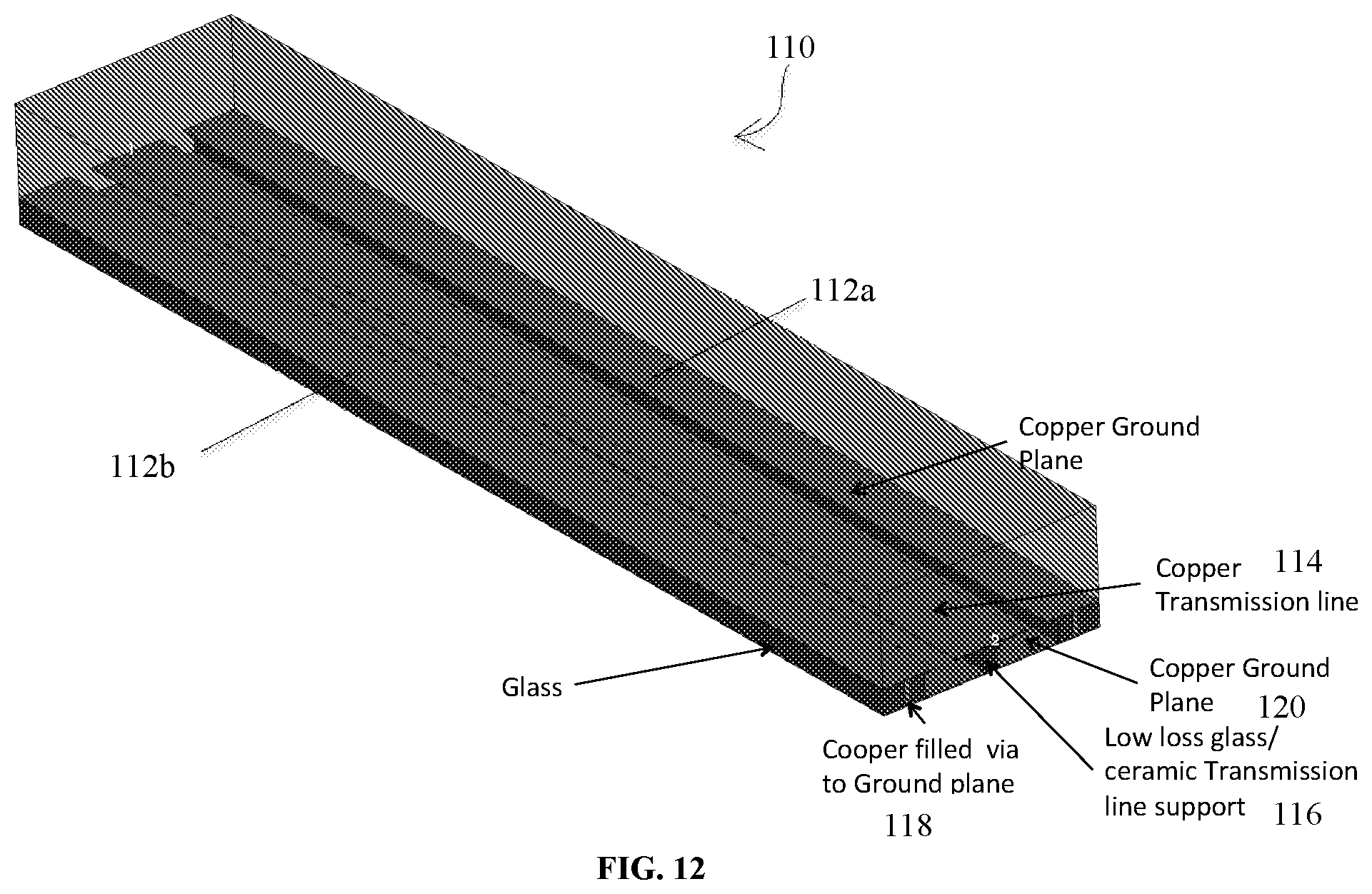
[0055] There are many RF transmission line dies on a single wafer where the specific number of die are a function of the wafer diameter. The substrate is 6'' in diameter is exposed with approximately 20 J/cm.sup.2 of 310 nm light. FIG. 12 shows a detailed, isometric schematic of a low loss transmission line 110 with a glass ceramic support. In FIG. 12, two rectangular top ground plane structures 112a, 112b ranging from 200 .mu.m to 5 .mu.m (in some cases 50 .mu.m) in width are shown, where the top ground plane structures 112a, 112b are the same length as the transmission line 114 (e.g., a copper or other conductive material). The transmission line 114 can range from 1,000 .mu.m to 5 .mu.m in width (in some cases 200 .mu.m in width) and can range from 50 .mu.m to 1 .mu.m in thick (in some cases 10 .mu.m thick). The transmission line 114 is supported by a glass ceramic pedestal 116. The interior of the pedestal 116 is of the ceramic phase of the photodefinable glass. The pedestal can range from 200 .mu.m to 5 .mu.m in thickness and (in some cases 100 .mu.m thick). The glass phase of the pedestal 116 can range from 2% to 90% of the exterior thickness of the pedestal (in some cases 20% of exterior pedestal). As an example, a 10 .mu.m glass pedestal 114 would have a ceramic phase center of 6 .mu.m to forming the glass/ceramic pedestal with 2 .mu.m of glass phase as the support pedestal of the transmission line 114. The ceramic core can have a loss tangent and dielectric constant 30% less than the glass. Glass thickness is ranges form 750 .mu.m to 50 .mu.m (in some cases 200 .mu.m). The top copper ground planes 112a, 112b, range form 200 .mu.m to 5 .mu.m (in some cases 30 .mu.m). The copper filled via 118 range from 200 .mu.m to 5 .mu.m in diameter (in some cases 50 .mu.m diameter) and connects the top ground plane structures 112a, 112b with a bottom ground plane 120 (e.g., a copper or other conductive material).
[0056] In one variant of FIG. 12, the present invention is also an antenna comprising one or more empty cavity structures over a glass or metal pedestal in an etched well and one or more grounds separated from the one or more transmission line structures to form the antenna.
[0057] In another aspect, the RF filter (RF transmission line filter (bandpass, low pass, high pass, shunt or notch)) has mechanical and thermal stabilization low loss tangent structure is under less than or equal to 100% of the contact area of the RF transmission line structure where the contact area between the support pedestal and transmission line is mostly a ceramic phase in the photodefinable glass. In another aspect, the RF transmission line has mechanical support under it, which is less than 50% of the contact area of the RF transmission line structure where the contact area of the support pedestal and transmission line is mostly a ceramic phase in the photodefinable glass. In another aspect, the RF transmission line has RF transmission line structure where the contact area of the support pedestal and transmission line is mostly a ceramic phase in the photodefinable glass. In another aspect, the RF transmission line has mechanical and thermal stabilization structure is under less than 5% of the contact area of the RF transmission line structure where the contact area of the support pedestal and transmission line is mostly a ceramic phase in the photodefinable glass. In another aspect, the RF transmission line has mechanical and thermal stabilization structure is under less than 1% of the contact area of the RF transmission line structure where the contact area of the support pedestal and transmission line is mostly a ceramic phase in the photodefinable glass. The region not in contact with the substrate is either air or a vacuum. Where the transmission line to communicate data or form a filter.
[0058] The wafer is then annealed under an inert gas (e.g., Argon) at temperature range heated between of 420.degree. C.-520.degree. C. for between 10 minutes to 2 hours, for the coalescing of silver ions into silver nanoparticles and temperature range heated between 520.degree. C.-620.degree. C. for between 10 minutes and 2 hours allowing the lithium oxide to form around the silver nanoparticles. The wafer is then coated with between 200 .ANG. and 10,000 .ANG. thick of titanium and 200 .ANG. and 10,000 .ANG. thick of copper using CVD. The wafer is then coated with photoresist and expose to the interdigitated resonate and ground plane pattern. The wafer with the interdigitated transmission line resonate pattern and ground plane (front and backside metallization connected by through glass via) and electrical contact pads are patterned in the photoresist. The wafer is then placed into a copper electroplating bath where cooper is deposited at a thickness between 0.5 .mu.m and 20 .mu.m, preferably 10 microns. The photoresist is then removed leaving the cooper coated titanium interdigitated transmission line resonate structure and ground plane and any unwanted remaining seed layer is removed using any number of well-established techniques.
[0059] The ceramic portion of the exposed/converted glass is then etched away using 10% HF solution leaving the interdigitated, ground plane and input and output structures. The wafer is then rinsed and dried using DI water and IPA.
[0060] The present inventors used a photo-definable glass ceramic (APEX.RTM.) Glass Ceramic or other photo definable glass as a novel substrate material for semiconductors, RF electronics, microwave electronics, electronic components and/or optical elements. In general, a photodefinable glass is processed using first generation semiconductor equipment in a simple three step process and the final material can be fashioned into either glass, ceramic, or contain regions of both glass and ceramic. A transmission line structures enable a wide number of filters, e.g.: Bandpass, shunt Notch, Low Pass, and High Pass used in RF circuits at frequencies from MHz to THz devices while reducing the size, cost and power consumption.
[0061] FIG. 13 shows a patch antenna structure 120 made using the present invention. An Apex glass substrate 122 includes an etched well 124, and a patch antenna 126 having a width W and a length L over the etched well 124. Often, the glass substrate 122 will have a length 2.times.L, and a width 2.times.L, or they may be varied based on the specifications of the device. The dotted lines indicate the glass mechanical support 128 under the patch antenna 126. The glass mechanical support 128 can be a pedestal or other structure that is formed by etching away the glass in the etched well 124, thus creating the glass mechanical support 128. The glass mechanical support 128 can be such that it includes the area within the dotted lines, or can also be the dotted lines itself, or combinations thereof, such that the glass mechanical support 128 supports anywhere from, e.g., 5, 10, 15, 20, 30, 45, 50, 60, 70, 75, 80, 90, or 100% of the area under the patch antenna 126. The skilled artisan, following the teachings of the present invention, can manipulate the electromagnetic features or characteristics of the patch antenna, as will be known to the skilled artisan. For example, when the patch antenna is used as an RF transmission line device, it can be designed to have a loss of less than 50, 40, 30, 25, 20, 15, or 10% of the signal input versus a signal output.
[0062] It is contemplated that any embodiment discussed in this specification can be implemented with respect to any method, kit, reagent, or composition of the invention, and vice versa. Furthermore, compositions of the invention can be used to achieve methods of the invention.
[0063] It will be understood that particular embodiments described herein are shown by way of illustration and not as limitations of the invention. The principal features of this invention can be employed in various embodiments without departing from the scope of the invention. Those skilled in the art will recognize, or be able to ascertain using no more than routine experimentation, numerous equivalents to the specific procedures described herein. Such equivalents are considered to be within the scope of this invention and are covered by the claims.
[0064] All publications and patent applications mentioned in the specification are indicative of the level of skill of those skilled in the art to which this invention pertains. All publications and patent applications are herein incorporated by reference to the same extent as if each individual publication or patent application was specifically and individually indicated to be incorporated by reference.
[0065] The use of the word "a" or "an" when used in conjunction with the term "comprising" in the claims and/or the specification may mean "one," but it is also consistent with the meaning of "one or more," "at least one," and "one or more than one." The use of the term "or" in the claims is used to mean "and/or" unless explicitly indicated to refer to alternatives only or the alternatives are mutually exclusive, although the disclosure supports a definition that refers to only alternatives and "and/or." Throughout this application, the term "about" is used to indicate that a value includes the inherent variation of error for the device, the method being employed to determine the value, or the variation that exists among the study subjects.
[0066] As used in this specification and claim(s), the words "comprising" (and any form of comprising, such as "comprise" and "comprises"), "having" (and any form of having, such as "have" and "has"), "including" (and any form of including, such as "includes" and "include") or "containing" (and any form of containing, such as "contains" and "contain") are inclusive or open-ended and do not exclude additional, unrecited elements or method steps. In embodiments of any of the compositions and methods provided herein, "comprising" may be replaced with "consisting essentially of" or "consisting of". As used herein, the phrase "consisting essentially of" requires the specified integer(s) or steps as well as those that do not materially affect the character or function of the claimed invention. As used herein, the term "consisting" is used to indicate the presence of the recited integer (e.g., a feature, an element, a characteristic, a property, a method/process step or a limitation) or group of integers (e.g., feature(s), element(s), characteristic(s), property(ies), method/process steps or limitation(s)) only.
[0067] The term "or combinations thereof" as used herein refers to all permutations and combinations of the listed items preceding the term. For example, "A, B, C, or combinations thereof" is intended to include at least one of: A, B, C, AB, AC, BC, or ABC, and if order is important in a particular context, also BA, CA, CB, CBA, BCA, ACB, BAC, or CAB. Continuing with this example, expressly included are combinations that contain repeats of one or more item or term, such as BB, AAA, AB, BBC, AAABCCCC, CBBAAA, CABABB, and so forth. The skilled artisan will understand that typically there is no limit on the number of items or terms in any combination, unless otherwise apparent from the context.
[0068] As used herein, words of approximation such as, without limitation, "about", "substantial" or "substantially" refers to a condition that when so modified is understood to not necessarily be absolute or perfect but would be considered close enough to those of ordinary skill in the art to warrant designating the condition as being present. The extent to which the description may vary will depend on how great a change can be instituted and still have one of ordinary skill in the art recognize the modified feature as still having the required characteristics and capabilities of the unmodified feature. In general, but subject to the preceding discussion, a numerical value herein that is modified by a word of approximation such as "about" may vary from the stated value by at least .+-.1, 2, 3, 4, 5, 6, 7, 10, 12 or 15%.
[0069] All of the compositions and/or methods disclosed and claimed herein can be made and executed without undue experimentation in light of the present disclosure. While the compositions and methods of this invention have been described in terms of preferred embodiments, it will be apparent to those of skill in the art that variations may be applied to the compositions and/or methods and in the steps or in the sequence of steps of the method described herein without departing from the concept, spirit and scope of the invention. All such similar substitutes and modifications apparent to those skilled in the art are deemed to be within the spirit, scope and concept of the invention as defined by the appended claims.
[0070] To aid the Patent Office, and any readers of any patent issued on this application in interpreting the claims appended hereto, applicants wish to note that they do not intend any of the appended claims to invoke paragraph 6 of 35 U.S.C. .sctn. 112, U.S.C. .sctn. 112 paragraph (f), or equivalent, as it exists on the date of filing hereof unless the words "means for" or "step for" are explicitly used in the particular claim.
[0071] For each of the claims, each dependent claim can depend both from the independent claim and from each of the prior dependent claims for each and every claim so long as the prior claim provides a proper antecedent basis for a claim term or element.
* * * * *
uspto.report is an independent third-party trademark research tool that is not affiliated, endorsed, or sponsored by the United States Patent and Trademark Office (USPTO) or any other governmental organization. The information provided by uspto.report is based on publicly available data at the time of writing and is intended for informational purposes only.
While we strive to provide accurate and up-to-date information, we do not guarantee the accuracy, completeness, reliability, or suitability of the information displayed on this site. The use of this site is at your own risk. Any reliance you place on such information is therefore strictly at your own risk.
All official trademark data, including owner information, should be verified by visiting the official USPTO website at www.uspto.gov. This site is not intended to replace professional legal advice and should not be used as a substitute for consulting with a legal professional who is knowledgeable about trademark law.