Stackable Rf Filter For A Receiver Or Transmitter
Brunette; Gilbert ; et al.
U.S. patent application number 16/676279 was filed with the patent office on 2020-05-28 for stackable rf filter for a receiver or transmitter. The applicant listed for this patent is ThinkRF Corporation. Invention is credited to Gilbert Brunette, Jeffrey Michael Hill, Jasvinder Singh Obhi, Theodore Pantazopoulos.
| Application Number | 20200168970 16/676279 |
| Document ID | / |
| Family ID | 70770004 |
| Filed Date | 2020-05-28 |


View All Diagrams
| United States Patent Application | 20200168970 |
| Kind Code | A1 |
| Brunette; Gilbert ; et al. | May 28, 2020 |
STACKABLE RF FILTER FOR A RECEIVER OR TRANSMITTER
Abstract
A receiver or transmitter designed for a broad range of frequencies requires a pre-select filter for incoming signals or a post-select filter for outgoing signals to minimize spurious signal responses. In conventional receivers, several discrete RF filters are used and a switched filter bank is created utilizing a large amount of space. A filter bank comprising a plurality of stacked shielded filters would enable different filter technologies and topologies to be used together, as other passive and active circuits may be combined into the one surface mountable component in order to save on PCB space.
| Inventors: | Brunette; Gilbert; (Ottawa, CA) ; Hill; Jeffrey Michael; (Ottawa, CA) ; Pantazopoulos; Theodore; (Ottawa, CA) ; Obhi; Jasvinder Singh; (Ottawa, CA) | ||||||||||
| Applicant: |
|
||||||||||
|---|---|---|---|---|---|---|---|---|---|---|---|
| Family ID: | 70770004 | ||||||||||
| Appl. No.: | 16/676279 | ||||||||||
| Filed: | November 6, 2019 |
Related U.S. Patent Documents
| Application Number | Filing Date | Patent Number | ||
|---|---|---|---|---|
| 62771217 | Nov 26, 2018 | |||
| Current U.S. Class: | 1/1 |
| Current CPC Class: | H05K 7/023 20130101; H05K 1/144 20130101; H01P 3/08 20130101; H01P 1/127 20130101; H05K 9/0039 20130101; H04B 1/16 20130101; H01P 1/203 20130101; H05K 2201/10053 20130101; H04B 1/006 20130101 |
| International Class: | H01P 1/203 20060101 H01P001/203; H04B 1/16 20060101 H04B001/16; H04B 1/00 20060101 H04B001/00; H01P 3/08 20060101 H01P003/08; H05K 9/00 20060101 H05K009/00; H05K 7/02 20060101 H05K007/02 |
Claims
1. An RF filter device for mounting on a PCB comprising: an input switch including an input for inputting an input signal, and a plurality of outputs; a filter stack including a plurality of filters, each filter connected to one of the plurality of outputs from the input switch and capable of filtering a selected frequency range; an output switch including a plurality of input ports, and an output port for outputting a filtered signal, each input port connected to one of the plurality of filters; wherein the filter stack comprises a plurality of superposed filters, each filter comprising: a filter layer; a dielectric layer on each side of the filter layer; and metal insulation layers above and below the dielectric layers for insulating each filter from other filters there above and/or there below.
2. The device according to claim 1, further comprising input conductive vias and output conductive vias extending between each filter layer and the PCB through intermediate filter layers, intermediate dielectric layers, and intermediate metal insulation layers.
3. The device according to claim 1, wherein the input switch and the output switch are mounted in or on the filter stack.
4. The device according to claim 3, further comprising: input conductive vias extending between the input switch at one of a top or a bottom of the filter stack and each filter layer, and output conductive vias extending between each filter layer and the output switch at the other of the top or the bottom of the filter stack.
5. The device according to claim 3, wherein the input switch and the output switch are integrated into sides of the filter stack.
6. The device according to claim 5, wherein the input switch comprises: an input via for receiving the input signal; a plurality of filter vias, a respective filter via extending to each filter layer; and a controller capable of selecting which of the plurality of filter vias the input via is connected.
7. The device according to claim 1, further comprising insulating conductive ground vias extending through the filter stack around a periphery thereof, insulated from each of the filter layers and connected to the metal insulating layers.
8. The device according to claim 1, wherein one of the metal insulation layers of one filter also comprises one of the metal insulation layers of one of the filters there above or there below.
9. The device according to claim 1, wherein each filter layer and each metal insulation layer includes castellations at outer edges thereof.
10. The device according to claim 1, wherein at least one filter comprises a first filter layer and a second filter layer on opposite sides of a first dielectric layer; wherein the first filter layer and the second filter layer are configured for broadside communication.
11. The device according to claim 1, wherein a first plurality of the filters extend parallel to an upper surface of the PCB; and wherein at least one of the filters extends perpendicular to the upper surface of the PCB and the first plurality of filters.
12. An RF filter stack for mounting on a PCB and including a plurality of filters, each filter configured for filtering a selected frequency range from an input signal, and configured for connecting to one of a plurality of outputs from an input switch receiving the input signal, and to one of a plurality of inputs from an output switch for outputting a filtered output signal; wherein the plurality of filters are superposed one top of another, each filter comprising: a filter layer; a dielectric layer on each side of the filter layer; and metal insulation layers above and below the dielectric layers for insulating each filter from other filters above and/or below.
13. The RF filter stack according to claim 12, further comprising input an conductive via and an output conductive via extending between each filter layer and the PCB through intermediate filter layers, intermediate dielectric layers, and intermediate metal insulation layers.
14. The RF filter stack according to claim 12, further comprising insulating conductive ground vias extending through the filter stack around a periphery thereof, insulated from the filter layers and connected to the metal insulating layers.
15. The RF filter stack according to claim 12, wherein the metal insulation layer of one filter also comprises the metal insulation layer of the filter there above or there below.
16. The RF filter stack according to claim 12, wherein at least one filter layer and at least one metal insulation layer includes castellations at outer edges thereof.
17. The RF filter stack according to claim 12, wherein at least one filter comprises a first filter layer and a second filter layer on opposite sides of a first dielectric layer; wherein the first filter layer and the second filter layer are configured for broadside communication.
18. The RF filter stack according to claim 12, wherein a first plurality of the filters extend parallel to an upper surface of the PCB; and wherein at least one of the filters extends perpendicular to the upper surface of the PCB and the first plurality of filters.
19. The RF filter stack according to claim 12, wherein each filter includes an electrical connector for mating with a corresponding electrical connector of the input switch.
20. An RF filter device for mounting on a PCB comprising: an electrical to optical transducer for converting an electrical input signal to an optical input signal; an input optical switch including at least one input for inputting the input optical signal and a plurality of outputs; an optical filter stack including a plurality of optical filters, each optical filter connected to one of the plurality of outputs from the input switch and capable of filtering a selected frequency range; an output optical switch including a plurality of inputs, and at least one output for outputting a filtered optical signal, each input connected to one of the plurality of optical filters; an optical to electrical transducer for converting the filter optical signal to a filtered electrical signal; wherein the filter stack comprises a plurality of superposed filters, each optical filter comprising: an optical filter layer; and a dielectric layer on each side of the optical filter layer.
Description
CROSS-REFERENCE TO RELATED APPLICATIONS
[0001] This application claims priority from U.S. patent application Ser. No. 62/771,217, filed Nov. 26, 2018, which is incorporated herein by reference.
TECHNICAL FIELD
[0002] The present invention relates to an RF filter, and in particular to a stacked RF filter for mounting on a printed circuit board.
BACKGROUND
[0003] When a receiver or transmitter is designed for a very broad range of frequencies, there is a need to pre-filter incoming signals or post-filter outgoing signals to minimize spurious signal responses. Typically, several discrete RF filters are used and a switched filter bank is created. The filter bank comprises a 1.times.N switch on either end interconnected by N PCB tracks, each track including a RF frequency filter, which can be selected by connecting both of the switches to the desired PCB track. Unfortunately, several issues arise from a classical filter bank design:
[0004] 1. The filter bank incurs signal loss along the PCB tracks from the switches leading to the filters. The PCB tracks can be electrically long at the given frequencies used and hence very lossy; 2. The filter bank consumes a lot of PCB floorspace; 3. Mechanical shielding between filters is usually required to enhance and maintain performance of the filters such that they dominate the expected filtering performance of the signals passing through them; and 4. Often, the filters at very high frequencies are part of the PCB design itself in order to save on component costs, but at the expense of dedicating the PCB to their performance. If the filters don't work well due to poor material properties selection, material properties control or filter design, the entire board is subject to scrapping due to poor filter performance.
[0005] Testing of conventional filters printed on the PCB itself can be difficult if not impossible depending on the frequency range or other mechanical limitations of getting test signals into and out of the filters. In particular, at very high frequencies, launching signals into and out of components with good fidelity or accuracy without making special provisions for connectors that take up board space, is very difficult. Higher frequency filters are often printed on the PCB and as such, become an integral part thereof. However, if the filter does not meet spec for some reason, e.g. etching accuracy being off, the whole board may have to be scrapped.
[0006] An object of the present invention is to overcome the shortcomings of the prior art by providing a filter bank comprising a plurality of stacked shielded filters. Additionally, mixed substrate materials may be used so that different filter technologies and topologies, as well as other passive and active circuits, may be combined into one surface mountable component. The filter stack also addresses the need for a filter bank in other circuits, such as broadband PLLs in receivers, transmitters or even signal generators, etc.
SUMMARY OF THE INVENTION
[0007] Accordingly, the present invention relates to an RF filter device for mounting on a PCB comprising:
[0008] an input switch including at least one input for inputting an input signal and a plurality of outputs;
[0009] a filter stack including a plurality of filters, each filter connected to one of the plurality of outputs from the input switch and capable of filtering a selected frequency range;
[0010] an output switch including a plurality of inputs, and at least one output for outputting a filtered signal, each input connected to one of the plurality of filters;
[0011] wherein the filter stack comprises a plurality of superposed filters, each filter comprising: a filter layer; a dielectric layer on each side of the filter; and metal insulation layers above and below the dielectric layers for insulating each filter from other filters above and/or below.
[0012] Another aspect of the present invention relates to an RF filter stack for mounting on a PCB and including a plurality of filters, each filter capable of filtering a selected frequency range from an input signal, and capable of connecting to one of a plurality of outputs from an input switch receiving the input signal, and to one of a plurality of inputs from an output switch for outputting a filtered output signal;
[0013] wherein the filter stack comprises a plurality of superposed filters, each filter comprising: a filter layer; a dielectric layer on each side of the filter; and metal insulation layers above and below the dielectric layers for insulating each filter from other filters above and/or below.
BRIEF DESCRIPTION OF THE DRAWINGS
[0014] The invention will be described in greater detail with reference to the accompanying drawings which represent preferred embodiments thereof, wherein:
[0015] FIG. 1 is a schematic diagram of a RF filter device in accordance with an embodiment of the present invention;
[0016] FIG. 2 is a side view of a filter stack of the RF filter device of FIG. 1;
[0017] FIG. 3A is a cross-sectional view of an alternate embodiment of a filter stack of the RF filter device of FIG. 1;
[0018] FIG. 3B is a bottom view of the filter stack of FIG. 3A;
[0019] FIG. 4 is a cross-sectional view of an alternate embodiment of a filter stack of the RF filter device of FIG. 1;
[0020] FIG. 5 is a cross-sectional view of an alternate embodiment of an RF filter device;
[0021] FIG. 6A is a cross-section view of an alternative embodiment of an RF filter device;
[0022] FIG. 6B is a top view of the RF filter device of FIG. 6A;
[0023] FIG. 6C is a top view of an alternative embodiment of the RF filter device of FIG. 6A;
[0024] FIG. 7 is a top view of an alternative embodiment of an RF filter device;
[0025] FIG. 8 is a top view of an alternative embodiment of an RF filter device;
[0026] FIG. 9 is a cross-sectional view of an alternative embodiment of the RF filter stack of FIG. 1;
[0027] FIG. 10A is a top view of an alternative embodiment of an RF filter device;
[0028] FIG. 10B is a cross-section view of the embodiment of FIG. 10A.
DETAILED DESCRIPTION
[0029] While the present teachings are described in conjunction with various embodiments and examples, it is not intended that the present teachings be limited to such embodiments. On the contrary, the present teachings encompass various alternatives and equivalents, as will be appreciated by those of skill in the art.
[0030] An RF filter device 1 of the present invention may comprises an input switch 2, an RF filter stack 3 comprised of a plurality of superposed filters 20.sub.i to 20.sub.n, and an output switch 4. The input switch 2 includes at least one input or input port 11, and a plurality of outputs or output ports 12, but a plurality of inputs or input ports 11 is also possible. Similarly, the output switch 4 includes a plurality of inputs 13 and at least one output 14, but a plurality of outputs 14 is also possible. Each output 12 of the input switch 2 is connected to one of the inputs 13 of the output switch 4 via a filter in the filter stack 3. The RF filter device 1 may be mounted on a printed circuit board (PCB) 10 utilizing conventional multi-pin or ball-grid array; however, an arrangement using connectors is also possible, as hereinafter described. The filter stack 3 also enables the filters 20 to be tested individually to ensure their performance is met before being mounted on the PCB 10.
[0031] Each filter 20.sub.i-20.sub.n may include an RF bandpass filter providing a very wide range of filtering for an RF spectrum analyzer, e.g. from 0.10 MHz to 40 GHz. For example: the frequency ranges for each filter 20.sub.i-20.sub.n may include any combination of a plurality of RF ranges, e.g. five, including Very High RF (8.0-40.0 GHz), High RF (3.0-8.0 GHz), Mid RF (400 MHz-4.4 GHz), Low RF (40-1000 MHz) and Very low RF (0.1-50 MHz).
[0032] With reference to FIGS. 2 and 3A, each filter 20.sub.i-20.sub.n of the filter stack 3 may include input connectors 21 on one or more sides and output connectors 22 on the other free sides, or a combination of input connectors 21, output connectors 22 and ball grid array (BGA) contacts 51, as hereinafter described. The input connectors 21 mounted on a side of each filter 20.sub.i-20n may correspond to a mating connector 23 on a suitable multi-connector device 25, mounted on a side of the RF filter stack 3. Similarly, the output connectors 22 mounted on the same side or a different side, e.g. opposite side, of each filter 20.sub.i to 20n may correspond to a mating connector 24 on a suitable multi-connector device 26, mounted on a side, e.g. opposite the multi-connector device 25, of the RF filter stack 3. The connectors 21-24 may comprise any suitable miniature connectors, such as AMMC (Amphenol Micro-Miniature Coaxial) connectors. The multi-connector devices 25 and 26 may be electrically connected to traces on the PCB 10 or to an external wiring, e.g. ribbon, array. Only four filters 20.sub.i to 20n are illustrated in FIG. 2, and only three filters 20.sub.i-20.sub.iii are illustrated in FIG. 3A; however, more or less filters may be included. Each filter 20.sub.i to 20n may include a plurality of layers in the filter stack 3. For example, a simple strip-line filter, illustrated in FIG. 2, may include a first ground layer 34, a signal filter layer 31, plus a second ground layer 34. The ground layers 34 may be re-used for the next stacked strip-line filter 20.sub.i-20n so the total number of layers may not match or even be a multiple of the number of filters n.
[0033] With reference to FIG. 3A, each of the filters 20.sub.i-20.sub.n may comprise a planar metallization filter layer 31i-31n (only three layers 31ii-31ii are illustrated for simplicity) on a dielectric substrate 32i-32n. There may be another upper dielectric layer 33i-33n above the filter layer 31i-31n, whereby each filter layer 31i-31n may be sandwiched between two dielectric layers, i.e. the dielectric substrate 32i-32n and the upper dielectric layer 33i-33n, respectively. The dielectric layers, i.e. the dielectric substrate 32i-32n and the upper dielectric layer 33i-33n, may have metallization or ground layers 34 applied to them at their outer parallel planar surfaces. The metallization or ground layers 34 may provide the isolation boundaries between adjacent filters 20.sub.i-20.sub.n including the filter layer 31i-31n sandwiched between dielectric layers, i.e. the dielectric substrate 32i-32n and the upper dielectric layer 33i-33n.
[0034] The dielectric substrates 32i-32n, may be electrically insulative, e.g. fiberglass, ceramic or glass, although semiconductor material might also be used, which would allow for one or more of the filters 20.sub.i-20.sub.n to be used for optical instead of electrical purposes. For example LiNbO.sub.3 or other transparent or semi-transparent material, would also allow for opto-electrical components designs, such as a Mach-Zehnder modulators acting as filters etc, as herein after discussed.
[0035] The ground layers 34 above and below each filter 20.sub.i-20.sub.n may also provide a means to insulate each filter 20.sub.i-20.sub.n from the other filters 20.sub.i-20.sub.n by forming a shielded layer. In particular, when castellations 42 (FIG. 3B) are provided around the perimeter of some or all of the layers of the RF filter stack 3 and/or interconnecting stack ground vias 41 are provided that electrically connect all the ground layers 34, multiple Faraday cages may be formed around each filter 20.sub.i-20.sub.n, thereby providing the insulated/isolating function. The stack ground vias 41 may be provided in a single or double row of ground vias 41 extending through the RF filter stack 3 around the periphery thereof in contact with each ground layer 34, but insulated from each filter layer 31i to 31n; however, any suitable arrangement, is possible. Individual signal ground vias 52i to 52n may also be provided for isolating individual signals from each filter layer 31i-31n from other filter layers 31i-31n. The signal ground vias 52i to 52n extend from the corresponding filter layer 31i-31n, respectively, and through, i.e. insulated from, lower filter layers 31ii to 31n. The signal ground vias 52i to 52n may surround or at least partially surround a central signal conductive via 55.
[0036] The sequence of the filters 20.sub.i to 20n may be in any order in the RF filter stack 3, and may be set up to minimize coupling between adjacent frequency filters 20.sub.i-20.sub.n or to accommodate other criteria, such as path loss, etc. In the case of path loss optimization for example, the highest frequency filter 20.sub.i may be placed at the bottom of the RF filter stack 3 to minimize via signal path length and loss by maximizing the number of stack ground vias 41 and signal ground vias 52i to 52n surrounding the filter layer 31i to 31n.
[0037] Passive and active components 45 may be incorporated onto each RF filter stack 3 or into each filter layer 31i-31n for loss equalization. For example, passive low pass and/or high pass filter components, e.g. attenuators, capacitors and resistors, may be incorporated into each filter layer 31i-31n to enhance the filtering of each bandpass filter 20.sub.i-20.sub.n. The active components 45 may be powered and controlled through interconnections from the bottom of the filter stack 3. Similarly, their information signals would use connections similar to the ones interconnecting the filters 20.sub.i-20.sub.n to the PCB 10 upon which the component is mounted.
[0038] With reference to FIGS. 3A and 3B, when not using input and output connectors 21 and 22, the RF filter stack 3 may make use of a ground-signal-ground pattern of metalized contacts 51 with different sets of signal ground vias 52i-52n extending through intermediate layers via insulated openings to each corresponding filter layer 31i to 31n, e.g. vias 52ii extending to filter layer 31ii, such that the signal conductive via 55ii would be locally shielded by the nearby signal ground vias 52ii. The edges of the RF filter stack 3 may be shielded with a continuous or contiguous conducting arrangement, e.g. by including multiple rows of staggered stack ground vias 41 disposed around the outer edge of the filter stack 3, thereby surrounding the signal ground vias 52i-52n. Alternatively or in addition, the edges of each filter 20.sub.i-20.sub.n may include the castellations 42. Metal deposition may also be provided around the edges of and/or between the filters 20.sub.i-20n. Each filter 20.sub.i-20.sub.n may include a different combination of insulative protection, e.g. ground vias, castellations and metallization than other filters 20.sub.i-20.sub.n in the same RF filter stack 3.
[0039] With reference to FIG. 4, an alternative embodiment of the RF filter stack 3' is configured for broadside coupling where vertical coupling is provided between adjacent metallized filter layers, e.g. 131i with 131ii, and 131iii with 131iv Each of the filters 20.sub.i and 20ii may comprise first and second planar metallization filter layer 131i/131ii and 131iii/131iv (only two filter layers 131i-131iii and two filters 20.sub.i and 20.sub.n are illustrated for simplicity) on opposite sides of a dielectric substrate 132i and 132ii. There may be a lower dielectric layer 133i (133iii) below the first filter layer 131i (131iii), and an upper dielectric layer 133ii (133iv) above the second filter layer 131ii (131iv), whereby the filter layers 131i and 131ii (131iii and 131iv) may be sandwiched between two dielectric layers, i.e. the lower and upper dielectric layers 133i and 133ii (133iiiand 133iv), but without a grounded metallization layer or shielding of any kind therebetween, enabling broadside communication between adjacent unprotected filter layers 131i and 131ii or 131iii and 131iv. However, part of a filter design may include grounded metallization, but not such that it would be meant to be shielding in nature e.g. only as a stub of a filter 131i to 131iv that happens to be grounded. The two outside (lower and upper) dielectric layers 133i/133ii and 133iii-133iv may then have metallization or ground layers 134 applied to them at their outer parallel planar surfaces. The metallization or ground layers 134 may provide the isolation boundaries between adjacent filters 20.sub.i and 20.sub.ii. The filter layers, e.g. 131i and 131ii may also be formed on upper surfaces of superposed dielectric substrates, e.g. 133i and 132i (133iii and 132ii), or on separate opposed dielectric substrates, e.g. 133i and 133ii (133iii and 133iv), with an intermediate dielectric layer, e.g. 132i (132ii), therebetween. Accordingly, every two filter layers, e.g. 131i/131ii and 131iii/131iv may only be separated from each other by one dielectric layer, e.g. dielectric substrate 132i or 132ii, but separated from other pairs of filter layers, e.g. filter layers 131iii and 131iv, by two dielectric layer, e.g. upper dielectric layer 133ii and lower dielectric layer 133iii and a metallization or ground layer 134.
[0040] The dielectric substrates, e.g. 132i-132ii and 133i-133iv, may be electrically insulative, e.g. fiberglass, ceramic or glass, although semiconductor material might also be used, which would allow for one or more of the filters 20.sub.i-20.sub.n to be optical instead of electrical. For example, LiNbO.sub.3 or other transparent or semi-transparent material could be used which would allow for opto-electrical component designs, such as a Mach-Zehnder modulator.
[0041] As described above, the ground layers 134 also provide a means to insulate each filter 20.sub.i-20.sub.n from the other filters 20.sub.i-20.sub.n by forming a shielded layer. In particular, when combined with castellations 42 around the perimeter of the stack 3, and interconnecting stack ground vias 41 and signal ground vias 52i to 52iii that electrically connect all the ground layers 134 forming multiple Faraday cages around each the filters 20.sub.i-20.sub.n, thereby providing the insulated/isolating function.
[0042] As above, when not using input and output connectors 21 and 22, the filter stack 3' may make use of a ground-signal-ground pattern of metalized contacts 51 with different sets of signal ground vias 52i-52n and signal conductive vias 55i to 55n extending through intermediate layers via insulated openings to each corresponding filter layer 31i to 31n, e.g. signal ground vias 52ii and signal conductive vias 55ii extending to filter layer 31ii, such that the signal conductive vias 55i to 55iv may be locally shielded by the nearby signal ground vias 52ii. The edges of the filter stack 3' may be shielded with a continuous or contiguous conducting arrangement, e.g. by including multiple rows of staggered stack ground vias 41 disposed around the outer edge of the filter stack 3' surrounding the signal conductive vias 55i-55n. Alternatively or in addition, the edges of each filter 20i-20n may include castellations 42. Metal deposition may also be provided around the edges of and/or between filters 20.sub.i-20.sub.n.
[0043] With the exception of vertical coupling, the filters 20.sub.i-20.sub.n may be individually shielded with interstitial ground layers 134 where the filters 20.sub.i-20.sub.n would be stacked above the first filter 20 at the bottom of the stack 3'. The ground layers 134 may be all interconnected to form one complete ground path.
[0044] In alternative embodiment illustrated in FIGS. 5, the input and output switches 2 and 4 may interface into and out of a filter stack 103, which may have a filter layer, dielectric layer and ground layer structure similar to filter stack 3, 3' or 3'', such that the switching is done inside or on the filter stack 103. According to the illustrated embodiment, the input and output switches 2 and 4 may be disposed within the filter stack 103, e.g. on top, within or beneath for inputting and outputting signals, respectively, from the filter stack 103. Ideally, the input switch 2 is located, e.g. on the bottom, at an opposite end of the filter stack 103 than the output switch 4, e.g. on the top, but any suitable arrangement is possible. Instead of all of the ground signal vias 52i-52n and signal conductive vias 55i to 55n extending down to the PCB 10, input vias 52i-52n and 55i-55n may extend from the input switch 2 to the corresponding filter layer 31i-31n, and output vias 62i-62n and 65i-65n would extend from the corresponding filter layer 31i-31n to the output switch 4. Accordingly, only one input 11 and one output 14, along with main output via 63 extending from the output switch 4 down through the filter stack 103 to the main output 14 is needed for the signal path, with additional control vias 66 and 67 extending from the input switch 2 to the output switch 4 being used for control and power from the PCB 10 and external control and power sources.
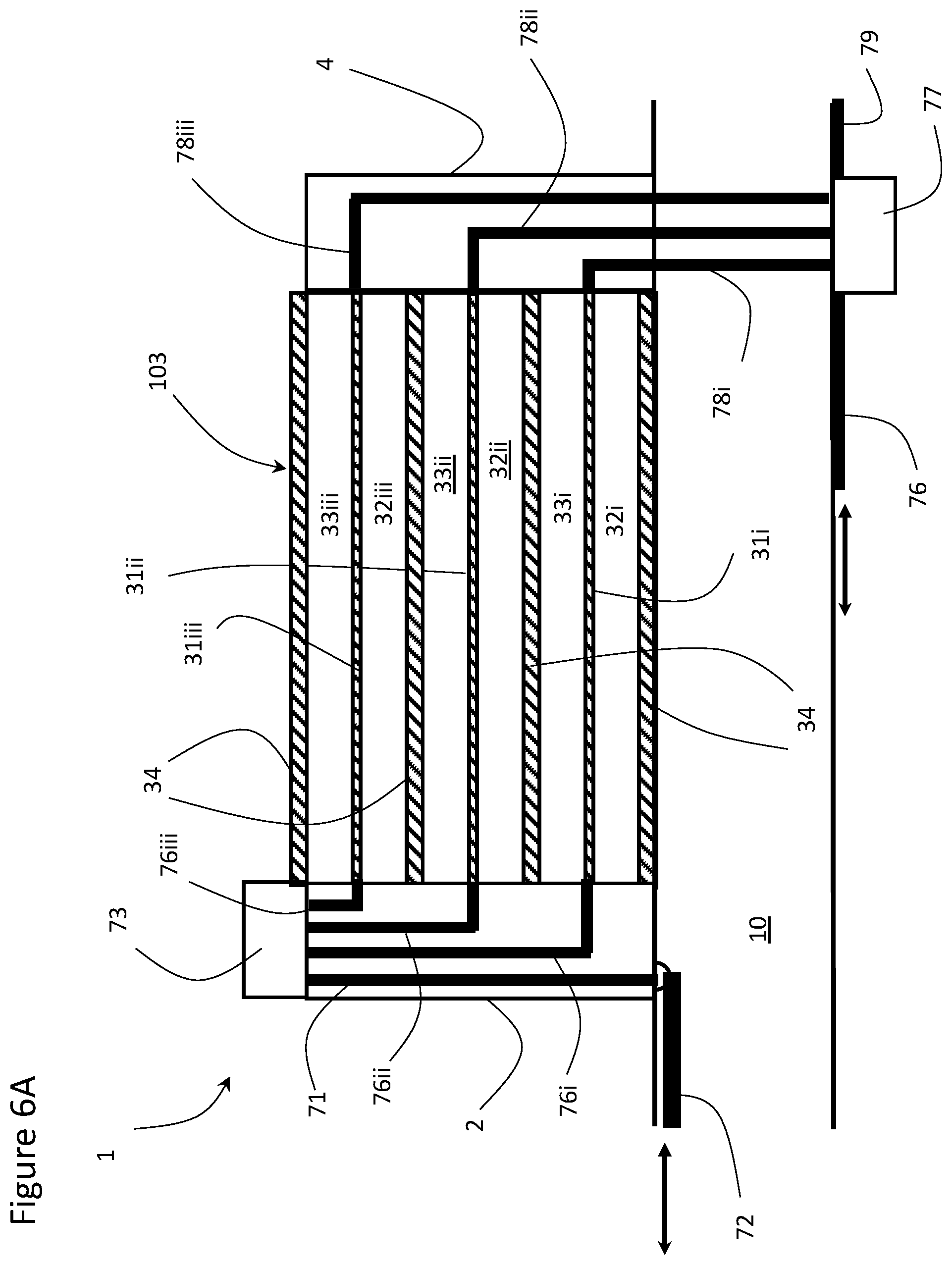
[0045] Alternatively, as illustrated in FIGS. 6A-6C, the input and output switches 2 and 4 may be electrically connected indirectly or directly at the opposite sides of the filter stack 103 (FIG. 6B), e.g. as separate integrated circuits, or integrated into or onto the side of the stack 3 (FIGS. 6A and 6C) and extending vertically up the height of the stack 103, which may have a filter layer, dielectric layer and ground layer structure similar to filter stack 3, 3' or 3''. Alternatively, each of the switches 2 and 4 may be a separate chip mounted on the PCB 10 with electrical connections extending to and from the filter stack 103. In the illustrated embodiment, for the input switch 2, signal, power and control vias 71 extend from traces 72 on the PCB 10 up to a controller 73, e.g. digital, mounted on top of the input switch 2 and the stack 3. The controller 73 may then be instructed to connect the signal via 71 to whichever filter layer 31i-31iii is desired using a selected one of the filter vias 76i-76iii. The output switch 4 may have a similar construction with control and power vias 76 extending to a controller 77 on top of the stack 103, which selects which filter via 78i-78iii, i.e. which filter layer 31i-31iii, is connected to output traces 79 on the PCB 10. Alternatively, as illustrated in FIG. 6A, the controller 77 may be positioned on the backside of the PCB 10 with the filter vias 78i-78iii extending from each filter layer 31i-31iii down through the output switch 4 and the PCB 10 to the controller 77. The control and power vias 76 and the output traces 79 may also be provided on the backside of the PCB 10. The input switch 2 may also be arranged the same way as the output switch 4, with the controller 73 on the backside of the PCB 10. As illustrated in FIG. 6C, the filter stack 103 may be arranged to maximize the length of the filter layer 31i-31n by launching the input signal in a corner of the filter stack 103 and travel diagonally across the filter stack 103 to exit the opposite corner.
[0046] For RF filter devices 1 with a large number of filters 20i-20.sub.n, another embodiment, illustrated in FIG. 7, may comprise the square filter stack 103, as seen from above, in which a first portion, e.g. approximately 1/3 to 2/3, of the outputs 12.sub.1 to 12.sub.n from the input switch 2 may be on one side of the filter stack 103, with a second portion, e.g. approximately 1/3 to 2/3, of the inputs 13.sub.1 to 13.sub.n to the output switch 4 may be on the opposite side. The outputs, e.g. outputs 125 to 128, for the second portion, e.g. half, of the filters 20.sub.i-20.sub.n from the input switch 4 being on one of the other free sides, e.g. perpendicular side, of the filter stack 103 with the corresponding outputs, e.g. inputs 13.sub.5 to 13.sub.8, to the output switch 4 on an opposite side thereof, e.g. a side perpendicular to the first output side. This arrangement enables close-in compact switch routing to and from the filter stack 103. Alternatively, the filter stack 103 may be broken up into multiple stacks, such that two or more signal outputs 12 and inputs 13 may be available per side up to the input and output switches 2 and 4. The interconnections of the input and output switches 2 and 4 with the filters 20.sub.i-20.sub.n may be all done internally to the filter stack 103, as in FIG. 6C.
[0047] For RF filter devices 1 with a large number of filters 20.sub.i-20.sub.n, e.g. used for two different purposes and/or two different signals, another embodiment of the present invention, illustrated in FIG. 8, may comprise the square filter stack 103 as seen from above in which all of the outputs 12i.sub.1 to 12i.sub.n from a first input switch 2i forming a first portion, e.g. 1/3 to 2/3, of the total inputs for the filter stack 103 may be on one side of the filter stack 103 with the corresponding inputs 13i.sub.1 to 13.sub.n from a first output switch 4i on the opposite side of the filter stack 103. All of the outputs 12ii.sub.1 to 12ii.sub.n from a second input switch 2ii, which form a second portion, e.g. 1/3 to 2/3, of the total inputs of the filters 20.sub.i-20n being on one of the other free sides, e.g. perpendicular side, with the corresponding inputs 13ii.sub.1 to 13ii.sub.n and second output switch 4ii on an opposite side thereof, e.g. perpendicular to the first output side. This arrangement enables close-in compact switch routing to and from the filter stack 103. Alternatively, the filter stack 103 may be broken up into multiple stacks, such that two or more signal outputs 12 and inputs 13 may be available per side up to the two or more input and output switches 2 and 4. The interconnections of the input and output switches 2 and 4 with the filters 20.sub.i-20.sub.n may be all done internally to the filter stack 3, as in FIG. 6c.
[0048] The filters 20.sub.i-20.sub.n in the filter stack 103 may alternate vertically from one input switch 2i to the other input switch 2ii, e.g. odd numbered filters 20i, 20iii and 20v may be connected to the first input switch 2i, while even numbered filters 20ii, 20iv and 20vi may be connected to the second input switch 2ii, but any arrangement of filters 20i-20n is possible.
[0049] Another embodiment, illustrated in FIG. 9, would enable 3D operation, in which at least one of the filters, e.g. 20iv and 20v extends perpendicularly to one or more of the other filters, e.g. 20i-20iii, whereby the filtering process may be enabled to be both in the vertical and horizontal planes, not restricting the filtering to being horizontal or completely coplanar in nature. The control, power and signal traces may all be provided in the PCB 10. The vertical ground layers 34v may be interconnected with the horizontal ground layers 34h and provide additional shielding for the side of the horizontal filters, e.g. filters 20.sub.i-20.sub.iii. A plurality of the vertical filter layers, e.g. 31iv and 31v may be electrically connected by a horizontal via 75 extending through one or more of the vertical ground layers 34v and one or more of the dielectric substrates, e.g. 32iv and 33v.
[0050] Another variation would allow for a waveguide cavity filter operation where the cavity would be wide but not very high. One example of this would be using substrate integrated waveguide (SIW) or just dielectric filled rectangular waveguides. Magnetic or electric field coupling into and out of the waveguide may also be provided.
[0051] Another embodiment of the present invention, illustrated in FIGS. 10A and 10B enables optical up-conversion of the baseband (RF) signal using a suitable electrical to optical transducer 91, such that optical filters 120.sub.i-120.sub.n in a filter stack 203 may replace filter layers 20.sub.i-20.sub.n, and the filtering may be done in the optical domain before being down-converted back to baseband (RF) using a suitable optical to electrical transducer 92. Furthermore, optical switches 102 and 104 may replace input and output switches 2 and 4. This arrangement would enable the optical filters 120.sub.i-120.sub.n to be used along with electro-optical components to do the electrical-optical conversion.
[0052] In the illustrated embodiment, for the optical input switch 102, power and control vias 171 extend from traces 172 on the PCB 10 up to a controller 173, e.g. digital, mounted on top of the optical input switch 102 and the filter stack 103. An input optical waveguide 175, e.g. fiber or integrated waveguide, transmits an input optical signal from the optical transducer 91 to the controller 173. The controller 173 may then be instructed to connect the input optical waveguide 175 to whichever filter layer 231i-231iii is desired using a selected one of the filter optical waveguides 176i-176iii. The output switch 104 may have a similar construction with control and power vias 182 extending to a controller 177 on top of or adjacent the filter stack 203, which selects which output filter waveguide 178i-178iii, i.e. which filter layer 131i-131iii, is connected to output waveguide 179 on the PCB 10. Alternatively, as illustrated in FIG. 10B, the controller 177 may be positioned on the backside of the PCB 10 with the output filter waveguides 178i-178iii extending from each filter layer 131i-131iii, down through the output optical switch 104 and the PCB 10 to the controller 177. The control and power vias 182 and the output waveguides 179 may also be provided on the backside of the PCB 10. The input optical switch 102 may also be arranged the same way as the output optical switch 104, with the controller 173 on the backside of the PCB 10.
[0053] The foregoing description of one or more embodiments of the invention has been presented for the purposes of illustration and description. It is not intended to be exhaustive or to limit the invention to the precise form disclosed. Many modifications and variations are possible in light of the above teaching. It is intended that the scope of the invention be limited not by this detailed description, but rather by the claims appended hereto.
* * * * *
D00000
D00001
D00002
D00003
D00004
D00005
D00006
D00007
D00008
D00009
D00010
D00011
D00012

D00013

D00014

XML
uspto.report is an independent third-party trademark research tool that is not affiliated, endorsed, or sponsored by the United States Patent and Trademark Office (USPTO) or any other governmental organization. The information provided by uspto.report is based on publicly available data at the time of writing and is intended for informational purposes only.
While we strive to provide accurate and up-to-date information, we do not guarantee the accuracy, completeness, reliability, or suitability of the information displayed on this site. The use of this site is at your own risk. Any reliance you place on such information is therefore strictly at your own risk.
All official trademark data, including owner information, should be verified by visiting the official USPTO website at www.uspto.gov. This site is not intended to replace professional legal advice and should not be used as a substitute for consulting with a legal professional who is knowledgeable about trademark law.