Slew-limited Output Driver Circuit
HENKER; Stephan ; et al.
U.S. patent application number 16/633336 was filed with the patent office on 2020-05-21 for slew-limited output driver circuit. This patent application is currently assigned to RACYICS GMBH. The applicant listed for this patent is RACYICS GMBH. Invention is credited to Monika DIETRICH, Stephan HENKER.
| Application Number | 20200162072 16/633336 |
| Document ID | / |
| Family ID | 63108580 |
| Filed Date | 2020-05-21 |
| United States Patent Application | 20200162072 |
| Kind Code | A1 |
| HENKER; Stephan ; et al. | May 21, 2020 |
SLEW-LIMITED OUTPUT DRIVER CIRCUIT
Abstract
A slew-limited output driver circuit facilitates finding a circuitry that allows a flexible setting of the slew-rate of an integrated circuit, with only a small footprint and latency, and which allows realizing different driver modes without additional components integrated protection against ESD. A short circuit will be solved by a slew-limited output driver circuit comprising a switchable current mirror providing an output current equal to an input current, wherein the current mirror is controlled by an additional switch, which is switched in response to control signals and/or an output current level of the output driver circuit, wherein adjustable operating modes of the slew-limited output driver circuit are realized by the control signals.
| Inventors: | HENKER; Stephan; (Nossen, DE) ; DIETRICH; Monika; (Dresden, DE) | ||||||||||
| Applicant: |
|
||||||||||
|---|---|---|---|---|---|---|---|---|---|---|---|
| Assignee: | RACYICS GMBH Dresden DE |
||||||||||
| Family ID: | 63108580 | ||||||||||
| Appl. No.: | 16/633336 | ||||||||||
| Filed: | August 3, 2018 | ||||||||||
| PCT Filed: | August 3, 2018 | ||||||||||
| PCT NO: | PCT/EP2018/071117 | ||||||||||
| 371 Date: | January 23, 2020 |
| Current U.S. Class: | 1/1 |
| Current CPC Class: | H03K 19/0005 20130101; H03K 19/01721 20130101; H03K 17/166 20130101 |
| International Class: | H03K 17/16 20060101 H03K017/16; H03K 19/00 20060101 H03K019/00; H03K 19/017 20060101 H03K019/017 |
Foreign Application Data
| Date | Code | Application Number |
|---|---|---|
| Aug 4, 2017 | DE | 10 2017 117 778.7 |
Claims
1. Slew-limited output driver circuit comprising a switchable current mirror providing an output current equal to an input current, wherein the current mirror is controlled by means of an additional switch, which is switched in response to control signals and/or an output current level of the output of the output driver circuit, wherein adjustable operating modes of the slew-limited output driver are realized by the control signals.
2. The slew-limited output driver circuit according to claim 1, wherein the switchable current mirror comprises a first current mirror and a second current mirror, wherein each current mirror comprises a lead transistor and an output transistor.
3. The slew-limited output driver circuit according to claim 2, wherein when the lead transistor of the first and/or second current mirror is switched as a diode, the output functions as a current driver with high internal resistance.
4. The Slew-limited output driver circuit according to claim 1, wherein when the additional switch at the lead transistor of the first and/or second current mirror is open, the output functions as a voltage source with low internal resistance.
5. The slew-limited output driver circuit according to claim 1, wherein the control signals control a pull-up driver and a pull-down driver comprising pass transistors, and the current mirror switch.
6. The slew-limited output driver circuit according to claim 5, wherein the control signals are switched separately from each other.
7. The slew-limited output driver circuit according to claim 1, wherein when said control signals p_prectl and p_fbe are high and n_prectl and n_fbe are low the operating mode of the output driver is a voltage source mode, wherein a slew-rate of the slew-limited driver is not limited.
8. The slew-limited output driver circuit according to claim 1, wherein when said control signals p_prectl and n_fbe are low and n_prectl and p_fbe are high the operating mode of the output driver is a current source mode, wherein the slew-rate of the slew-limited driver is limited.
9. The slew-limited output driver circuit according to claim 1, wherein when said control signals p_prectl and n_prectl are in a tri-state Z, p_fbe is low and n_fbe is high the operating mode of the output driver is automatically switched into a voltage source mode or into a current source mode if a change in the output current level is performed.
10. The slew-limited output driver circuit according to claim 1, wherein when there is a short circuit at the output of the output driver circuit, the output driver circuit remains in the current source mode and provides a limited output current only.
11. The slew-limited output driver circuit according to claim 1, wherein no transistor gates of the current mirror transistors and the additional switch are directly connected to the output.
12. The slew-limited output driver circuit according to claim 1, wherein the slew-limited output driver circuit provides a switchable pre-emphasis by pre-charging/discharging the switchable current mirror.
13. The slew-limited output driver circuit according to claim 1, wherein when a lead transistor of the first and/or second current mirror is switched as a diode, the output functions as a current driver with high internal resistance.
14. The slew-limited output driver circuit according to claim 2, wherein when there is a short circuit at the output of the output driver circuit, the output driver circuit remains in the current source mode and provides a limited output current only.
15. The slew-limited output driver circuit according to claim 14, wherein no transistor gates of the current mirror transistors and the additional switch are directly connected to the output.
16. The slew-limited output driver circuit according to claim 15, wherein the slew-limited output driver circuit provides a switchable pre-emphasis by pre-charging/discharging the switchable current mirror.
17. The slew-limited output driver circuit according to claim 5, wherein when there is a short circuit at the output of the output driver circuit, the output driver circuit remains in the current source mode and provides a limited output current only.
18. The slew-limited output driver circuit according to claim 17, wherein no transistor gates of the current mirror transistors and the additional switch are directly connected to the output.
19. The slew-limited output driver circuit according to claim 18, wherein the slew-limited output driver circuit provides a switchable pre-emphasis by pre-charging/discharging the switchable current mirror.
Description
[0001] The invention discloses a slew-limited output driver circuit.
[0002] With output drivers, fast rise times can cause electromagnetic emissions and noise. Furthermore, high output currents due to electro-migration reduce the life of said circuits. It is therefore desirable that an adequate limitation of the signal rise times would eliminate the disturbing effects. The signal rise times are related to the slew-rate which is defined as the change of voltage or current, or any other signal quantity, per unit of time.
[0003] In the prior art, various possibilities for limiting the rise time are known, which can be subdivided essentially into two groups: According to U.S. Pat. No. 6,441,653, namely the limitation of the output current and according to U.S. Pat. No. 7,471,111, namely the detection and adjustment of the voltage profile at the output pad of the driver.
[0004] The limitation of the output current possesses the following disadvantages: Resistors in the output path require high layout space for the resistive components, as a high current carrying capacity and thermal stability must be ensured. Furthermore, the signal level at the resistive load will be disturbed by the resulting resistive voltage divider between the driver and the current limiting. Also a dynamic change of the resistance value is difficult to manage.
[0005] If a current source as an output driver, as in U.S. Pat. No. 7,471,111, is used no low-impedance driver will be feasible and the signal level at the resistive load will be disturbed as well.
[0006] Also the detection and adjustment of the voltage curve at the output pad of the driver according to the prior art has a few disadvantages. On the one hand, if the output driver is regulated based on the output level, for example if, like in U.S. Pat. No. 6,441,653 the output current of the preamplifier is reduced in accordance with the output voltage, whereby the driver transistor is turned on slowly, it is detrimental that the recharge current of the preamplifier is partially dissipated. Furthermore, the output voltage shows a non-linear characteristic due to the variable gate voltage of the output driver, and an ESD (electrostatic discharge) protection for the transistor gate of the feedback will be necessary. On the other hand, if a reference edge is used and its replication has to be generated at the output of the output driver a high circuitry complexity is necessary, the switching speed is limited and there is a high latency in the signal path.
[0007] It is therefore the purpose of the invention to find a circuitry that allows a flexible setting of the slew-rate of an integrated circuit, with only a small footprint and latency, and which allows realizing different driver modes without additional components integrated protection against ESD and short circuit.
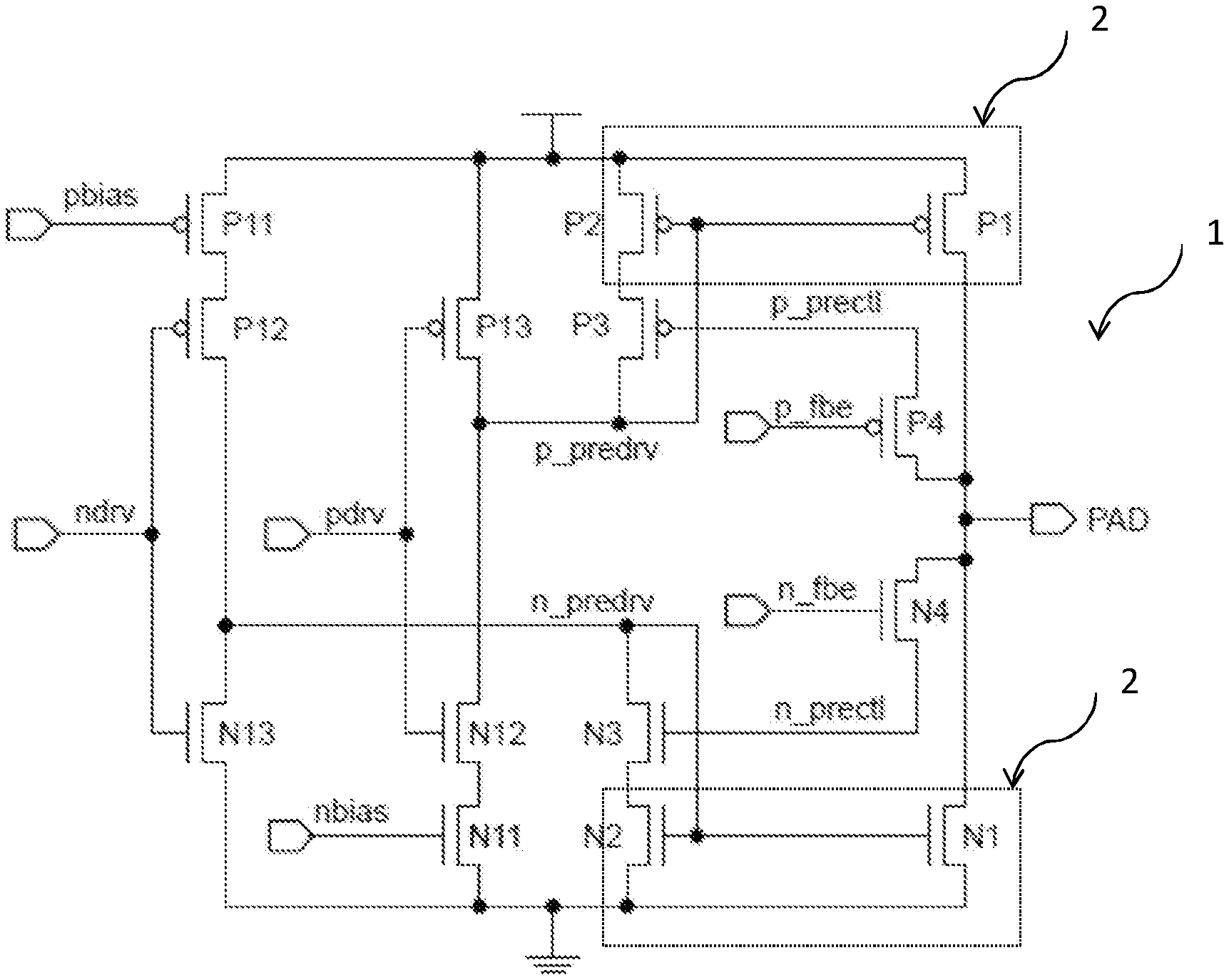
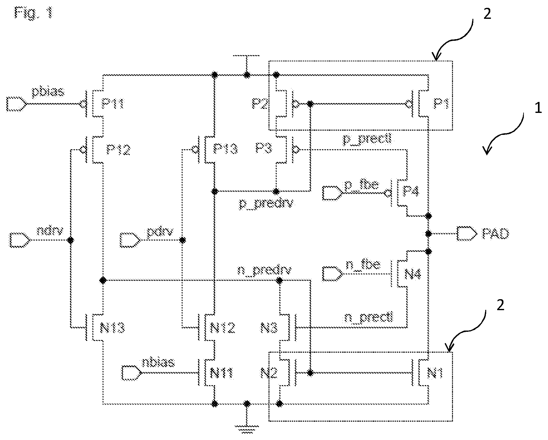
[0008] The object of the invention will be solved by a slew-limited output driver circuit comprising a switchable current mirror (P1, P2, respectively N1, N2) providing an output current equal to an input current, wherein the current mirror (P1, P2, respectively N1, N2) is controlled by means of an additional switch (P3, respectively N3), which is switched in response to control signals (prectl, fbe) and/or an output current level (PAD) of the output driver circuit, whereas adjustable operating modes of the slew-limited output driver circuit are realized by the control signals.
[0009] The core of the invention is the switchable current mirror (P1, P2 or N1, N2) which is switched by means of an additional switch (P3 or N3) in response to control signals (prectl, fbe) and/or the level at the output (PAD). The control signals prectl, fbe exist for the corresponding current mirror as p_prectl, p_fbe and n_prectl, n_fbe. The output node (PAD) provides an output current level according to the controlling and timing of the slew-limited output driver circuit.
[0010] The switchable current mirror (P1 and P2 with switch P3, N1 and N2 with switch N3 respectively) of the inventive slew-limited output driver circuit comprises a first current mirror (P1, P2) and a second current mirror (N1, N2), whereas each current mirror comprises a lead transistor (P2 or N2) and an output transistor (P1 or N1).
[0011] In a preferred embodiment of the inventive slew-limited output driver circuit, if the lead transistor (P2 or N2) of the first and/or second current mirror is switched as a diode, the output (PAD) functions as a current driver with high internal resistance. So, one or the other or both current mirrors (the first and the second current mirror) can be switched as a diode. If the lead transistor (P2 or N2) is switched as a diode, a constant gate voltage at the corresponding output transistor (P1 or N1) and thus a constant output current is generated, whereby a linear increase of the output voltage is achieved at a capacitive load. The output thus functions as a current driver with high internal resistance.
[0012] In another preferred embodiment of the inventive slew-limited output driver circuit, if the additional switch (P3 or N3) at the lead transistor (P2 or N2) of the first and/or second current mirror is open, the output (PAD) functions as a voltage source with low internal resistance. If the switch (P3 or N3) on the lead transistor (P2 or N2) is turned off, hence it is open, the gate-source voltage at the output transistor (P1 or N1) increases so that it opens completely and the output operates as a voltage source with low internal resistance.
[0013] In a further preferred embodiment of the inventive slew-limited output driver circuit, the control signals control a pull-up driver and a pull-down driver comprising pass transistors (P4, respectively N4) and the current mirror switch (P3, respectively N3). The pull-up driver is controlled by the control signals p_prectl, p_fbe and the pull-down driver is controlled by the control signals n_prectl, n_fbe.
[0014] It is preferred that the control signals are switched separately from each other. This has the effect that three different operation modes can be realized as described in the following.
[0015] In a preferred embodiment of the inventive slew-limited output driver circuit, if said control signals p_prectl and p_fbe are logic high (logic 1) and n_prectl and n_fbe are logic low (logic 0) the operating mode of the output driver is a voltage source mode, whereas a slew-rate of the slew-limited output driver circuit is not limited. Logic low or logic 0 means that the considered node is very low resistive or on ground level. Logic high or logic 1 means that the considered node is very low resistive or on supply voltage level. A tri-state means that the node is very high resistive. By adjusting the control signals in the described way above the operating mode of the slew-limited output driver circuit can be adjusted to a voltage source mode. In the voltage source mode the circuit has a low output impedance, a small rise/fall time and slew-rate is not limited.
[0016] In another preferred embodiment of the inventive slew-limited output driver circuit, if said control signals p_prectl and n_fbe are logic low (logic 0) and n_prectl and p_fbe are logic high (logic 1) the operating mode of the output driver is a current source mode, whereas the slew-rate of the slew-limited output driver is limited. In the current source mode the circuit has a high output impedance, constant output current, limited slew-rate and a linear change of output voltage on capacitive load.
[0017] In another preferred embodiment of the inventive slew-limited output driver circuit, if said control signals p_prectl and n_prectl are in a tri-state Z, p_fbe is logic low (logic 0) and n_fbe is logic high (logic 1) the operating mode of the output driver is automatically switched into a voltage source mode or into a current source mode as soon as a change in the output current level is performed. In the so-called automatic mode, the turn-off of the conducting transistor (P1 or N1) is controlled by the output voltage via a pass transistor (P4 or N4). If the output level has not yet reached the target voltage, the circuit operates as a current driver with limited output current and high internal resistance, however, if the target voltage level is reached, the circuit is automatically switched to voltage source mode with low internal resistance.
[0018] In a further preferred embodiment of the inventive slew-limited output driver circuit, if there is a short circuit at the output (PAD) of the output driver circuit, the output driver circuit remains in the current source mode and provides a limited output current only. Hence the inventive slew-limited output driver circuit provides an integrated short-circuit protection. If there is a short circuit at the output and the output level does not change, the driver remains in current source mode and provides only the limited set output current.
[0019] In a preferred embodiment of the inventive slew-limited output driver circuit, no transistor gates of the current mirror transistors and the additional switch are directly connected to the output (PAD). This has the advantage that since no transistor gates are connected directly to the output for the realization, there is no danger due to ESD events.
[0020] In a further preferred embodiment the slew-limited output driver circuit provides a switchable pre-emphasis by pre-charging/discharging the switchable current mirror. This means, that it is possible to pre-emphasize the output signal (pre-emphasis) by pre-charging or discharging the nodes p_predrv or n_predrv before the switching operation in order to improve the signal properties on lines with low-pass behavior. For this purpose, the current mirror is constructed as a high-swing cascode, which is switched at the cascode voltage. If the gate has been discharged before switching on, the output current starting from 0 will slowly increase to the set current limit (soft start); however, when the gate is charged, the output current rises rapidly to a value greater than the set current limit and then drops to the limit (this is called pre-emphasis).
[0021] The invention can be summarized by the following advantages over the prior art: Firstly, a constant output current during the switching phase of the output signal of the slew-limited output driver can be realized; secondly, the inventive circuit provides an integrated short-circuit protection; thirdly, there are different current limiting modes: a) switched off (voltage source mode), b) only active when changing level (automatic mode), c) permanently active (constant current source mode); fourthly, the inventive circuit provides a switchable pre-emphasis by pre-charging/discharging the current mirror; fifthly, only low chip area is necessary due to few additional elements; and sixthly, the feedback is inherently protected against ESD.
[0022] The invention will be explained in more detail using an exemplary embodiment.
[0023] The appended drawing shows
[0024] FIG. 1 Inventive slew-limited output driver circuit.
[0025] The FIGURE shows the inventive slew-limited output driver circuit. The inventive circuit uses in its core a current mirror (P1, P2 or N1, N2), by means of an additional switch (P3 or N3) in response to control signals (prectl, fbe) and/or the current level at the output (PAD) is switched. The control signals exist respectively for the pull-up driver (p_prectl, p_fbe) and the pull-down driver (n_prectl, n_fbe). They can be switched separately in a general embodiment.
[0026] If the lead transistor (P2 or N2) is switched as a diode, a constant gate voltage at the corresponding output transistor (P1 or N1) and thus a constant output current is generated, whereby a linear increase of the output voltage is achieved at a capacitive load. The output thus functions as a current driver with high internal resistance.
[0027] If the switch (P3 or N3) on the lead transistor (P2 or N2) is turned off, hence it is open, the gate-source voltage at the output transistor (P1 or N1) increases so that it opens completely and the output operates as a voltage source with low internal resistance.
[0028] By the control signals (prectl, fbe), the operating mode, for example the voltage source mode or the current source mode is set as shown in the following tables:
TABLE-US-00001 p_prectl p_fbe function logic 1 logic 1 voltage source mode (low resistive, (low resistive, slew-rate supply voltage) supply voltage) not limited logic 0 logic 1 current source mode (low resistive, (low resistive, slew-rate ground) supply voltage) limited Tri-state Z (high logic 0 voltage source mode, resistive) (low resistive, current source mode/ ground) slew-rate limitation will be automatically activated, if there is a level change at the output else Not allowed n_prectl n_fbe function logic 0 logic 0 voltage source mode (low resistive, (low resistive, slew-rate ground) ground) not limited logic 1 logic 0 current source mode (low resistive, (low resistive, slew-rate limited supply voltage) ground) Tri-state Z (high logic 1 voltage source mode, resistive) (low resistive, current source mode/ supply voltage) slew-rate limitation will be automatically activated, if there is a level change at the output else Not allowed
[0029] In the so-called automatic mode, the turn-off of the conducting transistor (P1 or N1) is controlled by the output voltage via a pass transistor (P4 or N4). If the output level has not yet reached the target voltage, the circuit operates as a current driver with limited output current and high internal resistance, however, if the target voltage level is reached, the circuit is automatically switched to voltage source mode with low internal resistance.
[0030] If there is a short circuit at the output and the output level does not change, the driver remains in current source mode and provides only the limited set output current.
[0031] Since no transistor gates are connected directly to the output for the realization, there is no danger due to ESD events.
[0032] In addition, it is possible to pre-emphasize the output signal (pre-emphasis) by pre-charging or discharging the nodes p_predrv or n_predrv before the switching operation in order to improve the signal properties on lines with low-pass behavior. For this purpose, the current mirror is constructed as a high-swing cascode, which is switched at the cascode voltage. If the gate has been discharged before switching on, the output current starting from 0 will slowly increase to the set current limit (soft start); however, when the gate is charged, the output current rises rapidly to a value greater than the set current limit and then drops to the limit (this is called pre-emphasis).
[0033] The essential advantage of the claimed invention is the usage of a switchable current mirror, the control of the current mirror by direct feedback of the output, and the implementation of adjustable operating modes, such as current source mode/voltage source mode/automatically switchable mode.
LIST OF REFERENCE SIGNS
[0034] 1 Slew-limited output driver circuit [0035] 2 switchable current mirror [0036] P1+P2 first current mirror [0037] N1+N2 second current mirror [0038] P1, N1 output transistor [0039] P2, N2 lead transistor [0040] P3, N3 additional switch [0041] P4 pull-up driver [0042] N4 pull-down driver [0043] x_prectl, x_fbe control signal, with x=p, n [0044] PAD output with output signal
* * * * *
D00000
D00001
XML
uspto.report is an independent third-party trademark research tool that is not affiliated, endorsed, or sponsored by the United States Patent and Trademark Office (USPTO) or any other governmental organization. The information provided by uspto.report is based on publicly available data at the time of writing and is intended for informational purposes only.
While we strive to provide accurate and up-to-date information, we do not guarantee the accuracy, completeness, reliability, or suitability of the information displayed on this site. The use of this site is at your own risk. Any reliance you place on such information is therefore strictly at your own risk.
All official trademark data, including owner information, should be verified by visiting the official USPTO website at www.uspto.gov. This site is not intended to replace professional legal advice and should not be used as a substitute for consulting with a legal professional who is knowledgeable about trademark law.