Methods And Apparatus For Nand Flash Memory
Hsu; Fu-Chang
U.S. patent application number 16/687556 was filed with the patent office on 2020-05-21 for methods and apparatus for nand flash memory. The applicant listed for this patent is NEO Semiconductor, Inc.. Invention is credited to Fu-Chang Hsu.
| Application Number | 20200160910 16/687556 |
| Document ID | / |
| Family ID | 70728103 |
| Filed Date | 2020-05-21 |

View All Diagrams
| United States Patent Application | 20200160910 |
| Kind Code | A1 |
| Hsu; Fu-Chang | May 21, 2020 |
METHODS AND APPARATUS FOR NAND FLASH MEMORY
Abstract
Methods and apparatus for NAND flash memory are disclosed. In an embodiment, a method is provided for programming a NAND flash memory includes setting programming conditions on word lines to set up programming of multiple memory cells associated with multiple bit lines, and sequentially enabling bit line select gates to load data from a page buffer to the multiple bit lines of the memory. After each bit line is loaded with selected data, an associated bit line select gate is disabled so that the selected data is maintained on the bit line using bit line capacitance. The method also includes waiting for a programming interval to complete after all the bit lines are loaded with data to program the multiple memory cells associated with the multiple bit lines. At least a portion of the multiple memory cells are programmed simultaneously.
| Inventors: | Hsu; Fu-Chang; (San Jose, CA) | ||||||||||
| Applicant: |
|
||||||||||
|---|---|---|---|---|---|---|---|---|---|---|---|
| Family ID: | 70728103 | ||||||||||
| Appl. No.: | 16/687556 | ||||||||||
| Filed: | November 18, 2019 |
Related U.S. Patent Documents
| Application Number | Filing Date | Patent Number | ||
|---|---|---|---|---|
| 62768979 | Nov 18, 2018 | |||
| 62770150 | Nov 20, 2018 | |||
| 62774128 | Nov 30, 2018 | |||
| 62783199 | Dec 20, 2018 | |||
| 62799669 | Jan 31, 2019 | |||
| Current U.S. Class: | 1/1 |
| Current CPC Class: | G11C 16/08 20130101; G11C 16/26 20130101; G11C 16/0483 20130101; G11C 11/5628 20130101; G11C 11/5642 20130101; G11C 16/32 20130101; G11C 16/3459 20130101; G11C 16/24 20130101; G11C 16/10 20130101 |
| International Class: | G11C 16/04 20060101 G11C016/04; G11C 16/10 20060101 G11C016/10; G11C 16/08 20060101 G11C016/08; G11C 16/24 20060101 G11C016/24; G11C 16/26 20060101 G11C016/26; G11C 16/32 20060101 G11C016/32; G11C 11/56 20060101 G11C011/56 |
Claims
1. A method for programming a NAND flash memory, wherein the NAND flash memory comprises a memory array having strings of memory cells that are accessed using bit lines and word lines, the method comprising: setting programming conditions on the word lines to set up programming of multiple memory cells associated with multiple bit lines; sequentially enabling bit line select gates to load data from a page buffer to the multiple bit lines of the memory, wherein after each bit line is loaded with selected data an associated bit line select gate is disabled so that the selected data is maintained in the bit line using bit line capacitance; and waiting for a programming interval to complete after all the bit lines are loaded with data to program the multiple memory cells associated with the multiple bit lines, wherein at least a portion of the multiple memory cells are programmed simultaneously.
2. The method of claim 1, wherein before the operation of setting, performing an operation of enabling bit line select gates to load a precharge voltage to multiple bit lines of the memory, and after the operation of setting, performing an operation of disabling the bit line select gates to store the precharge voltage in the multiple bit lines using a bit line capacitance associated with each bit line.
3. A method for programming a NAND flash memory, wherein the NAND flash memory comprises a memory array having strings of memory cells that are accessed using bit lines and word lines, the method comprising: sequentially enabling the bit line select gates to load data from a page buffer to multiple bit lines of the memory, wherein after each bit line is loaded with selected data an associated bit line select gate is disabled so that the selected data is maintained in the bit line using the bit line capacitance; setting programming conditions on the word lines to set up programming of multiple memory cells associated with the multiple bit lines; and waiting for a programming interval to complete after all the bit lines are loaded with data to program the selected memory cells associated with the multiple bit lines, wherein at least a portion of the bit lines are programmed simultaneously.
4. A method for reading a NAND flash memory, wherein the NAND flash memory comprises a memory array having strings of memory cells that are accessed using bit lines and word lines, the method comprising: setting reading conditions on the word lines and source lines to set up reading of multiple memory cells associated with multiple bit lines; enabling bit line select gates to load a precharge voltage to the multiple bit lines of the memory, and after the operation of enabling, disabling the bit line select gates to store the precharge voltage in the multiple bit lines using a bit line capacitance associated with each bit line, wherein the precharging voltage is different from a source line voltage; waiting for a discharging interval to complete, after all the selected memory cells are in an on-state, to discharge the associated bit lines to a predetermined voltage or current level, wherein at least a portion of the bit lines are discharged simultaneously; sequentially enabling the bit line select gates to couple the associated bit lines to a sensing circuit, that performs sensing of voltage or current level of the bit lines to determine data; latching the data into a data latch; and repeating the enabling and latching for the multiple bit lines until the data of the multiple bit lines are latched.
5. A NAND flash memory, comprising: a memory array having a plurality of bit lines and a plurality of word lines; a page buffer that stores data to be written to the memory array or data read from the memory array, wherein the page buffer includes a plurality of data lines and is configured to simultaneously program memory cells in multiple cell strings of the memory array; and bit line select gates that selectively connect each data line of the page buffer to two or more bit lines of the memory array.
6. The memory of claim 5, further comprising bit line select gate signals that selectively enable and disable the bit line select gates.
7. The memory of claim 5, wherein the page buffer comprises a sense amplifier and one or more data latches connected to each data line.
8. The memory of claim 7, wherein the page buffer is configured to perform multilevel programing, wherein the page buffer includes a latch for each bit-level to be programmed.
9. The memory of claim 7, wherein the page buffer further comprises one or more data registers connected to each data latch.
10. The memory of claim 5, wherein the memory array is divided into N sub-arrays and each sub-array is connected to through associated bit select gates to an associated page buffer having size 1/N, and wherein the total page buffer size does not change as N changes, and wherein the total size of memory cells for read operation and program operations becomes N times of a total page buffer size.
11. The memory of claim 5, wherein the page buffer is located either above or below the memory array.
12. The memory of claim 5, further comprising latch pass gates that selectively couple the data lines of the page buffer to the bit line select gates, and first pass gates that selective couple the data lines of the page buffer to bypass the bit line select gates.
13. The memory of claim 5, further comprising second pass gates the selectively couple adjacent data lines of the page buffer to each other.
14. The memory of claim 5, further comprising shielding devices coupled to the bit lines, wherein the shielding devices selectively enable a shielding voltage onto the bit lines.
15. The memory of claim 5, wherein the data lines of the page buffer are coupled to non-adjacent bit lines.
16. The memory of claim 5, wherein the memory array comprises multiple array blocks and each array block has bit lines that are coupled to associated bit line select gates, and wherein the data lines of the page buffer are global data lines that are coupled to the bit line select gates associated with all array blocks.
Description
CROSS-REFERENCE TO RELATED APPLICATIONS
[0001] This application claims the benefit under 35 U.S.C. .sctn. 119 of U.S. Provisional Patent Application No. 62/768,979, filed on Nov. 18, 2018, and entitled "NAND Flash Memory Read and Write Operations," and U.S. Provisional Patent Application No. 62/770,150, filed on Nov. 20, 2018, and entitled "NAND Flash Memory Read and Write Operations," and U.S. Provisional Patent Application No. 62/774,128, filed on Nov. 30, 2018, and entitled "NAND Flash Memory Read and Write Operations," and U.S. Provisional Patent Application No. 62/783,199, filed on Dec. 20, 2018, and entitled "NAND Flash Memory Read and Write Operations," and U.S. Provisional Patent Application No. 62/799,669, filed on Jan. 31, 2019, and entitled "NAND Flash Memory Read and Write Operations," all of which are hereby incorporated herein by reference in their entireties.
FIELD OF THE INVENTION
[0002] The exemplary embodiments of the present invention relate generally to the field of semiconductors and integrated circuits, and more specifically to the design and operation of NAND flash memory.
BACKGROUND OF THE INVENTION
[0003] Memory devices are extensively used in industrial and consumer electronics. In many cases, the limitations of the memory affect the size, performance, or cost of an industrial or consumer device, such as a mobile phone.
[0004] One type of memory that is used in many devices is called a NAND flash memory. This type of memory is organized as one or more blocks and each block includes strings of memory cells that are accessed by word lines and bit lines. Data is programmed in the memory cells or read from the memory cells using page buffers that are coupled to the bit lines. In a typical NAND flash memory, the number of the bit lines that can be program or read at one time is equal to the number of page buffers. This is referred to as `page-programming` or `page-reading`. Increasing the number of page buffers may increase the data read/write throughput, to enhance the memory performance. However, the page buffer's circuit size is quite large. It typically occupies about 20% of the memory's die size. Therefore, a typical number of page buffers is limited to a range of 16 KB to 64 KB, which limits the read/write performance of the NAND flash memory.
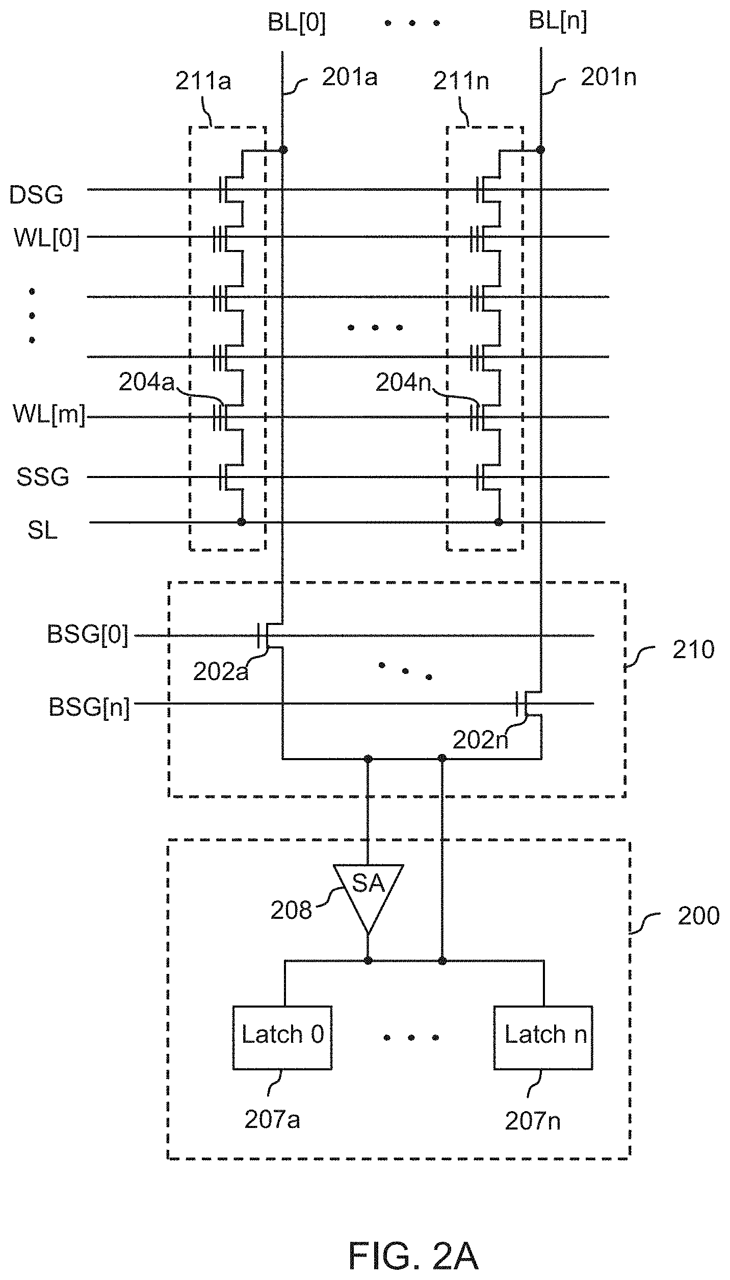
SUMMARY
[0005] In various exemplary embodiments, NAND flash memory architectures and methods are provided for use with two-dimensional (2D) or three-dimensional (3D) NAND memory arrays. Embodiments can also be applied to single-level cell (SLC), multi-level cell (MLC), triple-level cell (TLC), quad-level cell (QLC), or any number of bits per cell technology.
[0006] In an embodiment, a NAND architecture include bit line select gates that connect page buffers to a large number of bit lines to increase read/write throughput. In another embodiment, the bit line select gates couple the page buffer to non-adjacent bit lines to mitigate capacitive coupling. In other embodiments, additional pass gates and data registers are used to enhance the operation of the NAND memory. In still other embodiments, novel programming and reading operations are provided that result in increased performance.
[0007] In an embodiment, a method is provided for programming a NAND flash memory includes setting programming conditions on word lines to set up programming of multiple memory cells associated with multiple bit lines, and sequentially enabling bit line select gates to load data from a page buffer to the multiple bit lines of the memory. After each bit line is loaded with selected data, an associated bit line select gate is disabled so that the selected data is maintained on the bit line using bit line capacitance. The method also includes waiting for a programming interval to complete after all the bit lines are loaded with data to program the multiple memory cells associated with the multiple bit lines. At least a portion of the multiple memory cells are programmed simultaneously.
[0008] In an embodiment, a NAND flash memory is provided that comprises a memory array having a plurality of bit lines and a plurality of word lines, a page buffer that stores data to be written to the memory array or data read from the memory array. The page buffer includes a plurality of data lines and is configured to simultaneously program memory cells in multiple cell strings of the memory array. The memory also comprise bit line select gates that selectively connect each data line of the page buffer to two or more bit lines of the memory array.
[0009] Additional features and benefits of the present invention will become apparent from the detailed description, figures and claims set forth below.
BRIEF DESCRIPTION OF THE DRAWINGS
[0010] The exemplary embodiments of the present invention will be understood more fully from the detailed description given below and from the accompanying drawings of various embodiments of the invention, which, however, should not be taken to limit the invention to the specific embodiments, but are for explanation and understanding only.
[0011] FIG. 1A shows an exemplary block diagram of NAND flash memory architecture in accordance with embodiments of the invention.
[0012] FIG. 1B shows another embodiment of a NAND flash memory architecture constructed in accordance with embodiments of the invention.
[0013] FIG. 1C shows a detailed embodiment of a conventional 3D NAND flash memory cell array and page buffers.
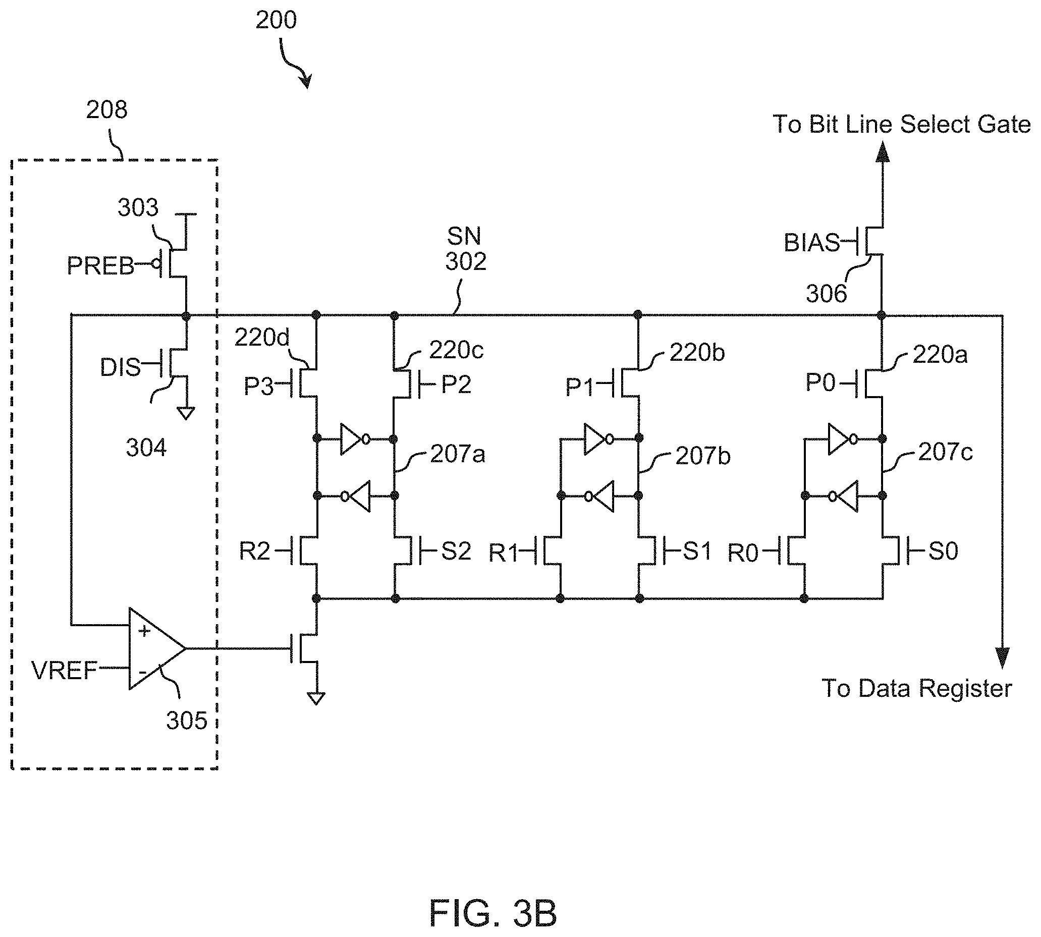
[0014] FIG. 1D shows a configuration of the conventional structure of a 3D NAND memory array.
[0015] FIG. 1E shows an embodiment of an array structure in accordance with the invention.
[0016] FIG. 1F shows an embodiment of a 3D array structure in accordance with the invention.
[0017] FIG. 2A shows an embodiment of a page buffer and bit line select gate configuration in accordance with embodiments of the invention.
[0018] FIG. 2B shows another embodiment of the page buffer configuration in accordance with embodiments of the invention.
[0019] FIGS. 2C-E show embodiments illustrating bit line select gates in accordance with the invention.
[0020] FIGS. 3A-B shows embodiments of a page buffer circuit.
[0021] FIGS. 4A-D show the operation of a page buffer and bit line select gates in accordance with the invention.
[0022] FIGS. 5A-E shows exemplary waveforms for multiple-page programming in accordance with the invention.
[0023] FIGS. 6A-C show multiple-page read operations in accordance with embodiments of the invention.
[0024] FIG. 6D shows another exemplary embodiment of a circuit in accordance with the invention.
[0025] FIGS. 7A-D show embodiments of read operation waveforms in accordance with the invention.
[0026] FIGS. 8A-C show embodiments of program and program-verify operations.
[0027] FIGS. 9A-D show NAND flash memory array architectures that are divided into sub-arrays.
[0028] FIGS. 10A-E show embodiments of 3D array architectures in accordance with the invention.
[0029] FIG. 11A shows an embodiment of a 3D array wherein the bit lines are used as temporary data storage in accordance with the invention.
[0030] FIG. 11B shows an embodiment of waveforms that illustrate how data is loaded into multiple bit lines in accordance with the invention.
[0031] FIG. 11C shows another embodiment of waveforms to load data to multiple bit lines in accordance with the invention.
[0032] FIG. 11D shows exemplary waveforms illustrating data reads from the bit line capacitors in accordance with the invention.
[0033] FIGS. 12A-B shows embodiments of a 3D array that provide SLC and TLC programming in accordance with the invention.
[0034] FIG. 13 shows an embodiment of a NAND flash memory array that illustrates bit line to bit line capacitance.
[0035] FIG. 14 shows an array having bit line shielding that is used to prevent bit line coupling.
[0036] FIGS. 15A-B show another embodiment of a circuit and corresponding waveforms for mitigating bit line-to-bit line coupling.
[0037] FIG. 16 shows an exemplary embodiment of a circuit that resolves the last bit-line coupling issue as described with reference to FIGS. 15A-B.
[0038] FIG. 17A shows an embodiment of a circuit that comprises even and odd page buffers as illustrated in FIG. 16.
[0039] FIGS. 17B-C show embodiments of 2D and 3D versions of an array (or sub-array) for use in the circuit of FIG. 17A.
[0040] FIGS. 18A-B show circuits having a divided bit line structure.
[0041] FIGS. 19A-B show another embodiment of a bit line select gate circuit and its corresponding operating waveforms in accordance with the invention.
[0042] FIGS. 20A-B show an embodiment of a circuit and associated read waveforms that address bit line coupling without sacrificing read data throughput.
[0043] FIGS. 21A-B show embodiments of a sensing circuit and associated operating waveforms in accordance with the invention.
[0044] FIGS. 22A-B show exemplary embodiments of a sensing circuit and associated waveforms in accordance with the invention.
[0045] FIGS. 23A-B show exemplary embodiments of a sensing circuit and associated waveforms in accordance with the invention.
[0046] FIGS. 24A-B show exemplary embodiments of a sensing circuit and associated waveforms in accordance with the invention.
[0047] FIGS. 25A-C show exemplary embodiments of a page buffer and bit line decoder circuit according to the invention.
DETAILED DESCRIPTION
[0048] In various exemplary embodiment, methods and apparatus for the design and operation of NAND flash memory architectures are provided that can be used with two-dimensional (2D) or three-dimensional (3D) NAND arrays. Embodiments can also be applied to single-level cell (SLC), multi-level cell (MLC), triple-level cell (TLC), quad-level cell (QLC), or any number of bits per cell technology.
[0049] Those of ordinary skilled in the art will realize that the following detailed description is illustrative only and is not intended to be in any way limiting. Other embodiments of the present invention will readily suggest themselves to such skilled persons having the benefit of this disclosure. Reference will now be made in detail to implementations of the exemplary embodiments of the present invention as illustrated in the accompanying drawings. The same reference indicators (or numbers) will be used throughout the drawings and the following detailed description to refer to the same or like parts.
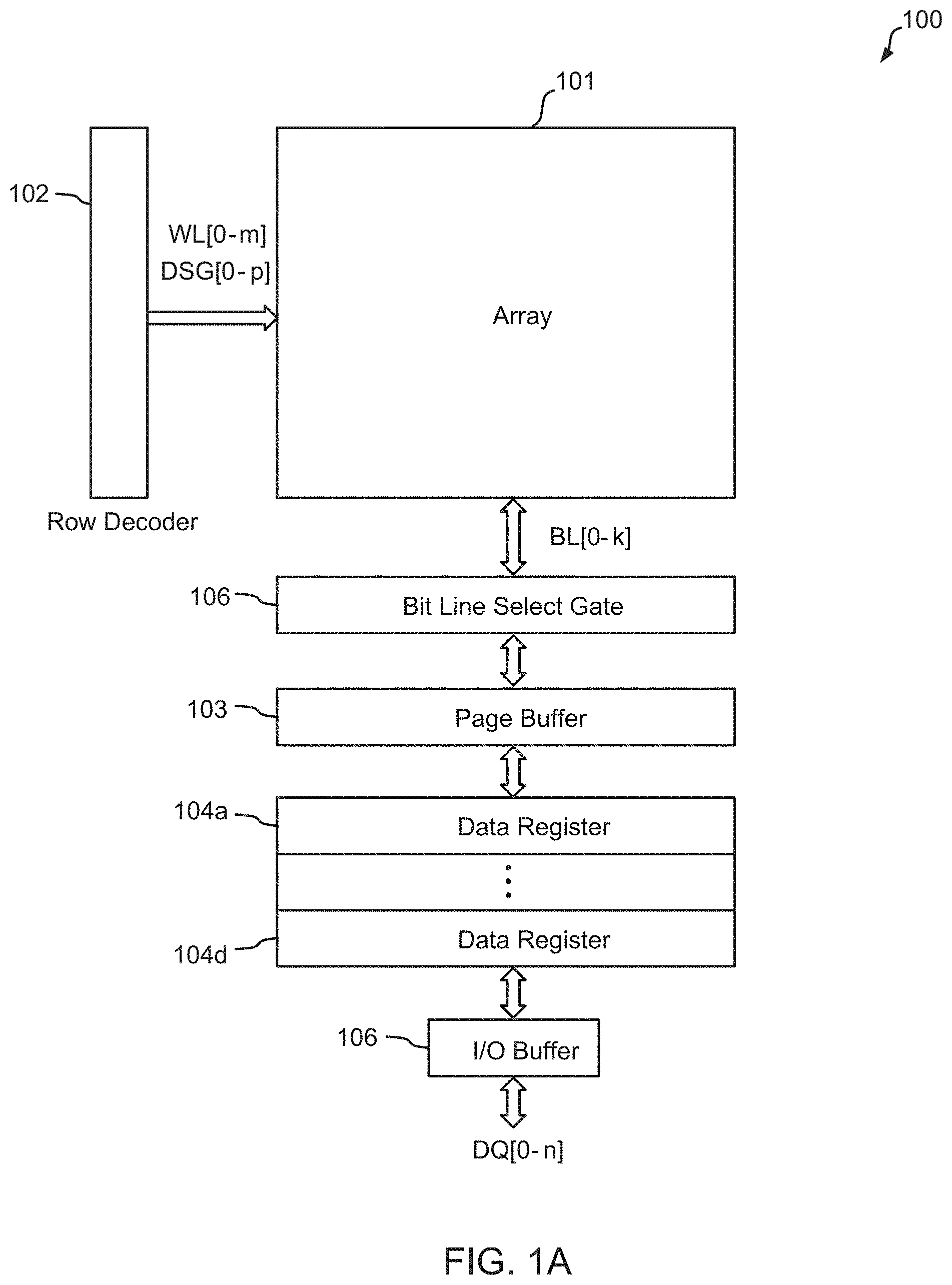
[0050] FIG. 1A shows an exemplary block diagram of NAND flash memory architecture 100 in accordance with embodiments of the invention. The architecture 100 includes a 2D or 3D NAND flash memory array 101 that that can be accessed using multiple word lines (WL[0-m]), and bit lines (BL[0-k]). The architecture 100 includes row decoder 102 and page buffer 103. The page buffer 103 contains multiple page buffers, such as page buffers 200 shown in FIG. 2A and FIG. 3A. The page buffer 103 performs both functions of a program buffer for program operations and a sense amplifier for read operations. In a conventional NAND flash memory, each page buffer is connected to one-bit line, which is referred to as an all bit line (ABL) structure, or two-bit lines, which is referred to as a half bit line (HBL) structure. In either case, the number of the bit lines that can be program and read together is equal to the number of page buffers. This is referred to as `page-programming` or `page-read`. Increasing the number of page buffers may increase the data read/write throughput, to enhance the memory performance. However, the page buffer's circuit size is quite large. It typically occupies about 20% of the die size. Therefore, the typical number of page buffers is limited to a range of 16 KB to 64 KB, which limits the read/write performance of the NAND flash memory.
[0051] In an exemplary embodiment, the architecture 100 comprises a bit line select gate block 106. The bit line select gate block 106 contains multiple bit line select gates, such as select gate 210 shown in FIG. 2A and FIG. 2B. The bit line select gates allows a page buffer to be coupled to multiple bit lines. By using a novel architecture disclosed, multiple bit lines may be programmed and read together. This is called `multiple-page programming` and `multiple-page read`. This can significantly increase the data read/write throughput without increasing the number of page buffers.
[0052] In an embodiment, data registers 104a-d are provided and may also be referred to as data cache. Although four data registers are shown, there can be any desired number of data registers. The data registers allow for parallelism between the operations of the array 101 and the data input/output (I/O). During operation, when the array 101 performs a read or write operation using the page buffer 103, the new data may be loaded into the data registers 104a-d or output from the data registers. This can enhance the performance of the memory. In an embodiment, the architecture 100 includes an input/output (I/O) buffer 106 that connects to an external data bus DQ[0-n].
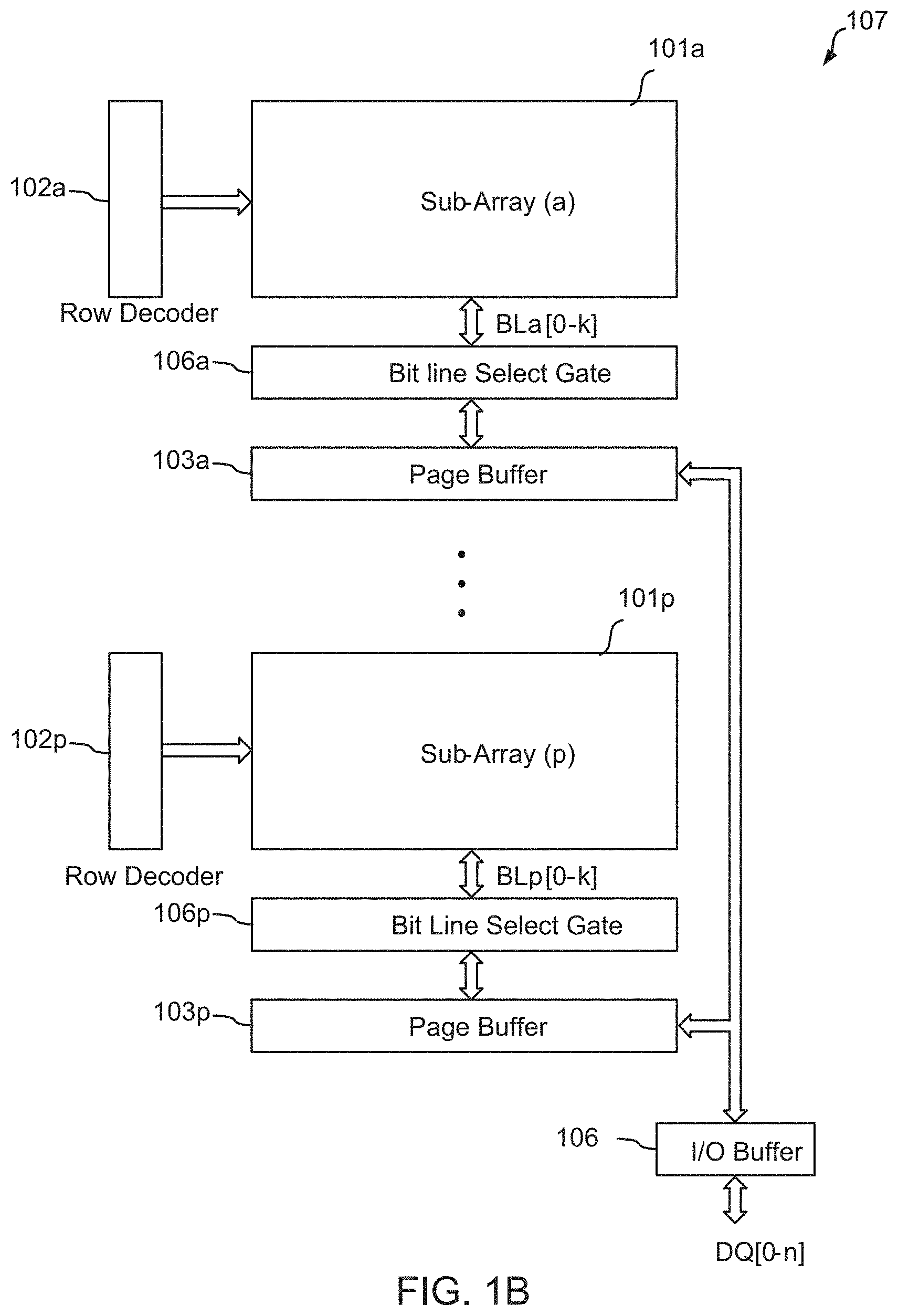
[0053] FIG. 1B shows another embodiment of a NAND flash memory architecture 107 constructed in accordance with embodiments of the invention. In this embodiment, the array is divided into multiple sub-arrays 101a to 101p. Each sub-array has its own row decoders 102a to 102p, bit line select gates 106a to 106p, and page buffers 103a to 103p. In an embodiment, each sub-array has the same number of bit lines as the array 101 shown in FIG. 1A, such as BLa[0-k] for sub-array 101a and BLp[0-k] for sub-array 101p. In an embodiment, the total number of the page buffers is the same as the embodiment shown in FIG. 1A to keep the die size the same. Assuming that the number of the sub-arrays is P, the number of the page buffers 103a to 103p for each sub-array 101a to 101p will be reduced to 1/P. As a result, the number of the bit lines connected to each page buffer is increased P times.
[0054] FIG. 1C shows a detailed embodiment of a conventional 3D NAND flash memory cell array 101 and page buffers 103. The array main contain bit lines BL[0-K]. Each bit line is connected to one of the page buffers 200a to 200k.
[0055] FIG. 1D shows a configuration of the conventional structure of a 3D NAND memory array. The 3D memory cell array 101 is located on top of the page buffer circuits 103 to save silicon area.
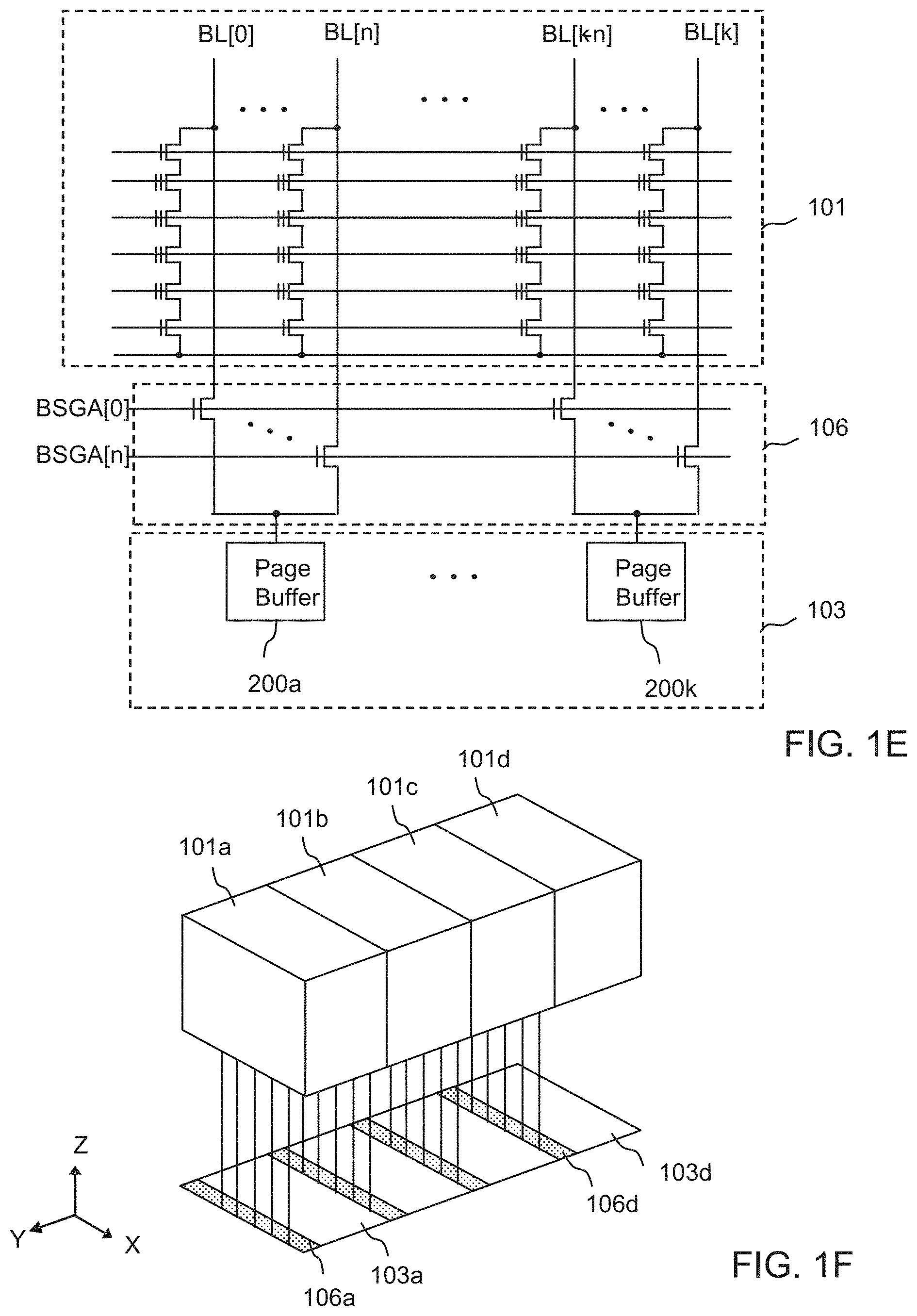
[0056] FIG. 1E shows an embodiment of an array structure in accordance with the invention. The bit lines BL[0-k] are connected to the page buffers 103 through bit line select gates 106. Therefore, the number of the page buffers 103 can be reduced when compared to a conventional architecture. For example, two bit-lines are connected to each page buffer, which reduces the number of page buffers that are used.
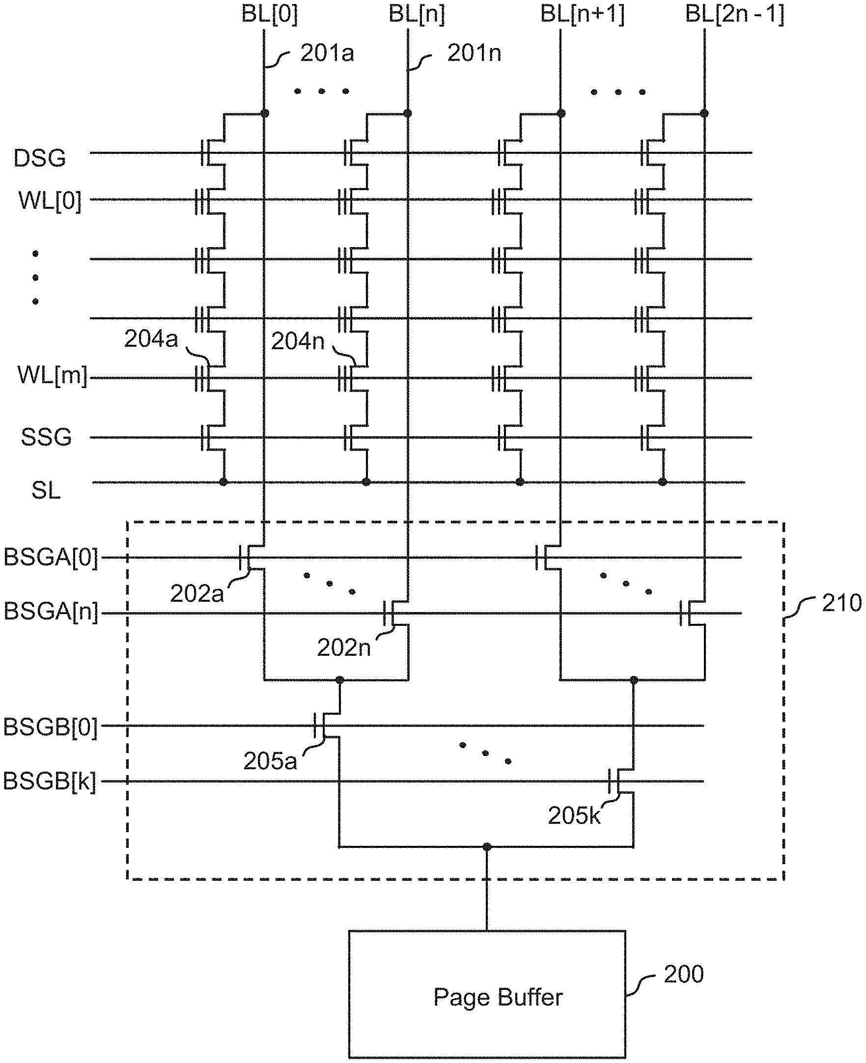
[0057] FIG. 1F shows an embodiment of a 3D array structure in accordance with the invention. The 3D cell array is divided into sub-arrays 101a to 101d that are located on top of the page buffers 103a to 103d. The sub-arrays 101a to 101d are accessed through the bit line select gates 106a to 106d. Each sub-array is connected to one page buffer.
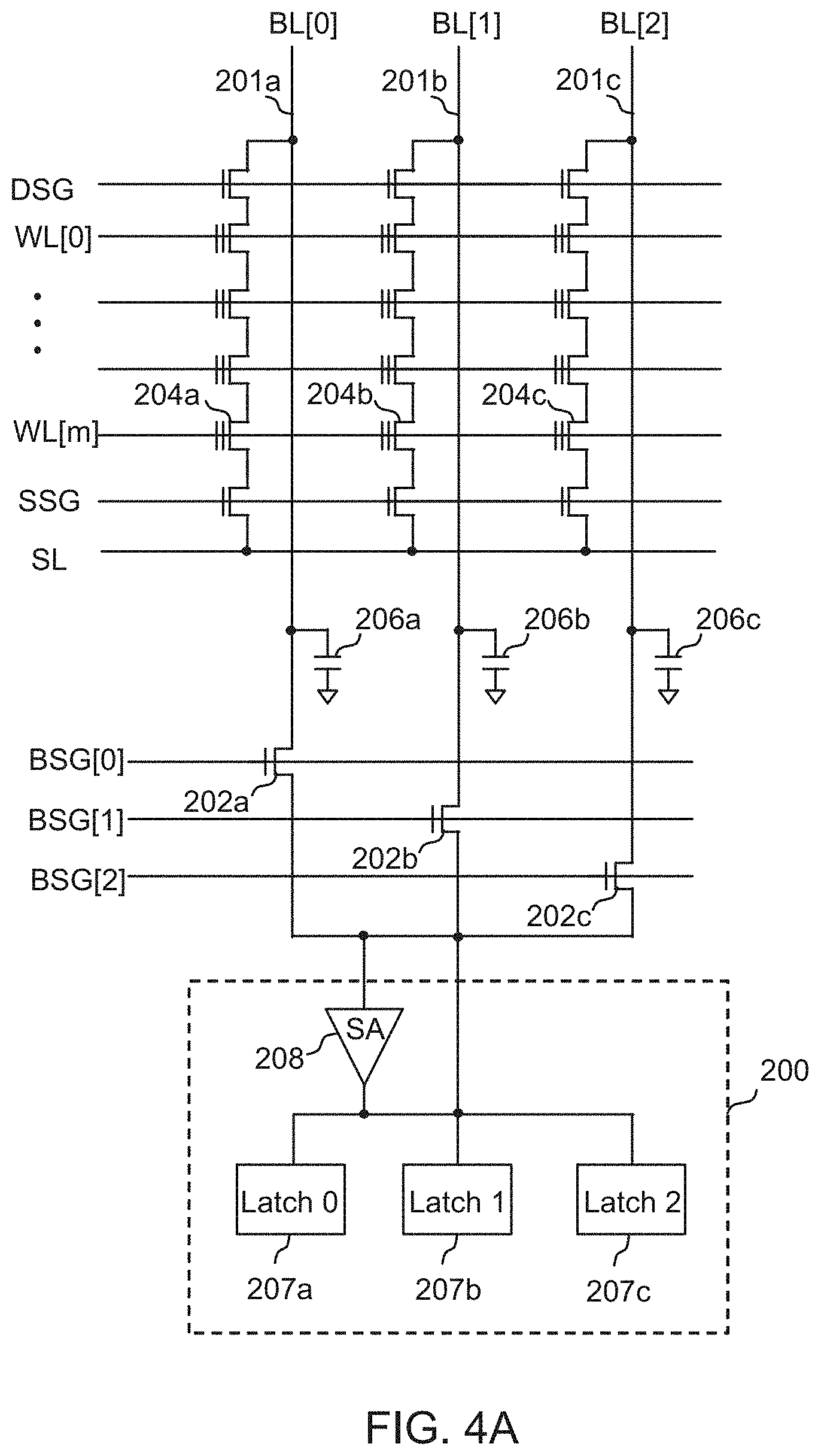
[0058] FIG. 2A shows an embodiment of a page buffer and bit line select gate configuration in accordance with embodiments of the invention. The bit lines 201a to 201n are multiple bit lines BL[0] to BL[n] in an array or sub-array. The bit line may contain multiple strings of NAND flash memory cells such as strings 211a to 211n. The strings may be formed using 2D or 3D array architectures. The bit lines are connected to a page buffer 200 through a bit line select gates 210 that comprises individual select gates 202a to 202n. Each of the bit line select gates 202a to 202n may be selected by select gate signals BSG[0] to BSG[n]. The number of the bit lines connected to one page buffer may be any number, such as 2, 4, 8, 16, etc. There is no limitation for the number of the bit lines that can be connected to one page buffer.
[0059] The page buffer 200 functions as both a program buffer and a sense amplifier. The page buffer 200 contains multiple latches 207a to 207n to store program data. A sense amplifier 208 operates to read the data from the cells. In program mode, the latches 207a to 207n apply the program data to the bit lines. In program-verify mode, the sense amplifier 208 reads the data from the cells, and updates the program data stored in the latches 207a to 207n. In read mode, the sense amplifier 208 reads the data from the cells and stored in the latches 207a to 207b, and then the data may be transferred to an output buffer.
[0060] In conventional systems during programming, one page buffer may only provide one data value to one bit line at one time. During read and program-verification, one page buffer may only read data from one bit line at one time. Therefore, the total bit lines in programming, verification, and read are equal to the number of page buffers. For example, in one conventional system, each bit line is connected to one page buffer. This is called an All Bit Line (ABL) architecture. In another conventional design, two bit lines are shared with one page buffer. This architecture is referred to as a Half Bit Line (HBL) architecture. This architecture reduces by half number of the page buffers. However, during read and write mode, only half of the bit lines may be connected to the page buffers, and therefore the data throughput is reduced by 1/2.
[0061] In various exemplary embodiments, a novel architecture is disclosed to read and write multiple bit lines with one page buffer simultaneously, and therefore the data throughput may be significantly increased. For example, in FIG. 2A, assuming the word line WL[m] is selected, the cells 204a to 204n may be read and programmed simultaneously by one page buffer 200. Thus, the number of the page buffers may be reduced and the read and write data throughput may be increased. A more detailed description of the design and operation of the novel NAND flash memory architecture is provided below.
[0062] It should also be noted that the cells 204a to 204n may belong to different pages. The pages may be selected by the bit line select gate signals BSG[0] to BSG[n]. Therefore, the architecture may provide multiple bit-line read and write operations, or multiple-page read and write operations.
[0063] In traditional page buffer design, the number of the latches in a page buffer is determined by the number of bits stored in one cell. For example, for an SLC design, the page buffer may have only one latch to store 1-bit of data. For MLC design, the page buffer may have two latches to store 2-bits of data. For TLC, the page buffer may have 3 latches to store 3-bits of data. For QLC, the page buffer may have 4 latches to store 4-bits of data. However, in accordance with embodiments of the invention, extra latches may be added to further enhance the advantages of the multiple-page read and write operations.
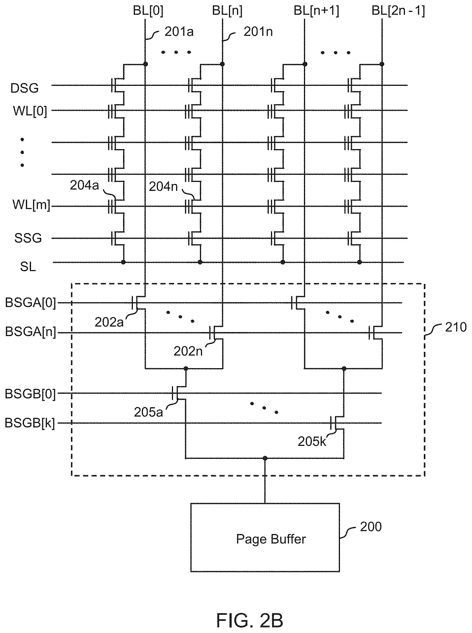
[0064] FIG. 2B shows another embodiment of the page buffer configuration in accordance with embodiments of the invention. As illustrated in FIG. 2B, the array may have multiple layers of bit line select gates, such as 202a to 202n and 205a to 205k. In this case, the select gates 202a to 202n are the first layer of bit line select gates that are connected to control signals BSGA[0] to BSGA[n]. The select gates 205a to 205k are the second layer of bit line select gates that are connected to control signals BSGB[0] to BSGB[k]. Compared with the embodiment shown in FIG. 2A, this embodiment reduces the number of control signals. For example, assuming 16 bit lines share one page buffer, the embodiment in FIG. 2A uses 16 control signals, while the embodiment in FIG. 2B uses 8 control signal, (e.g., 4 for the first layer and 4 for the second layer). In various embodiments, there is no limitation on the number of the layers of bit line select gates. For example, the array may have 2, 3, 4, etc. layers of bit line select gates. In an embodiment, the bit line select gates may be implemented using any suitable devices. They are not limited only to NMOS devices.
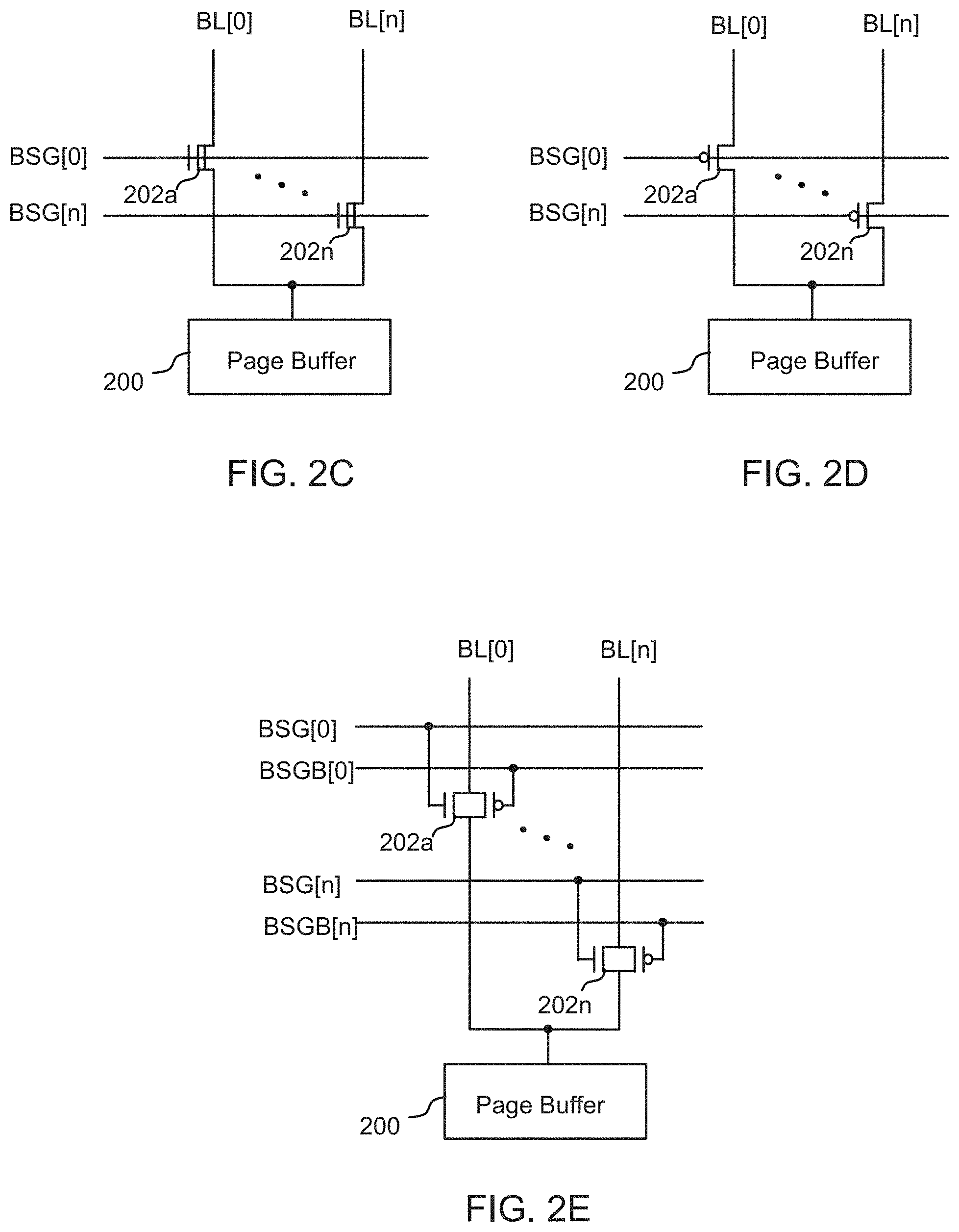
[0065] FIGS. 2C-E show embodiments illustrating bit line select gates in accordance with the invention.
[0066] FIG. 2C shows a circuit that illustrates how the bit line select gates 202a to 202n may be implemented by native devices or depletion-mode devices to increase the bit line pre-charged voltage and current.
[0067] FIG. 2D shows a circuit that illustrates how the bit line select gates 202a to 202n may be implemented by PMOS devices.
[0068] FIG. 2E shows a circuit that illustrates how the bit line select gates 202a to 202n may be implemented by PMOS-NMOS pairs. Moreover, the bit line select gates may be implemented by high voltage (HV) devices or low voltage (LV) devices. These modifications and variations are within the scope of the embodiments.
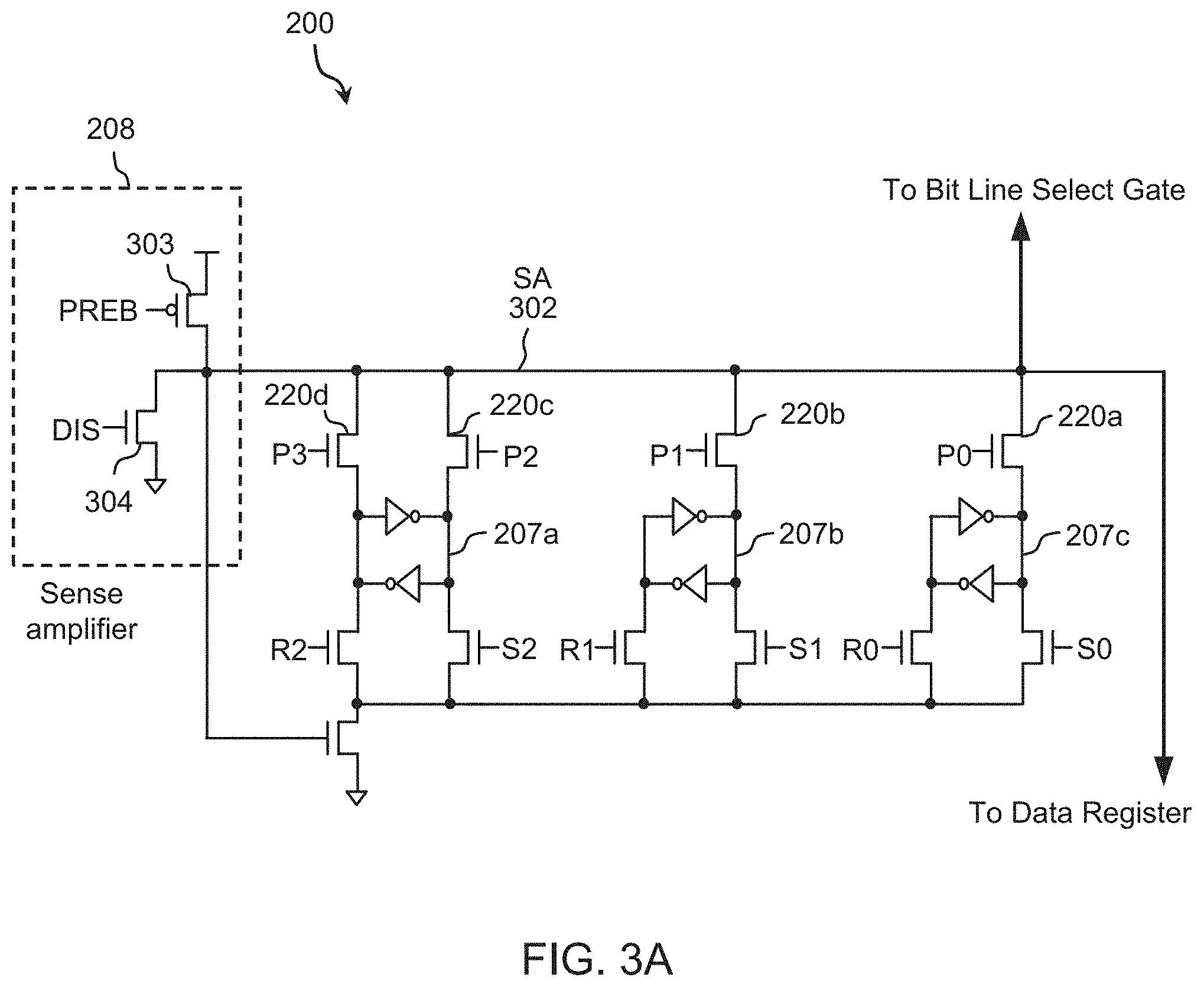
[0069] FIG. 3A shows an embodiment of the page buffer circuit 200. The page buffer 200 circuit is configured both as a program buffer and a sense amplifier. The program buffer comprises three latches 207a to 207c. Latch pass gates 220a to 220d are also shown. During program mode, 3 bits of data, D2, D1, and D0, are first loaded into the three latches 207a to 207c. The signals P0 to P3 select and turn on one of the pass gates 220a to 220d to pass the data of the latches 207a to 207c to the selected bit line according to the programmed Vt level to program the selected cell. Also shown is sense amplifier 208.
[0070] During read mode, the data may be read from the cells by the sense amplifier 208, and then latched in the three latches 207a to 207c. A Sense Amplifier's sensing node 302 is denoted by (SA). The sense amplifier 208 includes a pre-charge device 303 and a discharge device 304. The detailed operation of the operation of the sense amplifier 208 is described below with reference to FIGS. 6A-C.
[0071] FIG. 3B shows another embodiment of the page buffer circuit 200. The page buffer 200 shown in FIG. 3B is used for current-sensing, while the embodiment shown in FIG. 3A is used for voltage-sensing. In this embodiment, a gain stage, such as comparator 305, is added to the sense amplifier 208 to amplify the voltage of sensing node 302. In another embodiment, the comparator 305 is replaced by invertor. Moreover, a bias device 306 may be added to become a cascade stage. The bias device 306 limits the bit line's pre-charge voltage to (BIAS-Vt) rather than VDD, thus it reduces the pre-charging time.
[0072] FIGS. 4A-D show the operation of the page buffer and bit line select gates in accordance with the invention.
[0073] FIG. 4A shows an exemplary embodiment that uses a TLC page buffer 200. The TLC page buffer 200 comprises three data latches 207a to 207c and a sense amplifier 208. For embodiments using MLC and QLC, the page buffer may contain two and four data latches, respectively. The page buffer 200 is connected to multiple bite lines 201a to 201c through the bit line select gates 202a to 202c. Bit line capacitances 206a to 206c represents the bit line capacitance of the bit lines 201a to 201c, respectively.
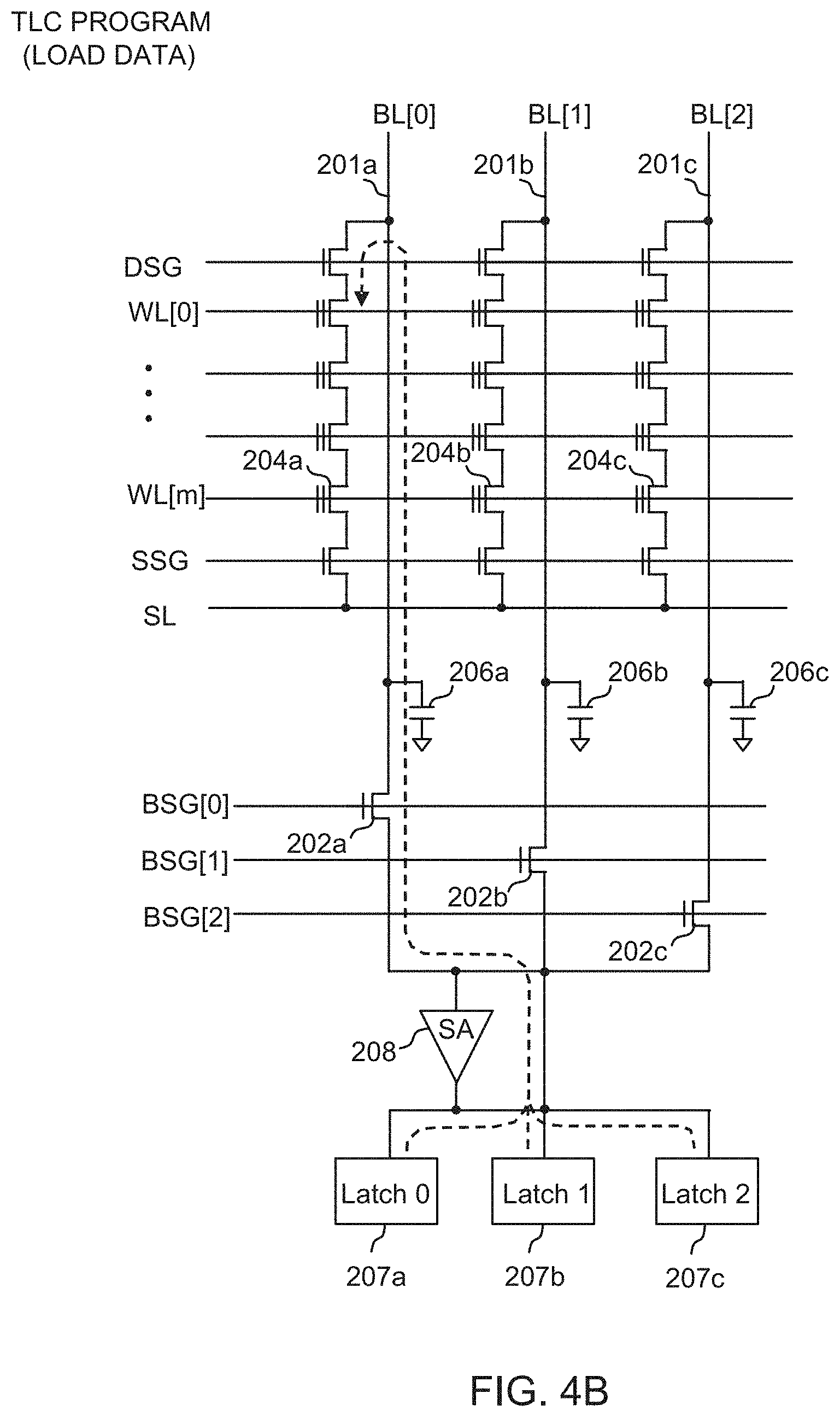
[0074] FIG. 4B illustrates basic TLC program operations. The TLC programming operations program three bits of data into one selected cell. The TLC programming may contain multiple program steps to program the cell from the erased Vt into eight Vt levels to represent the three bits of data. Assume that the cell 204a is selected. In each program step, one of the data latches 207a to 207c may be selected to load data to the selected bit line 201a to program the cell 204a, depending on which Vt level is programed. For example, when programming the D0 bit, the data stored in the Latch 0 207a is loaded to the selected bit line 201a to program the selected cell 204a. When programming the D1 bit, the data stored in the Latch 1 207b may be loaded to the selected bit line 201a to program the selected cell 204a. When programming the D2 bit, the data stored in the Latch 2 207c may be loaded to the selected bit line 201a to program the selected cell 204a, etc. In this operation, the number of cells being programmed equals to the number of page buffers. Therefore, it is referred as `single-page programming`.
[0075] FIG. 4C shows multiple-page programing operations in accordance with the invention. In an embodiment, the data stored in the latches 207a to 207c are programmed to multiple cells 204a to 204c on multiple bit lines 201a to 201c simultaneously. If the page buffer has N data latches, it may program N cells simultaneously. This significantly increases the program data throughput N times.
[0076] To load the multiple-page data, the bit line select gates 202a to 202c may be sequentially turned on to load the data from the latches 207a to 207c to the bit lines 201a to 201c, respectively, as shown by the arrowed lines. After the data is loaded to the bit lines 201a to 201c, the bit line select gates 202a to 202c are turned off, then the data is held by the bit line capacitance 206a to 206c. After that, a program condition is applied to the selected word line, WL[m], to program the selected cells 204a to 204c according to the data stored in the bit line capacitance 206a to 206c. By using these operations, the data of the multiple bit lines may be programmed simultaneously.
[0077] In an exemplary embodiment, the page buffer performs two programming function modes. One is TLC programming and the other is SLC programming. When the page buffer performs TLC programing, the data latches 207a to 207c are used to store three bits data, D0, D1, and D2 for one cell, and the three data bits are programmed into a single cell. In SLC programming, the three data latches may be used to store three single-bit data, and then this data is programmed into three cells. This is referred as `multiple-page programming`.
[0078] By using the above-described multiple-page SLC programming, the data throughput may be significantly increased. Therefore, this mode may be used to program the data into the cells at high speed. Later in idle time, the data may be read out from the SLC cells and re-programmed to other cells using TLC mode, and then the SLC cells may be erased to increase the storage capacity of the memory.
[0079] The disclosed multiple-page programming operations may be applied not only to SLC, but also to multiple level cells such as MLC, TLC, and QLC, etc. For example, referring to FIG. 4C, assume three pages' data is programmed into the selected cells 204a to 204c using TLC mode. Each cell may store one of eight Vt levels to represent three data bits, D0, D1, and D2. In the first step, the first page's data is loaded into the data latches 207a to 207c. Then, the data are sequentially loaded to the bit lines 201a to 201c using the previously described operation, and then the program condition is applied to the cells 204a to 204c to program each cell according to the bit line data. The cells will be programmed to the Vt levels corresponding to D0 bit. A program-verify operation may be performed to check the cells' Vt. The program-verify operation will be described later in reference to FIGS. 6A-C. After the data is successfully programmed, the data in the latches 207a to 207c may be cleared.
[0080] In the second step, the second page's data is loaded into the three latches 207a to 207c, then sequentially loaded to the bit lines 201a to 201c to program the cells 204a to 204c to the Vt levels corresponding to D1 bit. After the second page's data is successfully programmed, the data in the latches 207a to 207c may be cleared. In the third step, the third page's data is loaded to the latches 207a to 207c, and then applied to the bit lines 201a to 201c to program the cells 204a to 204c to the Vt levels corresponding to D2 bit. By repeating the sequence, the cells may be programmed to any number of multiple-level cells such as MLC, TLC, QLC, etc.
[0081] FIG. 4D shows another exemplary programming embodiment in accordance with the invention. Assuming the chip has multiple data registers 212a to 212c. Each data register contains multiple-bit latches such as Reg 0 to Reg 2. During SLC programming mode, the data of the first data register 212a is loaded to the latches 207a to 207c, and then loaded to the bit lines 201a to 201c to program the cells 204a to 204c, respectively. After the data is successfully programmed, the data of the next register 212b may be loaded to the latches 207a to 207c, and then loaded to the bit lines 201a to 201c to program another page such as cells 214a to 214b, respectively. In this way, the multiple pages' data can be programmed simultaneously to increase program data throughput.
[0082] For the TLC programming mode, the data stored in the first data register 212a may be transferred to the latches 207a to 207c, and then programmed to the Vt levels corresponding to D0 bit of the selected cells 204a to 204c. Then, the data stored in the second data register 212b may be transferred to the latched 207a to 207c, and then programmed to the Vt levels corresponding to the D1 bit of the selected cells 204a to 204c. The operation may be repeated to program the data of the third data register 212c to the D2 bit of the selected cells 204a to 204c.
[0083] In an embodiment, the data in the data registers 212a to 212c may be programmed to the cells in any suitable orders. For example, in another embodiment, in the first step, the data stored in the Reg 0 of the data registers 212a to 212c may be sequentially transferred to the data latch 207a, then loaded to the bit lines 201a to 201c, and then programmed to the Vt level for the D0 bit of the cells 204a to 204c. In the second step, the data stored in the Reg 1 of the data registers 212a to 212c may be sequentially transferred to the data latch 207b, then loaded to the bit lines 201a to 201c, and then programmed to the Vt level for the D1 bit in the cells 204a to 204c. In the third step, the data stored in the Reg 2 of the data registers 212a to 212c may be sequentially transferred to the data latch 207c, then loaded to the bit lines 201a to 201c, and then programmed to the Vt level for the D2 bit in the cells 204a to 204c.
[0084] FIG. 5A shows exemplary waveforms for multiple-page programming of the circuit as shown in FIG. 4C. Referring now to both FIG. 4C and FIG. 5A, at time T1, BSG[0] to BSG[2] may go high to turn on the bit line select gates 202a to 202c. Assume the page buffer's output data is called PB. The page buffer (PB) may apply VDD to all the bit lines BL[0] to BL[2]. The selected cell strings' drain select gate (DSG) is supplied with VDD. The source select gate (SSG) is supplied with 0V. Therefore, the channel region of the strings STRG[0] to STRG[2] may be charged to VDD-Vt of the drain select gate.
[0085] At time T2, the selected word line, WL[m], and the other unselected word lines are applied with the program voltage, such as 20V, and an inhibit voltage such as 10V, respectively. The word lines' voltage may couple the channel region of all the strings STRG[0] to STRG[2] to a voltage of about 8V. This voltage may inhibit the programming of the cells. Due to the bit lines being supplied with VDD, the drain select gates are reverse-biased. Thus, the drain select gates will be turned off to prevent the channel voltage from leaking to the bit lines.
[0086] At time T3, the bit line select gates BSG[0] to BSG[2] are turned off. The bit line capacitance, such as 206a to 206c shown in FIG. 4C, holds the bit lines' voltage at VDD.
[0087] At time T4, the first bit line select gate BSG[0] is turned on, and the page buffer (PB) applies the first data to the first bit line BL[0]. If the data is `1` (VDD), the channel of the string STRG[0] will remain at the inhibit voltage such as 8V. If the data is `0` (0V), it will turn on the drain select gate and discharge the string STRG[0] to 0V. This will cause the first selected cell 204a to be programmed. After the first bit line select gate BSG[0] is turned off at T5 time, the bit line BL[0] and the string STRG[0] may remain at 0V due to the bit line capacitance 206a.
[0088] The steps may be repeated to sequentially turn on the bit line select gates BSG[1] to BSG[2] to load the data from the page buffer (PB) to bit lines BL[1] and BL[2] and their strings STRG[1] and STRG[2].
[0089] After all the data is loaded, at time T6, a timer may start to count the program pulse, Tpgm, over a time interval from 10 us to 30 us. Then, the program pulse is ended. By using the above processes, multiple bit lines may be loaded with different data and programmed simultaneously.
[0090] It should be noted that the waveform of FIG. 5A is for illustration and not drawn on scale. In reality, the total program time is dominated by Tpgm. The data loading time may be negligible. Therefore, the multiple-page programming may significantly reduce the total programming time and increase the program data throughput.
[0091] FIG. 5B shows another embodiment of waveforms for multiple-page programming in accordance with the invention. These waveforms are similar to the waveforms shown in FIG. 5A except that the bit line select gates BSG[0] to BSG[2] may be turned off (as illustrated at 506) after pre-charging the bit lines to VDD at time T1. Therefore, the bit lines' voltage is held by the bit line capacitance.
[0092] FIG. 5C shows another embodiment of waveforms for multiple-page programming in accordance with the invention. These waveforms are similar to FIG. 5A except that the drain select gate (DSG) of the selected string may be turned off after the data is loaded to the multiple bit line (as illustrated at 508) at T6 time. In this way, if the floating bit lines have leakage, the bit line voltage needs to be drop from VDD to lower than Vt of the drain select gate to turn on the drain select gate. Therefore, this approach provides a higher margin of failure for the string's inhibit voltage.
[0093] FIG. 5D shows another embodiment of waveforms for multiple-page programming wherein the operations shown in FIG. 5C are applied to the waveforms shown in FIG. 5B to produce the waveforms shown in FIG. 5D. In an embodiment, the selected string's drain select gate (DSG) is turned off after the strings are pre-charged (as illustrated at 510) at T1 time. The DSG can be turned on (as illustrated at 512) at T3 time to load the multiple pages' data into the stings, and then turned off (as illustrated at 514) at T6 time to increase the floating bit lines' leakage margin.
[0094] FIG. 5E shows another embodiment of waveforms for multiple-page programming in accordance with the invention. At time T1, the selected drain select gate (DSG) is turned on, and the source select gate (SSG) is off. From T1 to T2 time, the page buffer (PB) supplies multiple-page data, Data 0, Data 1 and Data 2. The bit line select gates BSG[0] to BSG[2] are turned on sequentially to load the data into BL[0] to BL[2] and STRG[0] to STRG[2]. At time T3, the selected word line and unselected word lines are supplied with the program voltage 20V and the inhibit voltage 10V, respectively. The word lines' voltage will couple the channel region of STRG[0] to STRG[2] with data value of `1` to a voltage about 8V, to inhibit the programming of the cells. For the strings storing a data value of `0` (0V), the drain select gate is on, thus it will cause charge-sharing between the string's capacitance and the bit line capacitance. Since the bit line capacitance is much higher than the string's capacitance, as a result, the string's voltage is very closed to 0V. This will cause the selected cell to be programmed.
[0095] In an embodiment, the circuit shown in FIG. 2A allows multiple-page cells to be program-verified and read simultaneously by using the page buffer 200.
[0096] FIGS. 6A-C show multiple-page read operations in accordance with embodiments of the invention. In an embodiment, the multiple-page read operations comprise three steps. The three steps are pre-charging the bit line, discharging the bit line, and sensing.
[0097] FIG. 6A shows an exemplary circuit that performs the pre-charge bit line step. During operation all the bit line select gates 202a to 202c are turned on, and a pre-charge device, such as device 303 in the sense amplifier 208 as shown in FIG. 3A, is turned on to pre-charge the bit line capacitances 206a to 206c to a pre-charge voltage such as VDD, for example, as shown by the dashed lines.
[0098] FIG. 6B shows an exemplary circuit that performs the discharge bit line step. During operation, the bit line select gates 201a to 202c are turned off. The read bias conditions are applied to the selected cells 204a to 204c. The selected word line such as WL[m] is supplied with a read voltage to turn on or off the cells 204a to 204c according to the cells' Vt. The on-cells will discharge the bit lines simultaneously. It will be assumed that the cells 204a and 204b are an on-cell and an off-cell, respectively. The on-cell 204a will discharge the bit line capacitance 206a to 0V. The off-cell 204b will not discharge the bit line, and thus the bit line capacitance 206b will remain at the pre-charged voltage. Since the on-cell current is very low (e.g., only about 1 uA), and the bit line capacitance is high due to its connection to many strings, this bit line discharging step may take about 25 us to 35 us. Thus, the read time is dominated by the bit line discharging time. Thus, by using multiple bit lines discharging according to the invention, the total read time is reduced and the read data throughput is significantly increased.
[0099] FIG. 6C shows an exemplary circuit that performs the sensing step. In this step, the bit line select gates 202a to 202c are sequentially turned on to allow the data stored by the bit line capacitance 206a to 206c to be sensed by the sense amplifier 208 of the page buffer, as shown by the dashed lines. When a bit line select gate is turned on, it will cause charge-sharing between the bit line capacitance and the sensing node 302 of the page buffer circuit as shown in FIG. 3A. Because the capacitance of the sensing node 302 is much lower than the bit line capacitance, the sensing node 302 will be pull up or down in very short time. Therefore, each bit line's data may be read in very short time.
[0100] After the data is stored in the data latches 207a to 207c, the data may be transferred to the data register, and then the data register may start to output the data. Meanwhile, the page buffer may start to read the next page's data from the cells. If the chip does not have data register, the data may be output directly from the data latches of the page buffer, and then the page buffer may start to read the next page's data from the cells.
[0101] In an embodiment, the operations illustrated in FIGS. 6A-C may be also used for multiple-page program-verification. The program-verify operation is very similar to the read operation. The only differences are the word line voltage and the data latches' operation. In read mode, the data read from the cells are stored in the data latches directly. In program-verify mode, the data read from the cells are used to update the data in the data latches.
[0102] Referring to FIG. 6B, for program-verify condition the selected word line may be supplied with a program-verify voltage instead of a read voltage in order to check the cells' Vt. In FIG. 6C, after the cells' data is read by the sense amplifier 208, the data will be used to update the data stored in the latches 207a to 207c for the next program pulse. The logic operation of updating the latches is well known, thus it is not described here.
[0103] FIG. 6D shows another exemplary embodiment of a circuit in accordance with the invention. In this embodiment, the chip contains multiple data registers 212a to 212n. Also shown are strings of NAND flash memory cells 211a to 211f and bit line select gates 202a to 202f. During operation, the data of first data register 212a may be loaded to bit lines 201a to 201c to program the first group of strings 215a, and the data of the second data register 212n may be loaded to bit lines 201d to 201f to program the second group of strings 215b.
[0104] FIG. 7A shows an embodiment of read operation waveforms in accordance with the invention. At time T1, a selected word line is supplied with a read voltage, Vread, and the unselected word lines are supplied with a pass voltage, Vpass. The drain select gate (DSG) and the source select gate (SSG) are turned on. The source line (SL) is supplied with 0V. These conditions turn on on-cells and turn off off-cells.
[0105] At time T2, the bit line select gates BSG[0] to BSG[2] are turned on and a pre-charge signal PREB, as shown in the page buffer circuit in FIG. 3A, is activated to pre-charge BL[0] to BL[2] to VDD-Vt (of the bit line select gate) or a pre-determined voltage.
[0106] At time T3, the bit line select gates BSG[0] to BSG[2] are turned off. The bit lines BL[0] to BL[2] will become floating and the selected cells will start to discharge the bit lines. For on-cells, the cell will conduct current to discharge the cell string and the bit line to 0V. For off-cells, the bit line will remain at the pre-charged voltage due to the cell being turned off.
[0107] Because the on-cell current is very low, which may be only 1 uA to 5 uA, and the bit line capacitance is large, it may take long time to discharge the bit line. A time to discharge the bit line is in a range of about 25 us to 35 us. As a result, the bit line discharge time, shown Tdis, may dominate the entire read time. However, in accordance with the invention, all the BL[0] to BL[2] are discharged simultaneously, thus the total read time is significantly reduced.
[0108] After a pre-determined discharge time, Tdis, at time T4, the first bit line select gate BSG[0] may be turned on. This causes charge-sharing to occur between the sensing node (SA) and BL[0]. Because BL[0] has much higher capacitance than the Sense Amplifier's sensing node (SA), the sensing node (SA) may be charged to almost VDD or discharged to almost 0V in very short time. Then, a first latch signal LAT[0] may be activated to latch the data to the data latch of the page buffer. After the data is latched, the BSG[0] may be turn off to isolate BL[0] from the sensing node (SA).
[0109] At time T5, the pre-charge signal PREB is activated to pre-charge the sensing node (SA) to VDD. Then, the second bit line select gate BSG[1] is turned on to read the data of the second bit line BL[1]. The steps from T4 to T5 are repeated to read the data from next bit line until all bit lines are read.
[0110] If the chip does not have data register, after the data is latched in to the page buffer, the data may be output from the page buffer directly, and then the steps from T4 to T5 may be repeated to read the data from the next bit line. If the chip has data registers as shown at 104a to 104d in FIG. 1A, the data may be transferred from the page buffer to the data register. Thus, the data register may output the data to the I/O buffer while the next bit line's data is read by the page buffer.
[0111] In this embodiment, the multiple bit lines may be read by using only one page buffer circuit. Since the bit lines BL[0] to BL[2] are discharged simultaneously, the total read time and the read data throughput are similar to the traditional art that uses the All Bit Line (ABL) architecture.
[0112] The waveforms shown in FIG. 7A are for reading one Vt level. For multiple level cells such as MLC, TLC, and QLC, the waveforms may be repeated multiple times with different selected word line voltages to read the multiple bits of the selected cells.
[0113] The waveforms shown in FIG. 7A demonstrate the fundamental concepts of the embodiments. The waveforms may be modified according to many design considerations or requirements. For example, in another embodiment, the word lines' voltage may be applied after T3 instead of at T1. These modifications and variations shall remain in the scope of the embodiments.
[0114] FIG. 7B shows another embodiment of read operation waveforms in accordance with the invention. This embodiment is similar to the embodiment shown in FIG. 7A except that at time T1, the source line (SL) is supplied with a positive voltage such as VDD.
[0115] At time T2, a discharge signal (DIS), as shown in the page buffer circuit in FIG. 3A, is activated to discharge the sensing node (SA) and the bit lines BL[0] to BL[2] to 0V.
[0116] At time T3, the bit line select gates BSG[0] to BSG[2] are turned off, and thus the bit lines BL[0] to BL[n] become floating. The on-cells may start to charge up the bit lines. The bit line may be charged to Vread-Vt (of on-cells).
[0117] At time T4, a pre-charge signal PREB is activated to pre-charge the sensing node (SA) to VDD. Then, the bit line select gate BSG[0] is turned on. The voltage of BSG[0] may not be higher than the bit line voltage +Vt (of the bit line select gate). Therefore, for on-cells, the bit line select gate will be turned off. The sensing node (SA) will remain at VDD. For off-cells, because the BL remains at 0V, the bit line select gate will be turned on. The sensing node (SA) will be discharged to almost 0V due to the charge-sharing between the bit line and the sensing node. Then, a latch signal LAT is activated to latch the data of the sensing node in the page buffer. Then, the steps from times T4 to T5 may be repeated to read the data from the next bit line.
[0118] FIG. 7C shows another embodiment of read operation waveforms in accordance with the invention. This embodiment uses current-sensing operations. For example, the page buffer circuit shown in FIG. 3B may be used to perform current-sensing. The operations shown in FIG. 7C are similar to those shown in FIG. 7A except that at time T1, the pre-charge signal PREB is activate to pre-charge the sensing node (SA) and bit lines BL[0] to BL[2]. A BIAS voltage is applied to the bias device 306 shown in FIG. 3B to limit the bit line pre-charge voltage to Vbias-Vt (of the bias device). The bit line discharge time between times T3 and T4 is much shorter, because current-sensing does not require the bit line voltage to discharge to near 0V. It only needs to discharge the bit line voltage to lower than Vbias-Vt to turn on the bias device. At time T4, the pre-charge signal PREB is supplied with a reference voltage, Vref, to limit the pull-up current of the pre-charge device 303 shown in FIG. 3B. The pull-up current is lower than the on-cells' current. Thus, for on-cells, the sensing node (SA) may be discharged to the same bit line voltage as the on-cells' voltage. For off-cells, the sensing node (SA) remains at VDD. As a result, the gain stage of the comparator 305 amplifies the SA voltage to full VDD and 0V. Then, the operations as described in FIG. 7A are performed.
[0119] FIG. 7D shows another embodiment of read operation waveforms in accordance with the invention that utilize current-sensing. This embodiment is similar to the embodiment shown in FIG. 7C except that the bias device 306 shown in FIG. 3B is removed. Therefore, the function of the bias device is performed by the bit line select gates 202a to 202n. During pre-charging and sensing, the bit line select gates BSG[0] to BSG[n] are supplied with a bias voltage, Vbias, as shown in FIG. 7D.
[0120] FIG. 8A shows an embodiment of program and program-verify pulses. As shown in FIG. 8A, the word line (WL) experiences a program pulse 801 and a program-verify pulse 802. The word line is supplied with a program voltage and verify voltage during these times accordingly. For program pulse 801, the data of multiple pages are loaded sequentially (as shown at 803) and then programmed simultaneously (as shown at 804). For the verify pulse 802, the bit lines of multiple pages are discharged simultaneously (as shown at 805), and then the bit lines' data is sensed sequentially (as shown at 806).
[0121] FIG. 8B shows an embodiment of a read operation. As shown in FIG. 8B, the bit lines of multiple pages are discharged simultaneously (as shown at 807), and then the bit lines' data is sensed sequentially (as shown at 808).
[0122] FIG. 8C shows an embodiment of MLC read or program-verify operations. As shown in FIG. 8C, the word line is supplied with multiple-level voltages 809a to 809c. For each level, multiple bit lines are discharged simultaneously, as shown at 801a to 801c, and sequential sensed, as shown at 811a to 811c.
[0123] FIG. 9A shows a traditional NAND flash memory array architecture. A shown in FIG. 9A, an array 901 is accessed using M word lines and N bit lines. A page buffer 902 is provided that contains the same number of buffers as the number of the bit lines.
[0124] FIG. 9B shows an embodiment of an array architecture in accordance with the invention. As shown in FIG. 9B, the array is divided into two sub-arrays 901a and 901b. Each sub-array is accessed using M/2 word lines and N bit lines. Each sub-array is connected to one of the page buffers 902a and 902b through 2-to-1 bit line select gates. Therefore, the number of the page buffers 902a and 902b each may be N/2. As a result, the number of total page buffers is N, which is the same as in the array shown in FIG. 9A. Therefore, the silicon area of the array architectures shown in FIGS. 9A-B are similar. However, as described above, the array architecture in FIG. 9B may double the read data throughput, compared with the array shown in FIG. 9A. Furthermore, the bit line length of the array architecture shown in FIG. 9B is 1/2 of the BL length of the array shown in FIG. 9A, and thus its BL capacitance is 1/2 as much. Therefore, the BL discharge time may be reduced to 1/2. Because the BL discharge time dominates the total read time, the total read time may be reduced by about 1/2. Please notice, this read time reduction may benefit both random read and sequential read operations. Moreover, the sub-arrays 901a and 901b may be read and programmed independently. This results in 2-plane operations.
[0125] FIG. 9C shows another embodiment of an array architecture that uses 4 sub-arrays 901a to 901d. Each sub-array utilizes N/4 page buffers, such as 902a to 902d. The bit lines are connected to the page buffer through 4-to-1 BL select gates, such as 903a to 903d. As a result, the total page buffer number is the same as the array shown in FIG. 9A. Thus, the silicon area of this array architecture is similar to the array shown in FIG. 9A. However, in accordance with the invention, this array has 4 times the read data throughput compared with the array of FIG. 9A. Furthermore, the bit line length becomes 1/4 for this array architecture, its bit line capacitance as well as the bit line discharge time become 1/4 as well. As a result, the read latency also becomes 1/4. Moreover, the 4 sub-arrays 901a to 901d can be read and programmed independently, resulting in 4-plane operations.
[0126] In various exemplary embodiments, the array is divided into any number of sub-arrays. The more sub-arrays, the shorter read latency, and higher data throughput may be obtained.
[0127] FIG. 9D assumed that array is divided into K sub-arrays. The read latency becomes 1/K and the data throughput become K times the array as shown in FIG. 9A. For example, typical SLC NAND flash memory read latency is about 25 us and data throughput is about 640 MB/s. Assuming the array is divided into 32 sub-arrays, the read latency may be reduced to 25 us/32=0.8 us, and the data throughout may be increased to 640 MB/s.times.32=20.5 GB/s, while the die size remains about the same. This high data throughput may saturate the I/O speed when using a low I/O pin count such as 8 or 16. Therefore, it may be most advantageous for use with products having high I/O pin counts, such as Hybrid Memory Cube (HMC) and High Bandwidth Memory (HBM), etc.
[0128] FIGS. 10A-E show embodiments of 3D array architectures.
[0129] FIG. 10A shows an array architecture having a 3D array 1001 that contain multiple WL layers and bit lines that run in the Y direction. A page buffer circuit 1002 is located under the array 1001. This configuration may reduce the die size and also allow more page buffers to be integrated. The page buffers may be connected to the bit lines through the bit line contacts 1003.
[0130] FIG. 10B shows an embodiment of a 3D array architecture that comprises 4 sub-arrays 1001a to 1001d. The page buffers may be divided into 4 groups 1002a to 1002d. Each page buffer group may be connected to a corresponding sub-arrays through the bit line contacts 1003a to 1003d as shown. The die size for this architecture remains about the same as the array shown in FIG. 10A, however, the read latency may be reduced by 1/4 and the read data throughput may be increased by 4 times.
[0131] FIG. 10C shows another embodiment of a 3D array architecture in accordance with the invention. The array in FIG. 10C is divided into K sub-arrays 1001a to 1001k. The page buffers are also divided into K groups 1002a to 1002k. By using this architecture, the die size may remain about the same as the array in FIG. 10A, however, the read latency may be reduced to 1/K and the read data throughput may be increased by K times.
[0132] FIG. 10D shows an embodiment of the 3D sub-array 1001a and its page buffer circuit 1002a as shown in FIG. 10C. The sub-array 1001a includes multiple bit lines 1004a to 1004n and each bit line is coupled to strings, for instance, bit line 1004n is coupled to strings 1005a to 1005m. Also shown are page buffer circuit 1002a that includes bit line decoders. The page buffer and bit line decoder 1002a are located under the 3D sub-array 1001a to save silicon area. The bit lines 1004a to 1004n are connected to the page buffer and bit line decoders 1002a through contacts 1003a to 1003a'.
[0133] In the conventional arrays, the number of the page buffers must be equal to the number of bit lines to perform all-bit-line (ABL) programing and read, of half number of the bit lines to perform half-bit-line (HBL) programming and read. In various exemplary embodiments, the number of the page buffers may be 1/K of the bit lines, where, K is the number of bit line select gate signals, such as BSG[0:K-1]. However, all the bit lines still can be programmed and read simultaneously. By using this approach, the array can be divided into K sub-arrays as shown in FIG. 10D. The sub-arrays may be arranged as shown in FIG. 10C. This results in the same die size as the conventional array, while the data throughput may be increased by K times, and the bit line length for each sub-array may be reduced by 1/K which reduces the bit line discharging time to 1/K. As a result, a total of K.sup.2 (K.times.K) read data throughput improvement can be achieved.
[0134] FIG. 10E shows another embodiment of the 3D sub-array 1001a and its page buffer circuit 1002a. As shown in FIG. 10E, the page buffer and bit line decoder 1002a is located on top of the 3D sub-array 1001a. In one embodiment, the page buffer and bit line decoder 1002a is formed by using a 3D process such as Silicon-on-Insulator (SOI), etc. In another embodiment, the page buffer and bit line decoder 1002a are formed on another die or wafer. The die or wafer can connected to the 3D sub-array 1001a by using a 3D integration process, such as copper pillar, micro-bump, Cu--Cu bond, through-silicon via (TSV), and other suitable technologies.
[0135] FIG. 11A shows another embodiment of a 3D array in accordance with the invention. In this embodiment, the bit line is used as temporary data storage. As described above, data may be loaded from the page buffer 200 into multiple bit lines, such as 201a to 201c and held by the bit line capacitance, such as 206a to 206c.
[0136] FIG. 11B shows waveforms that illustrate how data is loaded into multiple bit lines BL[0] to BL[2] as illustrated in FIG. 11A. In this embodiment, the drain select gates (DSG) may be turned off to isolate the strings from the bit lines.
[0137] FIG. 11C shows another embodiment of waveforms to load data to multiple bit lines. In this embodiment, the drain select gates (DSG) of multiple or all strings on the bit lines are turned on, and the word lines of multiple or all strings on the bit lines are supplied with a pass voltage (Vpass), such as 6V, to turn on all the cells. The source select gates (SSG) are turned off. By using these operations, the bit line's capacitance may be increased by adding the strings' channel capacitance.
[0138] FIG. 11D shows waveforms illustrating data reads from the bit line capacitors (e.g., 206). Assume the bit lines BL[0] to BL[2] store Data 0 to Data 2 in their bit line capacitance. By sequentially turning on the bit line select gates, BSG[0] to BSG[2], charge sharing may occur between the bit line capacitance and the sensing node 302 of the page buffer circuit 200, as shown in FIG. 3A. Because the bit line capacitance is much larger than the sensing node 302, the sensing node 302 will become almost the bit line voltage in a very short time. Therefore, the bit line select gates BSG[0] to BSG[2] may be switched very fast to read the data of BL[0] to BL[2] in very high speed.
[0139] The data held by the bit line capacitance 206a to 206c may be read by using the sensing operation described as described in FIG. 6C. Therefore, the bit line capacitors may be used to store the data. Referring to FIG. 9D, assume an array is divided into K sub-arrays. Each array contains N bit lines. Thus, the entire array contains K.times.N bit lines. In accordance with the invention, storage of K.times.N bits of data using the bit line capacitors can be achieved.
[0140] In one embodiment, the array stores data in the bit line capacitance which may be used as working memory, such as DRAM. The system may read, write, and refresh the data like DRAM. When the data is ready to be stored to NAND flash memory cells for non-volatile storage, the data may be read from the bit line capacitors to the page buffer, as shown in FIG. 6C, and then programmed to NAND flash memory cells, as described in FIGS. 4B-5C.
[0141] In another embodiment, the bit lines may be used as data registers to temporary store the input data. The data may be read from the bit lines using the operations of FIG. 6C, and then programmed to selected page of NAND flash memory cells. For example, referring to FIG. 9C, the input data may be temporarily stored to the bit lines in the sub-arrays 901a to 901c. Next, the data may be read from the bit lines of these sub-arrays and programmed to the sub-array 901d. This storage operation provides a large capacity of `free` data registers without increasing the area of the circuits.
[0142] FIG. 12A shows another embodiment of a 3D array in accordance with the invention. This circuit is capable to perform both TLC and SLC programming modes. The array in FIG. 12A comprises bit line select gates 202a to 202c and data latches 207a to 207c that store data bits D0, D1, and D2 for TLC programming, respectively. Also shown are latch pass gates 220a to 220c, which are also shown in FIGS. 3A-B. During TLC mode, the page buffer will program three bits data, D0 to D2, to single cell. During SLC mode, the page buffer will program the three bits data, D0 to D2, to three different cells located in three bit lines. During TLC programming, the SLC signal turns off the pass gates 221a to 221c. The bit select gate signals BSG[0] to BSG[2] selectively turn on one of the bit line select gates 202a to 202c. The signals P0 to P2 selectively turn on one of the pass gates 220a to 220c to pass the data of the latches to the selected bit line according to the programmed Vt level.
[0143] During SLC programming, the bit line select gates 202a to 202c and the latch pass gates 220a to 220c may be all turned off. The signal SLC turns on the pass gates 221a to 221c. Thus, the data of the latches 207a to 207c is passed to the bit lines 201a to 201c, respectively. In this way, the multiple bit line may be programmed by using the data stored in the multiple latches in the page buffer simultaneously.
[0144] FIG. 12B shows another embodiment of a 3D array in accordance with the invention. As shown in FIG. 12B, the array comprises bit line select gates 202a to 202c and data latches 207a to 207c that store data bits D0, D1, and D2 for TLC programming, respectively. Also shown are latch pass gates 220a to 220c, which are also shown in FIGS. 3A-B. During TLC programming, the SLCB signal turns on the pass gates 222a and 222b. The signals BSG[0] to BSG[2] selectively turn on one of the bit line select gates 202a to 202c. The signals P0 to P2 selectively turn on one of the pass gates 220a to 220c to pass the data of the latches to the selected bit line according to the programmed Vt level.
[0145] During SLC programming, the bit line select gates 202a to 202c and the latch pass gates 220a to 220c may be all turned on. The SLCB signal turns off the pass gates 222a and 222b. Thus, the data of the latches 207a to 207c may be passed to the bit lines 201a to 201c, respectively. In this way, multiple bit line may be programmed by using the data stored in the multiple latches in the page buffer simultaneously.
[0146] FIG. 13 shows an embodiment of a NAND flash memory array. In the array shown in FIG. 13, the bit line-to-bit line capacitance, such as 401a to 401c may dominate the parasitic capacitance of bit lines. Especially for a high density array, the bit lines may be very long and the bit line pitch may be very tight. This may cause bit line-to bit line coupling problems when loading the data to the multiple bit lines.
[0147] As an example, after the bit line select gate 202a is turned on to load data from the page buffer 200 to the bit line BL[0] 201a, the select gate 202a is turned off. Next select gate 202b is turned on to load the next data from the page buffer 200 to BL[1] 201b. During loading, BL[0] is floating with the previously loaded data. Therefore, the data of BL[1] 201b may couple the BL[0] 201a through the capacitance 401a. As a result, the data of BL[0] 201a may be changed due to this coupling. Similarly, after the data of BL[1] 201b is loaded, the select gate 202b is turned off. The select gate 202c is turned on to load the next data from the page buffer 200 to BL[2] 201c. The data of BL[2] 201c may couple to BL[1] 201b to change the data of BL[1].
[0148] FIG. 14 shows an array having bit line shielding that is used to prevent bit line coupling as described above. The array comprises shielding devices 402a to 402d that are added to the bit lines. The page buffer 200 operates to only load data to the even bit lines, such as BL[0] and BL[2] or the odd bit lines such as BL[1] and BL[3]. When even bit lines are loaded, the signal SHD[1] turns on the devices 402b and 402d, to pass VDD from the VSHD signal to the odd bit lines BL[1] and BL[3]. In this way, when the data is loaded to even bit lines, such as BL[0] and BL[2], they are shielded by the odd bit lines BL[1] and BL[3], and thus no coupling will occur between the bit lines. Meanwhile, because the odd bit lines BL[1] and BL[3] are supplied with the inhibit data, VDD, the cells on the odd bit lines may not be programmed. Thus, in an embodiment, only half of the bit lines may be programmed at one time, which may reduce the program throughput by half. However, by using the array architectures described herein, the program throughput may be increased many times, so that using the bit line shielding described above may be acceptable.
[0149] FIG. 15A shows another embodiment of a circuit for mitigating bit line-to-bit line coupling. In the circuit shown in FIG. 15A, multiple bit lines BL[0] to BL[5] are alternatively connected to page buffers 200a and 200b through the bit line select gates 202a to 202f as shown. Each page buffer comprises three data latches as described above. The page buffers provide data to either odd or even bit lines so that when one set of bit lines is in use, shielding is provided by the other set of bit lines. It should be noted that the number of the bit lines and bit line select gates shown in FIG. 15A are exemplary. The invention may be applied to any number of bit lines and bit line select gates.
[0150] FIG. 15B shows waveforms illustrating how data is loaded into the bit lines of FIG. 15A to mitigate coupling. During operation, the signals BSG[0], BSG[2], and BSG[4] are sequentially turned on to load data D[0], D[2], and D[4] to the bit lines BL[0], BL[2], and BL[4]. The signals BSG[1], BSG[3], and BSG[5] are sequentially turned on to load data D[1], D[3], and D[5] to the bit lines BL[1], BL[3], and BL[5]. The timing of the lines BSG[0] to BSG[5] should be noted. When BSG[1] is turned on to load D[1] to BL[1], BSG[0] is still on, and therefore BL[0] is not floating. When BL[1] couples BL[0], the page buffer 200a maintains the data of BL[0]. Therefore, the coupling problem is mitigated or resolved. Similarly, when BSG[2] is turned on to load D[2] to BL[2], BSG[1] is still on, and therefore BL[1] is not floating. When BL[2] couples BL[1], the page buffer 200b maintains the data of BL[1]. Thus, by using the circuit of FIG. 15A the bit line coupling problem can be reduced or eliminated. However, when loading the last bit line of the group, BL[5], although it may not couple BL[4], it may couple the adjacent bit line in the next group (not shown). To solve this problem, the data of BL[0] may be loaded one more time. This recovers the adjacent bit line's data.
[0151] FIG. 16 shows an exemplary embodiment of a circuit that resolves the last bit line coupling issue as described with reference to FIGS. 15A-B. The circuit of FIG. 16 comprises two adjacent groups 403a and 403b of bit lines. For these groups, their bit line select gates 202a to 202f and 202a' to 202f' are mirrored. When the group 403a is loading data from BL[0] to BL[5], the group 403b is loading data from BL[0]' to BL[5]'. For example, the data of BL[5] and BL[5]' are loaded at the same time, which resolves the coupling problem between BL[5] and BL[5]'.
[0152] FIG. 17A shows an embodiment of a circuit that comprises even and odd page buffers 200a-d, as illustrated in FIG. 16, and that are placed on both side of an array 404. For example, the array 404 may also be a sub-array as shown at 901a in FIG. 9D.
[0153] FIGS. 17B-C show embodiments of 2D and 3D versions of an array (or sub-array) 404 for use in the circuit of FIG. 17A.
[0154] FIGS. 18A-B show circuits having a divided bit line structure.
[0155] FIG. 18A shows the circuit comprising multiple page buffers 200a to 200d that are connected to global bit lines, GBL[0] to GBL[3]. The global bit lines are connected to multiple blocks 405a to 405n. Each block receives bit line select gate signals, such as BSGO[0:5] to BSGn[0:5].
[0156] FIG. 18B shows an embodiment of a circuit of one block, such as block 405a, shown in FIG. 18A. As illustrated in FIG. 18A, the global bit line, such as GBL[1] for example, is connected to sub-bit lines, BL[1], BL[3], and BL[5] through the bit line decoders 202a to 202c. The bit line select gates' structure is similar to the one shown in FIG. 17A. Therefore, the data may be applied to the sub-bit lines, BL[0] to BL[5] and BL[0]' to BL[5]', using the waveform shown in FIG. 15B to solve the bit line coupling issue.
[0157] FIG. 19A shows another embodiment of a bit line select gate circuit according to the invention. The circuit in this embodiment is similar to the one shown in FIG. 15A except that four page-buffers 200a to 200d are used, and data for two bit-lines may be loaded at one time.
[0158] FIG. 19B shows waveforms illustrating the operation of the circuit of FIG. 19A. During operation, when BSG[0] goes high, it will turn on two bit line select gates 202a and 202a' to load data D[0] and D[1] from the page buffers 200a and 200b to BL[0] and BL[1], respectively. When BSG[1] goes high, it will turn on two bit line select gates 202b and 202b' to load data D[2] and D[3] from the page buffers 200c and 200d to BL[2] and BL[3], respectively. It should be noted that when BSG[1] is turned on, BSG[0] is still turned on. Therefore, the coupling between the BL[1] and BL[2] is eliminated. This same mechanism is applied to all the other select gates. As a result, the bit line coupling problem is resolved.
[0159] Please notice, the bit line coupling issue described in FIG. 13 may not only occur when loading data in a write operation, but also in a read operation. Referring to the read waveforms shown in FIG. 7A, during times T3 to T4, when multiple bit lines such as BL[0] to BL[2] are discharged together, the bit line with on-cell will be discharged by the on-cell. It may couple the adjacent bit line with off-cell through the bit line-to-bit line capacitance, as 401a to 401c shown in FIG. 13. Therefore, the adjacent bit line's voltage may be pulled low and cause the off-cell being mistakenly read as an on-cell. To solve this problem, the shielding device as shown in FIG. 14 may be implemented, where, the shielding voltage, VSHD, may be 0V for read operation. However, the shielding read operation may only read the even or odd bit lines, thus it reduces the read data throughput by half. To solve this problem, the solutions shown in FIG. 15A to FIG. 17C are provided.
[0160] FIG. 20A shows an embodiment of a circuit that addresses bit line coupling without sacrificing the read data throughput. The circuit of FIG. 20A comprises bit line select gates 202a to 202c that are connected to bit lines, BL[0] to BL[2]. A pull-up device 501 is a PMOS pull-up device that is coupled to the bit line select gates 202a to 202c. In another embodiment, the pull-up device 501 may be a NMOS.
[0161] FIG. 20B shows waveforms to perform read operations by the circuit shown in FIG. 20A. The time interval T1 is a "developing phase" and the time interval T2 is an "evaluating phase." During the developing phase (T1), VREF is supplied with 0V and the bit line select gates, BSG[0] to BSG[2], are supplied with Vbias. This charges up the bit lines, BL[0] to BL[2], to a predetermined voltage, Vbias-Vt. where Vt is the threshold voltage is the select gates 202a to 202c.
[0162] During evaluating phase (T2), the signal VREF may be supplied with a voltage that limits the current of the pull-up device 501 to below the on-cell current, such as 10 nA to 100 nA. BSG[0] to BSG[2] are turned off and then sequentially turned on to connect the bit lines BL[0] to BL[2] to the sensing node SA, respectively. If the bit line has an on-cell, the bit line voltage may below Vbias-Vt, due to the on-cell current. Therefore, the sensing node SA may be pulled low to be the same as the bit line voltage. On the other hand, if the selected bit line has an off-cell, the bit line will be fully charged to Vbias-Vt, and the bit line select gate will be turned off. Therefore, the sensing node SA will go to VDD. The signal SA may be sent to the input of a comparator or the gate of a PMOS transistor to determine the data.
[0163] FIG. 21A shows another embodiment of the sensing circuit according to the invention. This embodiment is similar to FIGS. 20A-B except that a large pull-up device 502 may be used to pre-charge the bit lines.
[0164] FIG. 21B shows waveforms that illustrate the operation of the circuit of FIG. 21A.
[0165] FIG. 22A shows another embodiment of the sensing circuit according to the invention. This embodiment is similar to FIGS. 21A-B except that a bias device 503 is used to limit the pre-charge voltage of the bit lines. Thus, the bit line select gate signals, BSG[0] to BSG[2], are supplied with digital signals VDD and 0V.
[0166] FIG. 22B shows waveforms that illustrate the operation of the circuit of FIG. 22A.
[0167] FIG. 23A shows another embodiment of the sensing circuit according to the invention. This embodiment is similar to FIGS. 22A-B except that the bit lines are pre-charged by using pull-up device 504a to 504c.
[0168] FIG. 23B shows waveforms that illustrate the operation of the circuit of FIG. 23A.
[0169] FIG. 24A shows another embodiment of the sensing circuit according to the invention. This embodiment uses `source sensing`.
[0170] FIG. 24B shows waveforms illustrating the operation of the sensing circuit shown in FIG. 24A, where T1 is the "developing" phase and T2 is the "evaluating" phase. During operation the selected word line is supplied with a read voltage (Vrd) and the unselected word line is supplied with a pass voltage (Vpass). The selected cell string's source line (SL) is supplied with VDD. A discharge device 505 is added to discharge the bit lines. The bit line select gates, BSG[0] to BSG[2], are supplied with a bias voltage (Vbias) to limit the discharge current to below the on-cell's current, such as 10 nA to 100n. The on-cell conducts current from the source line SL to the bit line and charges the bit line up to about Vrd-Vt (cell), where Vt (cell) is the on-cell's threshold voltage. For the off-cell, the bit line will be discharged to 0V. As shown in FIG. 24B, when on-cell's bit line is charged up, it may couple to the off-cell's bit line. However, after the coupling stops, the off-cell's bit line will be discharged to 0V by the discharge device 505. In an evaluating phase (T2), the discharge device 505 is turned off. The bias device 503 is turned on. The bit line select gates, BSG[0] to BSG[2] are sequentially tuned on to connect bit lines to the sensing node SA to determine the data according to the bit line voltage.
[0171] FIG. 25A shows another embodiment of the page buffer and bit line decoder circuit according to the invention. FIG. 25A shows the page buffer circuit 200 and bit line select gates 202a to 202f. The even bit line select gates 202a, 202c, and 202e are connected to PB[0], and the odd bit line select gates 202b, 202d, and 202f are connected to PB[1]. The page buffer 200 is coupled to PB[0] and PB[1] through the shielding voltage select gates 230a and 203b, respectively. The shielding voltage select gates 230a and 230b control the page buffer 200 to load data to or read data from PB[0] or PB[1], respectively. PB[0] and PB[1] are coupled to a `shielding` voltage source (VSH) through the select gates 231a and 231b, respectively. The shielding voltage may be 0V, VDD, or any other suitable voltage. When the page buffer 200 read data from or load data to even (or odd) bit lines, the shielding voltage is applied to the odd (or even) bit lines. This eliminates the bit line capacitance coupling problem as described with reference to FIG. 13.
[0172] As an example, to perform multiple-page read or write operation to the even bit lines, the shielding voltage select gate 230a is turned on and 230b is turned off. The even bit line select gates, BSG[0], BSG[2], and BSG[4] are sequentially turned on to read data from the even bit lines, BL[0], BL[2], and BL[4] to the page buffer 200, or to load data from the page buffer 200 to the even bit lines. Meanwhile, the select gate 231a is turned off and 231b is turned on. This applies the shielding voltage, VSH, to PB[1]. The odd bit line select gates, BSG[1], BSG[3], and BSG[5] are all turned on to pass the shielding voltage, VSH, to the odd bit lines, BL[1], BL[3], and BL[5]. Using these operations, the even bit lines are shielded from each other by the odd bit lines, thus bit line capacitance coupling is eliminated.
[0173] FIG. 25B shows another embodiment of the page buffer and bit line decoder circuit according to the invention. This embodiment is similar to the embodiment shown in FIG. 25A except that the bit line shielding voltage, VSH, is applied by the select gates 232a to 232f. The even select gates 232a, 232c, and 232e are connected to a control signal SB1, and the odd select gates 232b, 232d, and 232f are connected to a control signal SB2. When the page buffer 200 reads data from or loads data to the even bit lines, BL[0], BL[2], and BL[4], the shielding voltage select gate 230a is turned on and the gate 230b is turned off. The control signal SB1 will turn off the even select gates 232a, 232c, and 232e. The control signal SB2 will turn on the odd select gates 232b, 232d, and 232f to pass the shielding voltage, VSH, to the odd bit lines, BL[1], BL[3], and BL[5]. Similarly, when the odd bit lines are read or loaded with data, the even bit lines can be supplied with a shielding voltage.
[0174] FIG. 25C shows another embodiment of the page buffer and bit line decoder circuit according to the invention. In this embodiment, the bit line select gates 202a to 202f are all connected to the page buffer 200. The even and odd bit lines are coupled to the shielding voltage, VSH, through the select gates 232a to 232f. When the page buffer 200 reads or loads data to the even bit lines, BL[0], BL[2], and BL[4], the even select gates 232a, 232c, and 232e are turned off. The even bit line select gates 202a, 202c, and 202e may be sequentially turned on, to read data from the even bit lines to the page buffer 200 or to load data from the page buffer 200 to the even bit lines. Meanwhile, the odd bit line select gates 202b, 202d, and 202f are turned off. The odd select gates 232b, 232d, and 232f are turned on to pass the shielding voltage, VSH, to the odd bit lines, BL[1], BL[3], and BL[5]. Similarly, when the odd bit lines are read or loaded with data, the even bit lines can be supplied with a shielding voltage.
[0175] While exemplary embodiments of the present invention have been shown and described, it will be obvious to those with ordinary skills in the art that based upon the teachings herein, changes and modifications may be made without departing from the exemplary embodiments and their broader aspects. Therefore, the appended claims are intended to encompass within their scope all such changes and modifications as are within the true spirit and scope of the exemplary embodiments of the present invention.
* * * * *
D00000
D00001
D00002
D00003
D00004
D00005
D00006
D00007
D00008
D00009
D00010
D00011
D00012

D00013

D00014
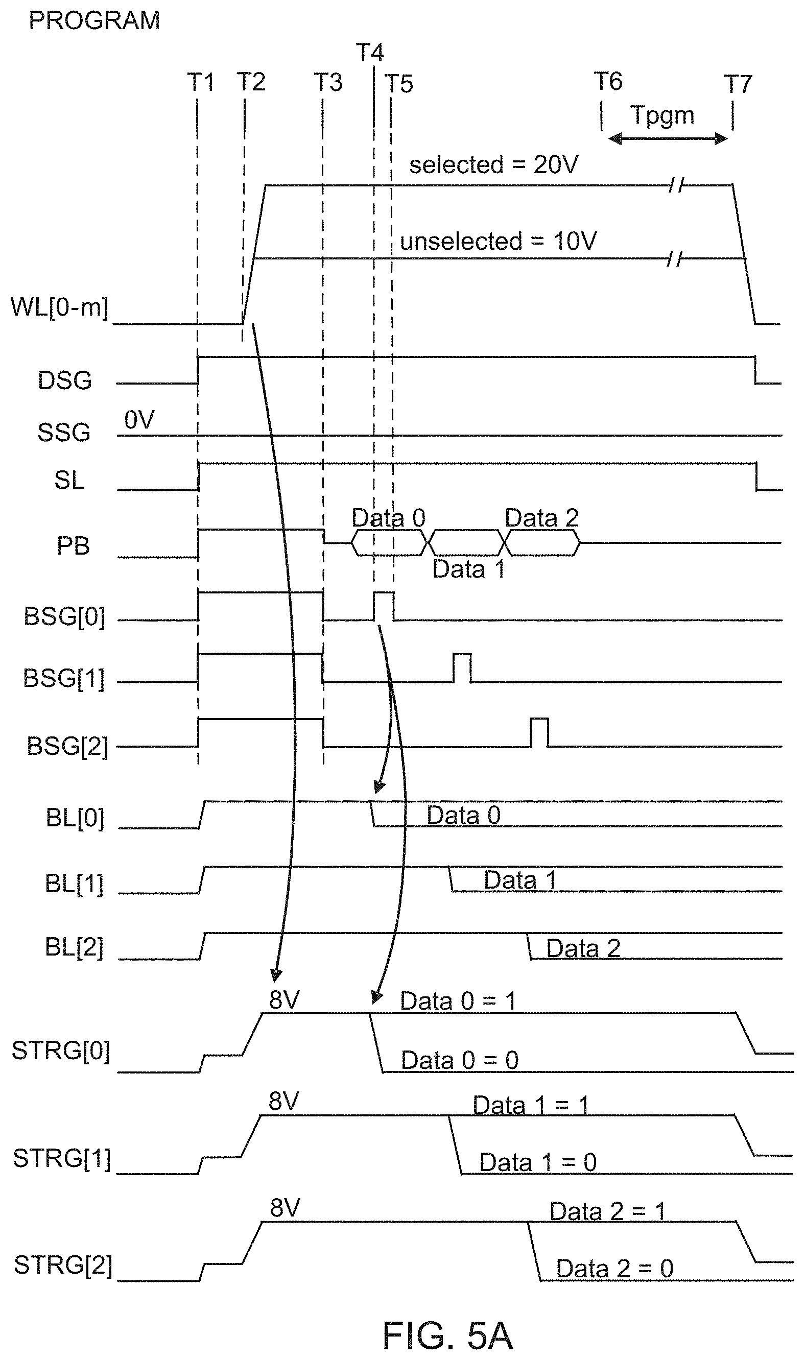
D00015
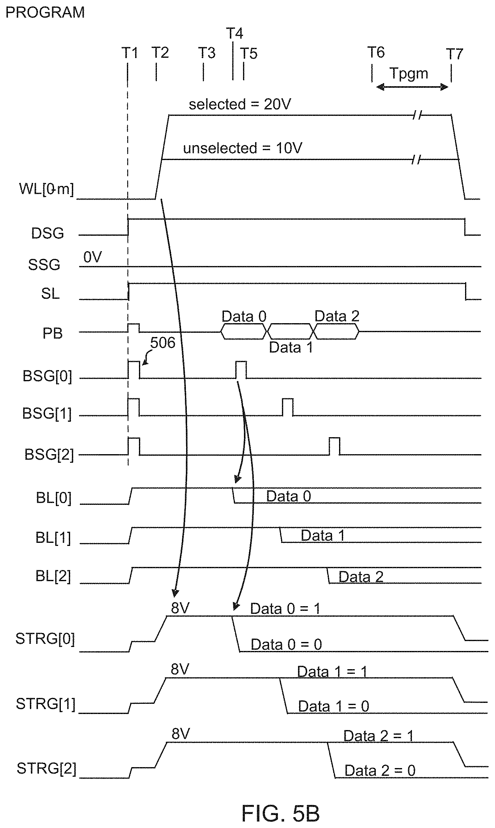
D00016
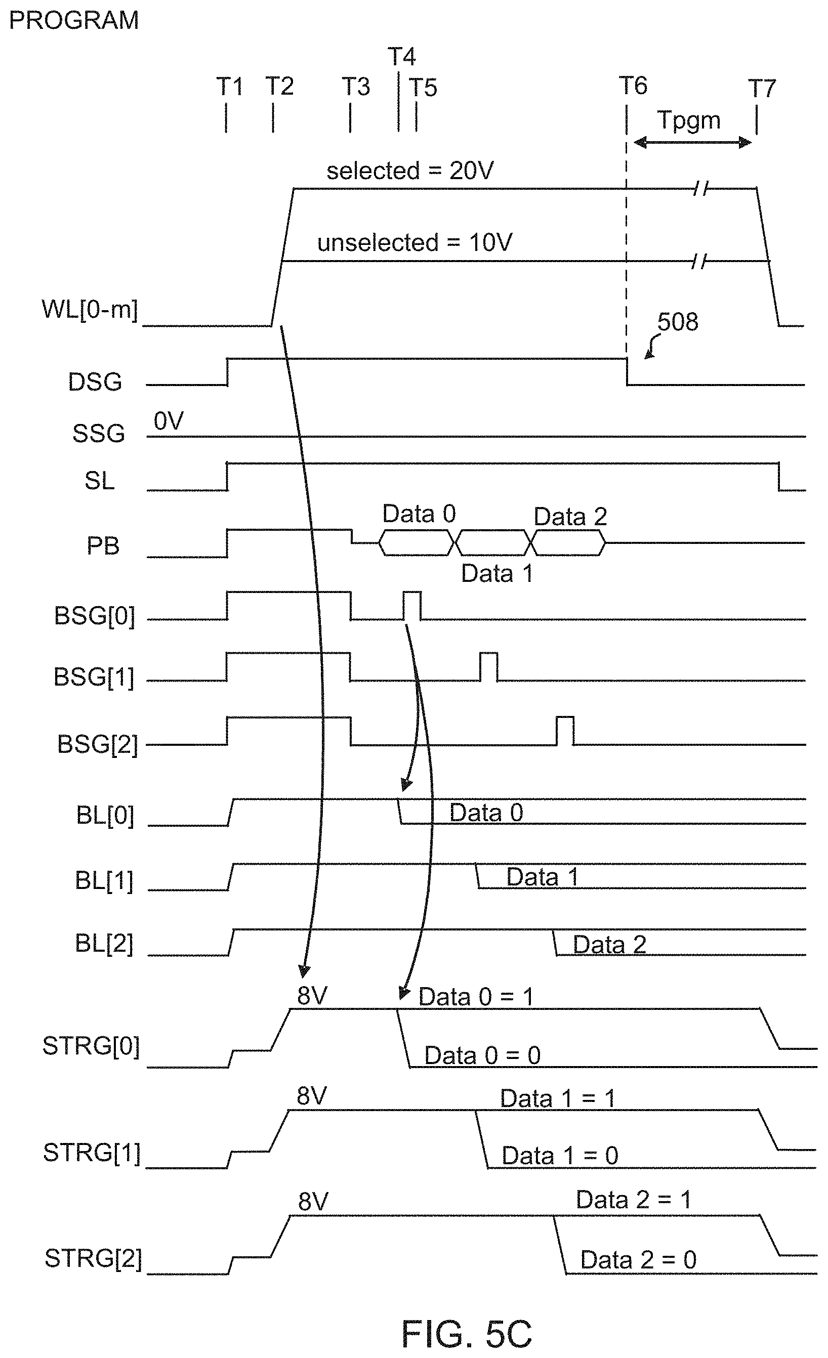
D00017

D00018
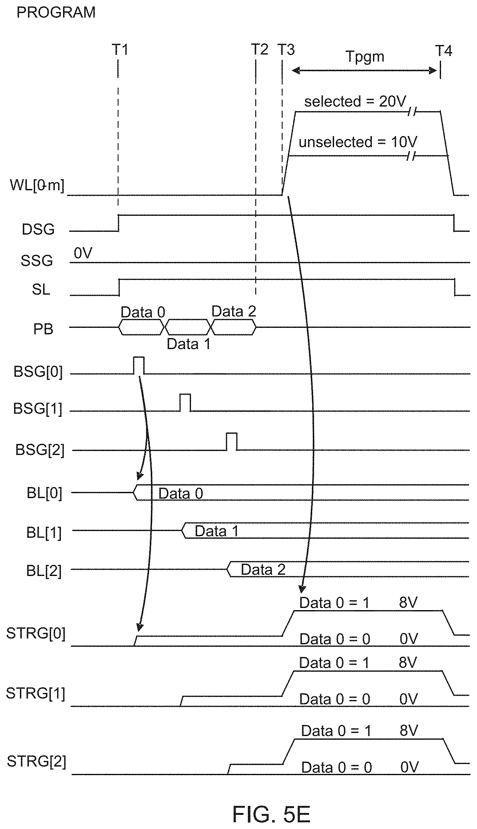
D00019
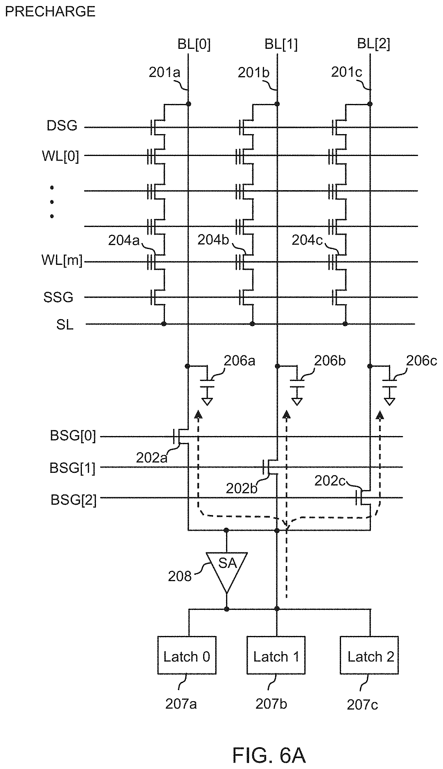
D00020
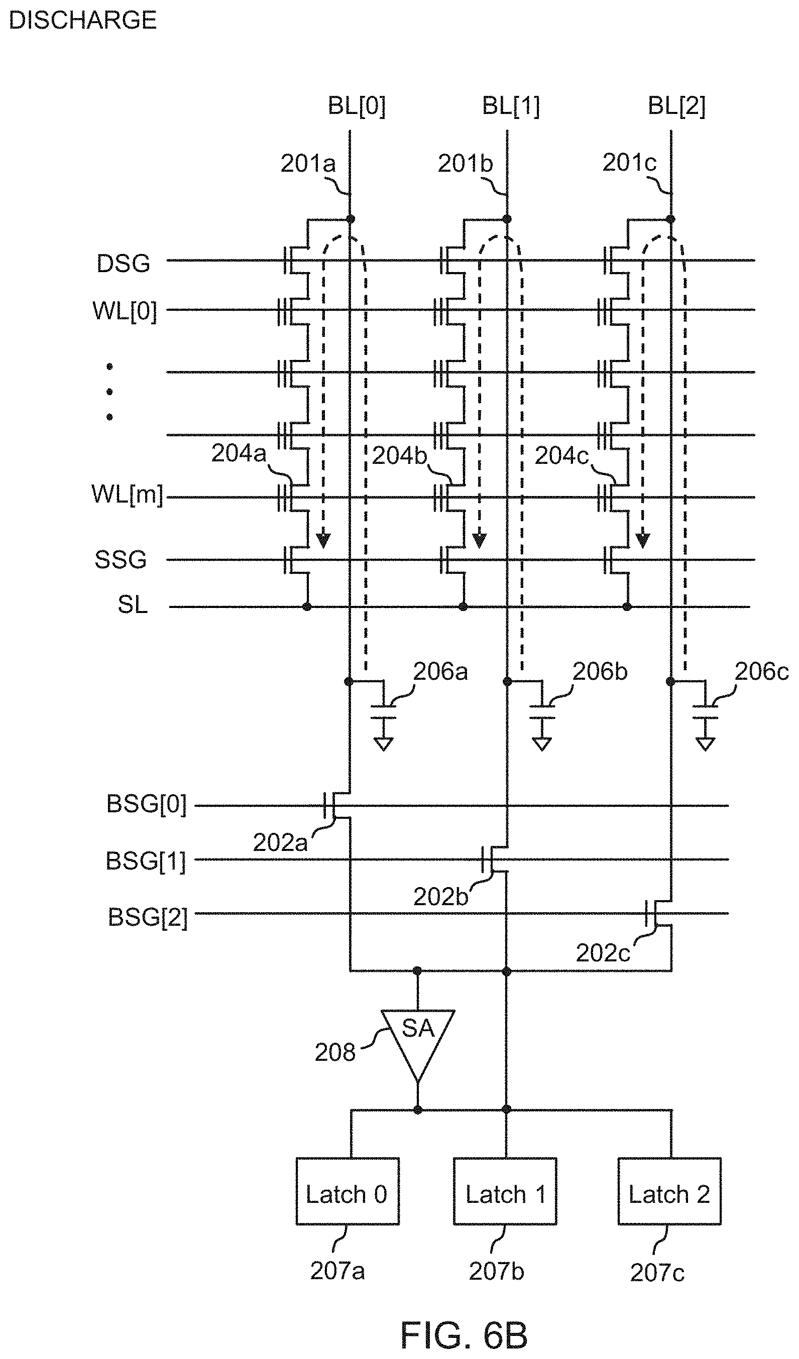
D00021
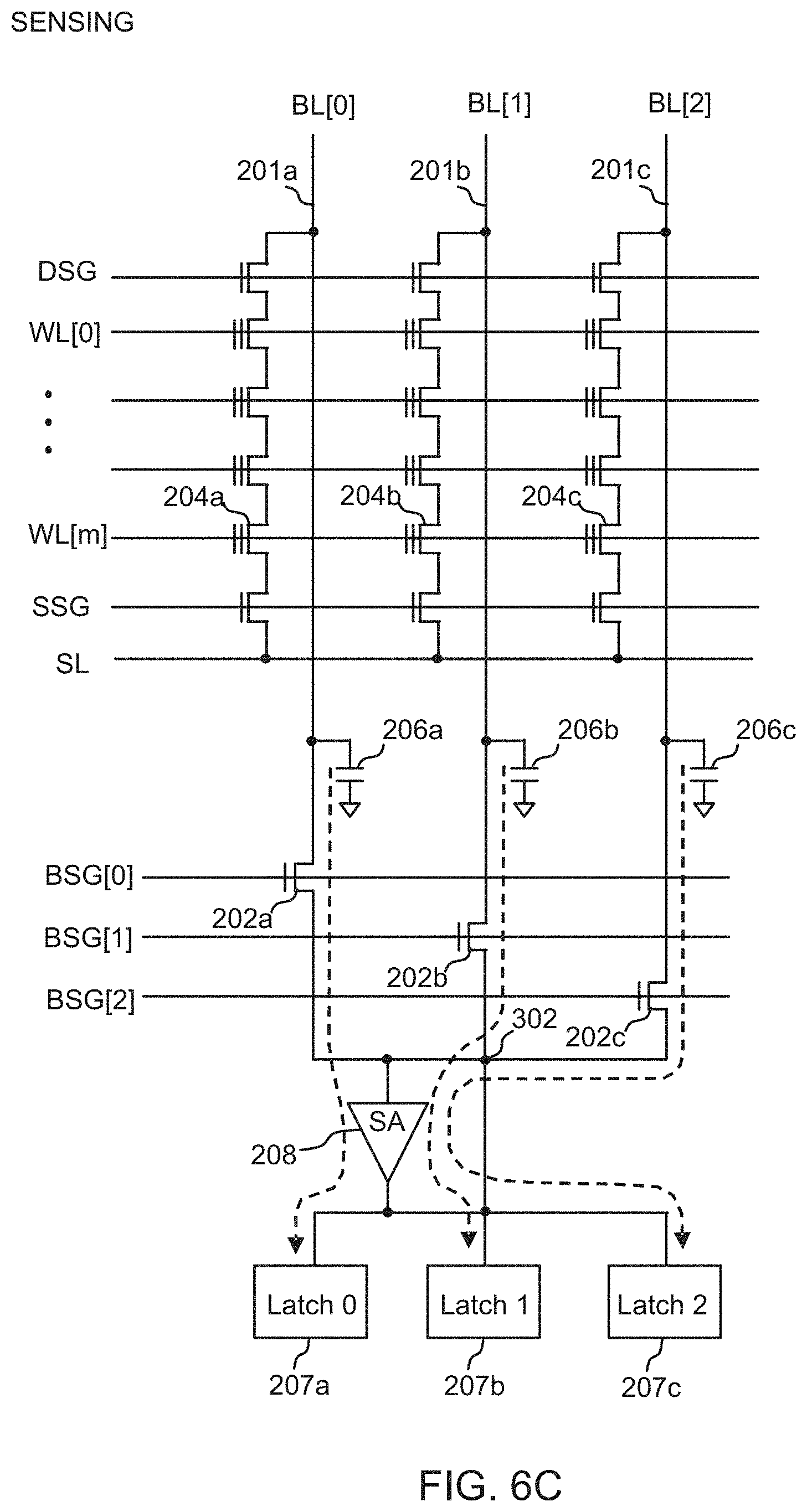
D00022
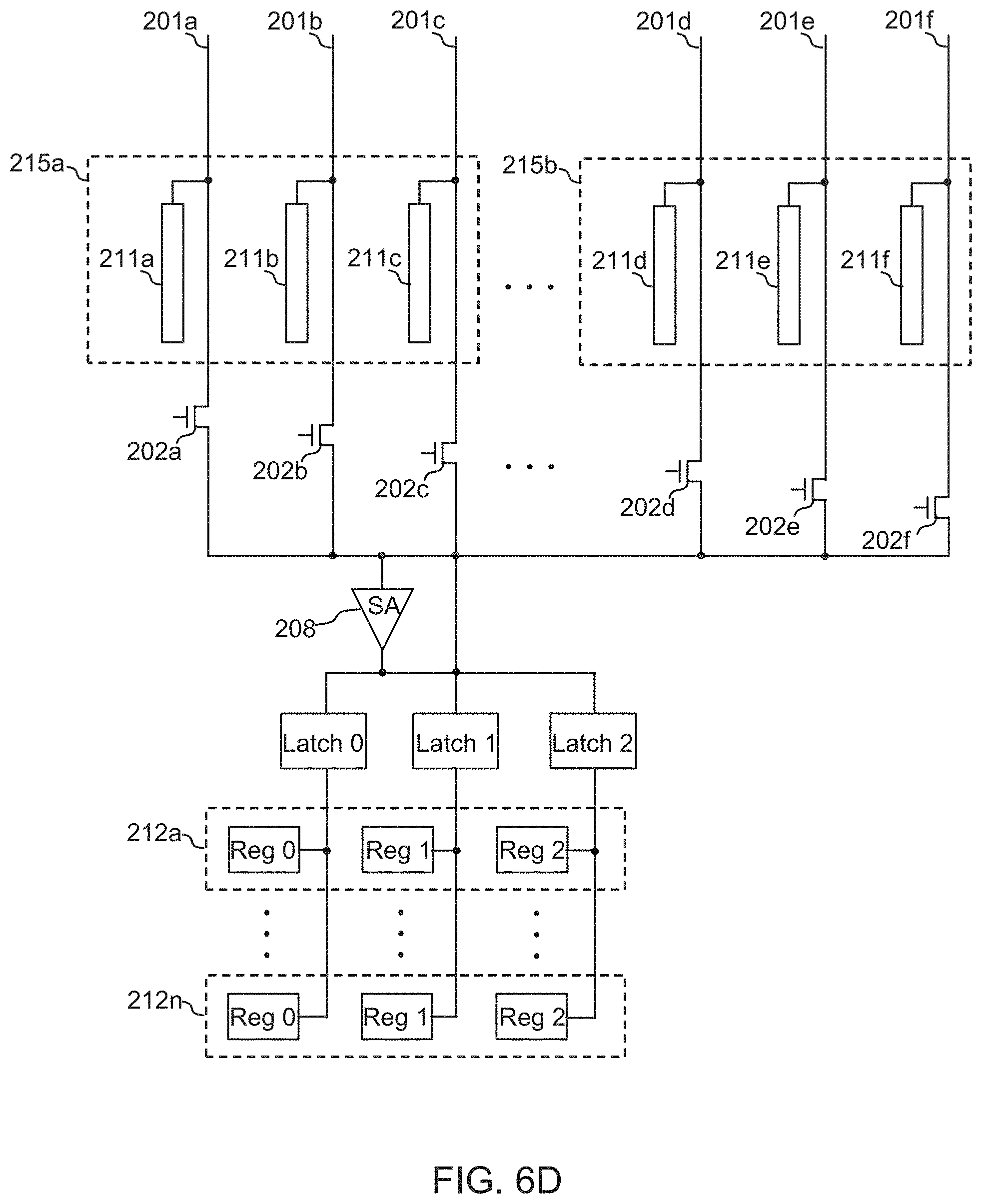
D00023

D00024
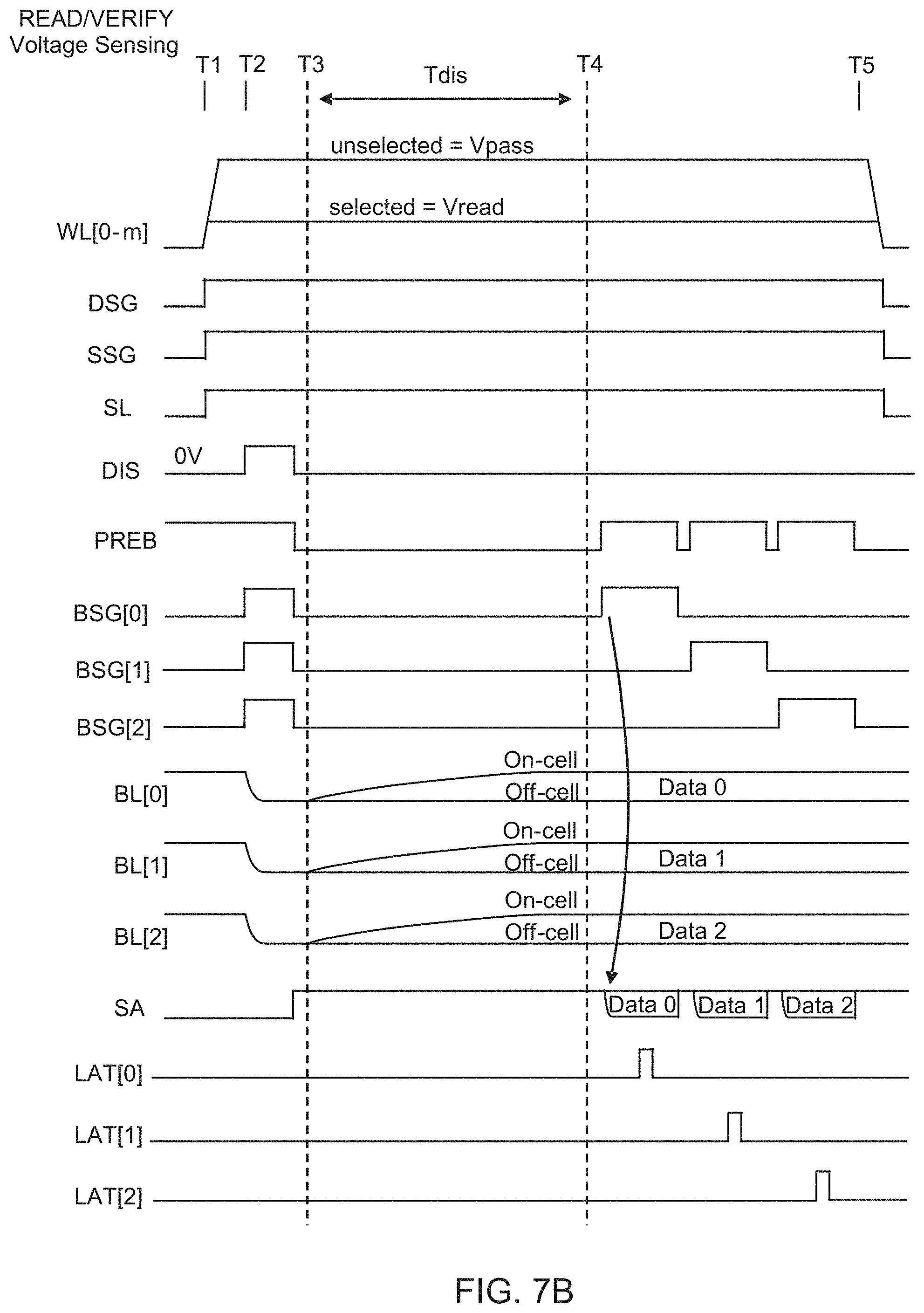
D00025
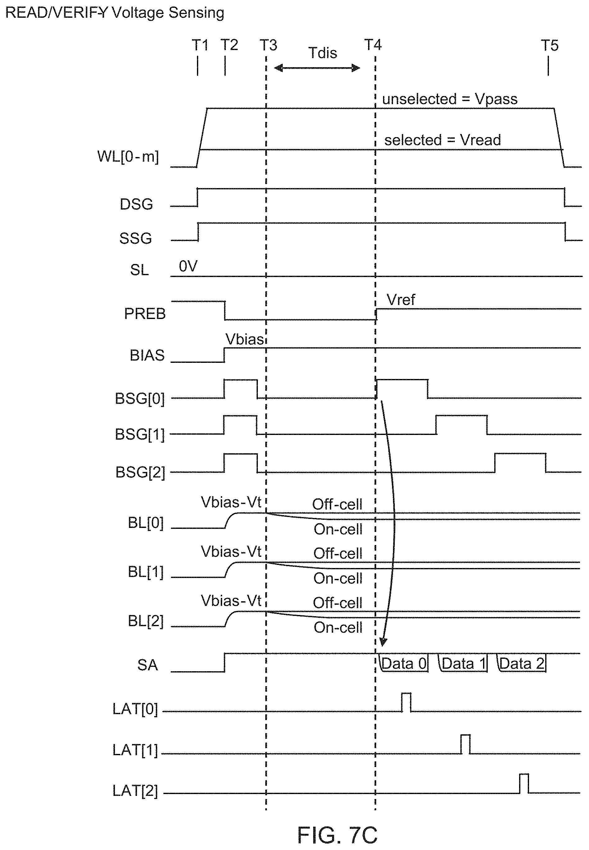
D00026
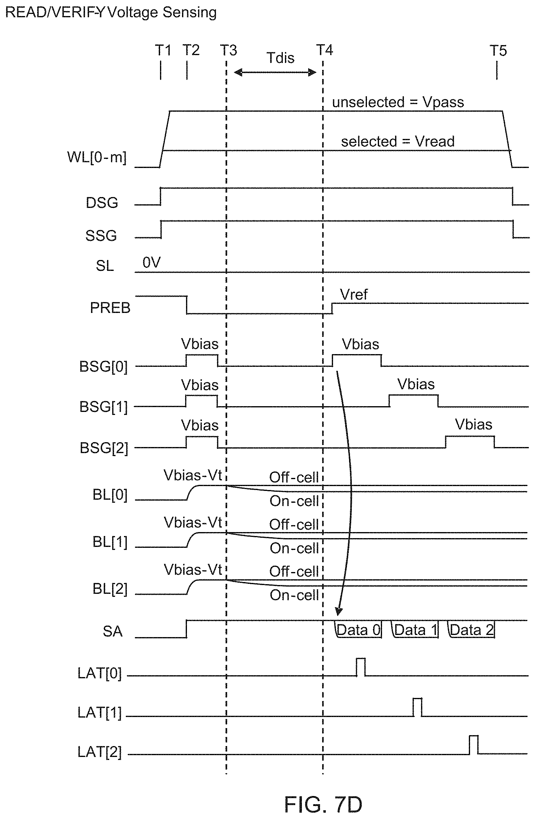
D00027
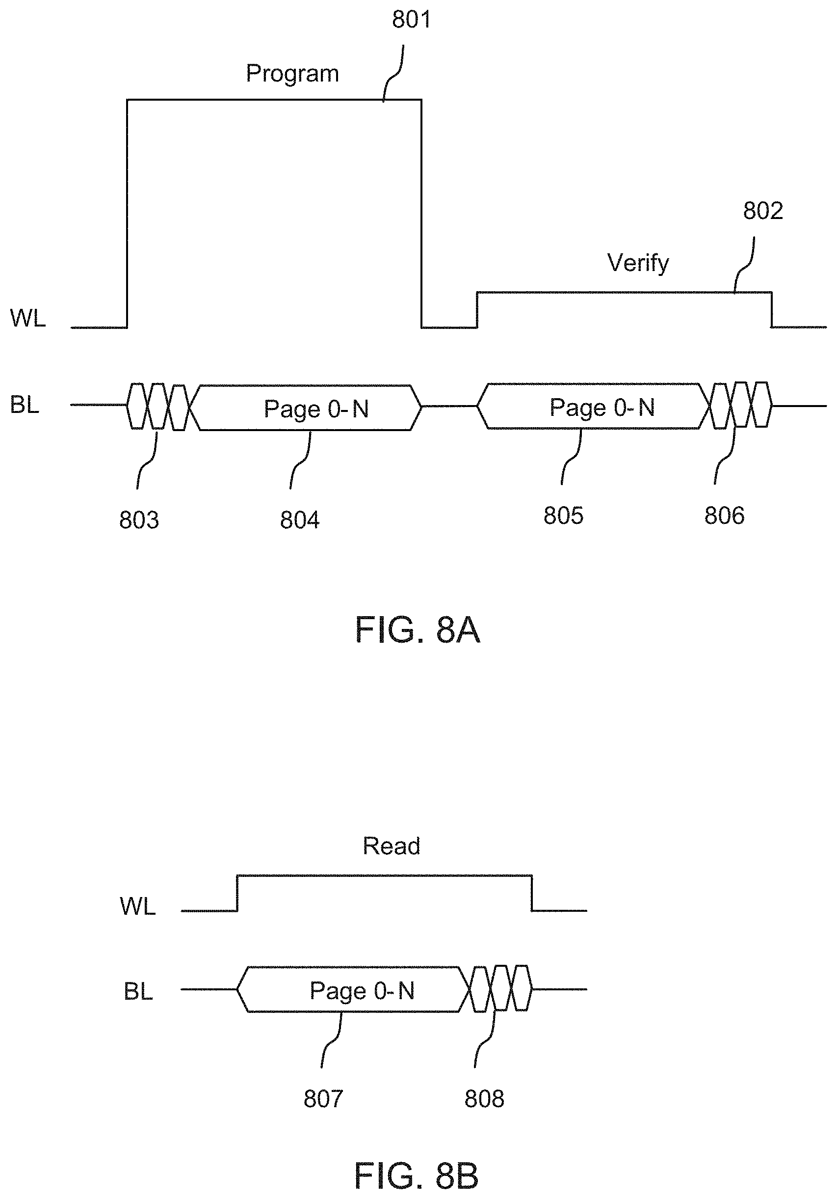
D00028
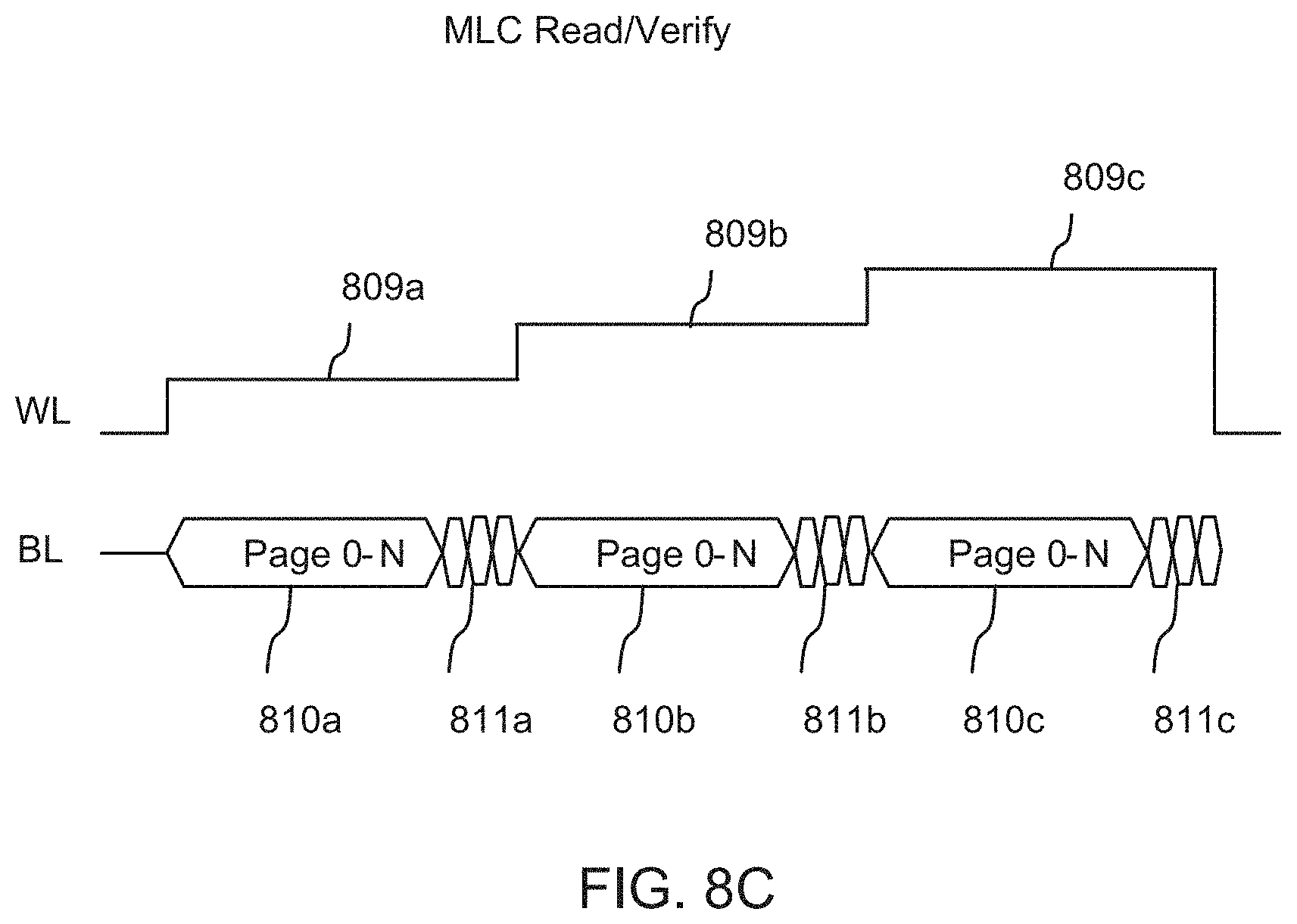
D00029
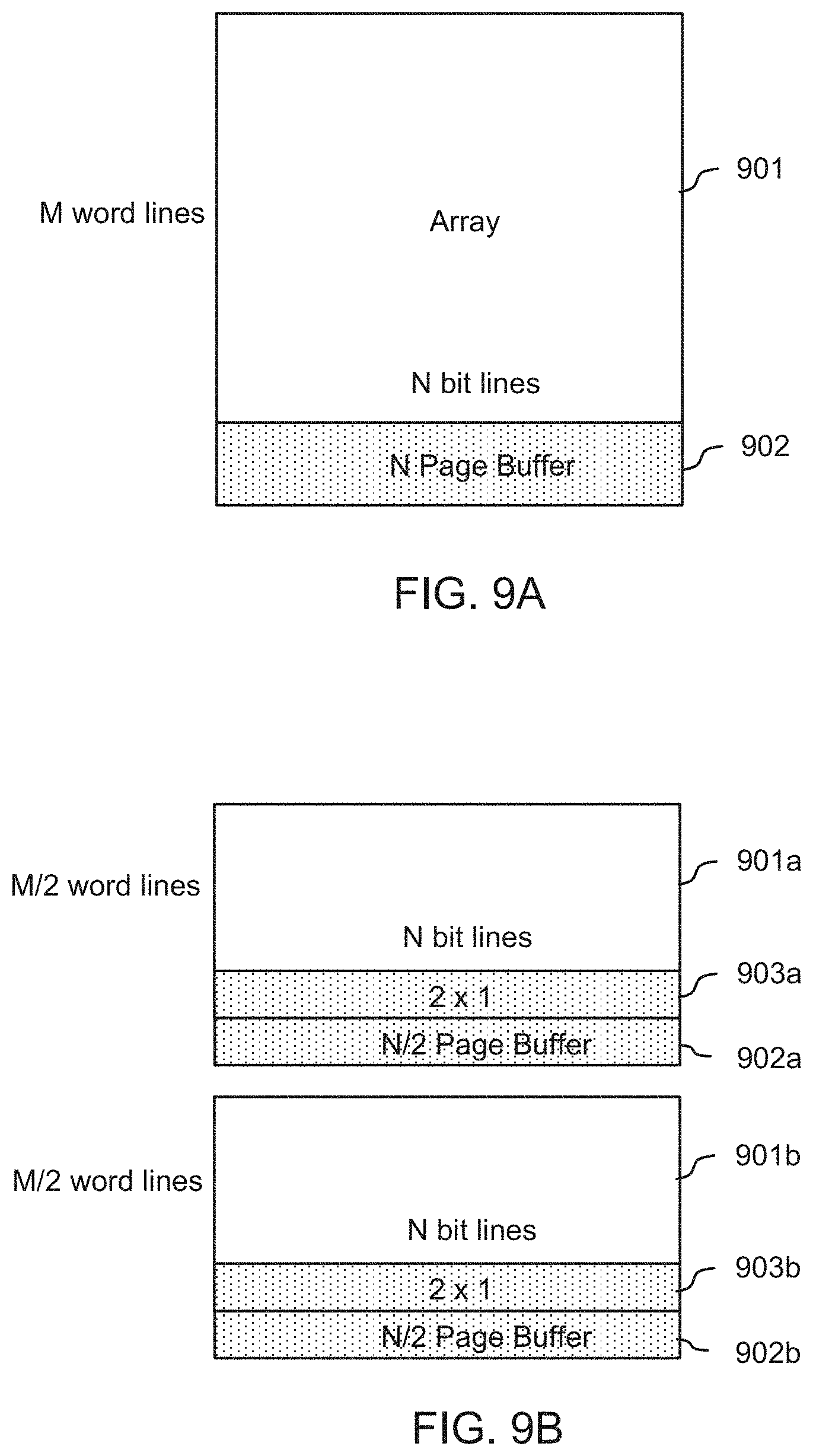
D00030
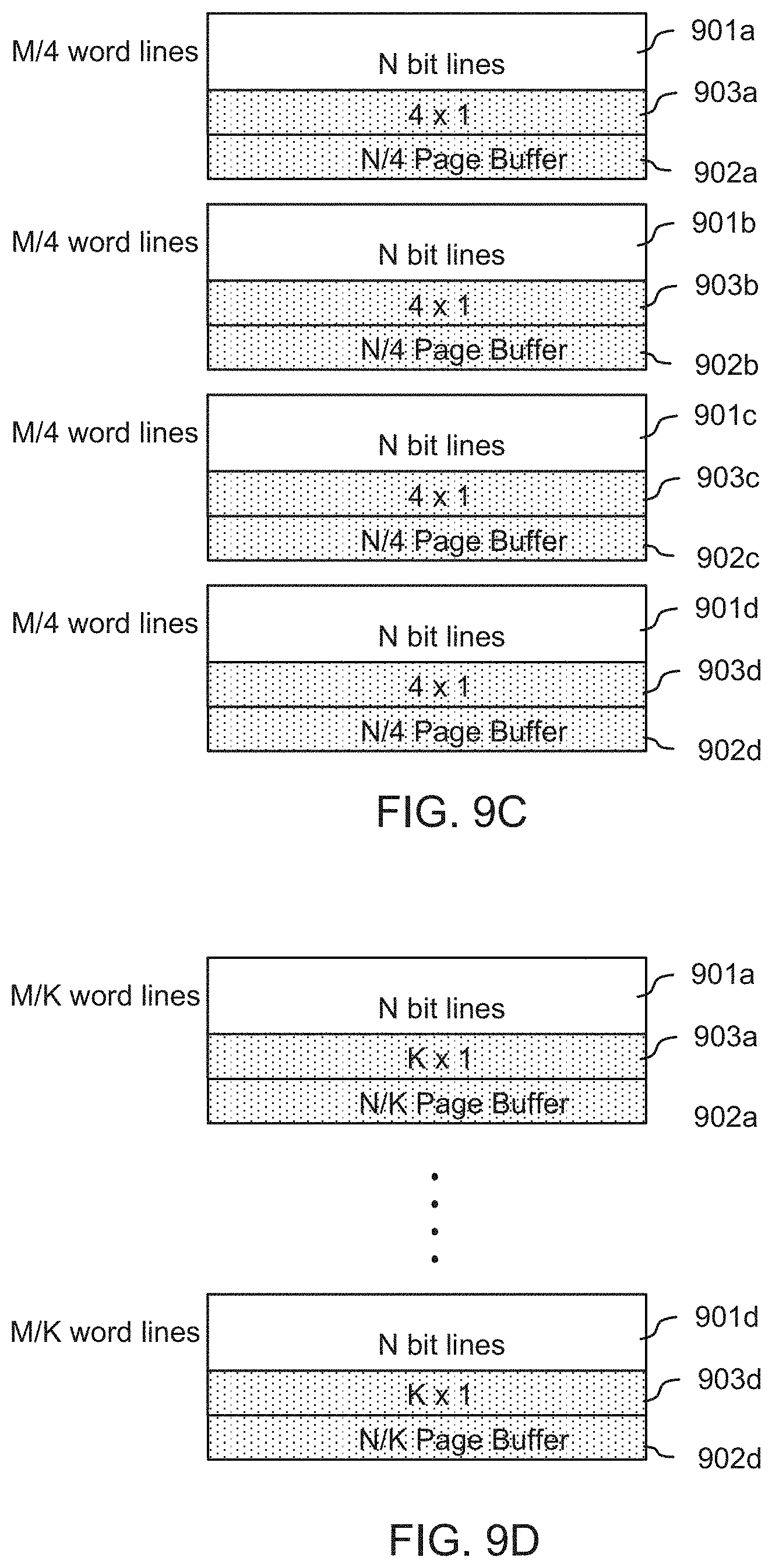
D00031
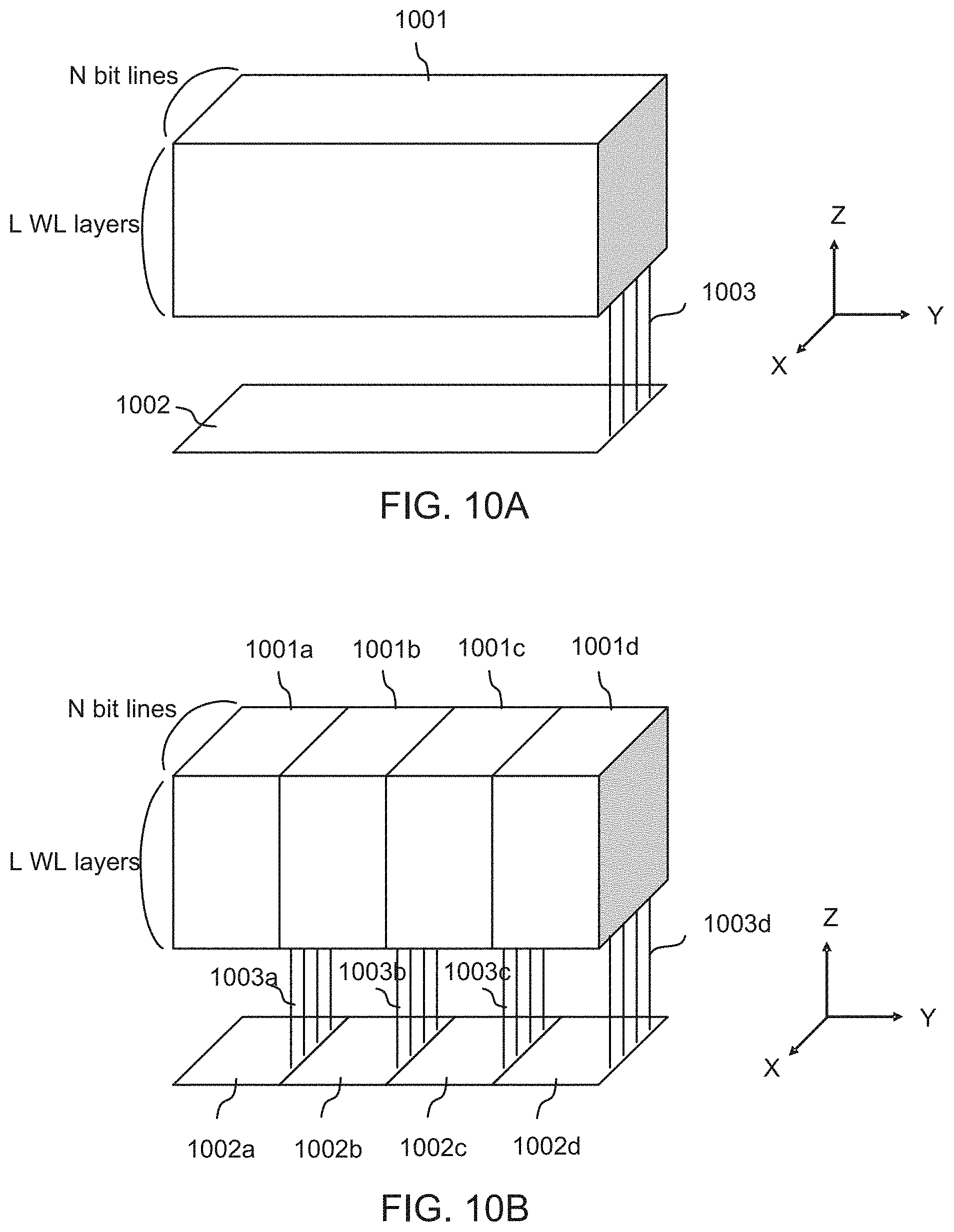
D00032
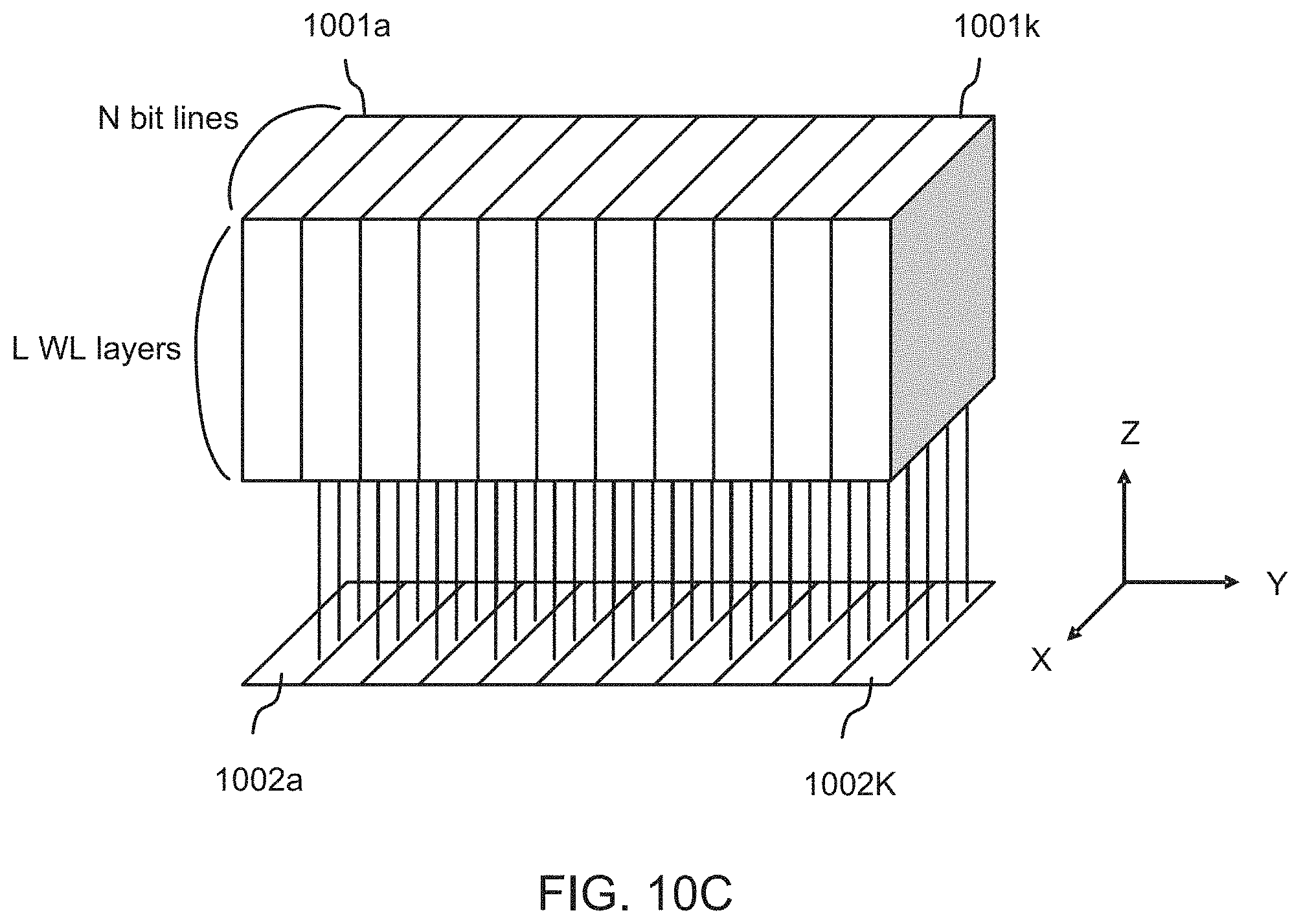
D00033
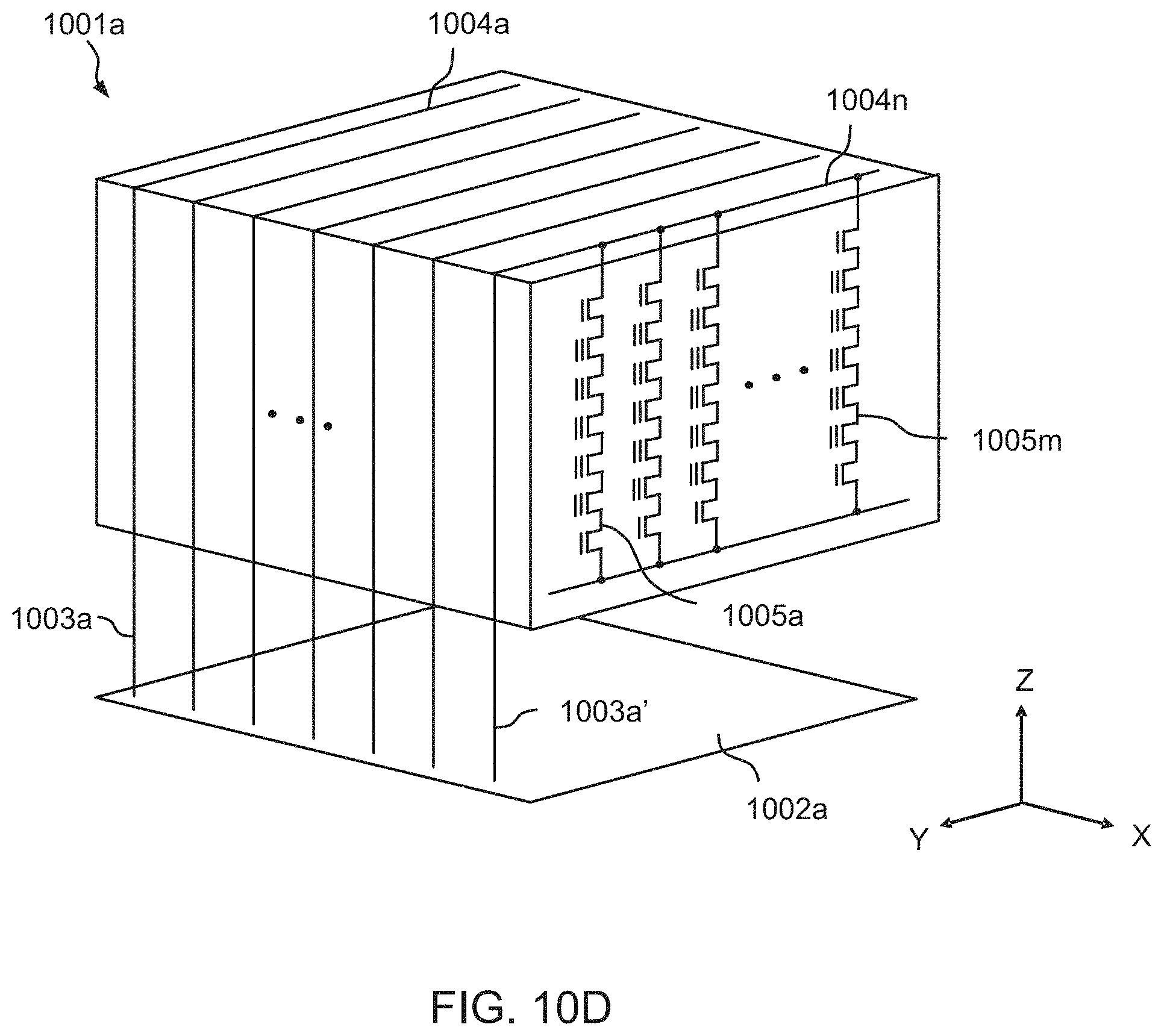
D00034
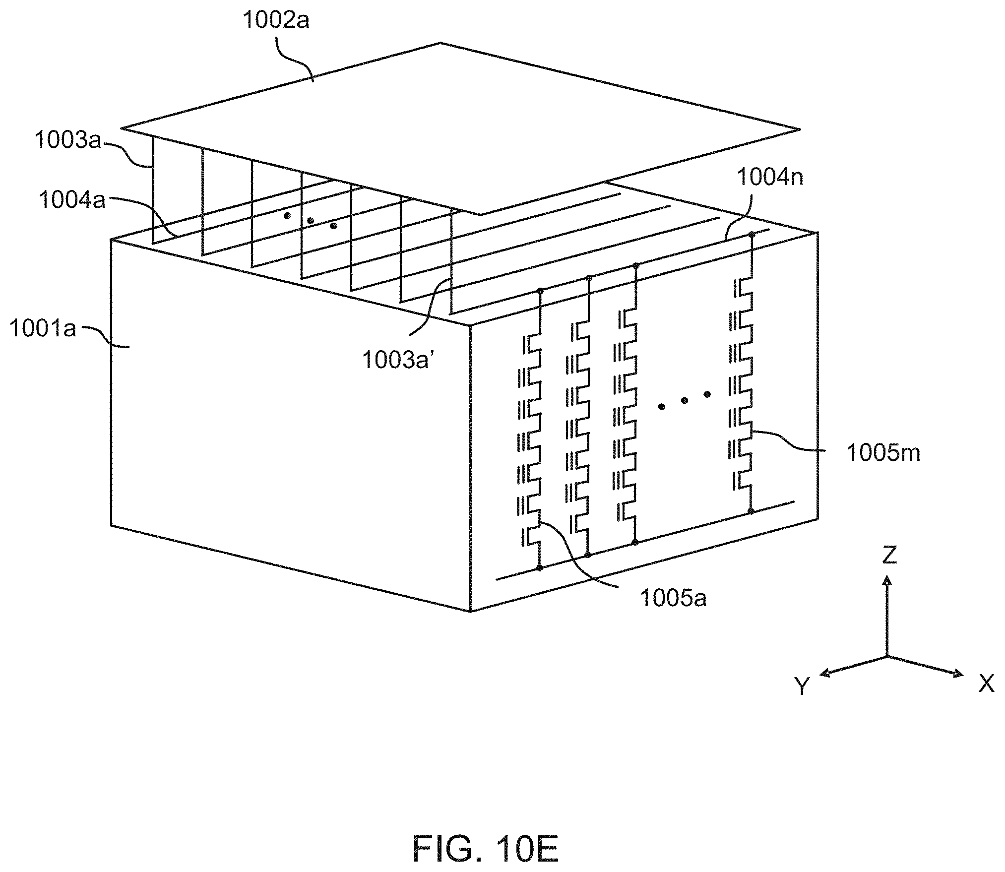
D00035
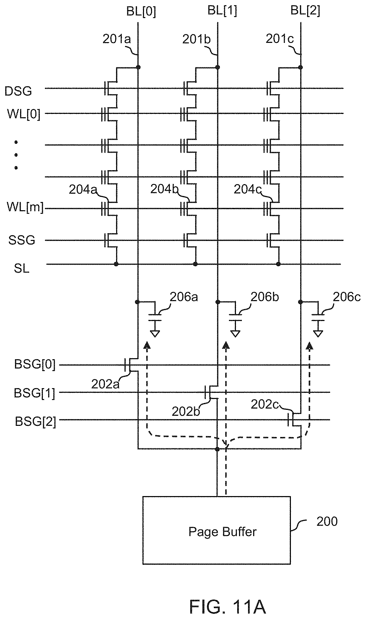
D00036
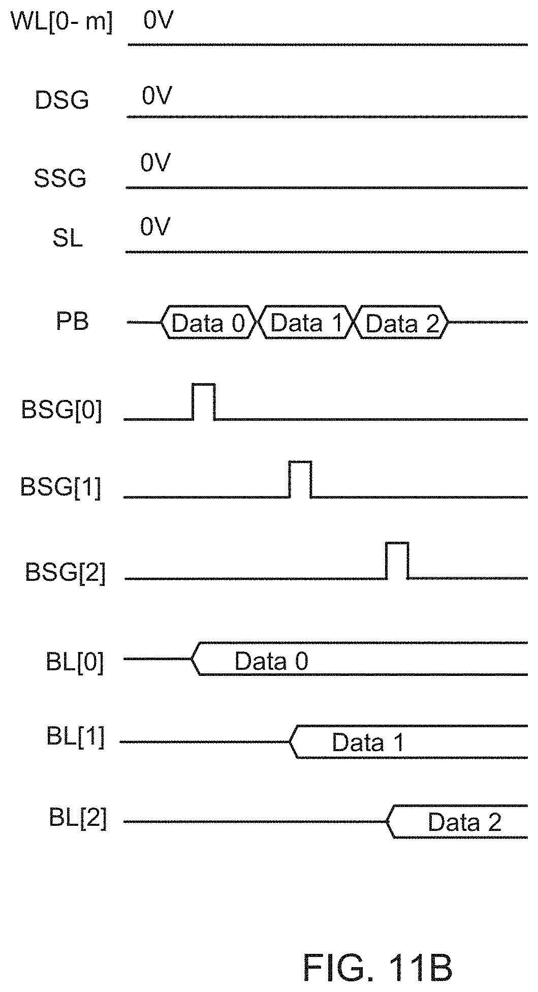
D00037

D00038
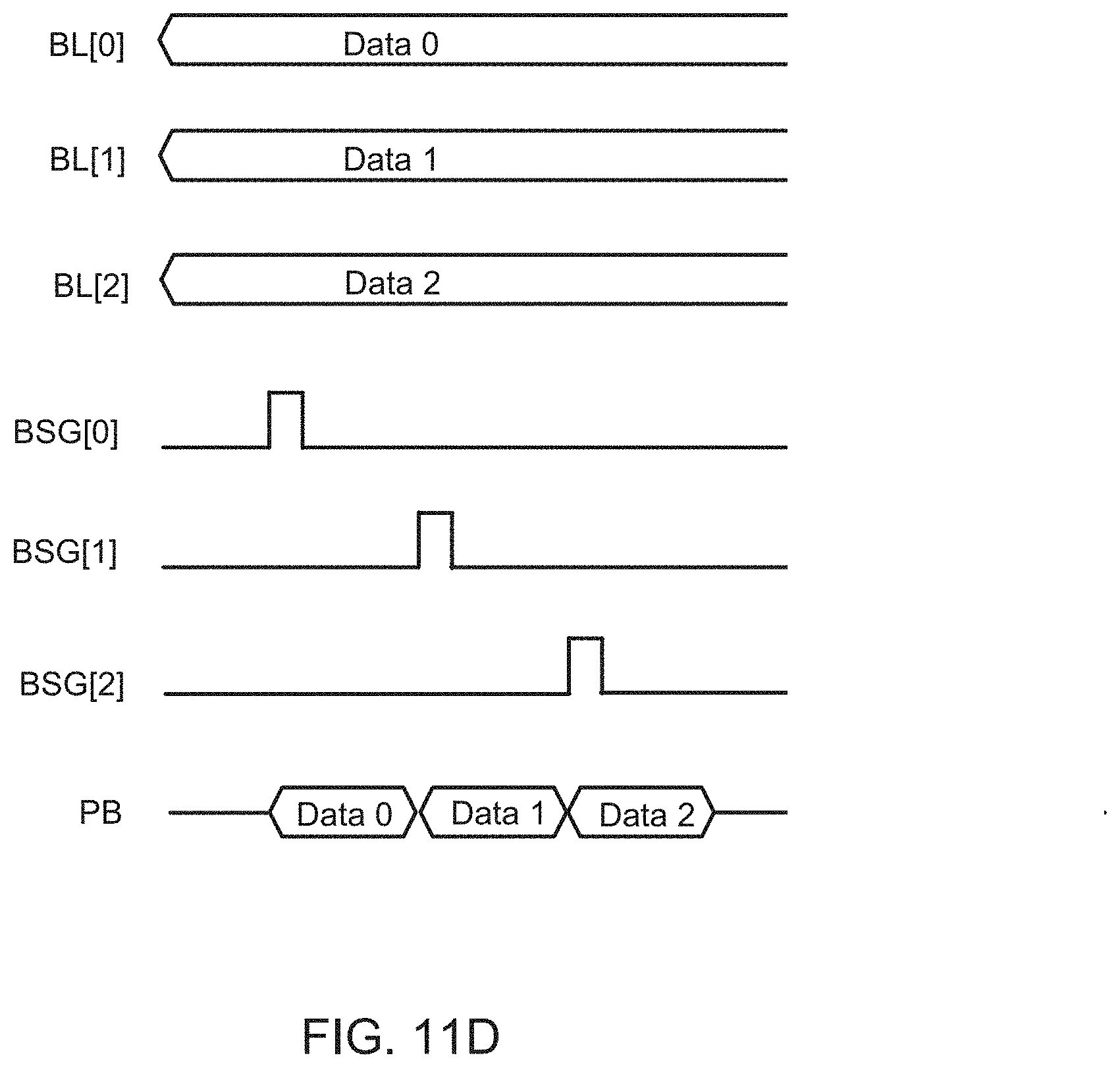
D00039
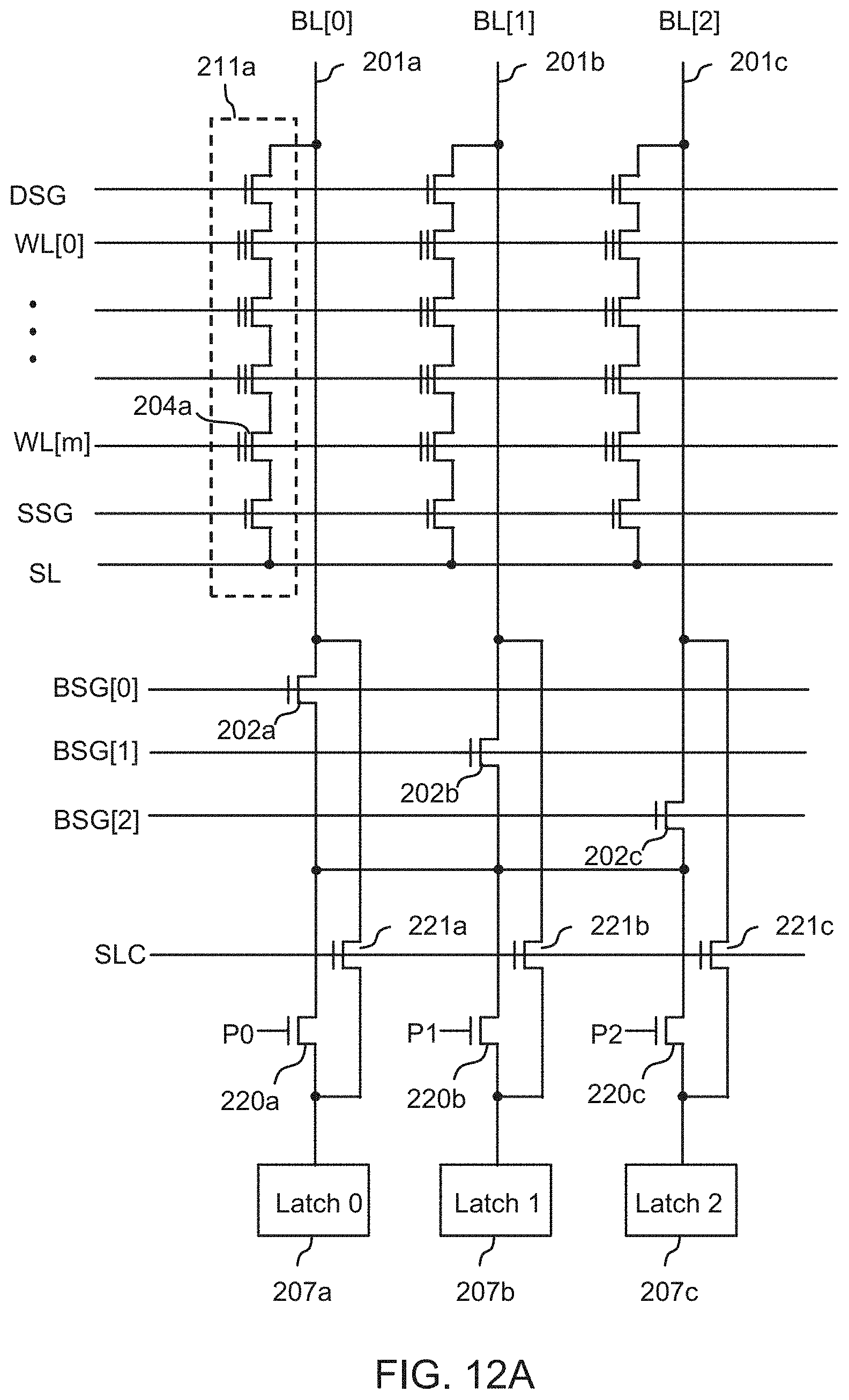
D00040
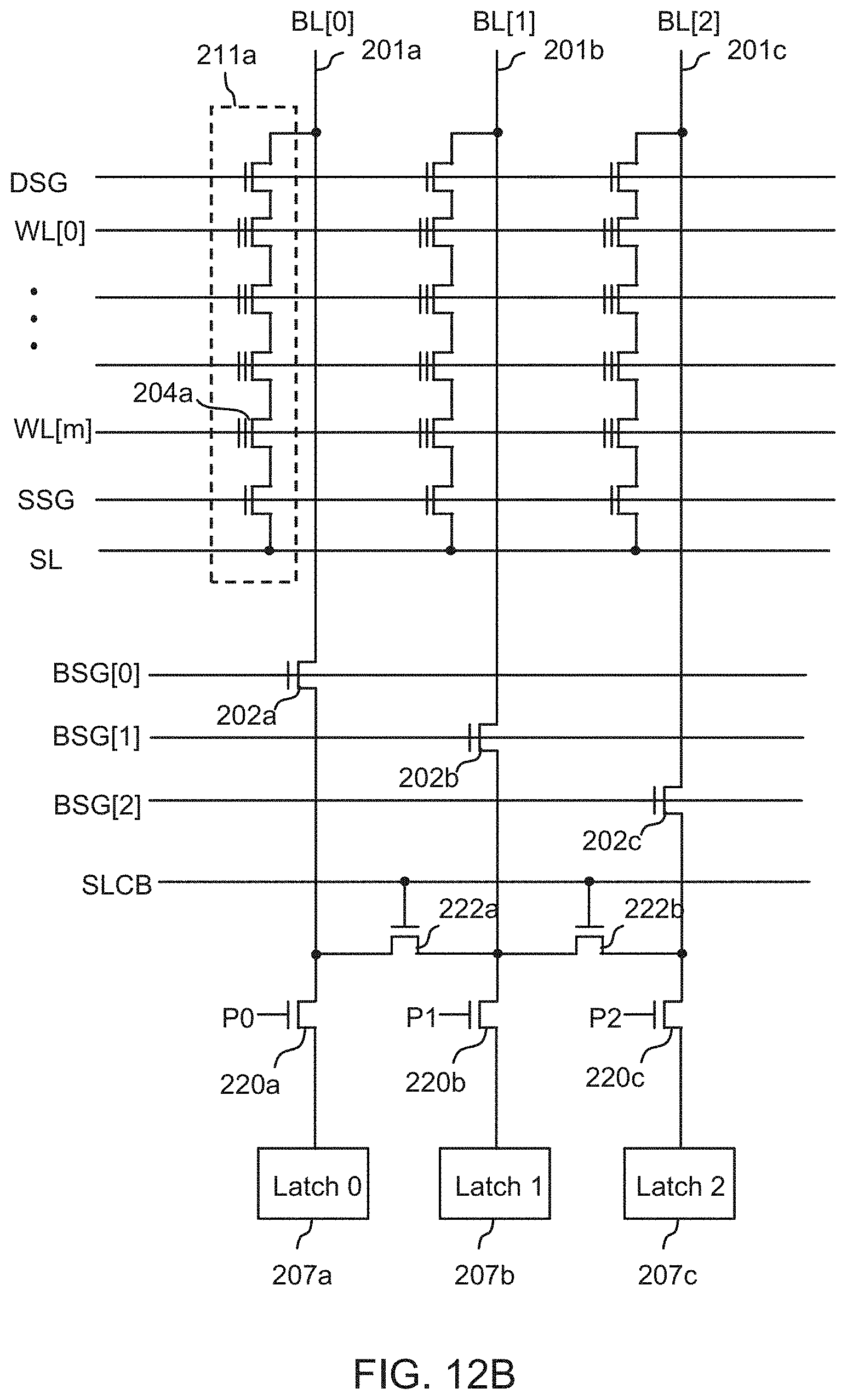
D00041
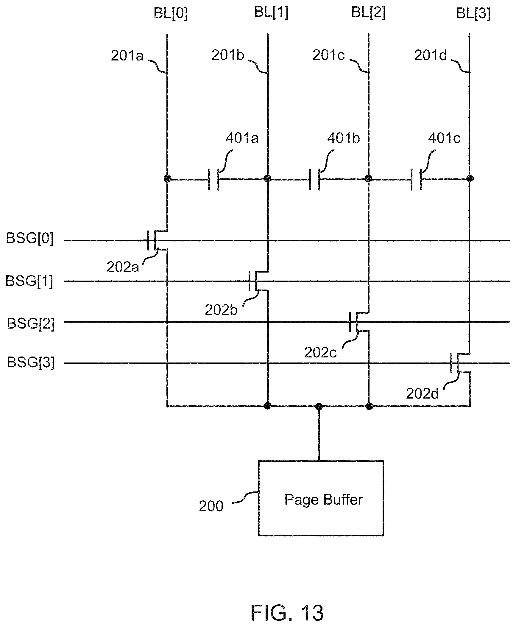
D00042
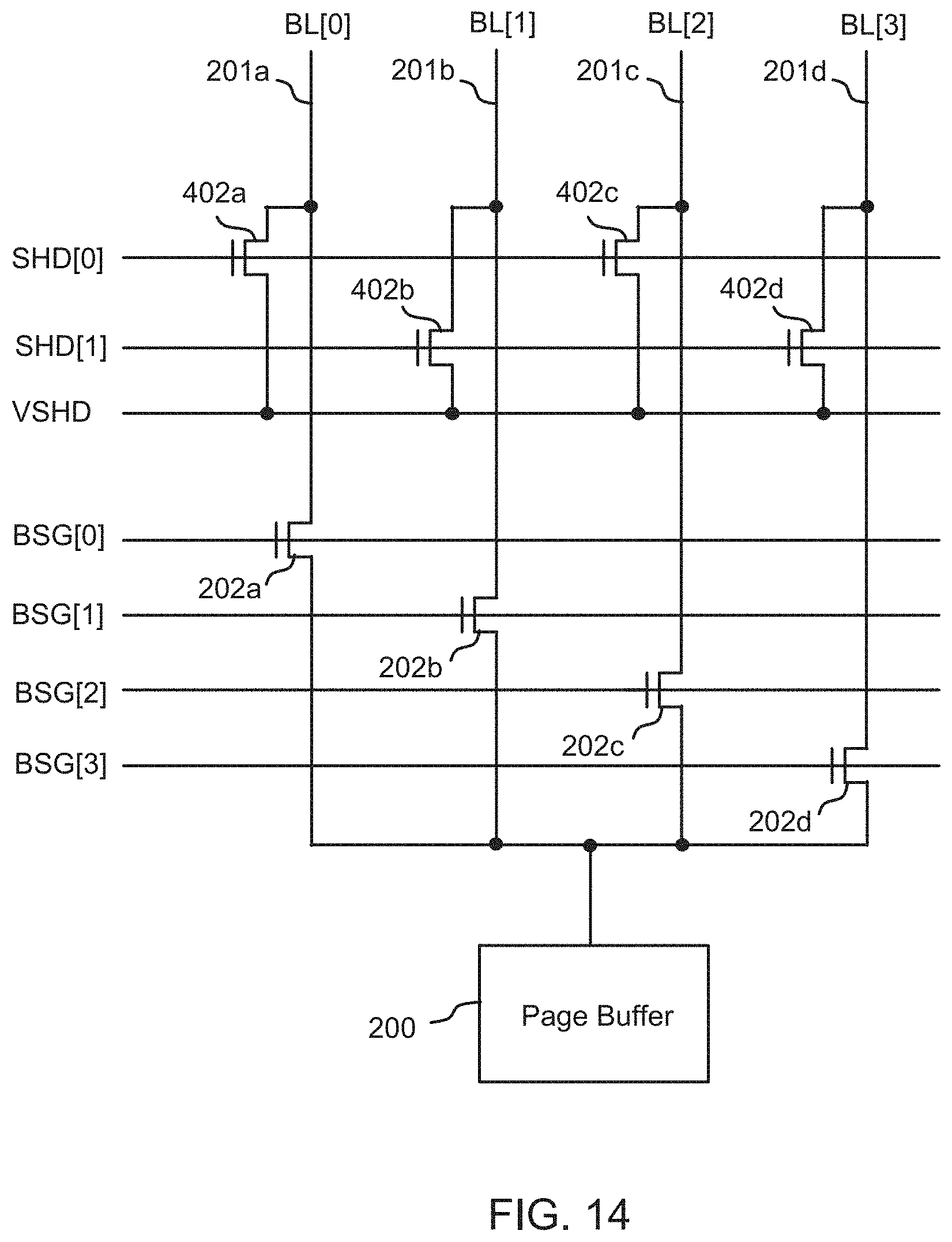
D00043
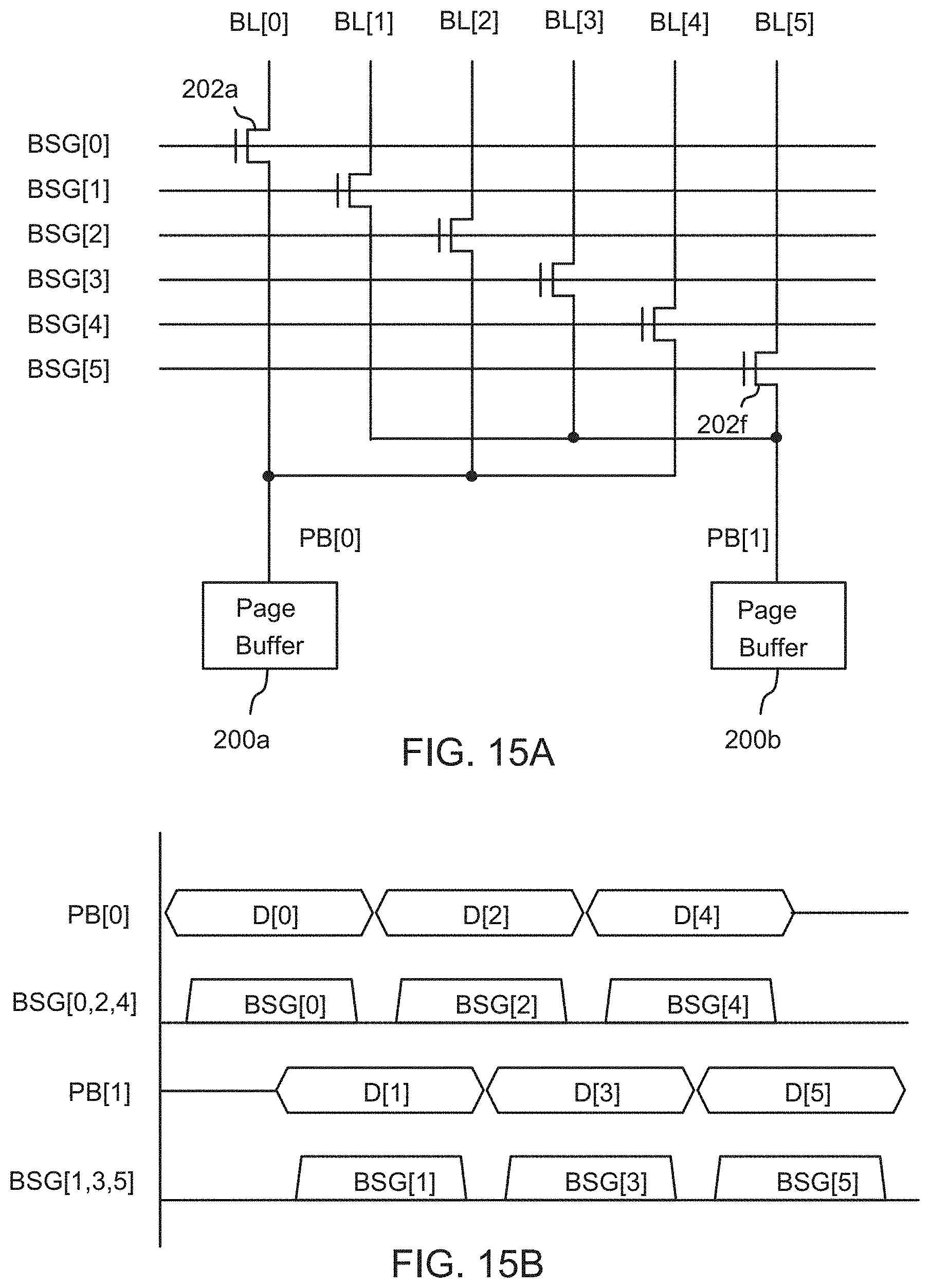
D00044
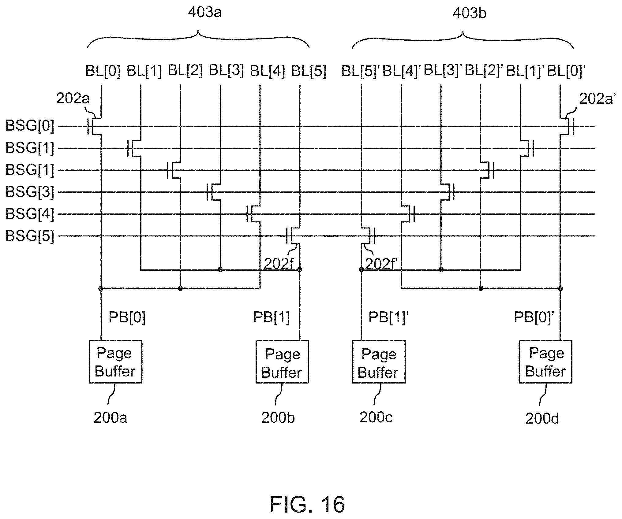
D00045

D00046
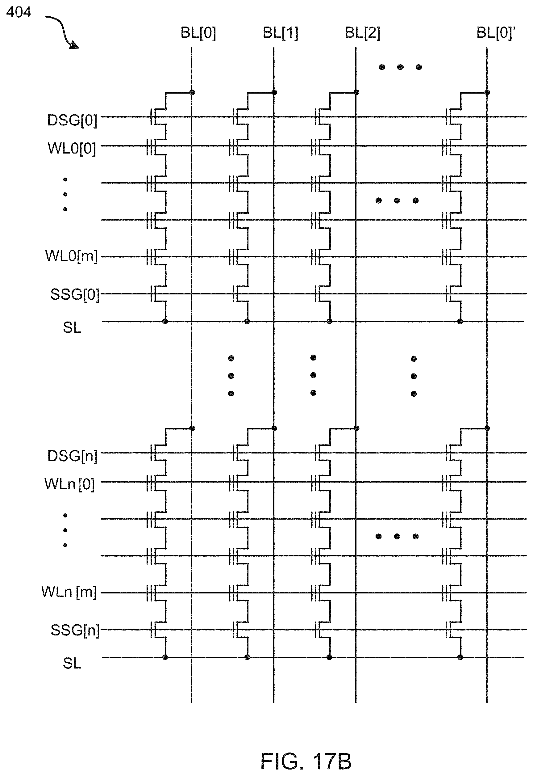
D00047
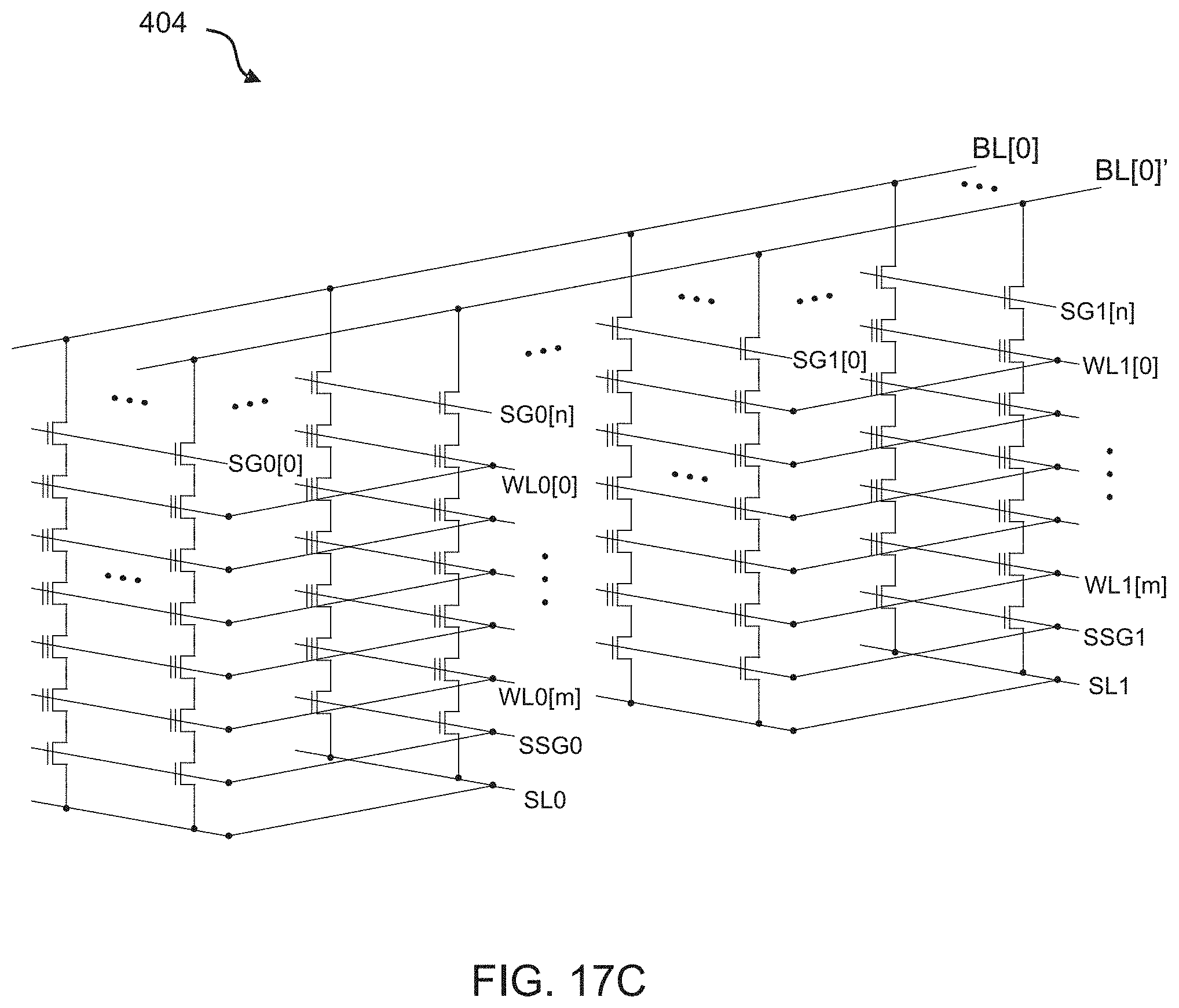
D00048
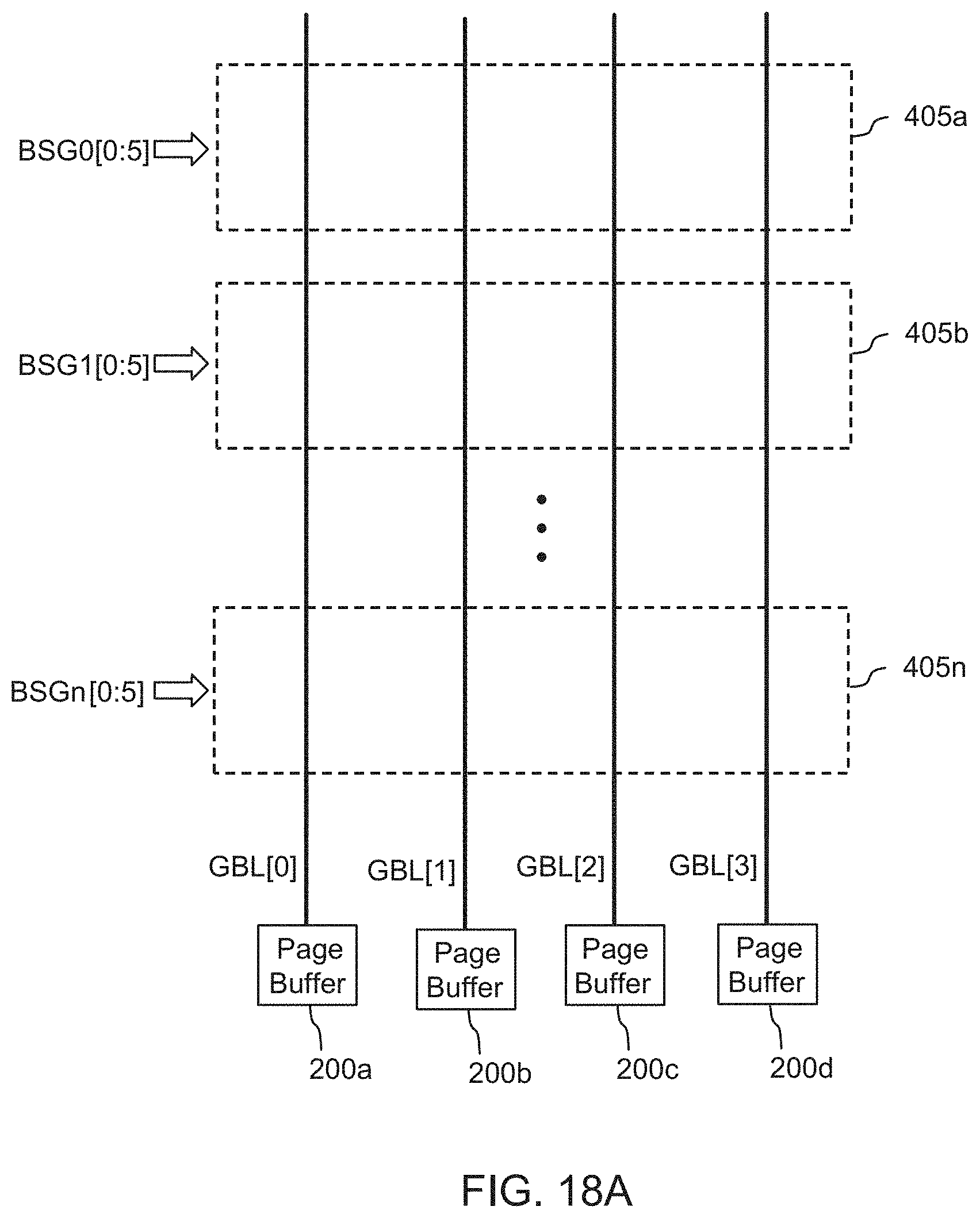
D00049
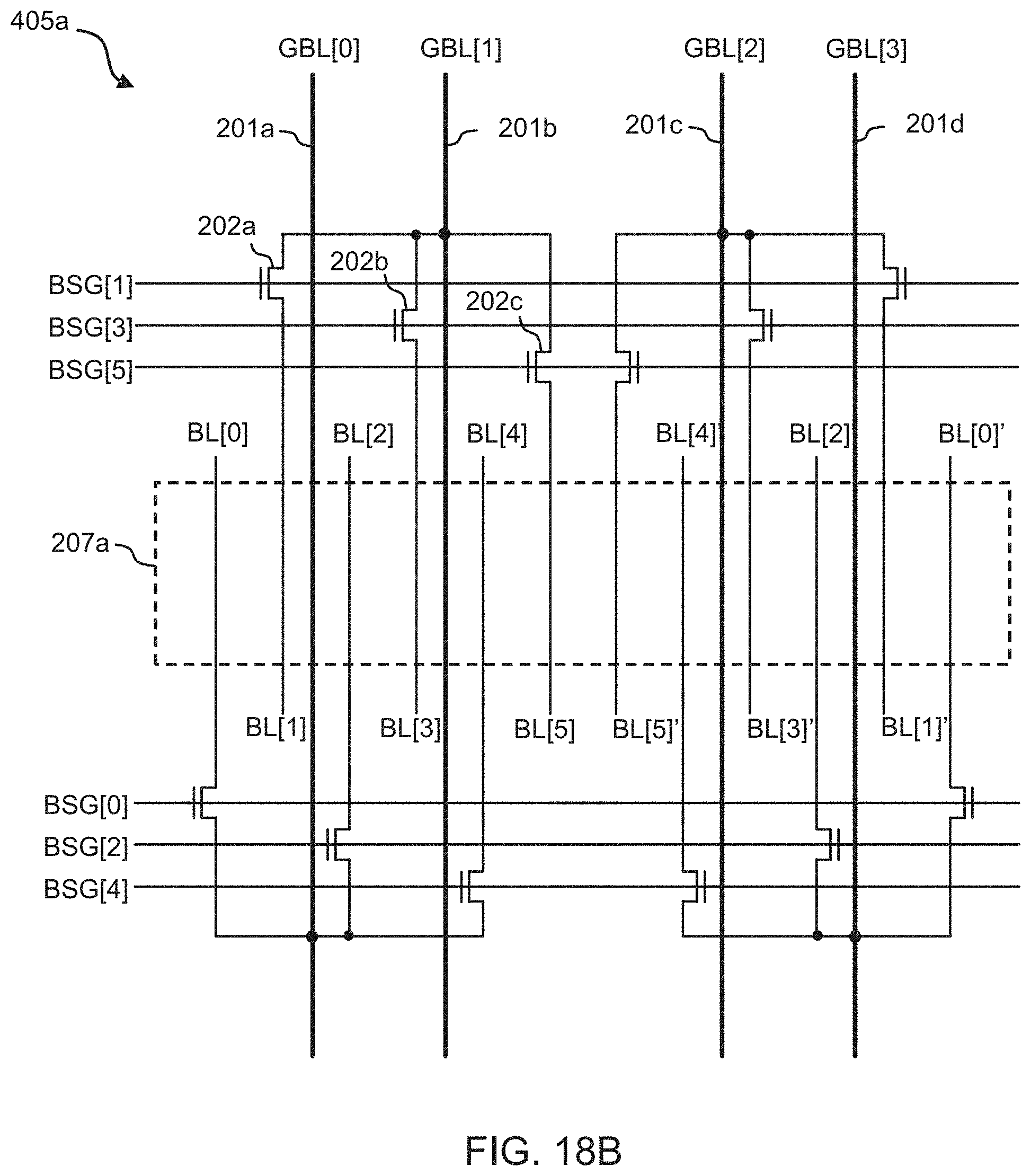
D00050
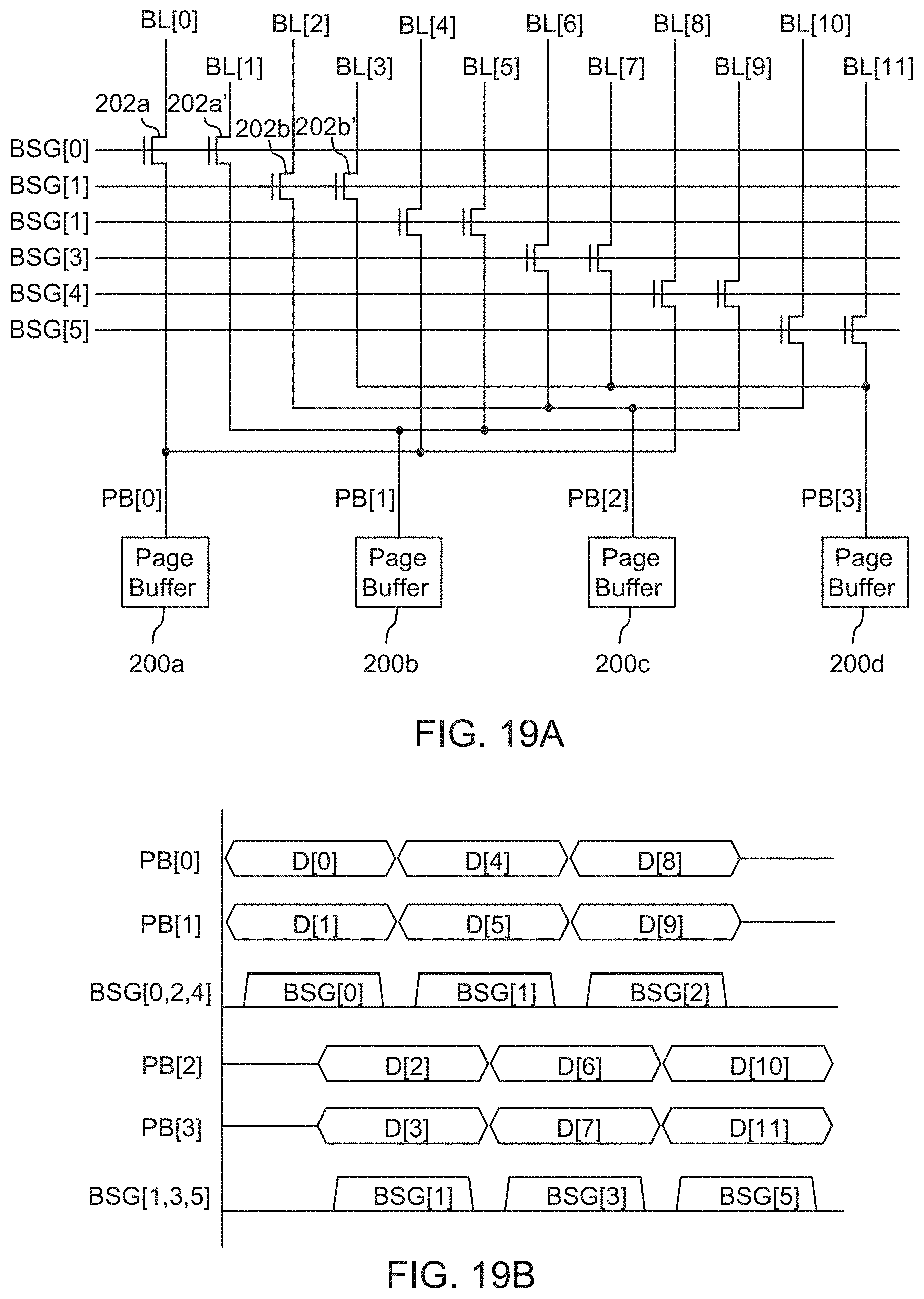
D00051
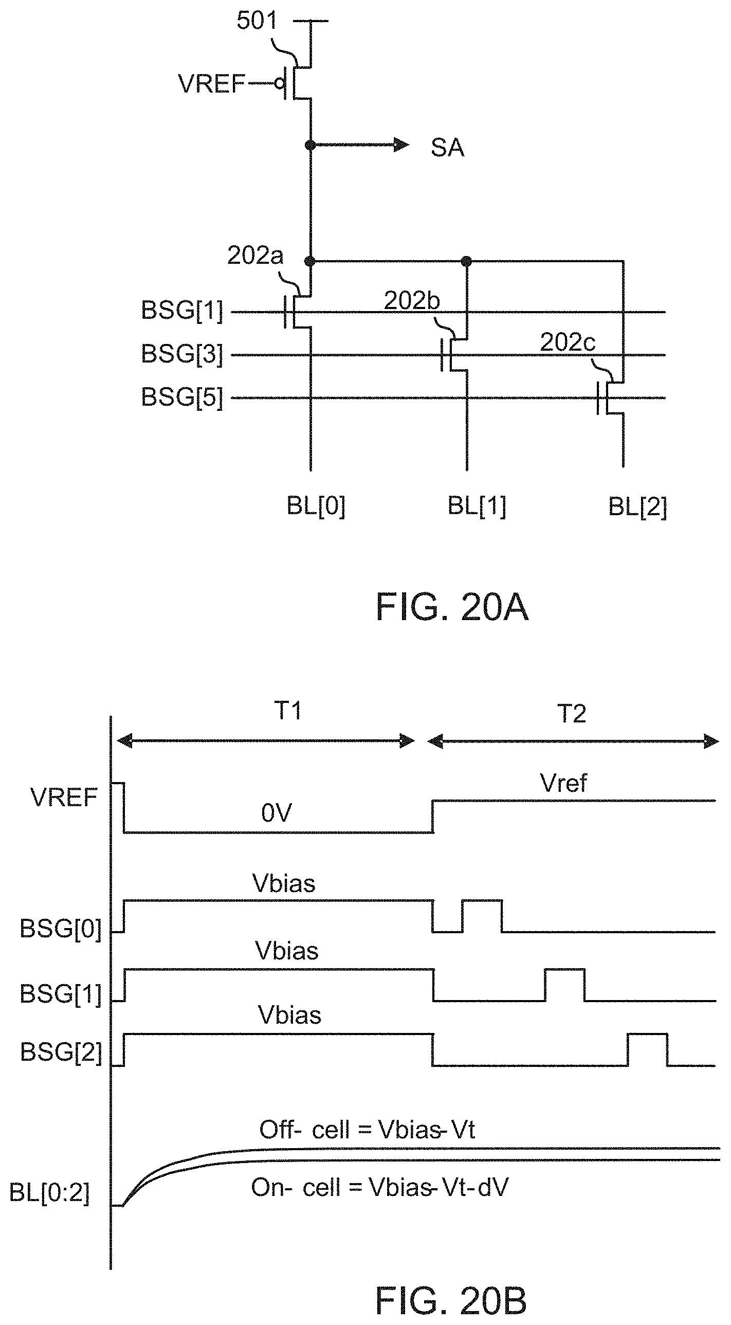
D00052
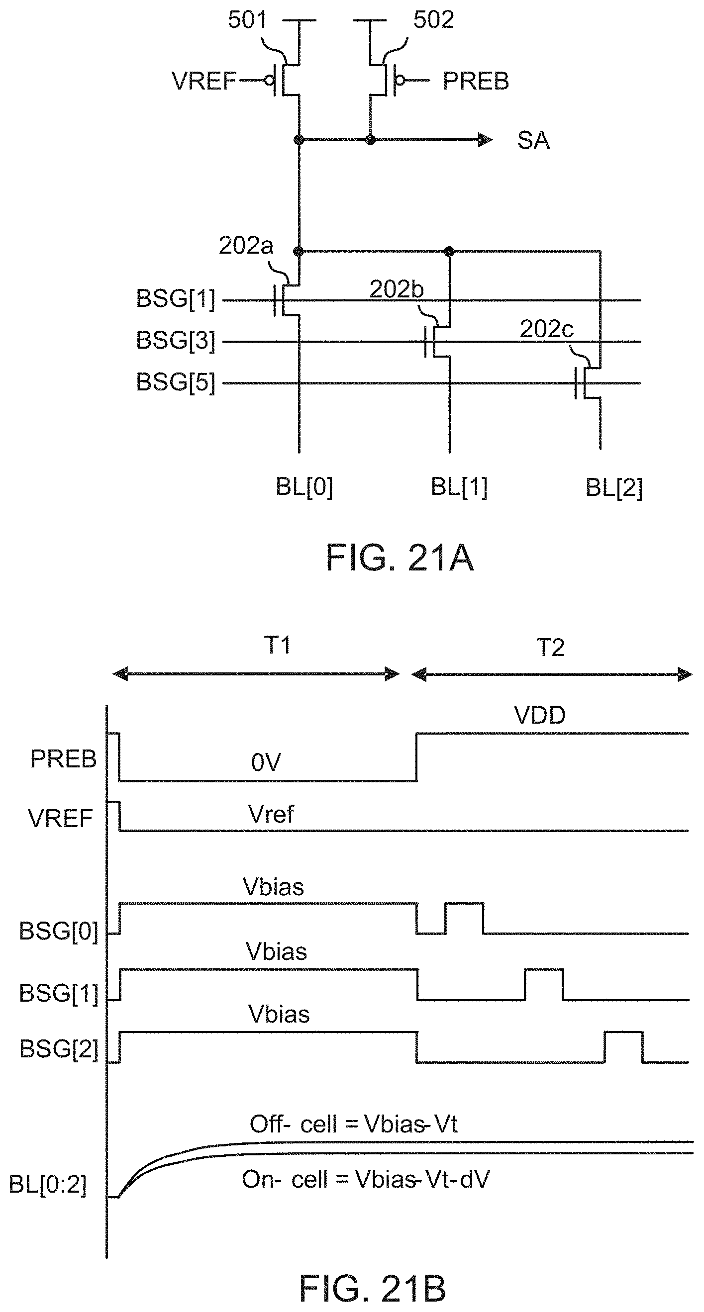
D00053
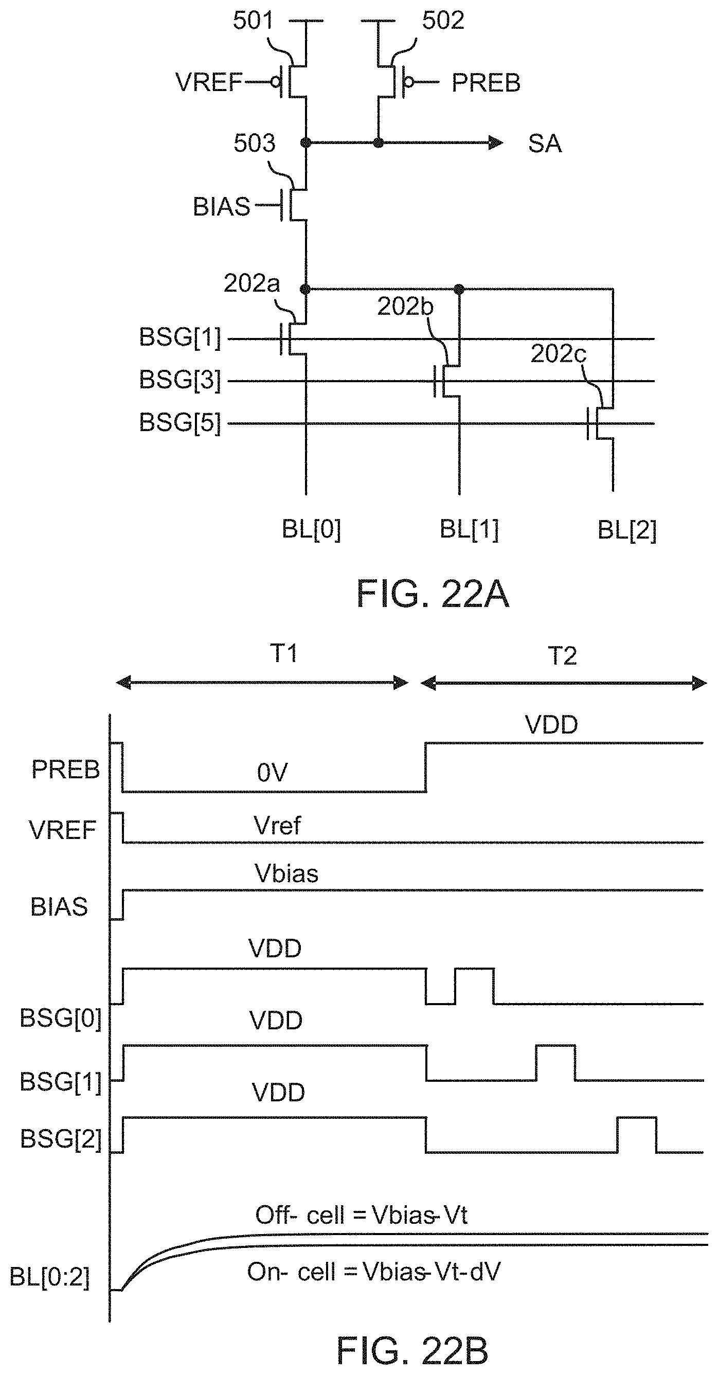
D00054
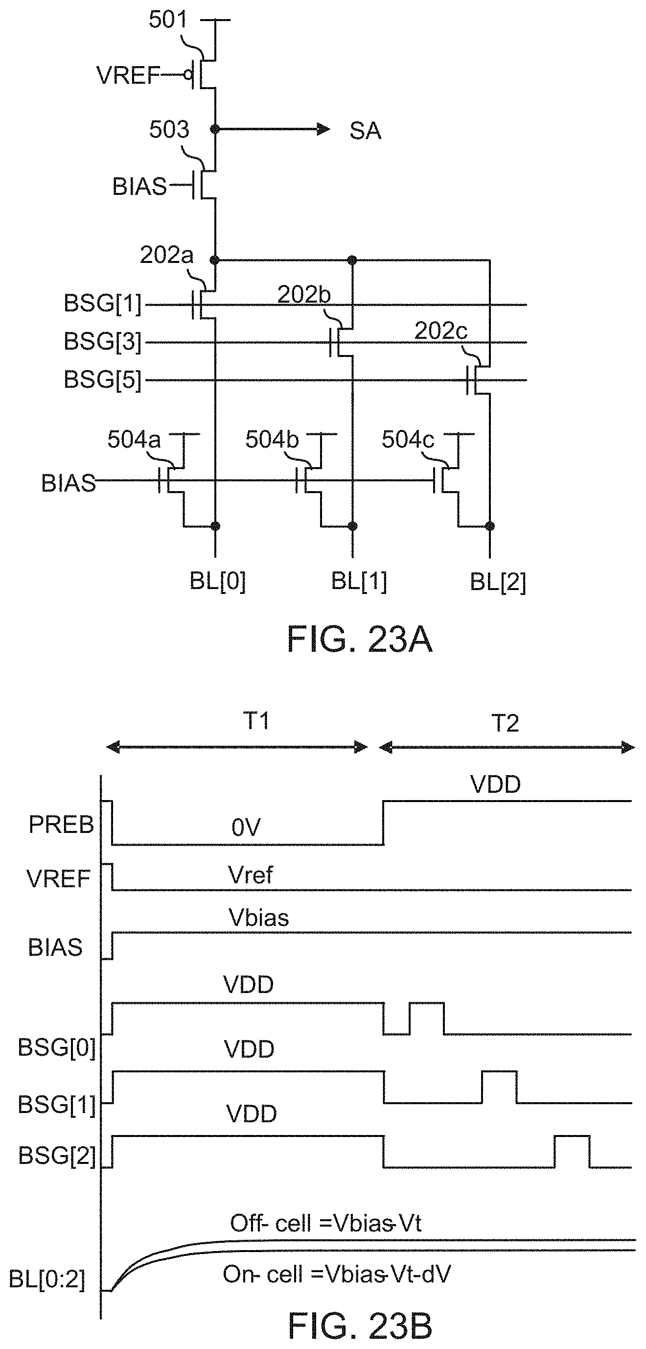
D00055
D00056
D00057
D00058

D00059
XML
uspto.report is an independent third-party trademark research tool that is not affiliated, endorsed, or sponsored by the United States Patent and Trademark Office (USPTO) or any other governmental organization. The information provided by uspto.report is based on publicly available data at the time of writing and is intended for informational purposes only.
While we strive to provide accurate and up-to-date information, we do not guarantee the accuracy, completeness, reliability, or suitability of the information displayed on this site. The use of this site is at your own risk. Any reliance you place on such information is therefore strictly at your own risk.
All official trademark data, including owner information, should be verified by visiting the official USPTO website at www.uspto.gov. This site is not intended to replace professional legal advice and should not be used as a substitute for consulting with a legal professional who is knowledgeable about trademark law.