Reduced and Pipelined Hardware Architecture for Montgomery Modular Multiplication
Carr; Ryan ; et al.
U.S. patent application number 16/184139 was filed with the patent office on 2020-05-14 for reduced and pipelined hardware architecture for montgomery modular multiplication. The applicant listed for this patent is Enveil, Inc.. Invention is credited to Michael J. Badamo, Ryan Carr.
| Application Number | 20200150930 16/184139 |
| Document ID | / |
| Family ID | 70550007 |
| Filed Date | 2020-05-14 |


| United States Patent Application | 20200150930 |
| Kind Code | A1 |
| Carr; Ryan ; et al. | May 14, 2020 |
Reduced and Pipelined Hardware Architecture for Montgomery Modular Multiplication
Abstract
A hardware implementations of Montgomery modular multiplication are described. The number of components as well as the number of cycles may be reduced by using a lookup table and multiplexer for selecting terms to be added during calculations. Also a loop unrolling technique may be used improve performance. A chain of pipeline adder modules and a chain of delay and shift modules may be used to pipeline calculations of multiple sets of operands.
| Inventors: | Carr; Ryan; (Fulton, MD) ; Badamo; Michael J.; (Rockville, MD) | ||||||||||
| Applicant: |
|
||||||||||
|---|---|---|---|---|---|---|---|---|---|---|---|
| Family ID: | 70550007 | ||||||||||
| Appl. No.: | 16/184139 | ||||||||||
| Filed: | November 8, 2018 |
| Current U.S. Class: | 1/1 |
| Current CPC Class: | G06F 7/728 20130101; G06F 7/727 20130101; G06F 7/722 20130101 |
| International Class: | G06F 7/72 20060101 G06F007/72 |
Claims
1. A hardware adder for performing Montgomery modular multiplication, the adder comprising: a first operand register for receiving a first operand, second operand register for receiving a second operand, and modulus register for receiving a modulus, and a sum register for receiving a sum of the second operand and the modulus; a first shift register configured for receiving the first operand from the first operand register and shifting the first operand; a second shift register configured to shift a result of a previous cycle; a multiplexer for selecting one of a zero, the modulus, the second operand, or the second operand and modulus sum, responsive to a predetermined bit of the second operand, a bit shifted out of the first shift register, and a predetermined bit of the current result; an adder configured to receive a selection from the multiplexer and a shifted previous result from the second shift register and output a current result; and a result accumulator to receive the result from the adder and output the current result to the second shift register as a previous result.
2. The hardware adder of claim 1, further comprising a second multiplexer for selecting one of the second shift register output and the second operand for output to the adder, the second multiplexer configured for initializing the sum register with the sum of the second operand and the modulus.
3. The hardware adder of claim 1, further comprising a controller including logic configured to: receive input including the bit received from the second operand, the bit shifted out of the first shift register, and the predetermined bit received from the current result; and provide a MUX select word to the multiplexer based on the received input, the select word used for selecting one of zero, the modulus, the second operand, or the second operand and modulus sum.
4. The hardware adder of claim 3, wherein the controller includes a lookup table.
5. The hardware adder of claim 4, wherein inputs of the lookup table include the bits received from the second operand, the shift register, and the result accumulator, and wherein outputs of the lookup table include MUX select words.
6. The hardware adder of claim 5, wherein the lookup table is a matrix, the matrix columns comprising: a first column ("B") representing second operand bit inputs, ("B"); a second column ("A") representing first shift register bit inputs; a third column ("R") representing result accumulator bit inputs; and a fourth column ("MUX") representing two bit MUX select word outputs; and the matrix rows comprising: TABLE-US-00005 B A R MUX 0 0 0 00 0 0 1 01 0 1 0 10 0 1 1 11 1 0 0 00 1 0 1 01 1 1 0 11 1 1 1 10.
7. The hardware adder of claim 5, wherein the lookup table is a matrix, the matrix columns comprising: a first column ("B") representing second operand bit inputs; a second column ("A") representing first shift register bit inputs; a third column ("R") representing result accumulator bit inputs; and a fourth column ("MUX select") representing an operand selected using the MUX select word outputs; and the matrix rows comprising: TABLE-US-00006 B A R MUX select 0 0 0 zero 0 0 1 modulus 0 1 0 second operand 0 1 1 sum of second operand and modulus 1 0 0 zero 1 0 1 modulus 1 1 0 sum of second operand and modulus 1 1 1 second operand.
8. A system for pipelining Montgomery modular multiplication, the system comprising: a first operand register for receiving a first operand (A), second operand register for receiving a second operand (B), and modulus register for receiving a modulus (M), and a sum register for receiving a sum of the second operand and the modulus (sum M+B); a first shift register configured for receiving the received operand A and shifting out a plurality of bits of A; a second shift register configured to receive a result of a plurality of bits and output a shifted result; a plurality of pipeline adders chained together such that the first pipeline adder receives the shifted result from the second shift register, and each of a plurality of the subsequent pipeline adders receives a result of a previous pipeline adder, each pipeline adder comprising: a multiplexer for selecting one of a zero, M, B, or sum M+B, responsive to a plurality of bits selected from each of B, the first shift register, and the current result, and an adder configured to add the received result to the selection from the multiplexer and output a result to the next pipeline adder in the chain; and a plurality of delay modules chained together, the first delay module configured to receive values including sum M+B, B, and M, and delay and shift the received values for output to a subsequent pipeline adder and delay module, each subsequent delay module configured to receive the delayed and shifted values from the previous delay module, and further delay and shift the received delayed and shifted values for output the to a subsequent delay module; and a result accumulator configured to receive the result from the final pipeline adder in the chain, and output the result to the second shift register.
9. The system of claim 8, further comprising an adder control module including logic configured to receive a plurality of bits from M, a plurality of bits from B, the plurality of bits shifted out of the first register and a plurality of bits from the result accumulator.
10. The system of claim 9, wherein the chain of pipeline adders includes 4 pipeline adders and the plurality of bits received from M are bits 3:1, the plurality of bits received from B are bits 3:0, the plurality of bits received from the first shift register are bits 3:0 and the plurality of bits received from the result accumulator are bits 7:4.
11. The system of claim 9, wherein the adder control module includes a plurality of lookup tables.
12. The system of claim 9, wherein the lookup tables are stored in read only memory.
13. A hardware circuit configured for performing a method of calculating a result of Montgomery modular multiplication, the hardware circuit including a multiplexer, a shift register, an adder, and a plurality of registers, the method comprising: receiving operand A at a first register of the hardware circuit, operand B at a second register of the hardware circuit, and a modulus M at a third register of the hardware circuit; setting a result value R in a result register of the hardware circuit to 0; initializing a value of a loop counter i in an index register to 0 initializing an end of loop value to n; 1) if a.sub.0 equals 0 and r.sub.0 equals 0, then: dividing (R+0) by 2, and placing the result of the division in the result register; 2) if a.sub.0 equals 0 and r.sub.0 equals 1, then: dividing (R+M) by 2, and placing the result of the division in the result register; 3) if a.sub.0 equals 1 and b.sub.0 equals r.sub.0, then: dividing (R+B) by 2, and placing the result of the division in the result register; 4) if a.sub.0 equals 1 and b.sub.0 is not equal to r.sub.0, then: dividing (R+M+B) by 2, and placing the result in the result register; 5) dividing A by 2; 6) placing the result of the division of A by 2 in the first register; adding 1 to i and placing the result of the addition in the index register if i is less than n, returning to step 1; and if R is greater than M then: subtracting M from R, and placing the result in the result register.
14. The hardware circuit of claim 13, wherein n is equal to a number of bits in the first register.
15. The hardware circuit of claim 13, further comprising: using the multiplexer and adder to determine which of addition steps to perform in steps 1-4; and using the shift register to perform the division in steps 1-4.
16. The hardware circuit of claim 13, further comprising using the hardware multiplexer and a lookup table to in steps 1-4 to determine which of the addition steps to perform.
17. The hardware circuit of claim 16, wherein the lookup table is a matrix, the matrix including columns comprising: a first column representing second operand bit inputs, ("B"); a second column representing first shift register bit inputs, ("A"); a third column representing result accumulator bit inputs, ("R"); and a forth column representing two bit MUX select word outputs ("MUX"); and the matrix including rows comprising: TABLE-US-00007 B A R MUX 0 0 0 00 0 0 1 01 0 1 0 10 0 1 1 11 1 0 0 00 1 0 1 01 1 1 0 11 1 1 1 10.
18. The hardware circuit of claim 13, wherein the hardware circuit is a field programmable gate array.
19. A device for performing Montgomery modular multiplication, the device comprising: a first register for receiving a operand A, second register for receiving operand B, a third register for receiving a modulus M, and a sum register for receiving a sum M+B; a first shift register configured for receiving A from the first register and repeatedly shifting a.sub.0 of A out of the first shift register; a second shift register configured to shift a result R and output R div 2; a multiplexer for performing a selection of one of 0, M, B, or M+B based on a received select word; an adder configured to: receive the selection of one of 0, M, B, or M+B from the multiplexer, receive R div 2 from the second shift register, and add R div 2 to the received selection; a result accumulator to receive a result R of the addition from the adder and output the result R to the second shift register; and a controller including: logic configured to receive b.sub.0, a.sub.0, and r.sub.1, and output a select word to the multiplexer; and a lookup table: inputs of the lookup table being the received b.sub.0, a.sub.0, and r.sub.1, output of the lookup table being the select word.
20. The device of claim 19, wherein the lookup table is a matrix, the matrix columns comprising: a first column ("B") representing second operand bit inputs; a second column ("A") representing first shift register bit inputs; a third column ("R") representing result accumulator bit inputs; and a fourth column ("MUX") representing two bit MUX select word outputs; and the matrix rows comprising: TABLE-US-00008 B A R MUX 0 0 0 00 0 0 1 01 0 1 0 10 0 1 1 11 1 0 0 00 1 0 1 01 1 1 0 11 1 1 1 10.
Description
FIELD OF THE PRESENT TECHNOLOGY
[0001] The present disclosure relates to the technical field of hardware encryption and decryption systems and methods. More particularly, the present invention is in the technical field of Montgomery Modular Multiplication using hardware architecture and very large scale integrated circuits such as FPGAs.
BACKGROUND
[0002] Modular exponentiation is a mathematical operation of the following form:
R=B.sup.E mod M
where the result R, base B, exponent E, and modulus M are all integers. A modular exponentiation is computed using a series of modular multiplications, using the property that
B.sup.XB.sup.Y=B.sup.X-Y
to build from the input B up to the desired exponentiation B.sup.E.
[0003] Modular exponentiation may be used by encryption systems such as homomorphic cryptosystems and an RSA encryption scheme. For example, RSA uses a modular exponentiation to perform both encryption and decryption: for encryption, B is the plaintext, E and M are parts of the public key, and R is the resulting ciphertext; for decryption, B is the ciphertext, E is the private key, M is part of the public key, and R is the resulting plaintext.
[0004] The performance of such cryptosystems depends on the implementation efficiency of the modular multiplication and exponentiation. The operands include plain text of a message, the cipher, and/or possibly a partially ciphered text. Operands are generally larger than word sizes in typical computer processor architecture. For example, operands can be 128-1024-bit words or more, whereas a typical processor may use 32- or 64-bit words. The time requirements for encryption/decryption operations using modular exponentiation may be reduced by reducing the number of modular multiplications performed and/or by reducing the time requirements to perform a single modular multiplication. Using hardware implementations for cryptosystems instead of software implementations can reduce the number of operations, for example, by designing hardware that can perform operations on word sizes larger than word sizes used in typical computers. However, increasing the word size in hardware also increases the device count in the integrated circuits, which increases complexity and cost.
SUMMARY
[0005] Various embodiments of the present technology include a hardware adder configured for performing Montgomery modular multiplication. The hardware adder further includes a first operand register for receiving a first operand, second operand register for receiving a second operand, and modulus register for receiving a modulus, and a sum register for receiving a sum of the second operand and the modulus; a first shift register configured for receiving the first operand from the first operand register and shifting the first operand; and a second shift register configured to shift a result of a previous cycle. The hardware adder further includes a multiplexer for selecting one of a zero, the modulus, the second operand, or the second operand and modulus sum, responsive to a predetermined bit of the second operand, a bit shifted out of the first shift register, and a predetermined bit of the current result; an adder configured to receive a selection from the multiplexer and a shifted previous result from the second shift register and output a current result; and a result accumulator to receive the result from the adder and output the current result to the second shift register as a previous result.
[0006] Various embodiments of the present technology include a system for pipelining Montgomery modular multiplication. The system includes a first operand register for receiving a first operand (A), second operand register for receiving a second operand (B), and modulus register for receiving a modulus (M), and a sum register for receiving a sum of the second operand and the modulus (sum M+B); a first shift register configured for receiving the received operand A and shifting out a plurality of bits of A; and a second shift register configured to receive a result of a plurality of bits and output a shifted result. The system further includes a plurality of pipeline adders chained together such that the first pipeline adder receives the shifted result from the second shift register, and each of a plurality of the subsequent pipeline adders receives a result of a previous pipeline adder, each pipeline adder comprising: a multiplexer for selecting one of a zero, M, B, or sum M+B, responsive to a plurality of bits selected from each of B, the first shift register, and the current result, and an adder configured to add the received result to the selection from the multiplexer and output a result to the next pipeline adder in the chain. The system also includes a plurality of delay modules chained together. The first delay module may be configured to receive values including sum M+B, B, and M, and delay and shift the received values for output to a subsequent pipeline adder and delay module. Each subsequent delay module may be configured to receive the delayed and shifted values from the previous delay module, and further delay and shift the received delayed and shifted values for output the to a subsequent delay module. The system also includes a result accumulator configured to receive the result from the final pipeline adder in the chain, and output the result to the second shift register.
[0007] Various embodiments of the present technology include a hardware circuit configured for performing a method of calculating a result of Montgomery modular multiplication, the hardware circuit including a multiplexer, a shift register, an adder, and a plurality of registers, the method comprising receiving operand A at a first register of the hardware circuit, operand B at a second register of the hardware circuit, and a modulus M at a third register of the hardware circuit and setting a result value R in a result register of the hardware circuit to 0. The method further includes initializing a value of a loop counter i in an index register to 0, and initializing an end of loop value to n. The method also includes steps of
[0008] 1) if a.sub.0 equals 0 and r.sub.0 equals 0, then: dividing (R+0) by 2, and placing the result of the division in the result register;
[0009] 2) if a.sub.0 equals 0 and r.sub.0 equals 1, then: dividing (R+M) by 2, and placing the result of the division in the result register;
[0010] 3) if a.sub.0 equals 1 and b.sub.0 equals r.sub.0, then: dividing (R+B) by 2, and placing the result of the division in the result register;
[0011] 4) if a.sub.0 equals 1 and b.sub.0 is not equal to r.sub.0, then: dividing (R+M+B) by 2, and placing the result in the result register;
[0012] 5) dividing A by 2; placing the result of the division of A by 2 in the first register; adding 1 to i and placing the result of the addition in the index register if i is less than n, returning to step 1.
[0013] The method further includes if R is greater than M then: subtracting M from R, and placing the result in the result register.
[0014] Various embodiments of the present technology include a device for performing Montgomery modular multiplication, the device comprising a first register for receiving a operand A, second register for receiving operand B, a third register for receiving a modulus M, and a sum register for receiving a sum M+B. The device further includes a first shift register configured for receiving A from the first register and repeatedly shifting a.sub.0 of A out of the first shift register; and a second shift register configured to shift a result R and output R div 2. The device also includes a multiplexer for performing a selection of one of 0, M, B, or M+B based on a received select word; and an adder configured to: receive the selection of one of 0, M, B, or M+B from the multiplexer, receive R div 2 from the second shift register, and add R div 2 to the received selection. The device further includes a result accumulator to receive a result R of the addition from the adder and output the result R to the second shift register; and a controller including: logic configured to receive b.sub.0, a.sub.0, and r.sub.1, and output a select word to the multiplexer; and a lookup table, inputs of the lookup table being the received b.sub.0, a.sub.0, and r.sub.1, output of the lookup table being the select word.
BRIEF DESCRIPTION OF THE DRAWINGS
[0015] Certain embodiments of the present technology are illustrated by the accompanying figures. It will be understood that the figures are not necessarily to scale and that details not necessary for an understanding of the technology or that render other details difficult to perceive may be omitted. It will be understood that the technology is not necessarily limited to the particular embodiments illustrated herein.
[0016] FIG. 1 is a block diagram illustrating a prior art hardware architecture for a Montgomery modular multiplier (MMM) architecture for implementation in hardware.
[0017] FIG. 2 illustrates details of a prior art controller of FIG. 1.
[0018] FIG. 3 is a block diagram illustrating a reduced MMM architecture, in accordance with aspects of the claimed technology.
[0019] FIG. 4 is a block diagram illustrating a loop unrolling technique using a pipeline architecture 400, in accordance with aspects of the claimed technology.
DETAILED DESCRIPTION
[0020] The terminology used herein is for the purpose of describing particular embodiments only and is not intended to be limiting of the present technology. As used herein, the singular forms "a", "an" and "the" are intended to include the plural forms as well, unless the context clearly indicates otherwise. It will be further understood that the terms "comprises" and/ or "comprising," when used in this specification, specify the presence of stated features, integers, steps, operations, elements, and/or components, but do not preclude the presence or addition of one or more of the same or other features, integers, steps, operations, elements, components, and/or groups thereof.
[0021] It will be understood that like or analogous elements and/or components referred to herein may be identified throughout the drawings with like reference characters. It will be further understood that several of the figures are merely schematic representations and/or block diagrams of the present technology. As such, some of the components may have been distorted from their actual scale for pictorial clarity.
[0022] In the present disclosure, the terms "lowest significant bit," "LSB," "bit 0" are used interchangeably. The terms "a.sub.0," "b.sub.0," "c.sub.0," . . . and so on refer to bit 0 or the LSB of terms "A," "B," "C," . . . and so on, respectively. Similarly bit 1, bit 2, bit 3 . . . of A may be written as "a.sub.1," "a.sub.2," "a.sub.3," . . . Bits 4-7 of A may be written as "A7:4". The terms "multiplexer" and "MUX" are used interchangeably.
[0023] The present technology reduces the number of operations and the device count in hardware cryptosystems. This may be accomplished by reducing the number of steps to perform multiplications and using pipelining.
[0024] An RSA cryptosystem includes three items: an integer modulus (M) of around 1024 bits, as well as an integer d and an integer e. Integer d may be referred to as a private key, while the pair (e, M) may be referred to as a public key. These items may satisfy the property
T.sup.de=T mod M.
[0025] The plain text T may obey the condition that 0.ltoreq.T<M. Messages may be encrypted using the public key as
C=T.sup.e mod M
[0026] Encrypted messages may be decrypted using the private key as
T=C.sup.d mod M.
[0027] So the same operation, modular exponentiation, may be used to perform both encryption and decryption.
[0028] A modular exponentiation is computed using a series of modular multiplications. Modular multiplication generally consists of two steps: one step generates a product
P=AB
and the other step reduces this product P modulo M.
[0029] The Montgomery form (also called Montgomery representation) of some number A mod M is equal to AP mod M, where r is the radix used to represent M and r.sup.i>M. For example, if M is a 1024-bit binary number then r=2 and i=1024 is valid.
[0030] An efficient algorithm for implementing a series of modular multiplications is to convert the first operands to Montgomery form, perform the multiplications using the Montgomery multiplication algorithm, and then convert the result out of Montgomery form. Montgomery multiplication takes the Montgomery representation of two operands A and B, and produces the Montgomery representation of AB mod M. Montgomery multiplication is faster than a standard modular multiplication because it does not require the division by M that is required to compute the modulus. Instead, it generates a reduced product using a series of additions.
[0031] Let operands A be the multiplicand, B the multiplicator, and M the modulus. Also let n be the number of bits, or digits in their binary representation, i.e. the radix is 2. So, we may denote A, B and M as follows:
A = i = 0 n a i .times. 2 i ##EQU00001## B = i = 0 n b i .times. 2 i ##EQU00001.2## M = i = 0 n m i .times. 2 i ##EQU00001.3##
[0032] Conditions for the Montgomery algorithm include a modulus M relatively prime to the radix (no common divisor for M and the radix) and M larger than the multiplicand and the multiplicator. Using a binary representation of the operands requires the modulus M to be odd to satisfy the first condition (relatively prime). The operands A and B must also be in Montgomery form.
[0033] The Montgomery algorithm may use the least significant digit of the accumulating modular partial product to determine the multiple of M to subtract. The usual multiplication order is reversed by choosing multiplier digits from least significant to most significant and shifting down. Representing the current modular partial product as R, q is chosen so that R+qM is a multiple of the radix r, which is right-shifted, i.e. divided by r for use in the next iteration. After n iterations, the result obtained is:
R=AB*mod M
[0034] Table 1 illustrates a version of a Montgomery algorithm.
TABLE-US-00001 TABLE 1 algorithm Montgomery(A, B, M) { int R = 0; 1: for i = 0 to n { 2: R = R + a.sub.iB; 3: if r.sub.0 = 0 then 4: R = R div 2 5: else 6: R = (R + M) div 2; } return R; }
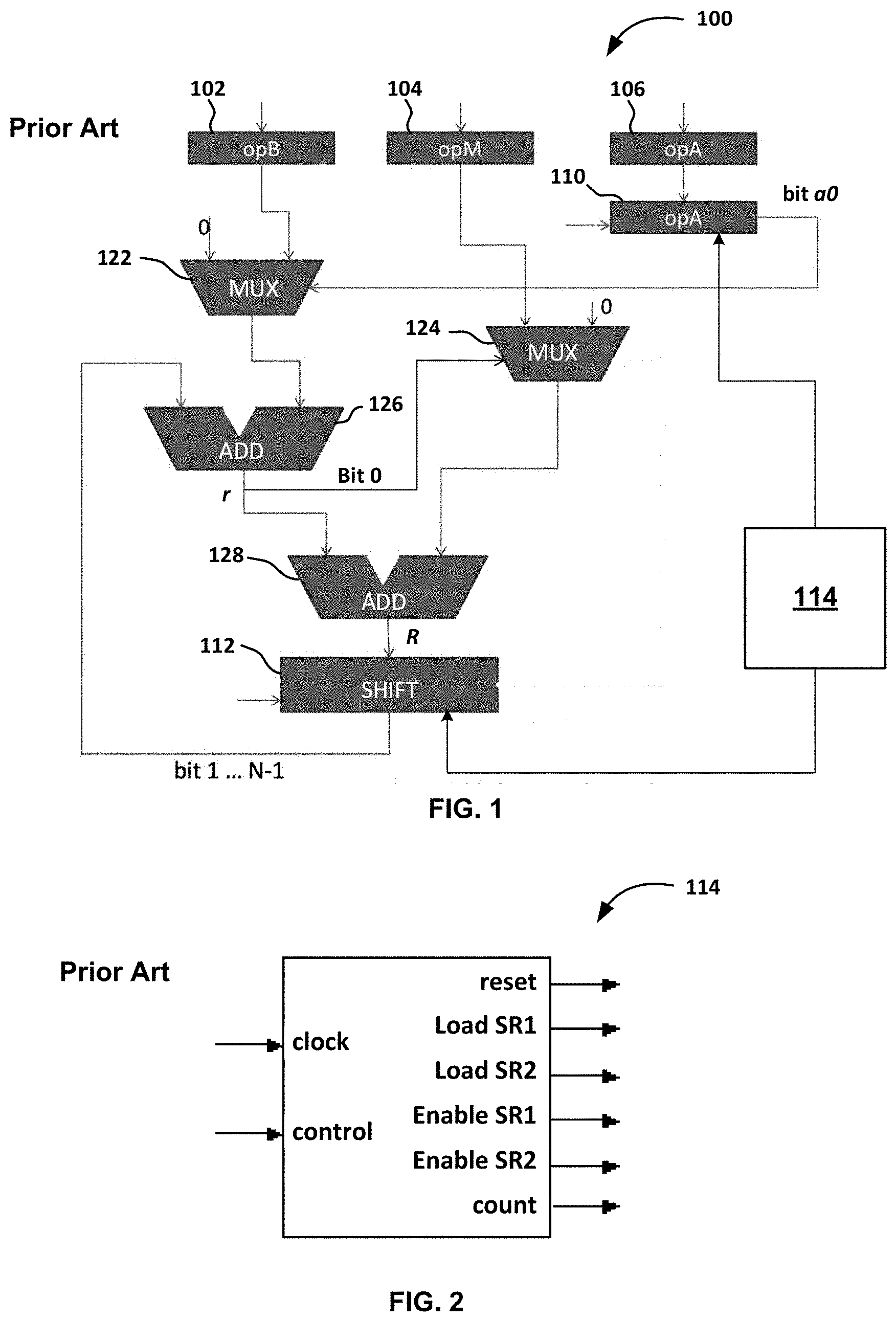
[0035] FIG. 1 is a block diagram illustrating a prior art hardware architecture for a Montgomery modular multiplier (MMM) architecture 100 for implementation in hardware. In various embodiments, the MMM architecture 100 is implemented in Field Programmable Gate Array (FPGA), Application Specific Integrated Circuits, Very Large Scale Integrated Circuits, and/or the like. The MMM architecture 100 of FIG. 1 is configured to receive operands A, B and M and it return
R=(A.times.B.times.2.sup.-n mod M
[0036] The MMM architecture 100 includes two multiplexers (MUX 122 and MUX 124), two adders (ADD 126 and ADD 128), two shift registers (SHIFT 110 and SHIFT 112), three input registers (opB 102, opM 104, and opA 106) as well as a controller 114, described in more detail in FIG. 2.
[0037] The first multiplexer, MUX 122 passes a value of 0 when the LSB, or bit 0 shifted out of the shift register 110, bit a.sub.0, is 0, and passes the content of register opB 102 when LSB of a.sub.0 shifted out of the first shift register 110 is 1. The second multiplexer, MUX 124 passes a value of 0 or the content of register opM 104 depending on whether the LSB of a result r of adder ADD 126, bit r.sub.0, is a 0 or 1, respectively.
[0038] The first adder, ADD 126, outputs the sum R+a.sub.i.times.B (line 2 of algorithm of Table 1), where i is the iteration number. The second adder, ADD 128 outputs the sum R+M (line 6 of the same algorithm in Table 1). The first shift register, SHIFT 110 provides the bit a.sub.i. At each iteration of the multiplier, this shift register is right-shifted once so that a.sub.0 contains a.sub.i of the original A operand.
[0039] More generally, the operands A and B and Modulus M are fed into the input registers marked opA 106, opB 102, and opM 104, respectively. Multiplexers MUX 122 and MUX 124 control which operands are combined with the intermediate result for each iteration using the adders ADD 126 and 128, and the shift register SHIFT 112 to store the intermediate result. The hardware performs one iteration per bit in operand A. The LSB of the shifted operand opA 110 determines whether operand opB, is added to the result. The LSB of that sum r determines whether operand opM is added to that sum r. The result R is shifted by one bit (marked "bit 1 . . . N-1") in the SHIFT 112 register, that value may be applied to an input of the first adder ADD 126 for the next iteration.
[0040] FIG. 2 illustrates details of a prior art controller 114 of FIG. 1. The controller 114 may be used to synchronize shifting and loading operations of the first shift register SHIFT 110. The controller 114 may also control a number of iterations to be performed by the multiplier, using a simple down counter (not illustrated).
[0041] In order to synchronize the work of the components of the architecture 100, the controller 114 includes a state machine, which may have 6 states as illustrated in Table 2.
TABLE-US-00002 TABLE 2 State Actions S0: initialization of the state machine; set counter = n go to S1 S1: load multiplicand and modulus into registers; load multiplicator into shift register1; go to S2; S2: wait for ADDER1; wait for ADDER2; load multiplicator into shift register2; decrement counter; go to S3; S3: enable shift register2; enable shift register1; S4: check the counter; if 0 then go to S5 else go to S2; S5: halt;
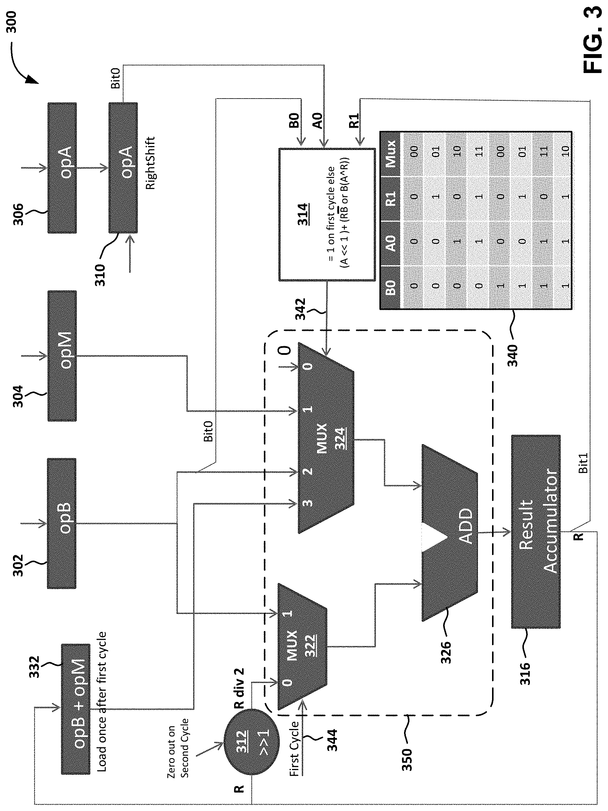
[0042] In the course of developing the claimed technology, it has been determined that the number of cycles can be reduced by eliminating an adder from the MMM architecture 100 illustrated in FIG. 1. Furthermore, device count may also be reduced.
[0043] FIG. 3 is a block diagram illustrating a reduced MMM architecture 300, in accordance with aspects of the claimed technology. In various embodiments, the reduced MMM architecture 300 is implemented in FPGAs, Application Specific Integrated Circuits, Very Large Scale Integrated Circuits, and/or the like. The reduced MMM architecture 300 includes a first multiplexer MUX 324, a second multiplexer MUX 322, an adder ADD 326, a first shift register opA 310, a divide by 2 function (R div 2 function) 312, a result accumulator 316), a controller 314, and three input operand registers (opB 302, opM 304, and opA 306). It is noteworthy that the term "accumulator" is a simple register. The label "accumulator" refers to the purpose it serves in conjunction with the adder 326 from iteration to iteration. It is also noteworthy that the output of the accumulator 316 may be guaranteed to enter the adder 326 after the first two iterations.
[0044] On the first cycle, a value of 1 is applied to the select input of MUX 322. Also on the first cycle, the controller 314 is configured to apply a value of 1 to the select word 342 input to the MUX 324. In some embodiments, the controller sets the value applied to the select inputs 344 of the MUX 322. Thus, the control input for both the first and second and multiplexers (MUX 322 and MUX 324) is set to 1 on the first cycle. As a result, on the first cycle B is passed from MUX 322 and M is passed from MUX 324 to the adder ADD 326. The adder 326 generates an intermediate result B+M, which may then be loaded to a register 332 upon completion of the first cycle. The register 332 is loaded only once to store the sum B+M for use in later cycles. Since the first cycle is used to load the sum B+M to the register 332, the R div 2 function 312 may be zeroed out on the second cycle so that a 0 is passed to the adder on the second cycle, which begins the MMM calculation. In all other cycles the control bit for the MUX 322 is 0, and a right shifted result from the R div 2 function 312 is applied to the MUX 322, 0 input and passed to the adder 326.
[0045] In some embodiments, the controller 314 is used to control when to load the sum B+M to the register 332. The controller 314 may also be used to control when to zero out the R div 2 function 312. The controller 314 may further be used for controlling timing for loading opA into the first shift register 310 and shifting bits of A out of the first shift register 310. The controller 314 may also be used for loading a result from the result accumulator 316, and outputting the shifted result from the R div 2 function 312 to the MUX 322.
[0046] On completion of the second and subsequent cycles, the R div 2 function 312 receives the result R from the result accumulator 316 and presents a result R that is shifted 1 bit (or R div 2) to the MUX 322. The MUX 322 then passes R div 2 to the adder 326 for the next cycle.
[0047] The adder 326 then adds R div 2 from the MUX 322 to one of 0, M, B, or B+M from the MUX 324, depending on the output of the controller 314. The output of the controller 314 is placed on the select word 342 for input to the MUX 324. The select word 342 includes at least two bits. The output of the controller 314 to the select word 342 is based on the inputs, b.sub.0 (bit 0 of B), a.sub.0 (bit 0 of shift register 310), and n (bit 1 of result accumulator 316). In some embodiments, the controller 314 includes a lookup table 340 that is used for determining the output based on b.sub.0, a.sub.0, and n. The controller 314 may also control a number of iterations to be performed by the multiplier, for example, by using a simple down counter (not illustrated).
[0048] Table 3 below is an algorithm for describing a process of for determining whether to add 0, M, B, or M+B to the result R, using the circuit illustrated in FIG. 3 and based on the lookup table 340.
TABLE-US-00003 TABLE 3 Intermediate Algorithm 1: Inputs(A, B, M) int R = 0; intS = B + M; for i = 0 to n { if a.sub.0 == 0 then if r.sub.0 == 0 then 1) R' = R else 2) R' = (R + M) else if b.sub.0 == r.sub.0 then 3) R' = (R + B) else 4) R' = (R + S) A = A div 2 R = R' div 2 } 5) if R > M then 6) R = R - M return R
[0049] At step 1) of the algorithm in Table 3, a.sub.0=0, r.sub.0=0. The value 0 is selected by the MUX 324, which results in adding 0 to the result of the previous iteration (labelled R in Table 3 and R div 2 in FIG. 3) according to the lookup table 340. In the pseudo-code of Table 3, r.sub.0 refers to the LSB of R after the shift in R div 2 function 312 from the previous iteration has occurred. However, in FIG. 3, R1 is labeled as the result as it leaves the accumulator prior to the shift in R div 2 function 312, so the relevant bit is r.sub.1.
[0050] At step 2) of the algorithm in Table 3, a.sub.0=0, r.sub.0=1. M in the register 304 is selected by the MUX 324, which results in adding M to the result of the previous iteration based on the lookup table 340.
[0051] At step 3) of the algorithm in Table 3, a.sub.0=1, b.sub.0=r.sub.0. B in the register 302 is selected by the MUX 324, which results in adding B to the result of the previous iteration, based on the lookup table 340.
[0052] At step 4) of the algorithm in Table 3, a.sub.0=1, b.sub.0.noteq.r.sub.0. B+M in the register 332 is selected by the MUX 324, which results in adding B+M (S) to the result of the previous iteration, based on the lookup table 340.
[0053] Steps 5 and 6 account for a condition that when the for loop completes, R is between M and 2M. Steps 5 and 6 serve to check if this is the case and correct it if so.
[0054] The dotted line 350 indicates elements of a pipeline adder that includes the MUX 322, the MUX 324 and the adder 326 of FIG. 3. The pipeline adder 350 may be used as a component of a pipeline architecture to add one of at least four different values to the input R value (i.e., 0, B, M, (M+B)), as described in greater detail elsewhere herein.
[0055] FIG. 4 is a block diagram illustrating a loop unrolling technique using a pipeline architecture 400, in accordance with aspects of the claimed technology. In various embodiments, the pipeline architecture 400 is implemented in FPGAs, Application Specific Integrated Circuits, Very Large Scale Integrated Circuits, and/or the like. In FIG. 4, there are 32 sets of operands A, B, and M that may be pipelined, instead of just calculating one set of operands at a time. The four pipeline adders 350A-D of FIG. 4 may be chained as illustrated as pipeline adders 350A-D. Each pipeline adder 350A-D of FIG. 4 is chained using shift/delay registers 452B, 452C, and 452D to shift and delay inputs of the operands M+B, B, and M, into each step.
[0056] Similar to the controller 314 of FIG. 3, an Adder Control Decode ROM 414 may perform logic used to switch between adding 0, B, M, and M+B (shifted as necessary) at each step. Inputs to the ROM 414 that are used for switching the MUX 324 of the pipeline adders 350A-D include bits 7:4 of the intermediate result R and the lowest 4 bits of operands A, B, and M. It is noteworthy that since operand M is always odd, the LSB is always 1. For this reason, FIG. 4 only shows bits 3:1 being applied to the ROM 414. Also, bits 7:4 of the intermediate result R will be the lowest bits after 4 shifts are performed in the next iteration. This process is described by Intermediate Algorithm 2 in Table 4 below.
[0057] Table 4 below is an algorithm for describing a process for performing the loop unrolling technique, using a circuit illustrated the block diagram of FIG. 4.
TABLE-US-00004 TABLE 4 Intermediate Algorithm 2: int R = 0; int S = B + M for i = 0; i < n; i += 4 { if a.sub.0 == 0 then if r.sub.0 == 0 then R' = R else R' = (R + M) else if b.sub.0 == r.sub.0 then R' = (R + B) else R' = (R + S) if a.sub.1 == 0 then if r.sub.1 == r'.sub.1 then R' = R' + 2 * R else R' = R' + 2 * (R + M) else if r'.sub.1 == 0 and b.sub.0 == r.sub.1 then R' = R' + 2 * (R + B) else R' = R' + 2 * (R + S) if a.sub.2 == 0 then if r.sub.2 == r'.sub.2 then R' = R' + 4 * R else R' = R' + 4 * (R + M) else if r'.sub.2 == 0 and b.sub.0 == r.sub.2 then R' = R' + 4 * (R + B) else R' = R' + 4 * (R + S) if a.sub.3 == 0 then if r.sub.3 == R'.sub.3 then R' = R' + 8 * R else R' = R' + 8 * (R + M) else if r'.sub.3 == 0 and b.sub.0 == r.sub.3 then R' = R' + 8 * (R + B) else R' = R' + 8 * (R + S) A = A div 16 R = R' div 16 } if R > M then R = R - M return R
[0058] It is noteworthy that a batch of 32 results may be generated using about 16448 cycles for the processing of a batch of 32 sets of operands A, B, and M, using the unrolled pipeline architecture 400. This is about four times as fast about 65600 cycles that it might take to generate a batch of results from processing the same batch of 32 sets of operands A, B, and M using the reduced MMM architecture 300.
[0059] For simplicity, only four stages (A-D) are illustrated in the pipeline architecture 400 of FIG. 4. However, it may be appreciated that more or fewer stages may be used in hardware such as FPGA's for implementing the unrolled pipeline architecture 400, although a different control calculation may be used. For example, an unrolled pipeline architecture 400 may be implemented using 8, 16, 32, 64, 128, 256, 512, 1024, or more stages. The number of stages is not limited to powers of 2.
[0060] The corresponding structures, materials, acts, and equivalents of any means or step plus function elements in the claims below are intended to include any structure, material, or act for performing the function in combination with other claimed elements as specifically claimed. The description of the present technology has been presented for purposes of illustration and description, but is not intended to be exhaustive or limited to the present technology in the form disclosed. Many modifications and variations will be apparent to those of ordinary skill in the art without departing from the scope and spirit of the present technology. Exemplary embodiments were chosen and described in order to best explain the principles of the present technology and its practical application, and to enable others of ordinary skill in the art to understand the present technology for various embodiments with various modifications as are suited to the particular use contemplated.
[0061] Aspects of the present technology are described above with reference to flowchart illustrations and/or block diagrams of methods, apparatus (systems) and computer program products according to embodiments of the present technology. It will be understood that each block of the flowchart illustrations and/or block diagrams, and combinations of blocks in the flowchart illustrations and/or block diagrams, can be implemented by computer program instructions. These computer program instructions may be provided to a processor of a general purpose computer, special purpose computer, or other programmable data processing apparatus to produce a machine, such that the instructions, which execute via the processor of the computer or other programmable data processing apparatus, create means for implementing the functions/acts specified in the flowchart and/or block diagram block or blocks.
[0062] These computer program instructions may also be stored in a computer readable medium that can direct a computer, other programmable data processing apparatus, or other devices to function in a particular manner, such that the instructions stored in the computer readable medium produce an article of manufacture including instructions which implement the function/act specified in the flowchart and/or block diagram block or blocks.
[0063] The computer program instructions may also be loaded onto a computer, other programmable data processing apparatus, or other devices to cause a series of operational steps to be performed on the computer, other programmable apparatus or other devices to produce a computer implemented process such that the instructions which execute on the computer or other programmable apparatus provide processes for implementing the functions/acts specified in the flowchart and/or block diagram block or blocks.
[0064] The flowchart and block diagrams in the Figures illustrate the architecture, functionality, and operation of possible implementations of systems, methods and computer program products according to various embodiments of the present technology. In this regard, each block in the flowchart or block diagrams may represent a module, segment, or portion of code, which comprises one or more executable instructions for implementing the specified logical function(s). It should also be noted that, in some alternative implementations, the functions noted in the block may occur out of the order noted in the figures. For example, two blocks shown in succession may, in fact, be executed substantially concurrently, or the blocks may sometimes be executed in the reverse order, depending upon the functionality involved. It will also be noted that each block of the block diagrams and/or flowchart illustration, and combinations of blocks in the block diagrams and/or flowchart illustration, can be implemented by special purpose hardware-based systems that perform the specified functions or acts, or combinations of special purpose hardware and computer instructions.
[0065] In the following description, for purposes of explanation and not limitation, specific details are set forth, such as particular embodiments, procedures, techniques, etc. in order to provide a thorough understanding of the present invention. However, it will be apparent to one skilled in the art with this disclosure before them that the present invention may be practiced in other embodiments that depart from these specific details.
[0066] Reference throughout this specification to "one embodiment" or "an embodiment" means that a particular feature, structure, or characteristic described in connection with the embodiment is included in at least one embodiment of the present invention. Thus, the appearances of the phrases "in one embodiment" or "in an embodiment" or "according to one embodiment" (or other phrases having similar import) at various places throughout this specification are not necessarily all referring to the same embodiment. Furthermore, the particular features, structures, or characteristics may be combined in any suitable manner in one or more embodiments. Furthermore, depending on the context of discussion herein, a singular term may include its plural forms and a plural term may include its singular form. Similarly, a hyphenated term (e.g., "co-located") may be occasionally interchangeably used with its non-hyphenated version (e.g., "co-located"), a capitalized entry (e.g., "Software") may be interchangeably used with its non-capitalized version (e.g., "software"), a plural term may be indicated with or without an apostrophe (e.g., PE's or PEs), and an italicized term (e.g., "N+1") may be interchangeably used with its non-italicized version (e.g., "N+1"). Such occasional interchangeable uses shall not be considered inconsistent with each other.
[0067] The terminology used herein is for the purpose of describing particular embodiments only and is not intended to be limiting of the invention. As used herein, the singular forms "a," "an," and "the" are intended to include the plural forms as well, unless the context clearly indicates otherwise. It will be further understood that the terms "comprises" and/or "comprising," when used in this specification, specify the presence of stated features, integers, steps, operations, elements, and/or components, but do not preclude the presence or addition of one or more other features, integers, steps, operations, elements, components, and/or groups thereof.
[0068] It is noted at the outset that the terms "coupled," "connected," "connecting," "electrically connected," etc., are used interchangeably herein to generally refer to the condition of being electrically/electronically connected. Similarly, a first entity is considered to be in "communication" with a second entity (or entities) when the first entity electrically sends and/or receives (whether through wireline or wireless means) information signals (whether containing data information or non-data/control information) to the second entity regardless of the type (analog or digital) of those signals. It is further noted that various figures (including component diagrams) shown and discussed herein are for illustrative purpose only, and are not drawn to scale.
[0069] While specific embodiments of, and examples for, the system are described above for illustrative purposes, various equivalent modifications are possible within the scope of the system, as those skilled in the relevant art will recognize. For example, while processes or steps are presented in a given order, alternative embodiments may perform routines having steps in a different order, and some processes or steps may be deleted, moved, added, subdivided, combined, and/or modified to provide alternative or sub-combinations. Each of these processes or steps may be implemented in a variety of different ways. Also, while processes or steps are at times shown as being performed in series, these processes or steps may instead be performed in parallel, or may be performed at different times.
[0070] While various embodiments have been described above, it should be understood that they have been presented by way of example only, and not limitation. The descriptions are not intended to limit the scope of the invention to the particular forms set forth herein. To the contrary, the present descriptions are intended to cover such alternatives, modifications, and equivalents as may be included within the spirit and scope of the invention as defined by the appended claims and otherwise appreciated by one of ordinary skill in the art. Thus, the breadth and scope of a preferred embodiment should not be limited by any of the above-described exemplary embodiments.
* * * * *
uspto.report is an independent third-party trademark research tool that is not affiliated, endorsed, or sponsored by the United States Patent and Trademark Office (USPTO) or any other governmental organization. The information provided by uspto.report is based on publicly available data at the time of writing and is intended for informational purposes only.
While we strive to provide accurate and up-to-date information, we do not guarantee the accuracy, completeness, reliability, or suitability of the information displayed on this site. The use of this site is at your own risk. Any reliance you place on such information is therefore strictly at your own risk.
All official trademark data, including owner information, should be verified by visiting the official USPTO website at www.uspto.gov. This site is not intended to replace professional legal advice and should not be used as a substitute for consulting with a legal professional who is knowledgeable about trademark law.