Method and Apparatus for Contact Image Sensing
Popovich; Milan Momcilo ; et al.
U.S. patent application number 16/743905 was filed with the patent office on 2020-05-14 for method and apparatus for contact image sensing. This patent application is currently assigned to DigiLens Inc.. The applicant listed for this patent is DigiLens Inc.. Invention is credited to Alastair John Grant, Milan Momcilo Popovich, Jonathan David Waldern.
| Application Number | 20200150469 16/743905 |
| Document ID | / |
| Family ID | 55967320 |
| Filed Date | 2020-05-14 |


View All Diagrams
| United States Patent Application | 20200150469 |
| Kind Code | A1 |
| Popovich; Milan Momcilo ; et al. | May 14, 2020 |
Method and Apparatus for Contact Image Sensing
Abstract
A contact image sensor comprises: a waveguiding structure for propagating light in a first direction comprising, in series, a first clad medium, a first core, a switchable grating clad, a second core, and a second clad medium sandwiched by transparent substrates, patterned parallel electrode elements orthogonally traversing the waveguides, a light source, a platen and a detector. Switchable grating regions overlapped by a first voltage-addressed electrode element diffract TIR light from the first core towards the platen. Switchable grating region overlapped by a second voltage-addressed electrode element diffract TIR light reflected from the platen into a TIR path within the second core.
| Inventors: | Popovich; Milan Momcilo; (Leicester, GB) ; Waldern; Jonathan David; (Los Altos Hills, CA) ; Grant; Alastair John; (San Jose, CA) | ||||||||||
| Applicant: |
|
||||||||||
|---|---|---|---|---|---|---|---|---|---|---|---|
| Assignee: | DigiLens Inc. Sunnyvale CA |
||||||||||
| Family ID: | 55967320 | ||||||||||
| Appl. No.: | 16/743905 | ||||||||||
| Filed: | January 15, 2020 |
Related U.S. Patent Documents
| Application Number | Filing Date | Patent Number | ||
|---|---|---|---|---|
| 15562755 | Sep 28, 2017 | 10591756 | ||
| PCT/GB2016/000065 | Mar 30, 2016 | |||
| 16743905 | ||||
| 62178041 | Mar 31, 2015 | |||
| Current U.S. Class: | 1/1 |
| Current CPC Class: | G02B 5/1828 20130101; G02F 1/1326 20130101; G02B 26/0808 20130101; G02B 27/4272 20130101; G02F 1/29 20130101 |
| International Class: | G02F 1/13 20060101 G02F001/13; G02B 27/42 20060101 G02B027/42; G02B 26/08 20060101 G02B026/08; G02B 5/18 20060101 G02B005/18; G02F 1/29 20060101 G02F001/29 |
Claims
1. A contact image sensor comprising: a waveguiding structure for propagating light in a first direction comprising, in series disposed in a layer sandwiched by transparent substrates, a first clad medium, a first core, a switchable grating clad, a second core, and a second clad medium; electrodes applied to opposing surfaces of said substrates at least one patterned into a set of parallel elements orthogonally traversing said cores; a light source optically coupled to said first and second cores; a platen in optical contact with said waveguiding structure; a detector optically coupled to said first and second core regions; wherein switchable grating regions overlapped by a first voltage-addressed electrode element are operative, in their diffracting state, to diffract TIR light from first core into a path to outer surface of said platen, wherein switchable gratings region overlapped by a second voltage-addressed electrode element are operative, in their diffracting state, diffract TIR light reflected from said platen into a TIR path to said detector along said second core.
2. The apparatus of claim 1 wherein said waveguiding structure comprises a multiplicity of said cores and said clads cyclically arranged.
3. The apparatus of claim 1 wherein said voltages are applied sequentially, two electrodes at a time, to all electrodes in the array.
4. The apparatus of claim 1 wherein said diffracting state exists when no electric field is applied across said SBG element and said non-diffracting state exists when an electric field is applied or said diffracting state exists when an electric field is applied across said SBG element and said non-diffracting state exists when no electric field is applied.
5. The apparatus of claim 1 wherein when contact is made with an external material at a region on said platen a portion of the light incident at the region on said platen contacted by said external material is transmitted out of said platen, wherein light incident on the outer surface of said platen in the absence of said contact with an external material is reflected downwards.
6. The apparatus of claim 1 wherein when contact is made with an external material at a region on said platen a portion of the light incident at the region on said platen contacted by said external material is reflected downwards, wherein light incident on the outer surface of said platen in the absence of said contact with an external material. is transmitted out of said platen.
7. The apparatus of claim 1 wherein the output from said detector is read out in synchronism with the switching of said electrode elements.
8. The apparatus of claim 1 wherein said light source is one of a laser or LED and said light is coupled into said waveguiding structure by one of a grating or a prism.
9. The apparatus of claim 1 wherein said grating or prism are clocked.
10. The apparatus of claim 1 wherein said switchable grating clad is a switchable Bragg grating recorded in one of a HPDLC grating, uniform modulation grating or reverse mode HPDLC grating.
11. The apparatus of claim 1 wherein said switchable grating clad includes at least one of a fold grating or a multiplexed grating or a rolled k-vector grating.
12. A method of making a contact image measurement comprising the steps of: a) providing a waveguiding structure for propagating light in a first direction comprising, in series disposed in a layer sandwiched by transparent substrates, a first clad medium, a first core, a switchable grating clad, a second core, and a second clad medium; electrodes applied to opposing surfaces of said substrates at least one patterned into a set of parallel elements orthogonally traversing said cores; a light source optically coupled to said first and second cores; a platen in optical contact with said waveguiding structure; a detector optically coupled to said first and second core regions; b) coupling said light into a TIR path in said waveguiding structure; c) an external material contacting a region on the external surface of said platen; d) setting first and second electrode elements to a first voltage state and all other voltage-addressed electrodes set to a second voltage state; e) switchable grating regions overlapped by a first electrode element diffracting TIR light from first core into a path to the platen outer surface; f) switchable grating regions overlapped by a second electrode element diffracting light reflected from one of said region or said platen external surface into a TIR path in said second core; g) transmitting said reflected light to said detector.
13. The method of claim 12 wherein said first voltage state corresponds to a voltage being applied and said second voltage state corresponds to no voltage being applied.
14. The method of claim 12 wherein said first voltage state corresponds to no voltage being applied and said second voltage state corresponds to a voltage being applied.
15. The method of claim 12 wherein at least a portion of said light incident at said region on said platen is transmitted out of said platen, wherein at least a portion of said second optical path light not incident at said region is reflected.
16. The method of claim 12 wherein at least a portion of said light incident at said region on said platen is reflected, wherein at least a portion of said second optical path light not incident at said region being transmitted out of said platen.
17. The apparatus of claim 12 wherein said waveguiding structure comprises a multiplicity of said cores and said clads cyclically arranged.
18. The apparatus of claim 12 wherein said voltages are applied sequentially, two electrodes at a time, to all electrodes in the array.
19. The apparatus of claim 1 wherein the output from detector is read out in synchronism with the switching of the electrode elements.
20. The apparatus of claim 1 configured as a finger print scanner or a touch sensor.
Description
CROSS REFERENCE TO RELATED APPLICATIONS
[0001] This application is a continuation of U.S. patent application Ser. No. 15/562,755 filed on Sep. 28, 2017, which is a U.S. National Phase of PCT Application No. PCT/GB2016/000065 filed on Mar. 30, 2016, which claims the benefit of U.S. Provisional Patent Application No. 62/178,041 filed Mar. 31, 2015, the disclosures of which are incorporated herein by reference in their entireties.
BACKGROUND OF THE INVENTION
[0002] The present invention relates to an imaging sensor, and more particularly to a contact image sensor using electrically switchable Bragg gratings.
[0003] A contact image sensor is an integrated module that comprises an illumination system, an optical imaging system and a light-sensing system--all within a single compact component. The object to be imaged is place in contact with a transparent outer surface (or platen) of the sensor. Well known applications of contact image sensors include document scanners, touch sensors for computer interfaces, bar code readers and optical identification technology. Another field of application is in biometric sensors, where there is growing interest in automatic finger print detection. Fingerprints are a unique marker for a person, even an identical twin, allowing trained personel or software to detect differences bewtween individuals. Fingerprinting using the traditional method of inking a finger and applying the inked finger to paper can be extremely time-consuming. Digital technology has advanced the art of fingerprinting by allowing images to be scanned and the image digitized and recorded in a manner that can be searched by computer. Problems can arise due to the quality of inked images. For example, applying too much or too little ink may result in blurred or vague images. Further, the process of scanning an inked image can be time-consuming. A better approach is to use "live scanning" in which the fingerprint is scanned directly from the subject's finger. More specifically, live scans are those procedures which capture fingerprint ridge detail in a manner which allows for the immediate processing of the fingerprint image with a computer. Examples of such fingerprinting systems are disclosed in Fishbine et al. (U.S. Pat. Nos. 4,811,414 and 4,933,976); Becker (U.S. Pat. No. 3,482,498); McMahon (U.S. Pat. No. 3,975,711); and Schiller (U.S. Pat. Nos. 4,544,267 and 4,322,163). A live scanner must be able to capture an image at a resolution of 500 dots per inch (dpi) or greater and have generally uniform gray shading across a platen scanning area. There is relevant prior art in the field of optical data processing in which optical waveguides and electro-optical switches are used to provide scanned illumination One prior art waveguide illuminator is disclosed in U.S. Pat. No. 4,765,703. This device is an electro-optic beam deflector for deflecting a light beam within a predetermined range of angle. It includes an array of channel waveguides and plural pairs of surface electrodes formed on the surface of a planar substrate of an electro-optic material such as single crystal LiNbO.sub.3.
[0004] While the fingerprinting systems disclosed in the foregoing patents are capable of providing optical or optical and mechanical fingerprint images, such systems are only suitable for use at a central location such as a police station. Such a system is clearly not ideal for law enforcement and security applications where there is the need to perform an immediate identity and background check on an individual while in the field. In general current contact image sensor technilogy tend to be bulky, low in resolution and unsuitable for operation in the field.
[0005] Thus there exists a need for a portable, high resolution, lightweight biometeric contact image scanner.
SUMMARY OF THE INVENTION
[0006] It is an object of the present invention to provide a portable, high resolution, lightweight biometeric contact image scanner.
[0007] A contact image sensor according to the principles of the invention comprises: a waveguiding structure for propagating light in a first direction comprising, in series disposed in a layer sandwiched by transparent substrates, a first clad medium, a first core, a switchable grating clad, a second core, and a second clad medium; electrodes applied to opposing surfaces of the substrates at least one patterned into a set of parallel elements orthogonally traversing the cores; a light source optically coupled to the first and second cores; a platen in optical contact with the waveguiding structure; and a detector optically coupled to the first and second core regions. Switchable grating regions overlapped by a first voltage-addressed electrode element are operative, in their diffracting state, to diffract TIR light from first core into a path leading to the outer surface of the platen. Switchable gratings region overlapped by a second voltage-addressed electrode element are operative, in their diffracting state, diffract TIR light reflected from the platen into a TIR path to the detector along the second core.
[0008] In one embodiment the waveguiding structure comprises a multiplicity of the cores and the dads cyclically arranged.
[0009] In one embodiment the voltages are applied sequentially, two electrodes at a time, to all electrodes in the array.
[0010] In one embodiment the diffracting state exists when no electric field is applied across the SBG element and the non-diffracting state exists when an electric field is applied.
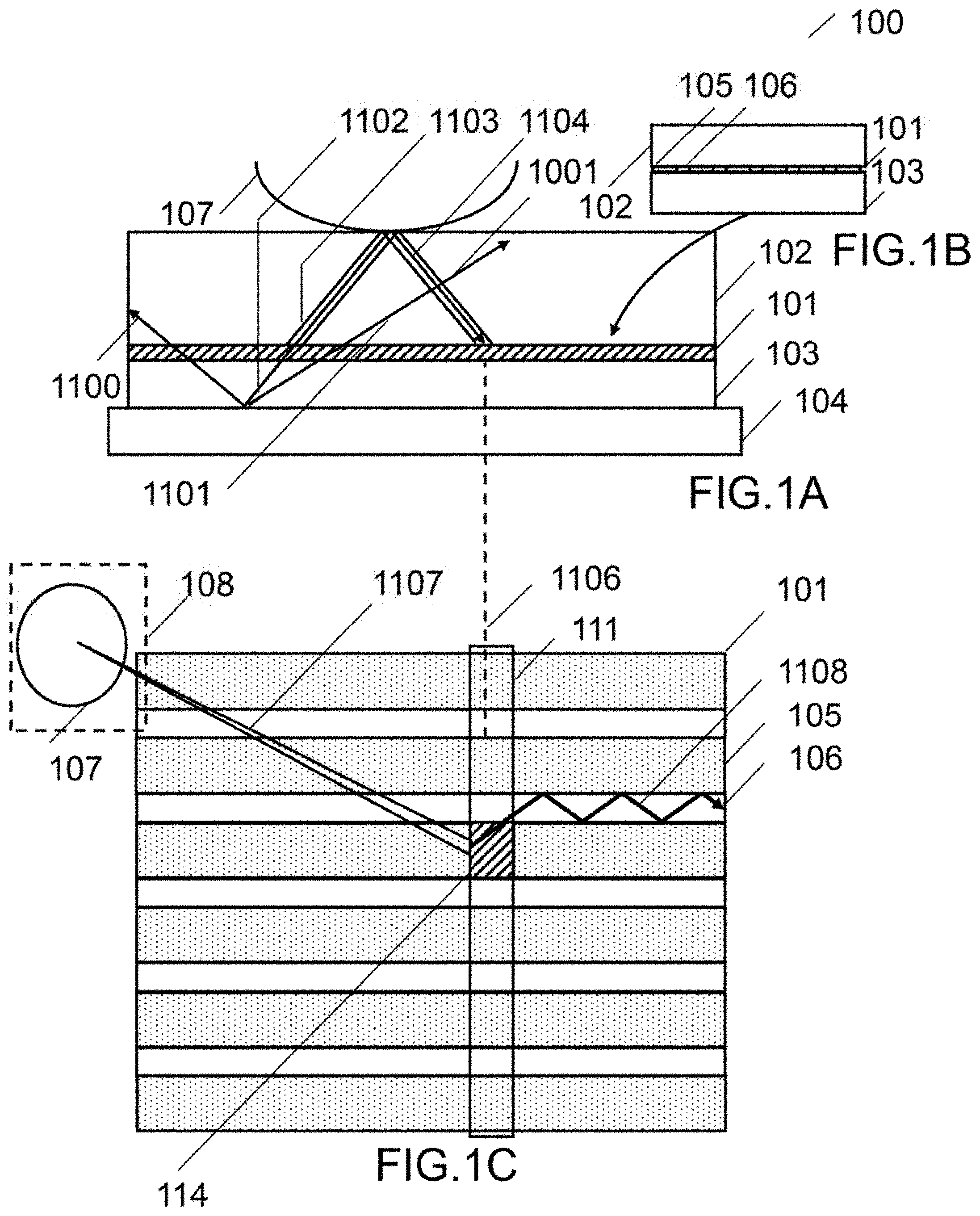
[0011] In one embodiment the diffracting state exists when an electric field is applied across the SBG element and the non-diffracting state exists when no electric field is applied.
[0012] In one embodiment when contact is made with an external material at a region on the platen a portion of the light incident at the region on the platen contacted by the external material is transmitted out of the platen, wherein light incident on the outer surface of the platen in the absence of the contact with an external material is reflected downwards.
[0013] In one embodiment when contact is made with an external material at a region on the platen a portion of the light incident at the region on the platen contacted by the external material is reflected downwards. Light incident on the outer surface of the platen in the absence of the contact with an external material is transmitted out of the platen.
[0014] In one embodiment the output from the detector is read out in synchronism with the switching of the electrode elements.
[0015] In one embodiment the light source is one of a laser or LED and the light is coupled into the waveguiding structure by one of a grating or a prism.
[0016] In one embodiment the switchable grating clad is a switchable Bragg grating recorded in one of a HPDLC grating, uniform modulation grating or reverse mode HPDLC grating.
[0017] In one embodiment the switchable grating clad includes at least one of a fold grating or a multiplexed grating or a rolled k-vector grating.
[0018] In one embodiment a method of making a contact image measurement comprising the steps of: [0019] a) Providing a waveguiding structure for propagating light in a first direction comprising, in series disposed in a layer sandwiched by transparent substrates, a first clad medium, a first core, a switchable grating clad, a second core, and a second clad medium; electrodes applied to opposing surfaces of the substrates at least one patterned into a set of parallel elements orthogonally traversing the cores; a light source optically coupled to the first and second cores; a platen in optical contact with the waveguiding structure; a detector optically coupled to the first and second core regions; [0020] b) coupling the light into a TIR path in the waveguiding structure; [0021] c) an external material contacting a region on the external surface of the platen; [0022] d) setting first and second electrode elements to a first voltage state and all other voltage-addressed electrodes set to a second voltage state; [0023] e) switchable grating regions overlapped by a first electrode element diffracting TIR light from first core into a path to the platen outer surface; [0024] f) switchable grating regions overlapped by a second electrode element diffracting light reflected from one of the region or the platen external surface into a TIR path in the second core; and [0025] g) transmitting the reflected light to the detector.
[0026] In one embodiment the first voltage state corresponds to a voltage being applied and the second voltage state corresponds to no voltage being applied.
[0027] In one embodiment the first voltage state corresponds to no voltage being applied and the second voltage state corresponds to a voltage being applied.
[0028] In one embodiment at least a portion of the light incident at the region on the platen is transmitted out of the platen, wherein at least a portion of the second optical path light not incident at the region is reflected.
[0029] In one embodiment at least a portion of the light incident at the region on the platen is reflected, wherein at least a portion of the second optical path light not incident at the region being transmitted out of the platen.
[0030] In one embodiment the waveguiding structure comprises a multiplicity of the cores and the dads cyclically arranged.
[0031] In one embodiment the voltages are applied sequentially, two electrodes at a time, to all electrodes in the array.
[0032] In one embodiment the output from detector is read out in synchronism with the switching of the electrode elements.
[0033] In one embodiment the contact image sensor is configured as a finger print scanner or a touch sensor.
[0034] A more complete understanding of the invention can be obtained by considering the following detailed description in conjunction with the accompanying drawings wherein like index numerals indicate like parts. For purposes of clarity, details relating to technical material that is known in the technical fields related to the invention have not been described in detail.
BRIEF DESCRIPTION OF THE DRAWINGS
[0035] FIG. 1A is a schematic side elevation view of a contact image sensor using a tablet computer as a light source in one embodiment.
[0036] FIG. 1B is a detail of schematic side elevation view of a contact image sensor using a tablet computer as a light source in one embodiment.
[0037] FIG. 1C is schematic plan view of a contact image sensor using a tablet computer as a light source in one embodiment.
[0038] FIG. 2A is a plan view of a transparent electrode array in one embodiment.
[0039] FIG. 2B is a scan line displayed on a computer tablet used as an illumination source in one embodiment.
[0040] FIG. 3 is a plan view of a fold grating in one embodiment
[0041] FIG. 4 is schematic side elevation view of a contact image sensor using a bidirectional waveguide in one embodiment.
[0042] FIG. 5 is schematic side elevation view of a contact image sensor using a bidirectional waveguide in one embodiment.
[0043] FIG. 6 is schematic plan view of a waveguide containing a fold grating used in a contact image sensor in one embodiment.
[0044] FIG. 7A is a schematic drawing of a waveguide structure used in contact image sensor in one embodiment.
[0045] FIG. 7B is a detail of a waveguide structure used in contact image sensor using a unidirectional illumination and detection waveguide in one embodiment.
[0046] FIG. 8A is a schematic side elevation view of a contact image sensor using a unidirectional illumination and detection waveguide in one embodiment.
[0047] FIG. 8B is a schematic plan view of a contact image sensor using a unidirectional illumination and detection waveguide in one embodiment.
[0048] FIG. 9 is a schematic plan view of a detail of contact image sensor using a unidirectional illumination and detection waveguide in one embodiment.
[0049] FIG. 10A is a cross section view showing ray propagation in a waveguide core in one embodiment
[0050] FIG. 10B is three dimensional view showing ray propagation in a waveguide core in one embodiment
[0051] FIG. 11A is a schematic plan view of a contact image sensor using a unidirectional illumination and detection waveguide in one embodiment.
[0052] FIG. 11B is a schematic cross section view of a contact image sensor using a unidirectional illumination and detection waveguide in one embodiment.
[0053] FIG. 12A is a schematic cross section view showing a stage in the process of fabricating a unidirectional illumination and detection waveguide in one embodiment.
[0054] FIG. 12B is a schematic cross section view showing a stage in the process of fabricating a unidirectional illumination and detection waveguide in one embodiment.
[0055] FIG. 12C is a schematic cross section view showing a stage in the process of fabricating a unidirectional illumination and detection waveguide in one embodiment.
[0056] FIG. 12D is a schematic plan view of an electrode structure in one embodiment
[0057] FIG. 13 is a schematic plan view of a waveguide structure for a unidirectional illumination and detection waveguide in one embodiment.
[0058] FIG. 14 is a schematic plan view of an electrode array coated substrate for a unidirectional illumination and detection waveguide in one embodiment.
[0059] FIG. 15 is a schematic plan view of a waveguide structure for a unidirectional illumination and detection waveguide in one embodiment.
[0060] FIG. 16 is a flow chart for making a contact image measurement using a unidirectional illumination and detection waveguide in one embodiment.
[0061] FIG. 17 is a schematic cross section view of a contact image sensor using a bidirectional waveguide and a multiplexed grating beam control layer in one embodiment.
[0062] FIG. 18 is a schematic plan view of a detail of the embodiment of FIG. 17.
[0063] FIG. 19 is a detail of a multiplexed grating beam control layer used in the embodiment of FIG. 17.
[0064] FIG. 20 is a grating characteristic of the embodiment of FIG. 0.17.
DETAILED DESCRIPTION OF THE INVENTION
[0065] It will be apparent to those skilled in the art that the present invention may be practiced with some or all of the present invention as disclosed in the following description. For the purposes of explaining the invention well-known features of optical technology known to those skilled in the art of optical design and visual displays have been omitted or simplified in order not to obscure the basic principles of the invention. Unless otherwise stated the term "on-axis" in relation to a ray or a beam direction refers to propagation parallel to an axis normal to the surfaces of the optical components described in relation to the invention. In the following description the terms light, ray, beam and direction may be used interchangeably and in association with each other to indicate the direction of propagation of light energy along rectilinear trajectories. Parts of the following description will be presented using terminology commonly employed by those skilled in the art of optical design. It should also be noted that in the following description of the invention repeated usage of the phrase "in one embodiment" does not necessarily refer to the same embodiment.
[0066] In the following description SBG (Switchable Bragg Grating) will refer to a Bragg grating that can be electrically switched between an active or diffracting state and an inactive or non-diffractive state. In the embodiments to be described below the preferred switchable grating will be a Switchable Bragg Grating (SBG) recording in a Holographic Polymer Dispersed Liquid Crystal (HPDLC) material. The principles of SBGs will be described in more detail below. For the purposes of the invention a non switchable grating may be one based on any material or process currently used for fabricating Bragg gratings. For example the grating may be recorded in a holographic photopolymer material. In some embodiments a non switchable grating may be provided by a surface relief grating.
[0067] An (SBG) is formed by recording a volume phase grating, or hologram, in a polymer dispersed liquid crystal (PDLC) mixture. Typically, SBG devices are fabricated by first placing a thin film of a mixture of photopolymerizable monomers and liquid crystal material between parallel glass plates. Techniques for making and filling glass cells are well known in the liquid crystal display industry. One or both glass plates support electrodes, typically transparent indium tin oxide films, for applying an electric field across the PDLC layer. A volume phase grating is then recorded by illuminating the liquid material with two mutually coherent laser beams, which interfere to form the desired grating structure. During the recording process, the monomers polymerize and the HPDLC mixture undergoes a phase separation, creating regions densely populated by liquid crystal micro-droplets, interspersed with regions of clear polymer. The alternating liquid crystal-rich and liquid crystal-depleted regions form the fringe planes of the grating. The resulting volume phase grating can exhibit very high diffraction efficiency, which may be controlled by the magnitude of the electric field applied across the PDLC layer. When an electric field is applied to the hologram via transparent electrodes, the natural orientation of the LC droplets is changed causing the refractive index modulation of the fringes to reduce and the hologram diffraction efficiency to drop to very low levels resulting in for a "non diffracting" state. Note that the diffraction efficiency of the device can be adjusted, by means of the applied voltage, over a continuous range from near 100% efficiency with no voltage applied to essentially zero efficiency with a sufficiently high voltage applied. U.S. Pat. Nos. 5,942,157 and 5,751,452 describe monomer and liquid crystal material combinations suitable for fabricating SBG devices.
[0068] To simplify the description of the invention the electrodes and the circuits and drive electronics required to perform switching of the SBG elements are not illustrated in the Figures. Methods for fabricated patterned electrodes suitable for use in the present invention are disclosed in PCT US2006/043938. Other methods for fabricating electrodes and schemes for switching SBG devices are to be found in the literature. The present invention does not rely on any particular method for fabricating transparent switching electrodes or any particular scheme for switching arrays of SBGs. Although the description makes reference to SBG arrays the invention may be applied using any type of switchable grating. To clarify certain geometrical of aspects of the invention reference will be made to A Cartesian (XYZ)coordinate system where appropriate.
[0069] In one embodiment illustrated in FIGS. 1-3 there is provided a contact image sensor in which line scanned illumination is provided by a computer tablet screen. The apparatus further comprises a platen 102, a waveguide layer 101 and a lower substrate 103 in contact with the screen of the table 104. The platen and lower substrate together provide a waveguide cell. Note that in practice it will be advantageous for the waveguide to be fabricated in a separate cell which is then laminated to the platen. As shown in the cross section detail of FIG. 1B and the plan view of FIG. 1C. The waveguide layer comprises alternating of strips of switchable SBG cladding 105 and polymer cores 106. Electrodes are applied to opposing faces of the platen and lower substrate. As shown in FIG. 2A at least one electrode 109 is patterned into column-shaped elements 109 disposed in an orthogonal direction to the waveguide cores. The electrodes are used to switch portions of the clad between non-diffracting states. A clad region in its diffracting states couples light reflected from the platen surface into an adjacent core. All core regions under an addressed electrode are switched simultaneously. FIG. 1C shows one such grating region indicated by 114 lying under the voltage addressed electrode 109. This grating region diffracts the reflected light 1107 into the TIR light path 1108. As will be discussed later the diffracting state may occur with or without an applied voltage across the grating according to the type of holographic material system used. Note that the light has been illustrated as undergoing TIR in the plane of the drawing. However, in practice, the grating orientation (as defined by the grating k-vector) and reflected beam vector will result in a more complicated TIR path which will typically result in rays undergoing a spiral TIR path down each core. The signals from the waveguide cores are collected by a linear detector at the end of the waveguide. In the simplest embodiment each waveguide core abuts a pixel of the detector. However, other coupling schemes should be apparent to those skilled in ther art. At any time the tablet 112 displays a column 115 of width a few pixels against a black background 116 as illustrated in FIG. 2B. The bright column is scrolled continuously across the tablet screen. The width of the column may be just one pixel. In practice a width of several pixels may be required to achieve an adequate signal level. The tablet based on LCoS or LED technology will normally emit light over a large cone angle as indicated by ther rays 1100,1101. A small portion of this light lying within a small solid angle will be totally internally reflected at the outer surface of the platen as indicated by the rays 1103-1104. The reflected light 1104 is then coupled into a waveguide by an active region of the waveguide as discussed above. In one embodiment wherever an external body such as a finger touches the platen, it "frustrates" the reflection process, causing light to leak out of the platen. Thus, the parts of the skin that touch the platen surface reflect very little light, forming dark pixels in the image. The image is built up line by line into a finger print image. A key advantage of this embodiment is that the tablet eliminates the need for a separate scanner layer allow making the sensor thinner, cheaper and lower power consumption. However, the use of visible light may preclude its application in many security applications.
[0070] The complex beam steering required to couple the light reflected from the platen in the waveguide cores requires a grating structure referred to by the inventors as a fold grating. This type of grating is normally used for changing beam direction and providing beam expansion within a waveguide. Gratings designed for coupling light into or out of a waveguides are tilted around an axis lying in the waveguide plane. Fold gratings have a more generalized tilt. In their simplest implementation, as used in the present invention, they are tilted around an axis perpendicular to the waveguide plane such they deflect beams in the waveguide plane. More generally, they may have tilts defined by two rotation angles so that, for example, light can be coupled into the waveguide and deflected into an orthogonal direction inside the waveguide, all in one step. FIG. 3 is a plan view of a basic fold grating 118. When the set of rays 1110 encounter the grating, they diffract in a manner that changes the direction of propagation by 90.degree.. Note that when a ray encounters the grating, regardless of whether it intersects the grating from above or below, a fraction of it changes direction and the remainder continues unimpeded. A typical ray will interact many times with vertically (in the Y direction) while some light will be moving laterally (in the X direction). From a design perspective, it is desirable to engineer the amount of light 1111 emerging from the output edge of the grating to be uniformly distributed laterally and the amount of light 1112 emerging from the side edge of the grating to be as small as possible.
[0071] In one embodiment illustrated in FIG. 4 an illumination layer sensor for providing line scanned illumination and a detector layer from receiving reflected light from a platen and transmitting it to an infrared detector are combined in a single SBG array waveguide layer. The contact image sensor comprises a waveguide grating layer 161 a transmission grating 162 a platen 163, a light source 165 and a detector 166. In one embodiment the transmission grating and waveguide are air separated. In one embedment the transmission grating and waveguide are separated by a think layer of low index nanoporous material. Light from the source is coupled into a TIR path 1140 in the waveguide by a coupling grating 167. The waveguide contains an array of switchable grating elements such as 164 which is shown in its diffracting state. The grating elements switch in scrolling fashion, each element in its diffracting state diffracting light output out of the waveguide toward the transmission grating. For example the active element 164 diffracts the TIR light into the direction 1141, typically normal to the waveguide. The transmission grating deflects the light into the direction 1142 inside the platen meeting the platen surface TIR conditions. Light reflected from the platen 1143 passes through the transmissive grating without deviation since it is now off-Bragg (that is, it lies outside the diffraction efficiency angular bandwidth of the grating as predicted by Kogelnik theory). The optical surfaces of the waveguide are roughened to ensure that at least a small portion of the reflected light from the platen enters the TIR path 1144 to the detector. Advantageously, the source and detector operate in the infrared. The detector is typically a linear detector.
[0072] In one embodiment illustrated in the cross sectional view of FIG. 5 a contact image sensor similar in concept to the one of FIG. 4 comprises a waveguide 170, a first passive transmission Bragg grating 171 a second passive transmission Bragg grating 174, and a platen 175. The waveguide contains a SBG grating array 176 comprising column shaped elements, an input coupling grating 177 for coupling light from an infrared source 178 into the waveguide. The apparatus further comprises a light output coupling grating 180 for directing light onto a linear infrared detector array 181. The transmission Bragg gratings may be recorded in a holographic photopolymer or in a HPDLC material, the latter providing an attractive passive medium owing to its high index modulation capability. At any time two elements of the grating array, such as the ones indicated by 176A,176B are in a diffracting state. We next consider the light path through the contact image sensor. Light 1150 from the source is coupled into a TIR path 1151 in the waveguide by the input grating. The active grating element 176B deflects the light out of the waveguide into the direction 1152 which is typically normal to the waveguide. The second passive grating 173 diffracts the light into the platen in the direction 1153. After reflection from the platen outer surface the light 1154 is diffracted toward the waveguide by the first passive grating 171 in the direction 1155 which is substantially normal to the waveguide. The light is coupled into the TIR path 1156 by the active grating element 176A and is finally deflected out of the waveguide by the output coupling grating onto the infrared detector. In one embodiment the apparatus of FIG. 5 further comprises polarization components such as half wave plates and quarter wave plates for controlling beam polarization to achieve more efficient bidirectional transmission of light within the waveguide as disclosed in PCT Application No.: PCT/GB2014/000295 entitled METHOD AND APPARATUS FOR CONTACT IMAGE SENSING
[0073] In one embodiment illustrated in FIG. 6 a contact image sensor waveguide comprises an array of switching SBG columns 182 and fold grating 183. Signal light 1160, 1161 from the SBG array is deflected into an orthogonal direction by the fold grating and transmits light towards the linear detector array 184. The advantage of this scheme is the output beam can be tailored to match the length of standard linear arrays. This allows more flexibility in the specification of the platen area and aspect ratio.
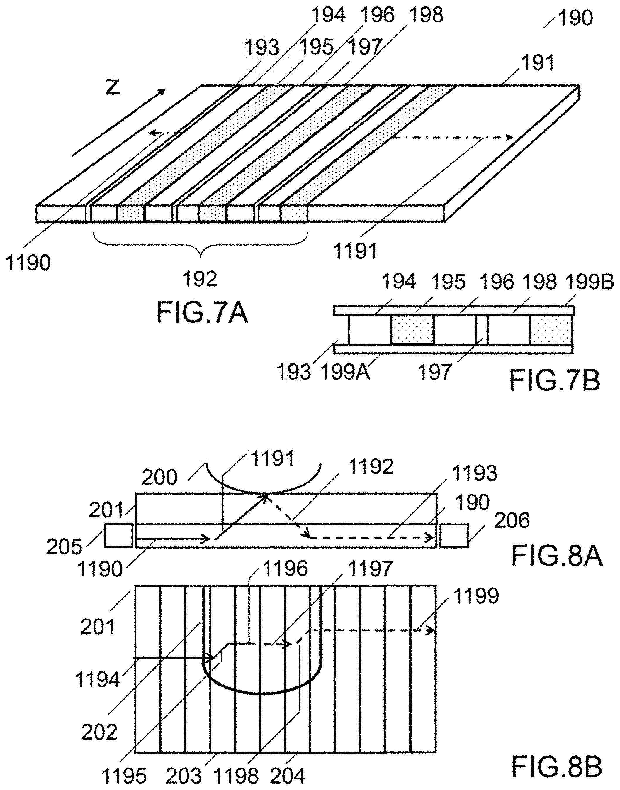
[0074] In one embodiment illustrated in FIGS. 7-15 there is provided a contact image sensor in which the receiver and transmit functions are combined in a single unidirectional waveguide. Unidirectional here means that the illumination and the reflected light from the platen propagated in the same direction (but not in the same waveguide core). Referring to the FIG. 7A and FIG. 7B, the waveguide 190 comprises a layer 191 containing a cyclically repeated waveguiding structure 192 for propagating light in a first direction comprising, a first clad medium 193, a first core 194, a switchable grating clad 195, a second core 196, and a second clad medium 197. The light propagation direction z is indicated. The first clad medium 193 and second clad medium 197 have a low refractive index to ensure that there is no cross talk between adjacent waveguide cores. Ideally, the first clad and second clad media are air or a low index nanoporous material (ideally with a refractive index well below 1.3). The switchable grating clad contains a fold grating with a k-vector orientated in 3D space. The waveguide layer is sandwiched by transparent substrates 1991A, 199B. In one embodiment of the substrates provides a platen. However, advantageously, the waveguide would be fabricated in a separate cell which is then laminated to the platen. Transparent electrodes are applied to opposing surfaces of the substrates at least one being patterned into a set of parallel elements orthogonally traversing the cores. An infrared source is optically coupled to the first and second cores. Finally a detector is optically coupled to the first and second core regions. The dashed lines 1190, 1191 in FIG. 7A indicate the continuation of the waveguide core and clad elements. For the sake of simplicity we shall consider the minimum configuration ie first and seconds cores a switchable grating clad and first and second clad media as discussed above. The switching electrodes have very small gaps. In one embodiment, the basic core clad group 192 has a total width of 50.8 um to provide a 500 dpi repeat pattern. In one embodiment the voltages are applied sequentially, two electrodes at a time, to all electrodes in the array. The output from the detector is read out in synchronism with the switching of the electrode elements. The first core provides an illumination (or transmitter) waveguide while the second core provides a signal (or receiver) waveguide. The SBG clad essentially `opens` a side of the waveguide wall, allowing light to bounce up onto the platen, onto the finger, and back down onto the SBG fold, but significantly further up the waveguide (by an amount determined by the platen thickness). In the embodiment illustrated the electrodes are orthogonal to the cores and clad. In one embodiment the electrodes are tilted at a small angle to the normal to the waveguide direction (in the plane of the waveguide) to overcome the risk of cross coupling between neighboring cores. In one embodiment the SBG clad is in direct contact with the platen layer. In other embodiments the SBG clad may be separated from the platen layer by intermediate transparent layers. In some embodiments it may be advantageous to have LC alignment layers in proximity to the SBG clad to promote more optimal alignment of the LC directors in the SBG clad. In some embodiments polarization control layers may be provided in proximity to the waveguide layer.
[0075] The operation of the contact image sensor will now be discussed in more detail. FIG. 8A shows a schematic cross section of the platen 200 and waveguide 190. FIG. 8B is a plan view showing the electrode array 201 and finger 202 in contact with the platen. First and second simultaneously voltage-addressed electrodes are indicated by 203,204. The light propagation direction z is indicated by an arrow. Considering the cross section view of FIG. 8A, light incident in one waveguide cores is indicated by 1190. This light is diffracted upwards towards the platen by a SBG clad region overlaid by the first voltage addressed electrode. The reflected light 1192 is diffracted into a second core by the SBG clad region overlaid by the second voltage-address electrode. FIG. 8B shows the sideways displacement of the guided light. The input path in the first waveguide is deflected sideways and up to the platen by the SBG clad region overlaid by the first voltage-addressed electrtode 203 as indicated by the rays 1195,1196. On reflection the downward light 1197 undergoes a further sideways shift when it interacts with the SBG clad region overlaid by the second voltage-addressed electrode 204 as indicated by the rays 1197,1198. Finally the light proceeds along a TIR path along the second waveguide core up to the detector.
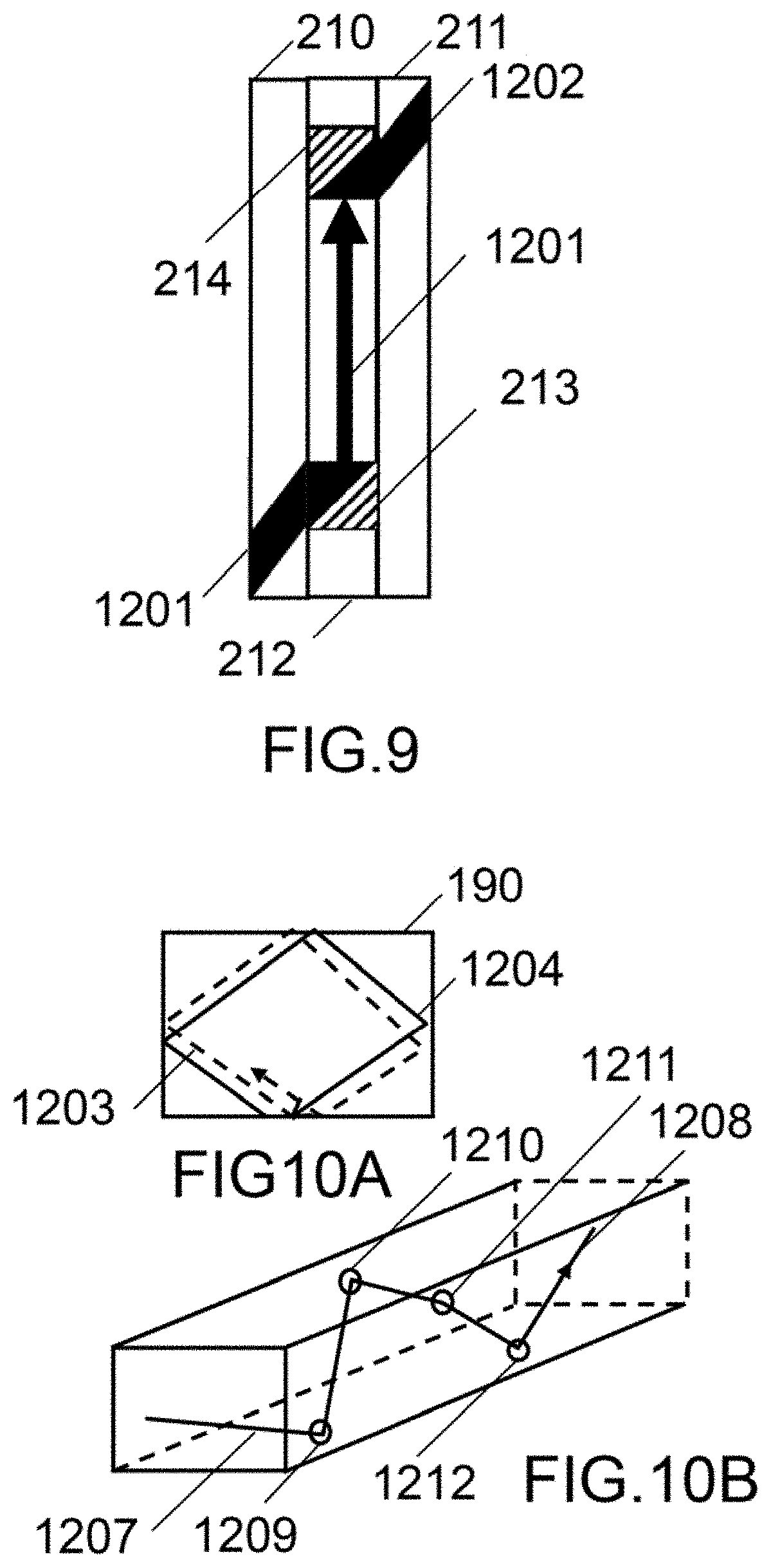
[0076] The coupling of light between two cores via the SBG clad region is illustrated in plan view in FIG. 9 which shows first and second cores 210,211 separated by the SBG clad 212. Two regions of the SBG clad simultaneously addressed by first and second electrodes (not shown) are indicated by shaded areas 213,214. The wave guided beam 1201 (from the infrared source) in the first core is coupled by the SBG grating region overlapped by the first voltage-addressed electrode into a path up to the platen. At the platen the beam undergoes total internal reflection and propagates into the SBG region overlapped by the second voltage-addressed electrode. Here it is diffracted into the TIR path 1202 in the second core (leading to the detector)
[0077] Examples of the TIR paths in the cores are illustrated in the core cross section view of FIG. 10A and the three dimensional view of a portion of a core in FIG. 10B. The grating orientation (as defined by the grating k-vector) and the reflected beam vector results in the spiral TIR path indicated by the ray paths 1203,1204 in FIG. 10A and the ray paths 1207,1208 shown interacting with the reflected faces of the core at points 1209-1212 in FIG. 10B.
[0078] FIG. 11A is a plan view of the waveguide showing the propagation of illumination and signal light between neighboring waveguide cores. The section of the waveguide array illustrated comprises a first clad region 222, a first core 223, a SBG clad 224, a second core 225, a second clad region 226. Transparent electrodes 227-230 traverse the cores and dads. The illumination light in first core follows TIR path 1220-1222. Electrodes 227,230 are simultaneously voltage addressed such that SBG regions 231,232 are switched into their diffracting states. The TIR ray 1120 is coupled into the first core is diffracted upwards towards the platen as indicated by the rays 1222, 1223. After reflection at the outer surface of the platen the reflected ray 1224 is diffracted by the SBG region 231 as indicated by the rays 1225 and coupled into a TIR path 1226 within the second core 225 which transmits the signal light to an element of the linear infrared detector (not shown). FIG. 11B is a cross section of the waveguide in the YZ plane showing a projection of the ray paths in the first core, SBG clad and second core. FIG. 11B uses the labelling of FIG. 11A. The TIR path in the first core is indicated by the rays 1230, the coupling of the TIR light and diffraction up to the platen is represented by the ray 1234; the reflection of the light from the platen and coupling into the second core is represented by 1235; and the TIR path in the second core is represented by 1236.
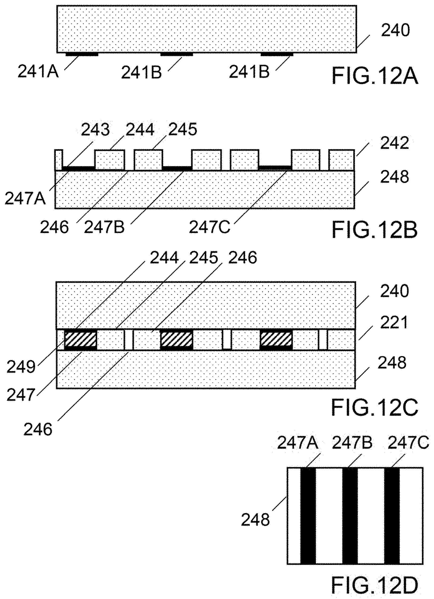
[0079] FIG. 12 illustrates three stages in the fabrication of the waveguiding structures. In a first stage illustrated in FIG. 12A patterned electrodes are applied to a transparent substrate. In a second stage shown in FIG. 12B a lower substrate is etched to form cavities for the clad material and electrodes coatings are applied to the bases of the cavities to be filled with SBG recording material. In a next key stage of the process the SBG clad cavities are filled with holographic material and exposed to form fold gratings. After curing of the hologram the upper and lower substrates are laminated as shown in FIG. 12C. The electrode pattern used for at least one of the coatings applied to the substrates in FIG. 12A or FIG. 12B is shown in FIG. 12D. Either the upper or lower substrate electrodes may be patterned in this way with the opposing substrate surface having a continuous electrode coating. In one embodiment both electrodes are patterned according to FIG. 12D. The processes for etching substrates and applying patterned electrodes are well known to those skilled in the art. Other intervening steps will be required for coating etching holographic recording and gluing and illuminination, as should be apparent to those skilled in the art. Examples of a waveguide plate and a patterned electrode plate based on the principles of FIG. 12 are shown in FIGS. 13-14.
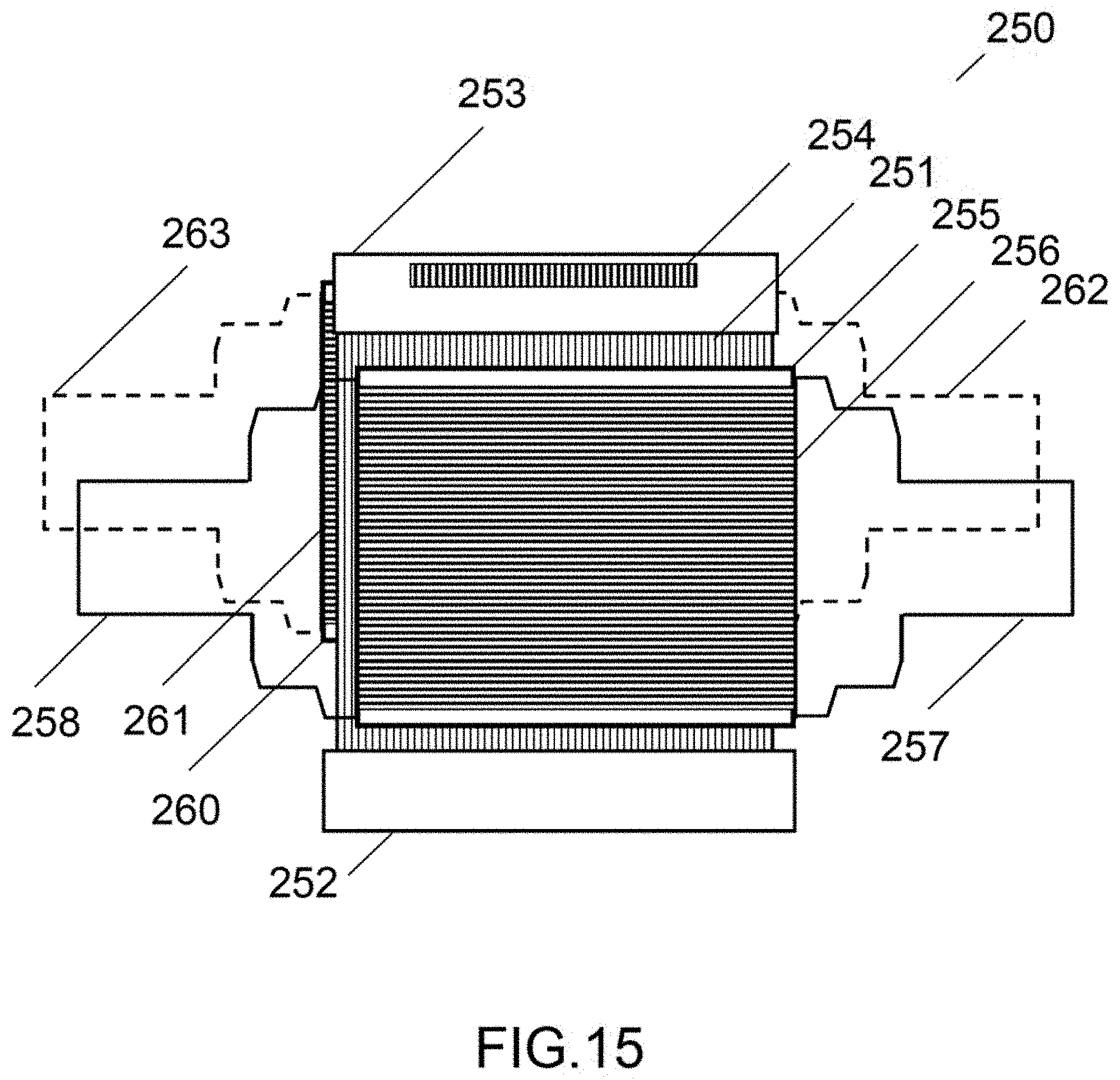
[0080] FIG. 15 shows elements of the waveguide structure 250 in one embodiment comprising a waveguide array layer 251, an infrared source module, beam expansion and waveguide coupling optics 252, an infrared detector module 253, comprising a linear infrared detector array 254. The apparatus further comprises a first substrate with patterned electrode coating 256, flexible electrical connectors 257,258 linking the electrodes to a drive module and power supply (not shown), and a second substrate 260 with patterned electrode coating 261, with flexible electrical connectors 262,263 linking the electrodes to the drive module and power supply. Note that one of the substrates may comprise the waveguide substrate described in FIG. 12.
[0081] In one embodiment the diffracting state of the SBG clad exists when no electric field is applied across the SBG element and the non-diffracting state exists when an electric field is applied. In one embodiment the diffracting state exists when an electric field is applied across the SBG element and the non-diffracting state exists when no electric field is applied. Materials having this property are referred to as reverse mode.
[0082] In one embodiment the SBG clad is recorded in a reverse mode HPDLC material. Reverse mode HPDLC differs from conventional HPDLC in that the grating is passive when no electric field is applied and becomes diffractive in the presence of an electric field. The reverse mode HPDLC may be based on any of the recipes and processes disclosed in PCT Application No.: PCT/GB2012/000680, entitled IMPROVEMENTS TO HOLOGRAPHIC POLYMER DISPERSED LIQUID CRYSTAL MATERIALS AND DEVICES.
[0083] In one embodiment when contact is made with an external material at a region on the platen a portion of the light incident at the region on the platen contacted by the external material is transmitted out of the platen. Light incident on the outer surface of the platen in the absence of the contact with an external material is reflected downwards. In one embodiment when contact is made with an external material at a region on the platen a portion of the light incident at the region on the platen contacted by the external material is reflected downwards. Light incident on the outer surface of the platen in the absence of the contact with an external material. is transmitted out of the platen.
[0084] The light source in any of the embodiments may be a laser or LED desirably operating in the infrared. Light is coupled into the waveguiding structure by one of a grating or a prism. In one embodiment the coupling grating or prism is clocked. In the case of a grating this means that the projection of the k-vector in the plane of the waveguide layer is an angle to the waveguide long axis. Clocking the input coupler will normally result in a spiralling of the TIR path within the waveguide. In combination with the fold grating in the SBG layer this property can be used to control the grating coupling efficiency and angular response.
[0085] In one embodiment the SBG clad is recorded in a uniform modulation holographic material system. Exemplary uniform modulation liquid crystal-polymer material systems are disclosed in United State Patent Application Publication No.: US2007/0019152 by Caputo et al and PCT Application No.: PCT/EP2005/006950 by Stumpe et al. both of which are incorporated herein by reference in their entireties. Uniform modulation gratings are characterized by high refractive index modulation (and hence high diffraction efficiency) and low scatter.
[0086] In one embodiment the SBG clad includes at least one of a fold grating or a multiplexed grating or a rolled k-vector grating. Multiplexed gratings and rolled k-vectors may be used to improve the angular response of the SBG clad. The application of multiplexing, and spatial varying thickness, k-vector directions and diffraction efficiency in the present invention may be based on the embodiments, drawings and teachings provided in U.S. patent application Ser. No. 13/506,389 entitled COMPACT EDGE ILLUMINATED DIFFRACTIVE DISPLAY, U.S. Pat. No. 8,233,204 entitled OPTICAL DISPLAYS, PCT Application No.: US2006/043938, entitled METHOD AND APPARATUS FOR PROVIDING A TRANSPARENT DISPLAY, PCT Application No.: GB2012/000677 entitled WEARABLE DATA DISPLAY, U.S. patent application Ser. No. 13/317,468 entitled COMPACT EDGE ILLUMINATED EYEGLASS DISPLAY, U.S. patent application Ser. No. 13/869,866 entitled HOLOGRAPHIC WIDE ANGLE DISPLAY, and U.S. patent application Ser. No. 13/844,456 entitled TRANSPARENT WAVEGUIDE DISPLAY.
[0087] In one embodiment there is provided a method of making a contact image measurement comprising the steps of: [0088] a) providing a waveguiding structure for propagating light in a first direction comprising, in series disposed in a layer sandwiched by transparent substrates, a first clad medium, a first core, a switchable grating clad, a second core, and a second clad medium; electrodes applied to opposing surfaces of the substrates at least one patterned into a set of parallel elements orthogonally traversing the cores; a light source optically coupled to the first and second cores; a platen in optical contact with the waveguiding structure; a detector optically coupled to the first and second core regions; [0089] b) coupling the light into a TIR path in the waveguiding structure; [0090] c) an external material contacting a region on the external surface of the platen; [0091] d) setting first and second electrode elements to a first voltage state and all other voltage-addressed electrodes set to a second voltage state; [0092] e) switchable grating regions overlapped by a first electrode element diffracting TIR light from first core into a path to the platen outer surface; [0093] f) switchable grating regions overlapped by a second electrode element diffracting light reflected from one of the region or the platen external surface into a TIR path in the second core; and [0094] g) transmitting the reflected light to the detector.
[0095] In one embodiment the first voltage state corresponds to a voltage being applied and the second voltage state corresponds to no voltage being applied. In one embodiment the first voltage state corresponds to no voltage being applied and the second voltage state corresponds to a voltage being applied. This applies to reverse mode materials.
[0096] In one embodiment at least a portion of the light incident at the region on the platen is transmitted out of the platen, wherein at least a portion of the second optical path light not incident at the region is reflected. In one embodiment at least a portion of the light incident at the region on the platen is reflected, wherein at least a portion of the second optical path light not incident at the region being transmitted out of the platen.
[0097] In one embodiment the waveguiding structure comprises a multiplicity of the cores and the dads cyclically arranged.
[0098] In one embodiment the voltages are applied sequentially, two electrodes at a time, to all electrodes in the array.
[0099] In one embodiment the output from detector is read out in synchronism with the switching of the electrode elements.
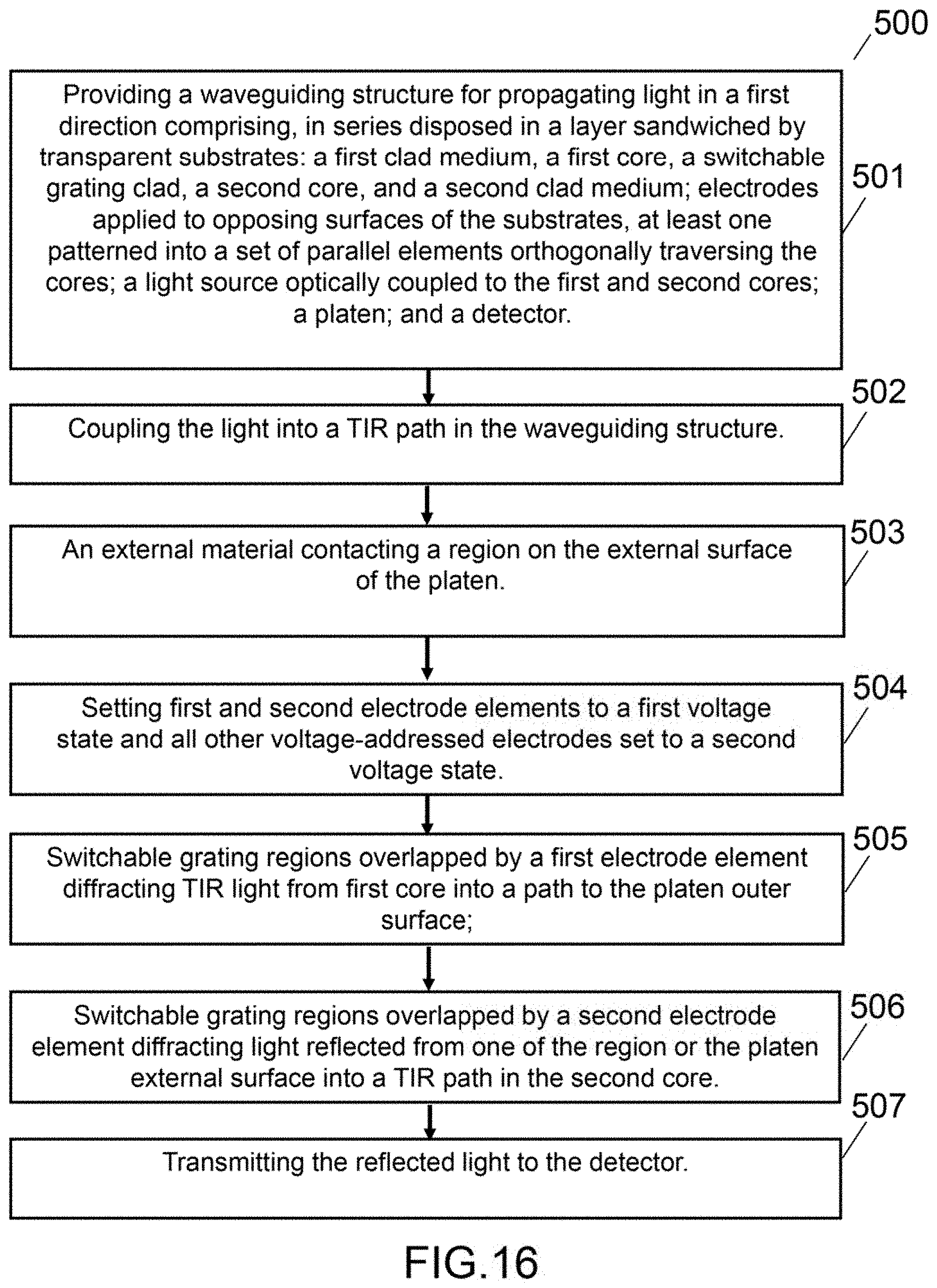
[0100] A method of a method of making a contact image measurement in one embodiment of the invention in accordance with the basic principles of the invention is shown in the flow diagram in FIG. 14. Referring to the flow diagram 500, we see that the said method comprises the following steps. [0101] At step 501 providing a waveguiding structure for propagating light in a first direction comprising, in series disposed in a layer sandwiched by transparent substrates, a first clad medium, a first core, a switchable grating clad, a second core, and a second clad medium; electrodes applied to opposing surfaces of the substrates at least one patterned into a set of parallel elements orthogonally traversing the cores; a light source optically coupled to the first and second cores; a platen in optical contact with the waveguiding structure; a detector optically coupled to the first and second core regions; [0102] At step 502 coupling the light into a TIR path in the waveguiding structure; [0103] At step 503 an external material contacting a region on the external surface of the platen; at step 504 setting first and second electrode elements to a first voltage state and all other voltage-addressed electrodes set to a second voltage state; [0104] At step 505 switchable grating regions overlapped by a first electrode element diffracting TIR light from first core into a path to the platen outer surface; [0105] At step 506 switchable grating regions overlapped by a second electrode element diffracting light reflected from one of the region or the platen external surface into a TIR path in the second core; and [0106] At step 507 transmitting the reflected light to the detector.
[0107] In one embodiment shown in FIG. 17 a contact image sensor 300 comprises a platen 301 overlaying multiplexed Bragg grating layer 302 containing the multiplexed gratings 303,303 which have opposing slant angles and differing grating pitches, a bidirectional waveguide 305 contain switching bidirectional grating 306, input grating 307 an output put grating 309 grating elements 309 and 310 are shown in their diffracting states. The input and output gratings are passive gratings. The bidirectional waveguide is sandwich by the layers 311, 312 which are shown in more detail in FIG. 17. The input and output gratings are coupled to a laser source 313 and detector 314. Then input grating couples the light 1240 from the laser into the TIR path 1241. The active grating element 309 couples this light toward the multiplexed grating layer in the beam direction 1242. The multiplexed grating 303 layer diffracts a portion of the light into the direction 1243 and the grating 304 diffracts a portion of the light into the direction 1244. The first beam is directed to a light trap, which is not illustrated. The second beam is reflected at the outer platen surface a beam 1255 which interacts with the multiplexed grating a second time and is diffracted by the grating 304. This light is coupled into a TIR path in the bidirectional waveguide by the active element 310. Note that the separation of the addressed grating elements is determined by the reflection path. The in-coupled light follows the TIR path 1248 up the output grating and is diffracted in to the output beam 1249 toward the detector. The platen and passive transmission multiplexed grating are separated from the bidirectional waveguide by either an air gap or, ideally, a low index layer. In one embodiment the SBG array is comprised of 1600 column SBG elements each overlapped by 48.8 micron wide etched ITO electrodes on a glass substrate (the element pitch is 50.8 micron pitch equivalent to 500 elements/inch). In the waveguide, light from the backlight is trapped by total internal reflection, unless one of the column-shaped grating segments happens to be active.
[0108] When an active segment is encountered, a thin lamina of light is diffracted out of the waveguide. By rapidly switching the columns ON and OFF in sequence, a thin sheet of light can be engineered to sweep across the surface of the scanner and into the tilt grating. During a scan, the user's four fingers are placed onto the platen surface. Wherever the skin touches the platen, it "frustrates" the reflection process, causing light to leak out of the platen. Thus, the parts of the skin that touch the platen surface reflect very little light, forming dark pixels in the image. The image is built up line by line into a 500 dpi, FBI-approved industry standard picture. The second function of the bidirectional waveguide is to provide a waveguide path to propagate signal light from the platen to a detector array.
[0109] FIG. 18 shows a detail 320 of the bidirectional waveguide 305 of FIG. 17. The waveguide is sandwiched by the layers 312 and 313. Confinement of the reflected beams from the platen is achieved by applying thin stripes of infrared (IR) absorbing material 322 separated by clear regions 323 to the top substrate 312 and roughening or frost-etching the bottom substrate into striped regions 325 separated by clear regions 326 overlapping the IR absorbing regions. Note that the IR absorbing and frost-etched strips are typically much narrower than the adjacent transparent regions. The IR stripes define parallel propagation channels terminating at a high resolution infrared linear detector array. Collimated reflected beams from the platen enter the detector layer in the gaps between the IR absorbing stripes and undergo TIR within up to the detector array. Hence the beam propagation is analogous to that provided by waveguide cavities. Light scattered out of a give channel is scattered by the frosted layer and absorbed by the IR coating. Any forward scattered light or multiple scatter between near neighbouring channels will tend to diminish in intensity with each ray surface interaction and will form a background noise level that can be subtracted from the fingerprint signature by the processing software.
[0110] The key challenge in the embodiment of FIG. 17 is how to separate the upward-diffracted and platen-reflected beams (illumination and signal beams) in the bi-directional waveguide. If the signal beam follows a path parallel to that of the illumination beam it will end up being diffracted back towards the illuminator. This is a consequence of the symmetry of diffraction gratings. To overcome this problem we use two different grating prescriptions in the waveguide. This can be accomplished in a single grating layer with all the necessary grating functionality being encoded into the holographic master during fabrication. A first grating prescription provides the array used to scan the beam; TIR illumination light being diffracted vertically upwards. The second grating prescription, which is used in the portion of the SBG layer overlapping the illumination source (that is, the grating 307) is designed to have a narrow angular bandwidth. By narrow angular bandwidth we mean that the diffraction efficiency versus angle profile has a narrow FWHM (full width half maximum) width. If the signal beam is offset from the illumination beam by a small angle it will not re-interact with the upward-diffracting gratings but will be diffracted by the detector grating. This narrower angular bandwidth is achieved by making the grating thicker. The purpose of the multiplex gratings is to provide the required angular offset. One of the two multiplexed gratings is designed to tilt the illumination beam into the correct angle for TIR at the platen surface the second multiplexed gratings diffracts the light reflected off the platen, the signal beam, into a direction at a small angle (around 3-4 degrees) to the vertical. This light is rediffracted by the scanner grating which has a bandwidth large enough to diffract the light and has a grating vector biassed to a give a strong DE for the signal beam. (Typically, the required angular bandwidth is achieved by limiting the grating thickness to around 3 microns). The signal light proceeds to TIR along the waveguide until it is diffracted out of the waveguide towards an infrared detector array by the detector grating. Owing to the low angular bandwidth of the illumination input grating very little of the signal light will be diffracted towards the illumination backlight. Cross-coupling between the detector and illumination channels is thus avoided.
[0111] Cross coupling must also be addressed in the multiplex grating layer in the embodiment of FIG. 17. FIG. 19 shows a detail of the multiplexed grating layer (labelled 331 which is shown sandwiched between the platen 301 and a further transparent substrate 334. Note that for ease of fabrication a further transparent substrate can be disposed between the multiplexed grating layer and the platen so that the multiplexed grating components can be recorded in a separated cell that is laminated with the paten. FIG. 18 illustrates the basic ray optics showing the two multiplex gratings 332,333 also labelled by G1,G2 with grating vectors (normal to the grating fringes) K.sub.1,K.sub.2. The useful signal corresponds to the ray paths in which illumination light interacts first with G1 and then with G2 that is the ray path comprises the rays 1265-1268 emerging from the multiplexed grating layer at angle .theta. to the surface normal 1269. These reflections satisfy the Bragg condition and are therefore called on-Bragg (as opposed to ray-grating interactions such as those at points A, B which do not satisfy the Bragg condition and are called off-Bragg). The unwanted light (or noise signal) corresponds to a second set of paths in which the illumination light interacts first with G2 and then with G1 for example the rays 1260-1263 emerging from the multiplexed grating layer at angle .theta. to the surface normal 1264. From grating symmetry the first and second paths illustrated are reciprocal. The input beams for the signal and noise paths are each nominally at 0.degree. to the platen. Noise is suppressed by designing G1 and G2 to have slightly different slant angles and pitches (fringe spacings). The noise and signal beams are the same offset angles but are engineered to suppress the noise and maximize the signal. G2 weakly in-couples illumination light at 0.degree. but strongly out-couples the waveguide angle .theta.. On the other hand, G1 weakly out-couples light at angle .beta.-.delta..theta. to the platen normal (where .beta. is the total internal reflection angle at the platen for the ray path 1260-1263 and is a small angular increment). However the grating G1 strongly in-couples signal at waveguide angle. In one embodiment the grating G2 has construction angles 4.degree. and 47.degree. and grating G1 has construction angles 0.degree. and 47.degree.. In each case the wavelength is 785 nm, the average index of the hologram is 1.53, the hologram thickness is 15 micron and the holographic refractive index modulation is 0.002. One issue to be addressed is that the multiplexed grating causes a split platen interrogation signal (owing to diffracted and 0-order non-diffracted light being produced at each beam-grating interaction. This process will result in some light loss out of the platen. However, this signal loss can be mitigated by using a powerful laser and by making the multiplexed grating thicker. A further issue is that stray (0-order) light reflected vertically downwards from the platen could contribute to the noise level. This problem can be avoided by tilting the illumination beam diffracted from the bidirectional waveguide by up to say 10.degree.. Any directly reflected light would then be at 10.degree. relative to the SBG detector layer, and then would fall outside the angular bandwidth of the SBG, pass straight through and be dumped. Stray light reflected inside the platen and multiplexed grating layer can be trapped using prismatic elements (or other equivalent means.
[0112] The inventors are confident that they can fabricate high quality multiplexed gratings that deliver the above functionality. SBG Labs has already demonstrated multiplexed gratings in more challenging applications. In the present case the gratings are at opposing slant angles which is generally considered to be most favourable consideration for producing high diffraction efficiency and uniformity while avoiding the grating formation competition that can occur which gratings are slanted at similar directions. Our mastering and replication processes for multiplexed gratings are at any advance stage of development
[0113] The characteristics of a typical SBG grating for use in the in the bi-directional waveguide of FIG. 17 are illustrated in FIG. 20 which shows a plot 1280 of the diffraction efficiency versus angle 1281. The input angle is indicated by 1282 and the output angle by 1283. Normally, the SBG grating is designed to provide an input angle of 0.degree. with a FWHM angular bandwidth 1290 greater than 4.degree. (corresponding to the optimum multiplexed grating offset angle). This is will within the range of angular bandwidths that can be achieved with our gratings. The SBG angular bandwidth is broad enough to both output illumination light from the bi-directional waveguide, and re-couple signal light from the platen at the input angle plus the 4.degree. degree offset introduced by the multiplexed gratings. The SBG chief ray is offset by half of the multiplexed grating offset angle, that is, by 2.degree.. In one embodiment the grating has construction angles 2.degree. and 47.degree.; an operating wavelength of 785 nm. a hologram average refractive index of 1.53, a hologram thickness of 4 micron, a grating period of 670 nm. and an index modulation of 0.056. A grating thickness of 4-5 micron is found to switch effectively.
[0114] In any of the above embodiments, during a scan, the user's four fingers are placed onto the platen surface. Wherever the skin touches the platen, it "frustrates" the reflection process, causing light to leak out of the platen. Thus, the parts of the skin that touch the platen surface reflect very little light, forming dark pixels in the image. The image is built up line by line into a 500 dpi, FBI-approved industry standard picture. In the absence of finger contact the light incident on the platen outer surface is totally internally reflected downwards towards the wave guiding structure 50 and then on to the detector. The X coordinate of the contacting feature is given by the detector array element providing the dark-level or minimum output signal. The latter will be determined by the noise level of the detector. The Y coordinate of the contacting feature is computed from the geometry of the ray path from the last SBG element in the first SBG array that was in a diffracting state just prior to TIR occurring in the platen and a signal from the reflected light being recorded at the detector. In one embodiment of the invention an alternative detection scheme based on the principle that in the absence of any external pressure art the platen/air interface the incident light is transmitted out of the platen. Now, external pressure from a body of refractive index lower than the platen (which may a feature such as a finger print ridge or some other entity) applied on the outer side of the platen layer causes the light to be totally internally reflected downwards towards the wave guiding structure. Hence the X coordinate of the contacting feature is now given by the detector array element providing the peak output signal. The procedure for computing the Y coordinate remains unchanged.
[0115] The contact image sensor requires a switchable "cladding" grating that give the following two states: an "ON" state with high index .about.ne for waveguide coupling, when switched; and an "OFF" state with low index .about.no to operated as a cladding layer, when not switched. In one embodiment this is achieved by grating optimisation. Ideally, this would work without the need for an additional alignment layer. The two states would rely purely on the difference in LC orientation that between the rest state and active state of the grating. In one embodiment the twos states are facilitated by controlling the LC director alignment. This will be based on improvements to chemistry, improvements to current polyimide alignment layers or a combination of both. Chemistry improvements using low polymer concentration; low molecular weight LC, uniform modulation material and reactive monomer-based HPDLC recipes. In one embodiment nanoparticle-doped polyimide; and reactive mesogen alignment layers are used to control the alignment of the SBG clad. Uniform modulation (droplet-free) gratings may give good alignment when used in conjunction with a suitable 3D aligning layer. In one embodiment electric fields may be used for alignment of the SBG clad.
[0116] An exemplary infrared detector for use in the invention is the M206 contact image sensor available from CMOS Sensor Inc. (www.csensor.com.). The resolution is selectable between 300 dpi to 600 dpi resolution. The device has a very fast scanning rate, typically around 0.1 ms/line/color for 300 dpi resolution and 0.2 ms/line/color for 600 dpi resolution. The pixel readout rate is 16 Mega-pixel/sec. It provides 0.2 ms/line/color for 600 dpi resolution.
[0117] In a typical mobile application of the invention the preferred software platform would be a ruggedized computer tablet such as, for example, the Panasonic Android Toughpad. Desirably, any platform should provide an integrated GPS module. The system components implemented on a software platform would typically comprise an executive program, biometric software, hardware control, finger print server, fingerprint database, graphical user interface (GUI) and communication interfaces. The biometric software will typically provide 1:1 and 1;N comparisons; noise removal, matching algorithms, image enhancement and options for saving images. The hardware control module includes software for control the electronics for detector channel switching and readout, illuminator component switching, laser control and basic functions such as an on/off switch. Communication interfaces will typically include LAN, WAN and INTERNET. System Development Kits (SDKs) for implementing the required functionalities are currently available. They can be categorized into low and high level tools. While low level tools can provide rapid integration they still require the development of a robust fingerprint reader software matching server and other vital elements for dealing with problems such as exception handling and system optimization, which makes embedding them into applications problematic. When modifications or enhancements are made to either the host application or to the fingerprint SDK the host software must be recompiled with the fingerprint SDK, leading to ongoing support and maintenance problems. High level SDKs free the user from needing to understand the parameters involved with fingerprint comparison, how they work, why they are significant, and how data needs to be extracted from an image as well as data type mapping, database management, data synchronization, exception handling. The ability to perform 1:N comparison for large databases is a highly desirable feature important feature; opening a record set from the database and matching one-by-one will not produce fast results. In general high level SDKs will be better at handling poor image quality, bad image acquisition, and unpredictable user input. Desirably the SDK should support a variety of development environments including: C++, VB, NET, Delphi, PowerBuilder, Java, Clarion, and web applications. High level SDKs avoid the need for development of special DLLs which can consume 6-12 months in development.
[0118] In applications such as finger print sensing the illumination light is advantageously in the infrared. In one embodiment of the invention the laser emits light of wavelength 785 nm. However, the invention is not limited to any particular illumination wavelength.
[0119] In fingerprint detection applications the invention may be used to perform any type "live scan" or more precisely any scan of any print ridge pattern made by a print scanner. A live scan can include, but is not limited to, a scan of a finger, a finger roll, a flat finger, a slap print of four fingers, a thumb print, a palm print, or a combination of fingers, such as, sets of fingers and/or thumbs from one or more hands or one or more palms disposed on a platen. In a live scan, for example, one or more fingers or palms from either a left hand or a right hand or both hands are placed on a platen of a scanner. Different types of print images are detected depending upon a particular application. A flat print consists of a fingerprint image of a digit (finger or thumb) pressed flat against the platen. A roll print consists of an image of a digit (finger or thumb) made while the digit (finger or thumb) is rolled from one side of the digit to another side of the digit over the surface of the platen. A slap print consists of an image of four flat fingers pressed flat against the platen. A palm print involves pressing all or part of a palm upon the platen.
[0120] The present invention essentially provides a solid state analogue of a mechanical scanner. The invention may be used in a portable fingerprint system which has the capability for the wireless transmission of fingerprint images captured in the field to a central facility for identity verification using an automated fingerprint identification system.
[0121] Although this application has addressed automatic fingerprint detection, it is equally relevant to other well-known applications of contact image sensors including document scanners, touch sensors for computer interfaces, bar code readers and optical identification technology.
[0122] It should be emphasized that the drawings are exemplary and that the dimensions have been exaggerated.
[0123] It should be understood by those skilled in the art that while the present invention has been described with reference to exemplary embodiments, it is to be understood that the invention is not limited to the disclosed exemplary embodiments. Various modifications, combinations, sub-combinations and alterations may occur depending on design requirements and other factors insofar as they are within the scope of the appended claims or the equivalents thereof.
* * * * *
D00000
D00001
D00002
D00003
D00004
D00005
D00006
D00007
D00008
D00009
D00010
D00011
D00012
D00013

D00014

XML
uspto.report is an independent third-party trademark research tool that is not affiliated, endorsed, or sponsored by the United States Patent and Trademark Office (USPTO) or any other governmental organization. The information provided by uspto.report is based on publicly available data at the time of writing and is intended for informational purposes only.
While we strive to provide accurate and up-to-date information, we do not guarantee the accuracy, completeness, reliability, or suitability of the information displayed on this site. The use of this site is at your own risk. Any reliance you place on such information is therefore strictly at your own risk.
All official trademark data, including owner information, should be verified by visiting the official USPTO website at www.uspto.gov. This site is not intended to replace professional legal advice and should not be used as a substitute for consulting with a legal professional who is knowledgeable about trademark law.