Method For Controlling Dwell Time During Processing To Optical Component
HU; Xiaochuan ; et al.
U.S. patent application number 16/681209 was filed with the patent office on 2020-05-14 for method for controlling dwell time during processing to optical component. The applicant listed for this patent is The Institute of Optics and Electronics, The Chinese Academy of Sciences. Invention is credited to Xiaochuan HU, Zhaohui LAI, Jinshan YANG, Xianyun ZHONG.
| Application Number | 20200147753 16/681209 |
| Document ID | / |
| Family ID | 65077778 |
| Filed Date | 2020-05-14 |


| United States Patent Application | 20200147753 |
| Kind Code | A1 |
| HU; Xiaochuan ; et al. | May 14, 2020 |
METHOD FOR CONTROLLING DWELL TIME DURING PROCESSING TO OPTICAL COMPONENT
Abstract
A method for smoothing a dwell time during a processing to an optical component belongs to the field of processing optical components, and solves a problem of an adverse effect of dwell time jumps on a stability of the machine tool during processing. The method achieves a smoothing treatment to the dwell time by a diffusion transformation to the distribution of the conventionally calculated dwell time using a time diffusion model. After the smoothing treatment to the dwell time, the difference between times at adjacent discrete points is relatively small, thereby achieving a smooth transition between adjacent discrete points, and limiting the effect of the polishing tool on machine stability due to its frequent acceleration and deceleration during processing.
| Inventors: | HU; Xiaochuan; (Sichuan, CN) ; ZHONG; Xianyun; (Sichuan, CN) ; LAI; Zhaohui; (Sichuan, CN) ; YANG; Jinshan; (Sichuan, CN) | ||||||||||
| Applicant: |
|
||||||||||
|---|---|---|---|---|---|---|---|---|---|---|---|
| Family ID: | 65077778 | ||||||||||
| Appl. No.: | 16/681209 | ||||||||||
| Filed: | November 12, 2019 |
| Current U.S. Class: | 1/1 |
| Current CPC Class: | B24B 49/02 20130101 |
| International Class: | B24B 49/02 20060101 B24B049/02 |
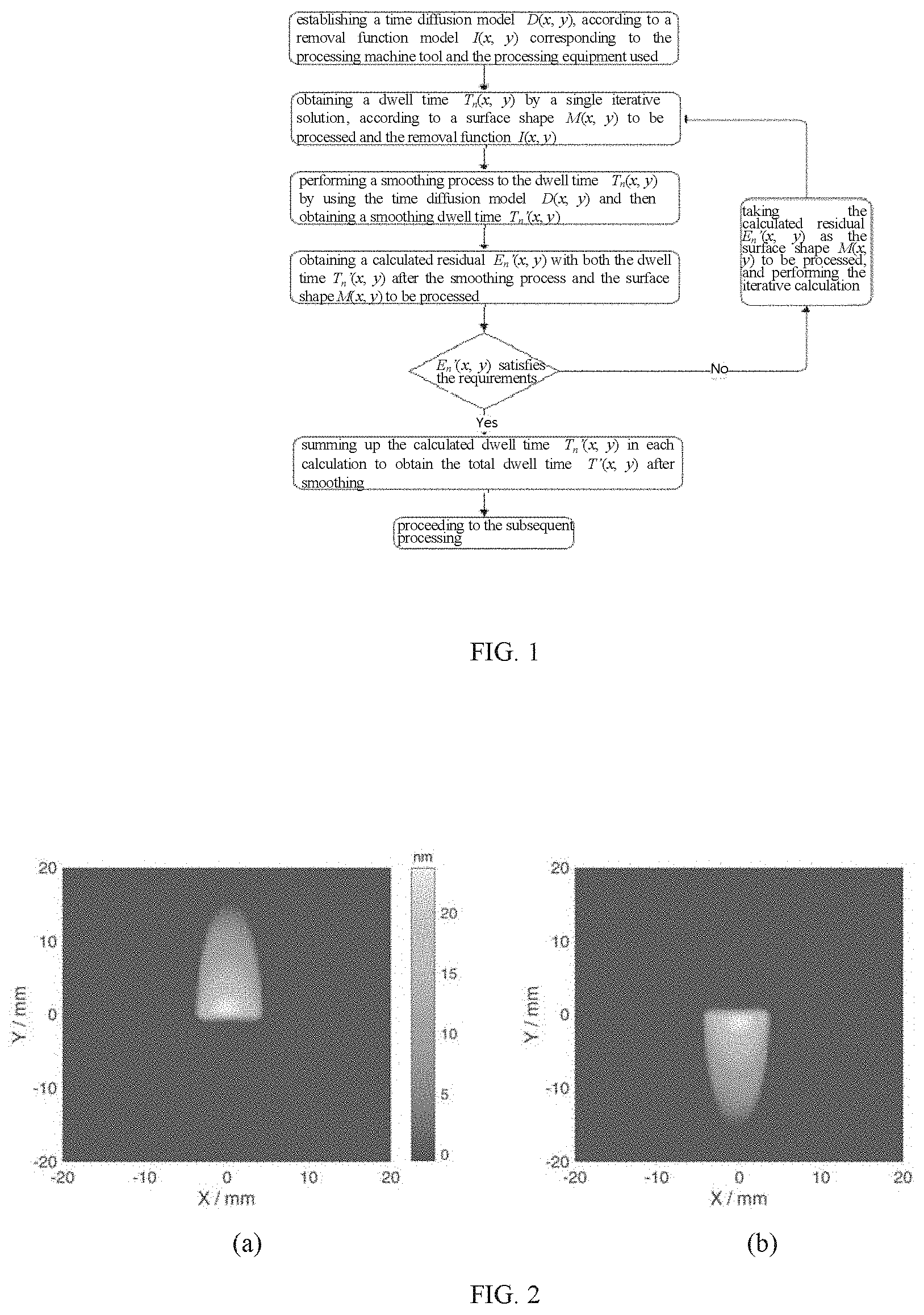
Foreign Application Data
| Date | Code | Application Number |
|---|---|---|
| Nov 12, 2018 | CN | 201811336114.8 |
Claims
1. A method for smoothing a dwell time during a processing to an optical component, wherein the dwell time of the polishing tool at each discrete point on a surface of the optical component is controlled such that a distribution of the dwell time on the surface is smoothened, and a smoothing control to the dwell time is achieved by a diffusion transformation to the distribution of the dwell time using a time diffusion model, in which the method comprises: (a) establishing a time diffusion model D(x, y) with a center position D(x.sub.0, y.sub.0), and D(x, y) satisfies a requirement for normalization to the total amount: .SIGMA..sub.i,jD(x.sub.i,y.sub.j)=1 (1) (b) a surface shape error of the component to be processed is M(x, y), and a removal function of the polishing tool in a unit time is I(x, y), and in an iterative calculation process, a dwell time obtained by a single iteration solution is T.sub.1(x, y); in the dwell time T.sub.1(x, y), a difference between a theoretical removal amount and the surface shape error M(x, y) of the component to be processed is a calculated residual E.sub.1(x, y), which can be expressed as: E.sub.1(x,y)=M(x,y)-T.sub.1(x,y)**I(x,y) (2) where ** denotes a convolution, T.sub.1(x, y)**I(x, y) denotes a removal amount of the component to be processed by the polishing tool during the dwell time T.sub.1(x, y); (c) for each discrete coordinate point (x.sub.i, y.sub.j) in T.sub.1(x, y), the time diffusion model D(x, y) is translated in both X and Y directions so that its center position (x.sub.0, y.sub.0) is moved to (x.sub.i, y.sub.j) and is expressed as D.sub.ij(x, y): D.sub.ij(x,y)=D(x-x.sub.i,y-y.sub.j) (3) subsequently, performing a point-to-surface diffusion process to the point T.sub.1(x.sub.i, y.sub.j) with the diffusion function D.sub.ij(x, y), thereby obtaining a post-diffusion time distribution K.sub.ij(x, y): K.sub.ij(x,y)=D.sub.ij(x,y)T.sub.1(x.sub.i,y.sub.j) (4) since D.sub.ij(x, y) also satisfies the requirement for normalization to the total amount as in equation (1), so there are: .SIGMA..sub.i,jK.sub.ij(x,y)=T.sub.1(x.sub.i,y.sub.j) (5) k.sub.ij(x,y)**I(x,y).apprxeq.T.sub.1(x.sub.i,y.sub.j)I(x,y) (6) (d) according to those described in said (c), obtaining a post-diffusion time distribution K.sub.ij(x, y) for each discrete point (x.sub.i, y.sub.j), and the dwell time distribution T.sub.1'(x, y) after smoothing can be expressed as: T.sub.1'(x,y)=.SIGMA..sub.i,jK.sub.ij(x,y) (7) and the removal amount corresponding to the dwell time distribution T.sub.1'(x, y) after smoothing should be approximately equal to the removal amount corresponding to the dwell time distribution T.sub.1(x, y) before smoothing: T.sub.1'(x,y)**I(x,y).apprxeq.T.sub.1(x,y)**I(x,y) (8) (e) a difference between the surface shape error M(x, y) of the component to be processed and the removal amount corresponding to the dwell time T.sub.1'(x, y) after smoothing is a calculation residual E.sub.1'(x, y) of the dwell time by a single iteration solution after smoothing: E.sub.1'(x,y)=M(x,y)-T.sub.1'(x,y)**I(x,y) (9) (f) selecting the calculation residual E.sub.1' as the surface shape error M of the component to be processed, and repeating said (b) to (e), and performing iterative calculations, until the calculation of the n.sub.th iteration is completed, and the corresponding calculated residual E.sub.n' satisfies the requirement, thereby obtaining a total dwell time distribution T'(x, y) after smoothing: T'(x,y)=.SIGMA..sub.k=1.sup.nT.sub.k'(x,y) (10) where n denotes a total number of iteration cycles; thereby achieving a smoothing processing to the dwell time during a processing to the optical component.
2. The method according to claim 1, wherein the performing of a smoothing control to the dwell time using a time diffusion model, includes adjusting the time diffusion model to improve the smoothing effect of the dwell time, wherein a shape of the removal function I(x, y) being normalized after rotating the removal function I(x, y) by 180 degrees is normalized to be the time diffusion model D(x, y).
Description
INCORPORATION BY REFERENCE TO ANY PRIORITY APPLICATIONS
[0001] Any and all applications for which a foreign or domestic priority claim is identified in the Application Data Sheet as filed with the present application are hereby incorporated by reference.
BACKGROUND OF THE INVENTION
Field of the Invention
[0002] The embodiment of the present disclosure relates to a method for smoothing a dwell time during a processing to an optical component, which belongs to a field of processing the optical component.
Description of the Related Art
[0003] With a rapid development of optical technology and a continuous expansion of its application range, people have put forward higher and higher requirements on technical indicators of the optical components, such as the surface shape precision and surface roughness. An aspherical surface, a relatively large caliber, and a nanometer-order precision become development trends of modern optical components. In order to effectively improve the surface processing quality of optical components and to meet the requirements of modern high-precision machining technology, technicians have begun to use high-precision numerically controlled machining tools to process optical components. In the numerically controlled machining process, a polishing tool of a high-precision numerically controlled machining tool applies a certain relative movement speed and a certain pressure on the surface of the components to be processed so as to remove excess material on the surface of the components to be processed. Due to the introduction of digital technology, a moving trajectory of the polishing tool on the surface of the component to be processed can be approximated as a continuous movement at various discrete points. In a unit time, a removal amount of the components to be processed at a single discrete point by the polishing tool is defined as a removal function, while the time in which the polishing tool dwells at each discrete point is defined as a dwell time. Therefore, how to plan a distribution of the dwell time of the polishing tool on the surface of the components to be processed is a key point to achieve a high-precision numerical controlled machining.
[0004] In the relevant art, a method for solving the dwell time mainly comprises a overall optimal solution and a local optimal solution:
[0005] 1. Overall Optimal Solution
[0006] In a condition that the removal function and the removal amount of the component to be processed are given, a set of optimal dwell time distributions can be calculated by a classical algorithm such as least square method and the like to minimize a surface shape error of the surface of the component after processing, then such a set of the optimal dwell time distributions is the overall optimal solution. However, in an actual high-precision machining, the amount of data and the amount of calculation involved in the calculation process are very large, which makes it difficult to obtain an overall optimal solution.
[0007] 2. Local Optimal Solution
[0008] In order to calculate a set of better dwell time distributions in a limited time, which makes the surface shape error of the surface of the component after processing to be as small as possible, algorithms such as a proportional estimation iteration method, a pulse iteration method and the like are usually used to solve the dwell time, and such a set of dwell time distributions is the local optimal solution. However, this method is mainly applicable to the case where the removal function of the polishing tool on the surface of the component is circularly symmetric. In a condition of the polishing device, such as a magnetorheological polishing machine and the like whose removal function is non-circularly symmetric, a convergence effect in the computation of the method is still to be improved.
[0009] However, neither of the above methods takes a smoothing problem of the dwell time distribution into account; in a condition that the dwell time variation between each two adjacent discrete points is too large, that is, the dwell time distribution is not smoothing enough, it is likely that the polishing tool accelerates or decelerates frequently during the movement thereof, thereby adversely affecting the stability of the machine tool, and thus leaving a movement trail on the surface of the machined component. Normally, the movement trail has a spatial size on the order of a spacing between any two adjacent discrete points, i.e., the spatial size corresponds to a medium frequency surface shape error and/or a high frequency surface shape error. Since the surface shape error is introduced during the processing to the processing equipment, and a correction to the medium frequency surface shape error and the high frequency surface shape error is a technical difficulty in the current numerical control processing, then they are difficult to be corrected by a secondary processing.
SUMMARY OF THE INVENTION
[0010] The object of the present disclosure is to overcome deficiencies in relevant art and to provide a method for smoothing the dwell time of an optical component during processing thereto. In the method, the dwell time distribution obtained by calculation in an iterative process through a local optimal solution is diffused by introducing a time diffusion model, thereby achieve a smoothing process to the dwell time, which inherits the advantages of the local optimal solution, while the calculation amount is much smaller than an overall optimal solution.
[0011] A method for smoothing a dwell time during a processing to an optical component, which specifically comprises following steps:
[0012] Step 1: establishing a time diffusion model D(x, y) with a center position D(x.sub.0, y.sub.0), and D(x, y) satisfies a requirement for normalization to the total amount:
.SIGMA..sub.i,jD(x.sub.i,y.sub.j)=1 (1)
[0013] Step 2: a surface shape error of the component to be processed is M(x, y), and a removal function of the polishing tool in a unit time is I(x, y), and in an iterative calculation process, a dwell time obtained by a single iteration solution is T.sub.1(x, y); in the dwell time T.sub.1(x, y), a difference between a theoretical removal amount and the surface shape error M(x, y) of the component to be processed is a calculated residual E.sub.1(x, y), which can be expressed as:
E.sub.1(x,y)=M(x,y)-T.sub.1(x,y)**I(x,y) (2)
where ** denotes a convolution, T.sub.1(x, y)**I(x, y) denotes a removal amount of the component to be processed by the polishing tool during the dwell time T.sub.1(x, y);
[0014] Step 3: for each discrete coordinate point (x.sub.i, y.sub.j) in T.sub.1(x, y), the time diffusion model D(x, y) is translated in both X and Y directions so that its center position (x.sub.0, y.sub.0) is moved to (x.sub.i, y.sub.j) and is expressed as D.sub.ij(x, y):
D.sub.ij(x,y)=D(x-x.sub.i,y-y.sub.j) (3)
[0015] subsequently, performing a point-to-surface diffusion process to the point T.sub.1(x.sub.i, y.sub.j) with the diffusion function D.sub.ij(x, y), thereby obtaining a post-diffusion time distribution K.sub.ij(x, y):
K.sub.ij(x,y)=D.sub.ij(x,y)T.sub.1(x.sub.i,y.sub.j) (4)
[0016] since D.sub.ij(x, y) also satisfies the requirement for normalization to the total amount as in equation (1), so there are:
.SIGMA..sub.i,jK.sub.ij(x,y)=T.sub.1(x.sub.i,y.sub.j) (5)
k.sub.ij(x,y)**I(x,y).apprxeq.T.sub.1(x.sub.i,y.sub.j)I(x,y) (6)
[0017] Step 4: according to those described in Step 3, obtaining a post-diffusion time distribution K.sub.ij(x, y) for each discrete point (x.sub.i, y.sub.j), and the dwell time distribution T.sub.1'(x, y) after smoothing can be expressed as:
T.sub.1'(x,y)=.SIGMA..sub.i,jK.sub.ij(x,y) (7)
and the removal amount corresponding to the dwell time distribution T.sub.1'(x, y) after smoothing should be approximately equal to the removal amount corresponding to the dwell time distribution T.sub.1(x, y) before smoothing:
T.sub.1'(x,y)**I(x,y).apprxeq.T.sub.1(x,y)**I(x,y) (8)
[0018] Step 5: a difference between the surface shape error M(x, y) of the component to be processed and the removal amount corresponding to the dwell time T.sub.1'(x, y) after smoothing is a calculation residual E.sub.1'(x, y) of the dwell time by a single iteration solution after smoothing:
E.sub.1'(x,y)=M(x,y)-T.sub.1'(x,y)**I(x,y) (9)
[0019] Step 6: selecting the calculation residual E.sub.1' as the surface shape error M of the component to be processed, and repeating Step 2 to Step 5, and performing iterative calculations, until the calculation of a n.sub.th iteration is completed, and the corresponding calculated residual E.sub.n' satisfies the requirement, thereby obtaining a total dwell time distribution T'(x, y) after smoothing:
T'(x,y)=.SIGMA..sub.k=1.sup.nT.sub.k'(x,y) (10)
where n denotes a total number of iteration cycles; thereby achieving a smoothing processing to the dwell time during a processing to the optical component.
[0020] In an embodiment, the step of performing a smoothing control to the dwell time using a time diffusion model, includes adjusting the time diffusion model to improve the smoothing effect of the dwell time, wherein a shape of the removal function I(x, y) after rotating the removal function I(x, y) by 180 degrees is normalized to be the time diffusion model D(x, y).
[0021] The advantages and beneficial technical effects of the present disclosure over the prior art are as follows:
[0022] 1. The method for smoothing the dwell time during a processing to an optical component according to the present disclosure may achieve a compensate effect in case where the removal function of the polishing tool on the surface of the component is non-circularly symmetric, and improve the convergence effect of the iterative calculation.
[0023] 2. The method for smoothing the dwell time during a processing to an optical component according to the present disclosure may reduce a degree of jump of the dwell time between adjacent discrete points by smoothing the dwell time in the iterative calculation process, thereby reducing the adverse effect on the stability of the machine tool due to the frequent acceleration or deceleration of the polishing tool during the processing, thereby reducing the medium and high frequency surface shape errors introduced by the equipment to the component to be processed during the machining process.
BRIEF DESCRIPTION OF THE DRAWINGS
[0024] FIG. 1 is a flow chart for performing a method for smoothing a dwell time during a processing to an optical component according to the present disclosure;
[0025] FIG. 2(a) is the removal function distribution used in the embodiment, and FIG. 2(b) is the time diffusion model used in the embodiment;
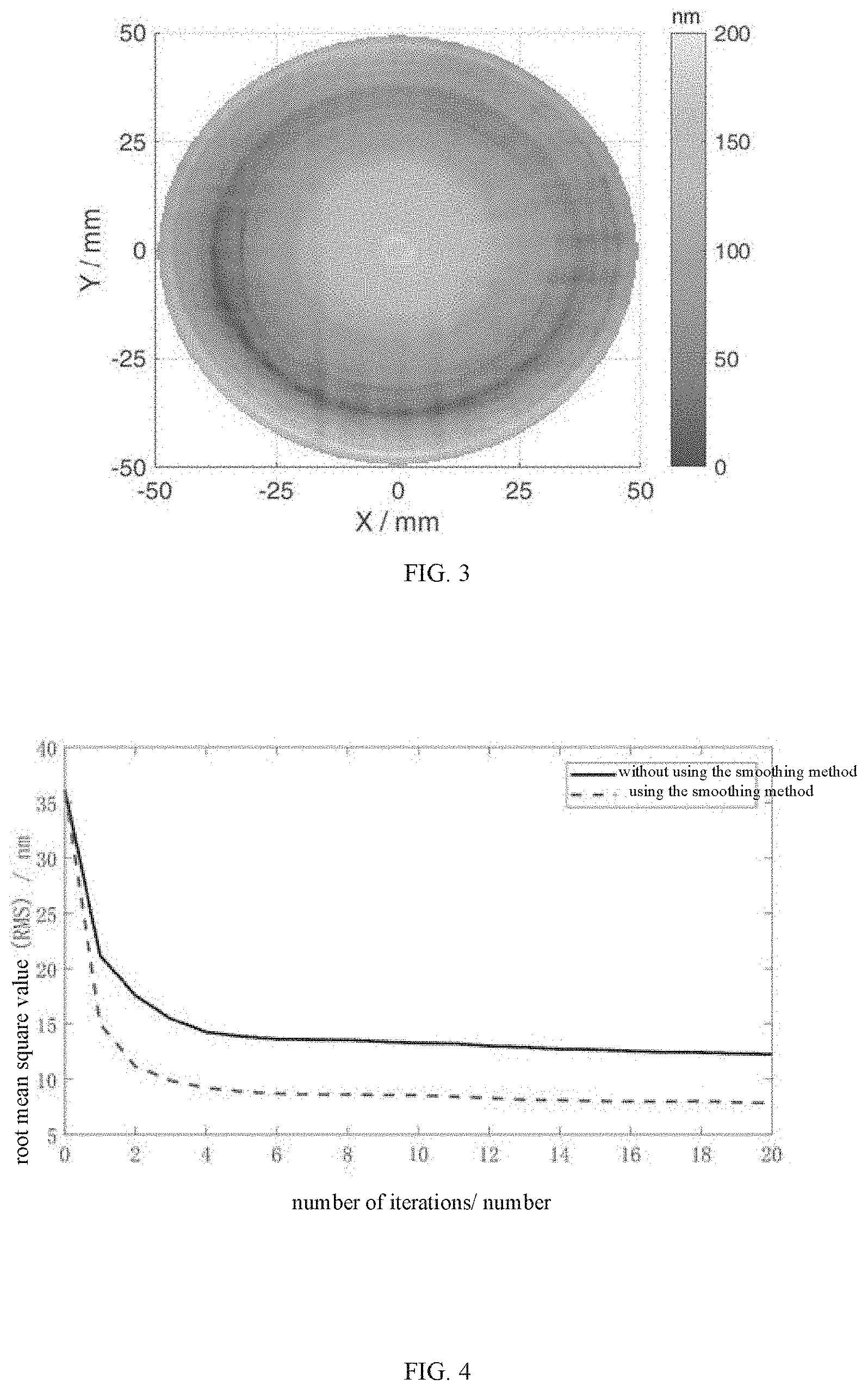
[0026] FIG. 3 is an initial shape error to be processed in the embodiment;
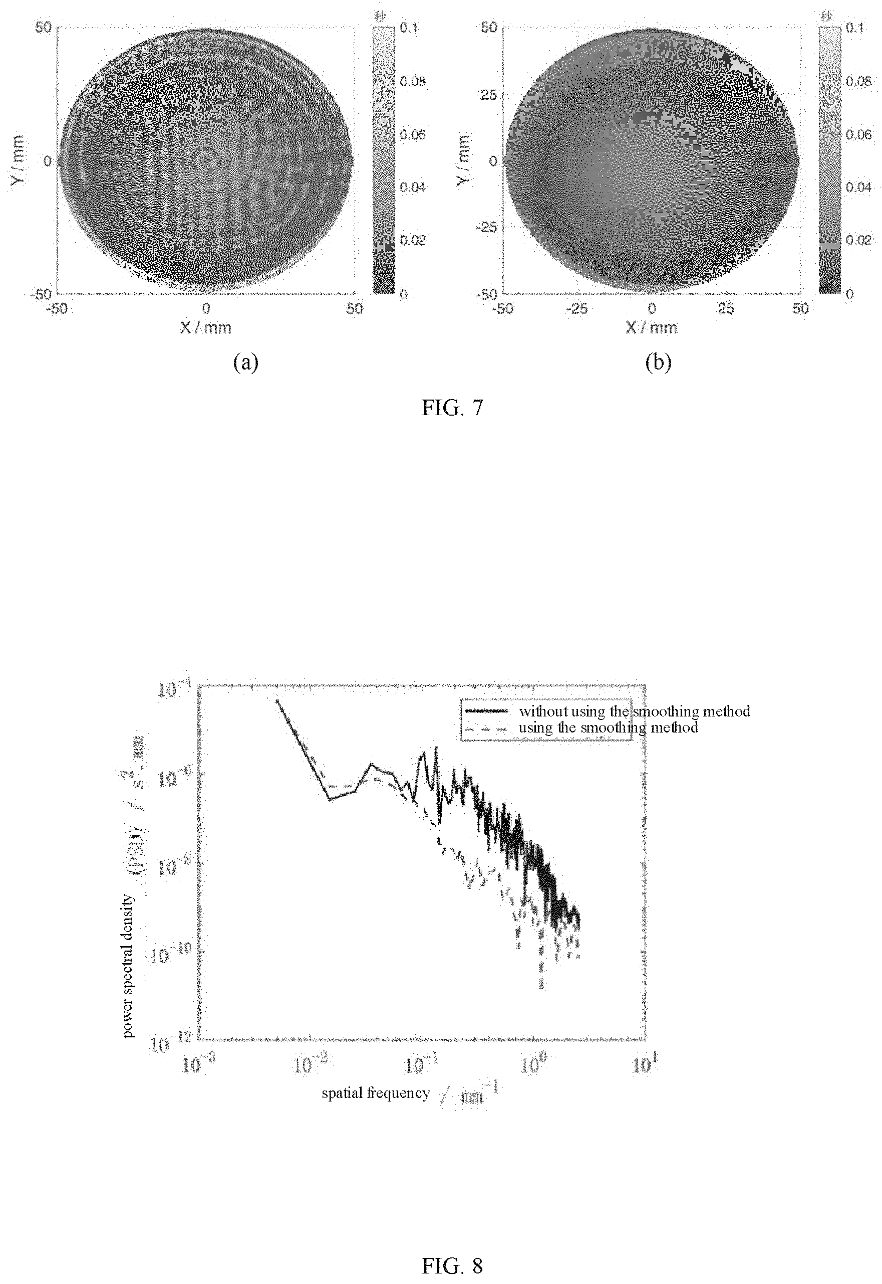
[0027] FIG. 4 is a graph showing a variation trend of the root mean square value (RMS) of the calculated residual as a function of the number of iterations in the embodiment, in which the solid line is a variation trend of the root mean square value (RMS) of the calculated residual as a function of the number of iterations without using the method for smoothing a dwell time during a processing to an optical component according to the present disclosure, while the dashed line is a variation trend of the root mean square value (RMS) of the calculated residual as a function of the number of iterations using the method for smoothing a dwell time during a processing to an optical component according to the present disclosure.
[0028] FIG. 5 (a)(b) are comparison diagrams of the calculated residuals in the embodiment, in which FIG. 5(a) is the calculated residual without using the method for smoothing a dwell time during a processing to an optical component according to the present disclosure, and FIG. 5(b) is the calculated residual using the method for smoothing a dwell time during a processing to an optical component according to the present disclosure;
[0029] FIG. 6 is a power spectral density (PSD) distribution of the calculated residual in the embodiment, in which the solid line is the power spectral density (PSD) distribution of the calculated residual without using the method for smoothing a dwell time during a processing to an optical component according to the present disclosure, and the dashed line is the power spectral density (PSD) distribution of the calculated residual using the method for smoothing a dwell time during a processing to an optical component according to the present disclosure.
[0030] FIG. 7 (a)(b) are comparison diagrams of the dwell time obtained by iterative calculation in the embodiment, in which FIG. 7 (a) is a dwell time distribution without using the method for smoothing a dwell time during a processing to an optical component according to the present disclosure, FIG. 7 (b) is a dwell time distribution using the method for smoothing a dwell time during a processing to an optical component according to the present disclosure.
[0031] FIG. 8 is a power spectral density (PSD) distribution of the dwell time in an embodiment, in which the solid line is the power spectral density (PSD) distribution of the dwell time without using the method for smoothing a dwell time during a processing to an optical component according to the present disclosure, and the dashed line is the power spectral density (PSD) distribution of dwell time using the method for smoothing a dwell time during a processing to an optical component according to the present disclosure.
DETAILED DESCRIPTION OF THE PREFERRED EMBODIMENT
[0032] The present disclosure will be further described in detail with reference to the accompanying drawings. It is to be understood that the described embodiments are only intended to be a further description of the disclosure, and are not intended to limit the scope of the disclosure. The flow chart for implementing the method for smoothing a dwell time during a processing to an optical component proposed by the present disclosure is as shown in FIG. 1.
[0033] In the first step, establishing a time diffusion model D(x, y) used in the method for smoothing a dwell time during a processing to an optical component time in the processing of an optical component of the present disclosure, according to a removal function model I(x, y) corresponding to the processing machine tool and the processing equipment used;
[0034] In the second step, obtaining a dwell time T.sub.n(x, y) by a single iterative solution, according to a surface shape M(x, y) to be processed and the removal function I(x, y);
[0035] In the third step, performing a smoothing process to the dwell time T.sub.n(x, y) by using the time diffusion model D(x, y), and then obtaining a smoothing dwell time T.sub.n'(x, y);
[0036] In the fourth step, obtaining a calculated residual E.sub.n'(x, y) with both the dwell time T.sub.n'(x, y) after the smoothing process and the surface shape M(x, y) to be processed;
[0037] In the fifth step, taking the calculated residual E.sub.n'(x, y) as the surface shape M(x, y) to be processed, and repeating the second step to the fourth step, and performing the iterative calculation, until the calculated residual E.sub.n'(x, y) satisfies the requirements after finishing the nth iteration calculation;
[0038] In the sixth step, summing up the calculated dwell time T.sub.n'(x, y) in each calculation to obtain the total dwell time T'(x, y) after smoothing, and in turn proceeding to the subsequent processing.
EMBODIMENTS
[0039] In this embodiment, a magnetorheological numerical control polishing machine is used as a processing device, and a circular flat mirror having a diameter of 100 mm is used as a component to be processed, and a specific embodiment of the present disclosure is exemplified in conjunction with FIG. 2 to FIG. 7. In the following description, the method for smoothing a dwell time during a processing to an optical component according to the present disclosure is simply referred to as a smoothing method. Under normal circumstances, the removal function of the magnetorheological polishing machine is non-circularly symmetric.
[0040] FIG. 2(a) shows the removal function distribution I(x, y) of the magnetorheological polishing head dwell at the coordinate point of x=0, y=0 for 3 seconds. In this embodiment, the shape distribution of the removal function distribution after being rotated by 180 degrees with respect to a coordinate point of x=0, y=0 may function as a time diffusion model D(x, y), and its distribution pattern is shown in FIG. 2(b); and the total amount of the time diffusion model is normalized to satisfy the equation (1).
[0041] FIG. 3 is an initial shape error M(x, y) of the component to be processed, whose peak-to-valley value (PV) of the surface shape is 200.076 nm, and the root mean square value (RMS) is 36.115 nm. By substituting both the surface shape error M(x, y) to be processed and the removal function I(x, y) into the equation (2), the dwell time distribution T.sub.1(x, y) and the corresponding calculated residual E.sub.1(x, y) will be obtained without using the smoothing method. For the above-mentioned dwell time T.sub.1(x, y), using the time diffusion model D(x, y) shown in FIG. 2(b) to perform smoothing process according to the equations (3).about.(8), and then the dwell time distribution T.sub.1'(x, y) after using the smoothing method can be obtained, and the calculated residual E.sub.1'(x, y) after using the smoothing method is calculated by the equation (9).
[0042] When the smoothing method is not used, the above-mentioned calculated residual E.sub.1(x, y) is taken as the surface shape error M(x, y) to be processed, and it is substituted into the cycle for iterative calculation; when the smoothing method is used, the above-mentioned calculated residual E.sub.1'(x, y) is taken as the surface shape error M(x, y) to be processed, and it is substituted into the cycle for iterative calculation.
[0043] FIG. 4 shows the variation trend of the root mean square (RMS) of the calculated residual as a function of the number of iterations in the 20 iterations calculation, in which the solid line is a variation trend of the root mean square value (RMS) of the calculated residual as a function of the number of iterations without using the smoothing method, while the dashed line is a variation trend of the root mean square value (RMS) of the calculated residual as a function of the number of iterations using the smoothing method. It can be seen from FIG. 4 that, the root mean square value (RMS) of the calculated residuals tends to decrease gradually with an increase in the number of iterations, and after using the smoothing method, the convergence speed and convergence effect of the root mean square value (RMS) of the calculated residual are better than those without using the smoothing method. When the smoothing method is not used, the calculated residual E.sub.20(x, y) after the completion of the 20.sub.th iteration is shown in FIG. 5(a), and the corresponding peak-to-valley (PV) value is 96.258 nm, and the root mean square value is (RMS) is 12.263 nm; and after using the smoothing method, the calculated residual E.sub.20'(x, y) after the completion of the 20.sub.th iteration is shown in FIG. 5(b), and the corresponding peak-to-valley (PV) value is 86.432 nm, root mean square (RMS) is 7.835 nm. Compared with FIG. 5(a), the surface shape distribution corresponding to FIG. 5(b) is more uniform and more gentle, and its peak-to-valley (PV) value and root mean square (RMS) values are also smaller, which indicates that the smoothing method can improve the convergence effect of the iterative calculation, even if the removal function of the polishing tool on the surface of the component is a non-circular symmetric distribution, a better convergence effect can be achieved after using the smoothing method. As shown in FIG. 6, the power spectral density (PSD) distribution of the calculated residual E.sub.20(x, y) without using the smoothing method is compared with the power spectral density (PSD) distribution of the calculated residual E.sub.20(x, y) using the smoothing method. The power spectral density (PSD) is well known in the art and will not be further described here. The numerical equation is:
PSD = .DELTA. x n n = 0 N - 1 M ( n ) e - i 2 .pi. f m n .DELTA. x ( 11 ) ##EQU00001##
[0044] where .quadrature. .DELTA.x=L/N is a sampling interval, L is a sampling length, N is an effective sampling point number, and M(n) is an error function. It can be seen from FIG. 6 that, compared with the case in which the smoothing method is not used, after using the smoothing method, the portion of the calculated residual surface shape with a spatial frequency less than 0.2 mm.sup.-1 (which usually corresponds to the medium frequency error and/or low frequency error) is reduced, which in turn indicates that the smoothing method can improve the processing effect of the processing equipment in the middle and low frequency portions.
[0045] FIG. 7 shows a comparison of the dwell time distributions solved without using the smoothing method and using the smoothing method, in which the spatial size corresponding to each discrete point is 0.0383 mm.sup.2, that is, 512.times.512 discrete points are used to perform a discrete processing on a square area with a side length of 100 mm; FIG. 7(a) is the total dwell time T(x, y) distribution obtained after completion of the 20.sub.th iterative calculation without using the smoothing method. T(x, y) satisfies T(x, y)=.SIGMA..sub.k=1.sup.20 T.sub.k(x, y), the corresponding peak-to-valley (PV) value is 0.107 seconds, and the root mean square value (RMS) is 0.013 seconds; FIG. 7(b) is the total dwell time T'(x, y) distribution obtained after completion of the 20.sub.th iterative calculation using the smoothing method. T'(x, y) satisfies T'(x, y)=.SIGMA..sub.k=1.sup.20 T.sub.k'(x, y), the corresponding peak-to-valley (PV) value is 0.038 seconds, and the root mean square value (RMS) is 0.006 seconds. It can be seen that the dwell time calculated using the smoothing method has a peak-to-valley (PV) and root mean square (RMS) ratio which are reduced when compared to those of the calculated dwell time without using the smoothing method, and the time distribution is more uniform and more gentle. FIG. 8 compares the distribution characteristics of the dwell times T(x, y) and T'(x, y) at spatial frequencies from the perspective of power spectral density. It can be seen from FIG. 8 that the portions whose spatial frequency is higher than 0.05 mm.sup.-1 (usually corresponding to the medium frequency error and/or high frequency error) in the dwell time distribution using the smoothing method are reduced compared to the case where the smoothing method is not used, which shows that utilization of smoothing method can reduce the level of the frequent movement of the polishing tool in a small space, thereby reducing the medium and high frequency errors introduced into the components due to frequent shaking of the polishing tool during the processing.
[0046] Through the above embodiments, it is shown that the method for smoothing a dwell time during a processing to an optical component according to the present disclosure can improve the convergence effect of the iterative calculation in the process of calculating the dwell time, and improve the capability of correcting the medium and high frequency surface shape error of the processing equipment to the surface of the component to be processed. In addition, the method for smoothing the dwell time during the processing to an optical component of the present disclosure can limit the degree of jump of the dwell time between adjacent discrete points by smoothing the dwell time, thereby reducing the adverse effect on the stability of a numerical control machining due to the frequent acceleration or deceleration of the polishing tool during the processing, thereby reducing medium and high frequency errors introduced into the components due to frequent shaking of the polishing tool.
* * * * *
uspto.report is an independent third-party trademark research tool that is not affiliated, endorsed, or sponsored by the United States Patent and Trademark Office (USPTO) or any other governmental organization. The information provided by uspto.report is based on publicly available data at the time of writing and is intended for informational purposes only.
While we strive to provide accurate and up-to-date information, we do not guarantee the accuracy, completeness, reliability, or suitability of the information displayed on this site. The use of this site is at your own risk. Any reliance you place on such information is therefore strictly at your own risk.
All official trademark data, including owner information, should be verified by visiting the official USPTO website at www.uspto.gov. This site is not intended to replace professional legal advice and should not be used as a substitute for consulting with a legal professional who is knowledgeable about trademark law.