Digital Average Input Current Control in Power Converter
Fishelov; Amir ; et al.
U.S. patent application number 16/675870 was filed with the patent office on 2020-05-07 for digital average input current control in power converter. The applicant listed for this patent is Solaredge Technologies Ltd.. Invention is credited to Amir Fishelov, Meir Gazit, Nikolay Radimov.
| Application Number | 20200144919 16/675870 |
| Document ID | / |
| Family ID | 40345855 |
| Filed Date | 2020-05-07 |


View All Diagrams
| United States Patent Application | 20200144919 |
| Kind Code | A1 |
| Fishelov; Amir ; et al. | May 7, 2020 |
Digital Average Input Current Control in Power Converter
Abstract
A digital average-input current-mode control loop for a DC/DC power converter. The power converter may be, for example, a buck converter, boost converter, or cascaded buck-boost converter. The purpose of the proposed control loop is to set the average converter input current to the requested current. Controlling the average input current can be relevant for various applications such as power factor correction (PFC), photovoltaic converters, and more. The method is based on predicting the inductor current based on measuring the input voltage, the output voltage, and the inductor current. A fast cycle-by-cycle control loop may be implemented. The conversion method is described for three different modes. For each mode a different control loop is used to control the average input current, and the control loop for each of the different modes is described. Finally, the algorithm for switching between the modes is disclosed.
| Inventors: | Fishelov; Amir; (Tel Aviv, IL) ; Gazit; Meir; (Ashkelon, IL) ; Radimov; Nikolay; (Holon, IL) | ||||||||||
| Applicant: |
|
||||||||||
|---|---|---|---|---|---|---|---|---|---|---|---|
| Family ID: | 40345855 | ||||||||||
| Appl. No.: | 16/675870 | ||||||||||
| Filed: | November 6, 2019 |
Related U.S. Patent Documents
| Application Number | Filing Date | Patent Number | ||
|---|---|---|---|---|
| 16149679 | Oct 2, 2018 | 10516336 | ||
| 16675870 | ||||
| 15495301 | Apr 24, 2017 | 10116217 | ||
| 16149679 | ||||
| 14324820 | Jul 7, 2014 | 9673711 | ||
| 15495301 | ||||
| 13661503 | Oct 26, 2012 | 8773092 | ||
| 14324820 | ||||
| 12187335 | Aug 6, 2008 | 8319483 | ||
| 13661503 | ||||
| 60954354 | Aug 7, 2007 | |||
| 60954261 | Aug 6, 2007 | |||
| Current U.S. Class: | 1/1 |
| Current CPC Class: | H02M 3/157 20130101; Y02E 10/56 20130101; H02M 3/1582 20130101 |
| International Class: | H02M 3/158 20060101 H02M003/158; H02M 3/157 20060101 H02M003/157 |
Claims
1-20. (canceled)
21. A method comprising: transferring a converter from a first mode of operation to a second mode of operation based on a duty cycle being above a first value for at least a first period of time.
22. The method of claim 21, further comprising: transferring the converter from the second mode of operation to the first mode of operation based on the duty cycle being below a second value for at least a second period of time.
23. The method of claim 21, wherein the transferring the converter from the first mode of operation to the second mode of operation comprises transferring the converter from a buck mode to a buck-boost mode based on the duty cycle being above the first value for at least the first period of time.
24. The method of claim 21, wherein the transferring the converter from the first mode of operation to the second mode of operation comprises transferring the converter from a buck-boost mode to a boost mode based on the duty cycle being above the first value for at least the first period of time.
25. The method of claim 21, further comprising controlling an input current to the converter based on a sampled input voltage or a sampled inductor current.
26. The method of claim 21, wherein the converter comprises a cascaded buck boost converter.
27. The method of claim 21, further comprising: determining that the duty cycle has been above the first value for at least the first period of time, wherein the first period of time comprises a first predetermined number of cycles.
28. A method comprising: transferring a converter from a first mode of operation to a second mode of operation based on a duty cycle being below a first value for at least a first period of time.
29. The method of claim 28, further comprising: transferring the converter from the second mode of operation to the first mode of operation based on the duty cycle being above a second value for at least a second period of time.
30. The method of claim 28, wherein the transferring the converter from the first mode of operation to the second mode of operation comprises transferring the converter from a boost mode to a buck-boost mode based on the duty cycle being below the first value for at least the first period of time.
31. The method of claim 28, wherein the transferring the converter from the first mode of operation to the second mode of operation comprises transferring the converter from a buck-boost mode to a buck mode based on the duty cycle being below the first value for at least the first period of time.
32. The method of claim 28, further comprising controlling an input current to the converter based on a sampled input voltage or a sampled inductor current.
33. The method of claim 28, wherein the converter comprises a cascaded buck boost converter.
34. The method of claim 28, further comprising: determining that the duty cycle has been below the first value for at least the first period of time, wherein the first period of time comprises a first predetermined number of cycles.
35. An apparatus comprising: a controller configured to transfer a converter from a first mode of operation to a second mode of operation based on a duty cycle being above a first value for at least a first period of time.
36. The apparatus of claim 35, wherein the controller is further configured to transfer the converter from the second mode of operation to the first mode of operation based on the duty cycle being below a second value for at least a second period of time.
37. The apparatus of claim 35, wherein the first mode of operation comprises a buck mode and the second mode of operation comprises a buck-boost mode.
38. The apparatus of claim 35, wherein the first mode of operation comprises a buck-boost mode and the second mode of operation comprises a boost mode.
39. The apparatus of claim 35, wherein the controller is further configured to: control an input current to the converter based on a sampled input voltage or a sampled inductor current, wherein the converter comprises a cascaded buck boost converter.
40. The apparatus of claim 35, wherein the controller is further configured to: determine that the duty cycle has been above the first value for at least the first period of time.
Description
RELATED APPLICATIONS
[0001] This Application claims priority from U.S. Provisional Application No. 60/954,261 filed on Aug. 6, 2007 and U.S. Provisional Application No. 60/954,354 filed on Aug. 7, 2007.
BACKGROUND
[0002] The subject invention relates to control loops for switching converters. The following articles and patents, which may or may not be prior art, and which are incorporated here by reference, may be relevant to the subject invention. [0003] Jingquan Chen, Aleksandar Prodic, Robert W. Erickson and Dragan Maksimovic, "Predictive Digital Current Programmed Control". IEEE Transaction on Power Electronics, Vol. 18, No. 1, January 2003 [0004] U.S. Pat. No. 7,148,669, "Predictive Digital Current Controllers for Switching Power Converters" by Dragan Maksimovic, Jingquan Chen, Aleksandar Prodic, and Robert W. Erickson. [0005] K Wallace, G Mantov, "DSP Controlled Buck/Boost Power Factor Correction for Telephony Rectifiers". INTELEC 2001, 14-18 Oct. 2001. [0006] U.S. Pat. No. 6,166,527, "Control Circuit and Method for Maintaining High Efficiency in a Buck-Boost Switching Regulator" by David M. Dwelley, and Trevor W. Barcelo.
[0007] Additionally, the following basic text is incorporated here by reference, in order to provide the reader with relevant art and definitions: [0008] Robert W. Erickson, Dragan Maksimovic, "Fundamentals of Power Electronics" (Second Edition), ISBN 0792372700.
SUMMARY
[0009] Aspects of the invention provide a method and system for digitally controlling the average input current in a non-inverting buck-boost converter. The method provides a fast cycle-by-cycle control loop to set the average input current when the converter is working in three different modes: buck, buck-boost and boost. Unlike analog control where it is difficult to change the parameters of the control loop in an adaptive manner, a digital control system can adjust the control loop parameters according to various parameters measured such as input voltage, output voltage and inductor current. In general, this enables to achieve a fast and stable control loop that controls the input current in various working points of the converter.
[0010] Aspects of the invention also provide for a method and system for digitally controlling the input current in a non-inverting (cascaded) buck-boost converter operating in a buck-boost mode, i.e., alternating between buck and boost in each cycle. Such an operation mode is particularly beneficial when the required converter output current is similar to the converter's input current. Since there are limits to the maximal and minimal allowed PWM values of the buck or boost operational modes, there are areas in which control is impossible without use of the alternating buck-boost mode.
[0011] Aspects of the invention further provide for a method and system for controlling the operational mode switching of a cascaded buck-boost converter. According to aspects of the invention, whenever the converter has been operated in one mode, i.e., buck or boost, for at least a predetermined period, and is needed to change into the other operational mode, i.e., to boost or buck, the transition is performed by forcing the converter to first execute several cycles on alternating buck and boost modes and only then switching to the other mode. Thus, for example, if the converter has been operating in a buck mode and is now to be switched to a boost mode, it is first switched to operate in an alternating buck-boost mode, in which the converter alternates by each cycle between buck and boost modes for several cycles, and only then switches to boost mode. This feature avoids the current jumps or discontinuities that are generally observed when a converter switches between buck and boost modes of operation.
[0012] Aspects of the invention further provide for a method and system for controlling the operation of a cascaded buck-boost converter, operable in one of three modes: buck, boost, and alternating buck-boost. The system includes three preprogrammed PWM control modules, each for controlling the input current according to one of the converter's operational modes. During operation of the converter, the operational mode is determined and the corresponding PWM control module is selected to control the input current.
BRIEF DESCRIPTION OF THE DRAWINGS
[0013] FIG. 1 illustrate an example of a digital controlled non-inverting buck-boost converter according to aspects of the invention.
[0014] FIG. 2 illustrates the waveforms of trailing triangle PWM modulation.
[0015] FIG. 3 illustrates the waveforms of leading triangle PWM modulation.
[0016] FIG. 4 shows the inductor current waveform during two switching cycles using trailing edge triangle PWM modulation.
[0017] FIG. 5 illustrates a block diagram of predictive buck input current control, according to embodiment of the invention.
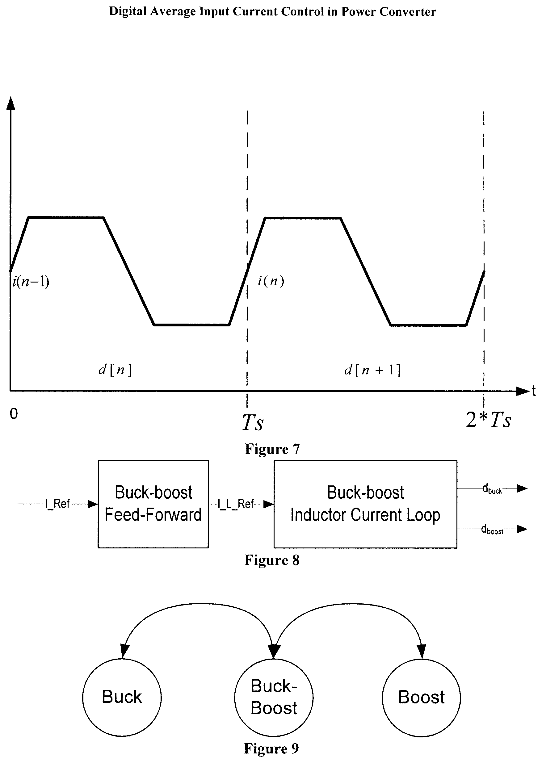
[0018] FIG. 6 illustrates the inductor current waveforms for a buck-boost switching cycle.
[0019] FIG. 7 illustrates the inductor current waveforms for a buck-boost switching cycle according to embodiment of the invention.
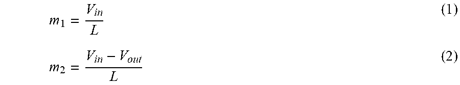
[0020] FIG. 8 shows a block diagram of control loops for buck-boost input current control, according to embodiment of the invention.
[0021] FIG. 9 shows a state diagram and the possible options to switch between the three different states.
DETAILED DESCRIPTION
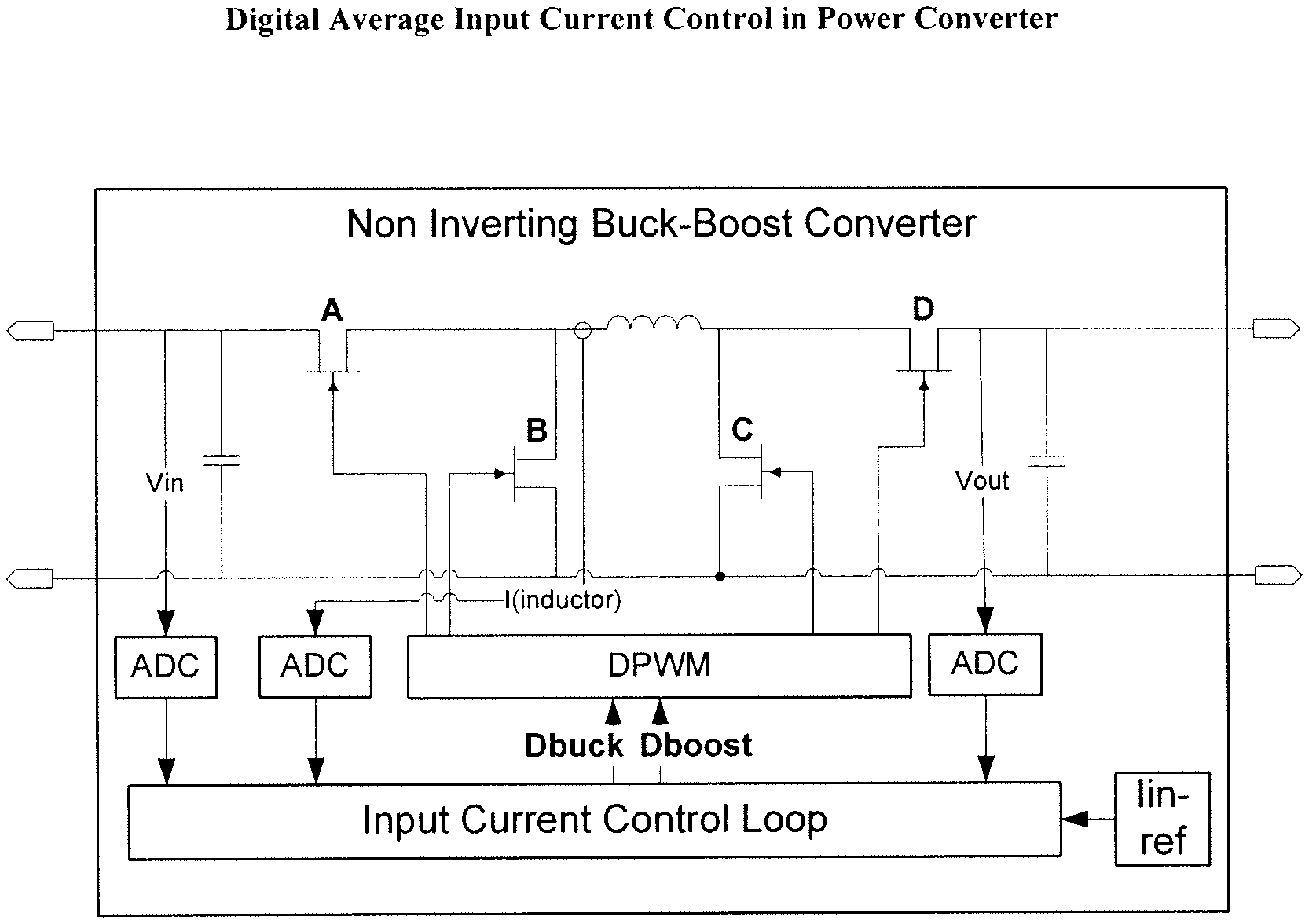
[0022] A digital controlled non-inverting (cascaded) buck-boost converter, as described in FIG. 1, is a topology for a converter that is capable of both increasing the input voltage and decreasing it. The proposed topology is beneficial over prior art converters for at least the following reasons: 1) high conversion efficiency can be achieved; 2) component stress is relatively low as apposed to other buck-boost topologies; and 3) low component count--only one inductor, two capacitors and four switches. When buck-boost converters are discussed in this specification, we typically refer to cascaded buck-boost topology, sometimes named "non-inverting buck-boost" converter, rather then the lower efficiency (inverting) buck-boost converter.
[0023] While in general control loops of converters the inductor current is controlled, according to an embodiment of the invention, a control loop is provided in order to set the average input current to the requested current (I.sub.ref). Controlling the average input current can be relevant for various applications such as: power factor correction (PFC), photovoltaic inverters, and more. In this example, the control is based on predicting the inductor current for the next switching cycle based on measuring the input voltage (V.sub.In), the output voltage (V.sub.Out) and the inductor current (I.sub.L) in the current switching cycle. By using a predictive method a fast, cycle-by-cycle, control loop can be implemented.
[0024] Converter Modes
[0025] The cascaded buck-boost topology can achieve the desired input average current at various output currents. Depending on the output current, the converter can work in 3 different modes: [0026] 1. I.sub.ref>I.sub.out: Boost Converter--Switch A is constantly conducting and switch B is not conducting. [0027] 2. I.sub.ref<I.sub.out: Buck Converter--Switch D is constantly conducting and switch C is not conducting. [0028] 3. I.sub.ref.apprxeq.I.sub.out: Buck-Boost Converter--All four switches are being used to control the input current.
[0029] Each of the three modes may have a different control schemes. The control loop will decide which control scheme is used at each switching cycle.
[0030] Predictive Average Input Current Control Using Triangle PWM Modulation
[0031] The control scheme of this example is based on predicting the inductor current for the next switching cycle based on measuring the inductor current and the input and output voltage. Based on the inductor current the control loop sets the average input current. Because of the fact that the predictive control loop is a non-linear control loop and it is executed on every PWM cycle, a high control bandwidth can be achieved.
[0032] The following sections will explain the concept of triangle PWM modulation and the three control schemes mentioned above.
[0033] Triangle PWM Modulation
[0034] There are two types of triangle PWM modulation--leading and trialing triangle modulation. FIG. 2 illustrates the waveforms of trailing triangle PWM modulation.
[0035] Each cycle, having length T.sub.s and a duty cycle of d, starts with an on-time of length d/2T.sub.s, an off-time of (1-d)T.sub.s and another on-time of the same length. Leading triangle modulation is similar but the on-time and off-times are switched, as shown in FIG. 3. Both methods are suitable for input average current control because of the fact that the average inductor current is always at the beginning of each PWM cycle. This enables the digital control loop to sample the average inductor current at fixed intervals, at the beginning of each cycle.
[0036] Controlling Average Input Current Using the Inductor Current
[0037] The method of this example uses the inductor current to set the average input current when the converting is operating in continuous conduction mode (CCM). The converter can work in one of three different modes--Buck, Boost, Buck-Boost. For each mode there is a different equation for converting the average inductor current to the average input current in each switching cycle. Derived from the power train properties of the converter, the equations are: [0038] 1. Boost: .sub.In= .sub.L [0039] 2. Buck: .sub.In= .sub.L*d, where d is the duty cycle. [0040] 3. Buck-Boost: .sub.In= .sub.L*d.sub.buck, where d.sub.buck is the buck duty cycle
[0041] For all of the equations above .sub.In, .sub.L denote the average input current and average inductor current, respectively.
[0042] Control Loops
[0043] The converter works in 3 different modes. For each mode a different control loop is used to control the average input current. This section will describe each control loop for the different modes. Later on, the algorithm for switching between the modes will be described.
[0044] Predictive Boost Input Current Control
[0045] The goal of the control loop is to insure that the average input current follows the reference I.sub.ref. As described above, when the converter operates in a boost mode the steady state average input current is the same as the average inductor current. In this mode the boost control will try to set the average inductor current to I.sub.f. The required boost duty cycle for the next switching cycle is predicted based on the sampled inductor current, the input voltage and the output voltage. FIG. 4 shows the inductor current waveform during two switching cycles using trailing edge triangle PWM modulation. The sampled inductor current at switching cycle n, i(n), can be calculated using the previous sample, i(n-1), and the input and output voltage. The calculation is based on the inductor current slopes during the on-time and off-time.
[0046] Since the input and output voltage change slowly we assume that they are constant during a switching cycle. For a boost converter the on-time slope (m.sub.1) and off-time slope (m.sub.2) are given by the following equations:
m 1 = V i n L ( 1 ) m 2 = V i n - V out L ( 2 ) ##EQU00001##
[0047] Based on these equations we can predict i(n) using the following equation:
i pred ( n ) = i ( n ) = i ( n - 1 ) + V i n d [ n ] T s L + ( V i n - V out ) d ' [ n ] T s L ( 3 ) ##EQU00002##
[0048] Where d'[n]=1-d[n], T.sub.s is the switching cycle time and L is the inductor inductance. Equation (3) can also be written as:
i pred ( n ) = i ( n ) = i ( n - 1 ) + V out d [ n ] T s L + ( V i n - V out ) T s L ( 4 ) ##EQU00003##
[0049] We now have the prediction equation for one switching cycle. Because of the fact that every digital implementation of the control loop will have an execution delay, we will extend the prediction to one more switching cycle. So the prediction will set the duty cycle of the n+1 switching cycle based on the samples of the n-1 switching cycle. Extending equation (4) to two switching cycles we get:
i ( n + 1 ) = i pred ( n ) + V out d [ n + 1 ] T s L + ( V i n - V out ) T s L ( 5 ) ##EQU00004##
[0050] The prediction for the duty cycle d[n+1] can now be obtained based on the values sampled in the previous switching period. By substituting i(n+1) with the desired current I.sub.ref, in equation (5), and by solving the equation for d[n+1] we get:
d [ n + 1 ] = ( I ref - i pred ( n ) ) L T s * V out + 1 - V i n V out ( 6 ) ##EQU00005##
[0051] Because of the fact that the inductor inductance can vary and to be able to achieve a slower control loop, we modify equation (6) with a variable gain that can be pre-adjusted, and we get:
d [ n + 1 ] = ( I ref - i pred ( n ) ) L * K T s * V out + 1 - V i n V out ( 7 ) ##EQU00006##
[0052] Equation (7) is the control law when the converter is in boost mode.
[0053] If we denote T.sub.i as the beginning time of each switching cycle (i), the above method samples the input voltage, output voltage, and inductor current at time T.sub.0, utilizes the time until T.sub.1 to predict the inductor current at T.sub.1 using the input voltage, output voltage and the knowledge of the inductor inductance, and calculate the needed duty-cycle in order to reach the desired input current (I.sub.ref) at T.sub.2, and set that duty cycle to be performed in the switching cycle between T.sub.1 and T.sub.2.
[0054] Predictive Buck Input Current Control
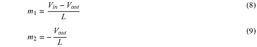
[0055] The principles of the predictive buck average input current control loop are similar to those of the boost current control loop. For the buck converter, the on-time and off-time inductor slopes are given by the following equations:
m 1 = V i n - V out L ( 8 ) m 2 = - V out L ( 9 ) ##EQU00007##
[0056] For switching cycle number n the average input current, based on the inductor current, is:
i ~ ( n ) = ( i ( n - 1 ) + m 1 d [ n ] Ts L + m 2 d ' [ n ] Ts L ) * d [ n ] ( 10 ) ##EQU00008##
[0057] Based on equations (8) and (9) we can predict the inductor current for one switching cycle, and get the following equation:
i ( n ) = i ( n - 1 ) + ( V i n - V out ) d [ n ] T s L - V out d ' [ n ] T s L ( 11 ) ##EQU00009##
[0058] Combining equations (10) and (11) we get:
i ~ ( n + 1 ) = ( i ( n - 1 ) + V in d [ n ] Ts L - 2 V out Ts L + V in d [ n + 1 ] T s L ) d [ n + 1 ] ( 12 ) ##EQU00010##
[0059] The prediction for the duty cycle d[n +1] can now be obtained based on the values sampled in the previous switching period. Denoting the sampled current as i.sub.s[n], and substituting the control objective (n+1)=I.sub.ref in (11), we have:
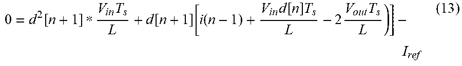
0 = d 2 [ n + 1 ] * V in T s L + d [ n + 1 ] [ i ( n - 1 ) + V in d [ n ] T s L - 2 V out T s L ) ] - I ref ( 13 ) ##EQU00011##
[0060] Equation (13) is the control law when the converter is in buck mode. Because of the fact that this equation is a quadratic equation, one of the methods of solving it in an efficient manner is to use Newton Raphson method to approximate the solution.
[0061] If we denote T.sub.i as the beginning time of each switching cycle (i), the above method samples the input voltage, output voltage, and inductor current at time T.sub.0, utilizes the time until T.sub.1 to predict the inductor current at T.sub.1 using the input voltage, output voltage and the knowledge of the inductor inductance, and calculate the needed duty-cycle in order to reach the desired input current (I.sub.ref) at T.sub.2, that is dependent on the inductor current and the duty cycle at T.sub.2, and set that duty cycle to be performed in the switching cycle between T.sub.1 and T.sub.2.
[0062] Predictive Buck Input Current Control--Alternative Embodiment
[0063] Another method for controlling the converter's input current in a buck converting is by controlling the inductor current and using the converter's input and output voltage to set the correct inductor reference value in an adaptive manner. FIG. 5 shows the block diagram of the control loops for this method. Equation 14 holds true in steady state in a buck converter:
I ~ in = V out V in I ~ L ( 14 ) ##EQU00012##
[0064] By using equation (14) we can set the required inductor current (I.sub.L_Ref) according to V.sub.in and V.sub.out in the following way:
I L_Ref = I ref * V in V out ( 15 ) ##EQU00013##
[0065] Equation (15) is the feed-forward block that runs every switching cycle. After calculating the cycle-by-cycle inductor current reference, an inductor current loop is used to set the required inductor current.
[0066] Predictive Buck Inductor Current Control
[0067] By using equation (11), extending it for two switching cycles and replacing i(n) with i.sub.pred(n) we get the following equation:
i ( n + 1 ) = i pred ( n ) + V in d [ n + 1 ] T s L - V out T s L ( 16 ) ##EQU00014##
[0068] By solving equation (16) for d[n+1] we get:
d [ n + 1 ] = ( I L_ref - I pred [ n ] ) L T s * V in + V out V in ( 17 ) ##EQU00015##
[0069] Because of the fact that the inductor inductance can vary and to be able to achieve a slower control loop, we modify equation (17) with a variable gain that can be pre-adjusted, and we get:
d [ n + 1 ] = ( I L_ref - I pred [ n ] ) L * K T s * V in + V out V in ( 18 ) ##EQU00016##
[0070] Equation (18) is the control law for the buck inductor current loop.
[0071] If we denote T.sub.i as the beginning time of each switching cycle (i), the above method samples the input voltage, output voltage, and inductor current at time T.sub.0, utilizes the time until T.sub.1 to estimate the needed inductor current (I.sub.L_Ref) according to the input voltage, output voltage and desired input current (I.sub.ref). In addition, predicting the inductor current at T.sub.1 using the input voltage, output voltage and the knowledge of the inductor inductance, and calculate the needed duty-cycle in order to reach the needed inductor current (I.sub.L_ref) at T.sub.2, and set that duty cycle to be performed in the switching cycle between T.sub.1 and T.sub.2.
[0072] Predictive Cascaded Buck-Boost Input Current Control
[0073] When the converter is in buck-boost mode all four switches are being used to set the correct converter's average input current. This can be shown in FIG. 6 for trailing triangle PWM modulation. Switches B and D are complementary to switches A and C respectively. In each switching cycle both the buck and boost switches are being used to control the converter's average input current. In general, the boost switches will operate at a low duty cycle while the buck switches will operate at a high duty cycle.
[0074] FIG. 6 illustrates a method enabling the converter to set the converter's average input current correctly when the output current is relatively close to the reference current. In order to simplify the control loop the buck duty cycle will be fixed to a value, d.sub.buck, and the control loop will set the boost duty cycle every switching cycle.
[0075] FIG. 7 illustrates the inductor current waveforms for a buck-boost switching cycle. The on-time and off-time inductor current slopes for the buck cycle and boost cycle are identical to the equations in (8), (9) and (1), (2). In addition, the average input current can be calculated from the average inductor current with the following equation:
.sub.In= .sub.L*d.sub.buck (19)
[0076] Based on all these equations the predictive control law can be built for calculating the required boost duty cycle:
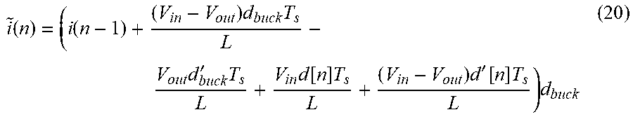
i ~ ( n ) = ( i ( n - 1 ) + ( V in - V out ) d buck T s L - V out d buck ' T s L + V in d [ n ] T s L + ( V in - V out ) d ' [ n ] T s L ) d buck ( 20 ) ##EQU00017##
[0077] Denoting the sampled current as i.sub.s[n] substituting the control objective (n)=i.sub.ref in the equation above, and solving for d[n], we get the following:
d [ n ] = 2 + ( i ref d buck - i s [ n ] ) L V out T s - V in V out d buck ( 21 ) ##EQU00018##
[0078] Equation (21) is the control law for setting the boost duty cycle when the converter is in buck-boost mode.
[0079] If we denote T.sub.i as the beginning time of each switching cycle (i), the above method samples the input voltage, output voltage, and inductor current at time T.sub.0, utilizes the time until T.sub.1 to predict the inductor current at T.sub.1, based on the fact that the converter is in alternating buck-boost mode, using the input voltage, output voltage and the knowledge of the inductor inductance, and calculate the needed duty-cycle in order to reach the desired input current (I.sub.ref) at T.sub.2, and set that duty cycle to be performed in the switching cycle between T.sub.1 and T.sub.2.
[0080] Predictive Buck-Boost Input Current Control--Alternative Embodiment
[0081] Another method for controlling the converter's input current in a cascaded buck-boost converting is by controlling the inductor current and using the input and output voltage to set the correct inductor reference value in an adaptive manner. FIG. 8 shows the block diagram of the control loops for this method.
[0082] Predictive Buck-Boost Inductor Current Control
[0083] An efficient method of controlling the inductor current in a cascaded buck-boost converter is setting a linear relation between the boost and buck duty cycle in the following manner:
d.sub.buck=1-c+d.sub.boost (22)
[0084] Where:
0.ltoreq.c.ltoreq.1
[0085] Using equations (1), (2), (8) and (9) we can estimate the inductor at the end of switching cycle n:
i ( n ) = i ( n - 1 ) + ( V in - V out ) d buck [ n ] T s L - V out d buck ' [ n ] T s L + V in d boost [ n ] T s L + ( V in - V out ) d boost ' [ n ] T s L i ( n ) = i ( n - 1 ) + V in d buck [ n ] T s L + V in d boost [ n ] T s L + ( V in - 2 V out ) Ts L ( 23 ) ##EQU00019##
[0086] Combining equations (22) and (23) and we get:
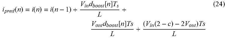
i pred ( n ) = i ( n ) = i ( n - 1 ) + V in d boost [ n ] T s L + V out d boost [ n ] Ts L + ( V in ( 2 - c ) - 2 V out ) Ts L ( 24 ) ##EQU00020##
[0087] By extending equation (24) to another switching cycle we get:
i ( n + 1 ) = i pred ( n ) + V in d boost [ n ] T s L + V out d boost [ n + 1 ] Ts L + ( V in ( 2 - c ) - 2 V out ) Ts L ( 25 ) ##EQU00021##
[0088] Solving equation (25) for d.sub.boost[n+1] and replacing i(n+1) with the control objective, I.sub.L_Ref, we get:
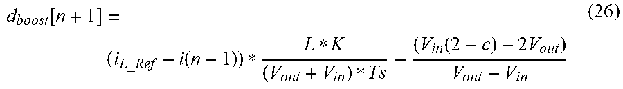
d boost [ n + 1 ] = ( i L_Ref - i ( n - 1 ) ) * L * K ( V out + V in ) * Ts - ( V in ( 2 - c ) - 2 V out ) V out + V in ( 26 ) ##EQU00022##
[0089] Equation (26) is the control law for the inductor current control in a cascaded buck-boost converter.
[0090] Feed Forward
[0091] In order to control the converter's input current, a cycle by cycle feed-forward is used in order to change the inductor current reference according to the required converter input current and input and output voltage. In a cascaded buck-boost converter we know that in steady state:
V out V in = D buck 1 - D boost ( 27 a ) i ~ in i ~ l = D buck ( 27 b ) ##EQU00023##
[0092] Using equations (27) and (22) we can get:
i L_Ref = i ref V in + V out ( 2 - c ) V out ( 28 ) ##EQU00024##
[0093] Using equation (28) we can set the required inductor current according to the desired input current and input and output voltages.
[0094] If we denote T.sub.i as the beginning time of each switching cycle (i), the above method samples the input voltage, output voltage, and inductor current at time T.sub.0, utilizes the time until T.sub.1 to estimate the needed inductor current (I.sub.L_Ref) according to the input voltage, output voltage and desired input current (I.sub.ref). In addition, predicting the inductor current at T.sub.1 using the input voltage, output voltage and the knowledge of the inductor inductance, and calculate the needed duty-cycle in order to reach the needed inductor current (I.sub.L_ref) at T.sub.2, and set that duty cycle to be performed in the switching cycle between T.sub.1 and T.sub.2.
[0095] Switching Between Converter Modes
[0096] The converter needs to switch between three different modes depending on the reference current and the output current. FIG. 9 shows a state diagram and the possible options to switch between the three different states. The following sections will describe the logic from switching between the different states.
[0097] Switching From Buck Mode
[0098] When in buck mode, the duty cycle will be monitored every switching cycle. If the duty cycle is higher than the threshold set, 0<Th.sub.bucl<1, for more than X.sub.buck consecutive switching cycles the converter will switch to buck-boost mode.
[0099] Switching From Buck-Boost Mode
[0100] When in buck-boost mode, the duty cycle of the boost converter will be monitored every boost switching cycle (every second switching cycle). Two thresholds will be set--Th.sub.high and Th.sub.low. If the duty cycle is higher than Th.sub.high for more than X.sub.high consecutive switching cycles the converter will switch to boost mode. If the duty cycle is lower than Th.sub.low for more than X.sub.low consecutive switching cycles the converter will switch to buck mode.
[0101] Switching From Boost Mode
[0102] When in boot mode, the duty cycle will be monitored every switching cycle. If the duty cycle is lower than the threshold set, 0<Th.sub.boost<1, for more than X.sub.boost consecutive switching cycles the converter will switch to buck-boost mode.
* * * * *
D00000
D00001
D00002
D00003
D00004


XML
uspto.report is an independent third-party trademark research tool that is not affiliated, endorsed, or sponsored by the United States Patent and Trademark Office (USPTO) or any other governmental organization. The information provided by uspto.report is based on publicly available data at the time of writing and is intended for informational purposes only.
While we strive to provide accurate and up-to-date information, we do not guarantee the accuracy, completeness, reliability, or suitability of the information displayed on this site. The use of this site is at your own risk. Any reliance you place on such information is therefore strictly at your own risk.
All official trademark data, including owner information, should be verified by visiting the official USPTO website at www.uspto.gov. This site is not intended to replace professional legal advice and should not be used as a substitute for consulting with a legal professional who is knowledgeable about trademark law.