Vehicular Sensing Device With Cooling Feature
Wohlte; Wilhelm Johann Wolfgang
U.S. patent application number 16/662205 was filed with the patent office on 2020-04-30 for vehicular sensing device with cooling feature. The applicant listed for this patent is Magna Electronics Inc.. Invention is credited to Wilhelm Johann Wolfgang Wohlte.
| Application Number | 20200137926 16/662205 |
| Document ID | / |
| Family ID | 70325723 |
| Filed Date | 2020-04-30 |


| United States Patent Application | 20200137926 |
| Kind Code | A1 |
| Wohlte; Wilhelm Johann Wolfgang | April 30, 2020 |
VEHICULAR SENSING DEVICE WITH COOLING FEATURE
Abstract
A sensing device for a vehicular sensing system includes a housing having a front housing portion and a metallic rear housing portion. A first printed circuit board and a second printed circuit board are disposed in the housing. The second printed circuit board is electrically connected to the first printed circuit board, which has an electrical connector for electrically connecting the sensing device to a vehicle wire harness. The second printed circuit board has circuitry thereat, with the circuitry generating heat when the sensing device is operating. The rear housing portion comprises a thermally conductive element that extends through an aperture of the first printed circuit board and is thermally coupled at the second printed circuit board. The thermally conductive element conducts heat generated by the circuitry of the second printed circuit board to the rear housing portion to dissipate the heat from the sensing device.
| Inventors: | Wohlte; Wilhelm Johann Wolfgang; (Sailauf, DE) | ||||||||||
| Applicant: |
|
||||||||||
|---|---|---|---|---|---|---|---|---|---|---|---|
| Family ID: | 70325723 | ||||||||||
| Appl. No.: | 16/662205 | ||||||||||
| Filed: | October 24, 2019 |
Related U.S. Patent Documents
| Application Number | Filing Date | Patent Number | ||
|---|---|---|---|---|
| 62750894 | Oct 26, 2018 | |||
| Current U.S. Class: | 1/1 |
| Current CPC Class: | H05K 7/20436 20130101; G01S 2007/027 20130101; H05K 7/205 20130101; H05K 7/20854 20130101; H05K 1/144 20130101; H05K 2201/09063 20130101; H05K 1/0284 20130101; G01S 7/03 20130101; H05K 2201/10189 20130101; H05K 7/20518 20130101; G01S 7/4813 20130101; H01L 23/40 20130101 |
| International Class: | H05K 7/20 20060101 H05K007/20; H01L 23/40 20060101 H01L023/40; H05K 1/02 20060101 H05K001/02; H05K 1/14 20060101 H05K001/14; G01S 7/03 20060101 G01S007/03; G01S 7/481 20060101 G01S007/481 |
Claims
1. A radar device for a vehicular sensing system, said radar device comprising: a housing having a front housing portion and a metallic rear housing portion, wherein said front housing portion and said metallic rear housing portion are joined together to establish a cavity; a first printed circuit board and a second printed circuit board disposed in the cavity of said housing, wherein said second printed circuit board is electrically connected to said first printed circuit board; wherein said first printed circuit board has an electrical connector for electrically connecting said radar device to a wire harness of a vehicle when said radar device is disposed at the vehicle, and wherein said first printed circuit board has an aperture therethrough; wherein said second printed circuit board has circuitry disposed thereat, and wherein the circuitry generates heat when said radar device is operating; wherein said metallic rear housing portion has a thermally conductive element extending into the cavity from a rear wall of said metallic rear housing portion; wherein said thermally conductive element extends through said aperture of said first printed circuit board and is thermally coupled at said second printed circuit board; and wherein said thermally conductive element conducts heat generated by the circuitry of said second printed circuit board to said rear wall of said metallic rear housing portion to dissipate the heat from said radar device.
2. The radar device of claim 1, wherein the circuitry that generates heat when said radar device is operating comprises a data processor chip.
3. The radar device of claim 2, wherein said thermally conductive element thermally couples to the data processor chip of said second printed circuit board.
4. The radar device of claim 1, wherein the circuitry comprises a radar sensor comprising transmitting antennas and receiving antennas.
5. The radar device of claim 1, wherein the aperture through said first printed circuit board comprises a cutout through said first printed circuit board with said first printed circuit board partially circumscribing the cutout.
6. The radar device of claim 5, wherein the cutout comprises a notch extending inboard from a peripheral region of said first printed circuit board.
7. The radar device of claim 1, wherein the aperture through said first printed circuit board comprises a cutout through said first printed circuit board with said first printed circuit board fully circumscribing the cutout.
8. The radar device of claim 7, wherein the cutout comprises a hole inboard of a periphery of said first printed circuit board.
9. The radar device of claim 1, wherein said thermally conductive element is thermally coupled at said second printed circuit board via a thermally conductive material.
10. The radar device of claim 9, wherein the thermally conductive material comprises a thermally conductive pliable material.
11. The radar device of claim 9, wherein the thermally conductive material comprises a thermally conductive paste.
12. The radar device of claim 1, wherein said thermally conductive element comprises a cylindrically-shaped element.
13. The radar device of claim 1, wherein said thermally conductive element comprises a rectangular-shaped element.
14. The radar device of claim 1, wherein said thermally conductive element comprises a conically-shaped element.
15. The radar device of claim 1, wherein said thermally conductive element comprises a metallic thermally conductive element.
16. The radar device of claim 15, wherein said thermally conductive element is formed as an integral part of said metallic rear housing portion.
17. The radar device of claim 1, wherein said metallic rear housing portion comprises a plurality of heat dissipating elements protruding from an outermost surface of said rear wall to enhance heat dissipation at said rear wall of said metallic rear housing portion.
18. The radar device of claim 1, wherein said metallic rear housing portion is formed of at least one selected from the group consisting of zinc, aluminum and magnesium.
19. A lidar device for a vehicular sensing system, said lidar device comprising: a housing having a front housing portion and a metallic rear housing portion, wherein said front housing portion and said metallic rear housing portion are joined together to establish a cavity; a first printed circuit board and a second printed circuit board disposed in the cavity of said housing, wherein said second printed circuit board is electrically connected to said first printed circuit board; wherein said first printed circuit board has an electrical connector for electrically connecting said lidar device to a wire harness of a vehicle when said lidar device is disposed at the vehicle, and wherein said first printed circuit board has an aperture therethrough, the aperture comprising a cutout through said first printed circuit board with said first printed circuit board at least partially circumscribing the cutout; wherein said second printed circuit board has circuitry disposed thereat, and wherein the circuitry generates heat when said lidar device is operating; wherein the circuitry that generates heat when said lidar device is operating comprises a data processor chip; wherein said metallic rear housing portion has a metallic thermally conductive element extending into the cavity from a rear wall of said metallic rear housing portion; wherein said metallic thermally conductive element extends through said aperture of said first printed circuit board and is thermally coupled at said second printed circuit board; and wherein said metallic thermally conductive element conducts heat generated by the circuitry of said second printed circuit board to said rear wall of said metallic rear housing portion to dissipate the heat from said lidar device.
20. The lidar device of claim 19, wherein said metallic thermally conductive element is thermally coupled at said second printed circuit board via a thermally conductive paste.
21. The lidar device of claim 19, wherein said metallic thermally conductive element is formed as an integral part of said metallic rear housing portion.
22. The lidar device of claim 19, wherein said metallic rear housing portion comprises a plurality of heat dissipating elements protruding from an outermost surface of said rear wall to enhance heat dissipation at said rear wall of said metallic rear housing portion.
23. The lidar device of claim 19, wherein said metallic thermally conductive element thermally couples to the data processor chip of said second printed circuit board.
24. A radar device for a vehicular sensing system, said radar device comprising: a housing having a front housing portion and a metallic rear housing portion, wherein said front housing portion and said metallic rear housing portion are joined together to establish a cavity; a first printed circuit board and a second printed circuit board disposed in the cavity of said housing, wherein said second printed circuit board is electrically connected to said first printed circuit board; wherein said first printed circuit board has an electrical connector for electrically connecting said radar device to a wire harness of a vehicle when said radar device is disposed at the vehicle, and wherein said first printed circuit board has an aperture therethrough, the aperture comprising a cutout at said first printed circuit board with said first printed circuit board at least partially circumscribing the cutout; wherein said second printed circuit board has circuitry disposed thereat, and wherein the circuitry generates heat when said radar device is operating; wherein the circuitry that generates heat when said radar device is operating comprises a data processor chip; wherein said metallic rear housing portion has a metallic thermally conductive element extending into the cavity from a rear wall of said metallic rear housing portion; wherein said metallic thermally conductive element extends through said aperture of said first printed circuit board and is thermally coupled at said second printed circuit board; wherein said metallic thermally conductive element conducts heat generated by the circuitry of said second printed circuit board to said rear wall of said metallic rear housing portion to dissipate the heat from said radar device; and wherein said metallic rear housing portion comprises a plurality of heat dissipating elements protruding from an outermost surface of said rear wall to enhance heat dissipation at said rear wall of said metallic rear housing portion.
25. The radar device of claim 24, wherein said metallic thermally conductive element thermally couples to the data processor chip of said second printed circuit board.
26. The radar device of claim 24, wherein said metallic thermally conductive element is thermally coupled at said second printed circuit board via a thermally conductive material.
27. The radar device of claim 24, wherein said metallic thermally conductive element is formed as an integral part of said metallic rear housing portion.
Description
CROSS REFERENCE TO RELATED APPLICATION
[0001] The present application claims the filing benefits of U.S. provisional application Ser. No. 62/750,894, filed Oct. 26, 2018, which is hereby incorporated herein by reference in its entirety.
FIELD OF THE INVENTION
[0002] The present invention relates generally to a vehicle sensing system for a vehicle and, more particularly, to a vehicle sensing system that utilizes one or more radar sensors and/or cameras at a vehicle.
BACKGROUND OF THE INVENTION
[0003] Use of imaging and radar sensors in vehicle sensing systems is common and known. Examples of such known systems are described in U.S. Pat. No. 8,013,780, which is hereby incorporated herein by reference in its entirety.
SUMMARY OF THE INVENTION
[0004] The present invention provides a driving assistance system or sensing system or vehicle control system for a vehicle that utilizes one or more sensors, such as radar sensors or image sensors or lidar sensors, to sense regions exterior of the vehicle. The sensor includes a thermal element that is thermally coupled at a circuit board of the sensor (that has an integrated circuit or processor thereat) to draw heat (that is generated by operation of the sensor) away from the circuit board and to a distal rear housing portion of the sensor. The thermal element may be part of the rear housing portion and both may comprise metallic thermally conductive materials.
[0005] These and other objects, advantages, purposes and features of the present invention will become apparent upon review of the following specification in conjunction with the drawings.
BRIEF DESCRIPTION OF THE DRAWINGS
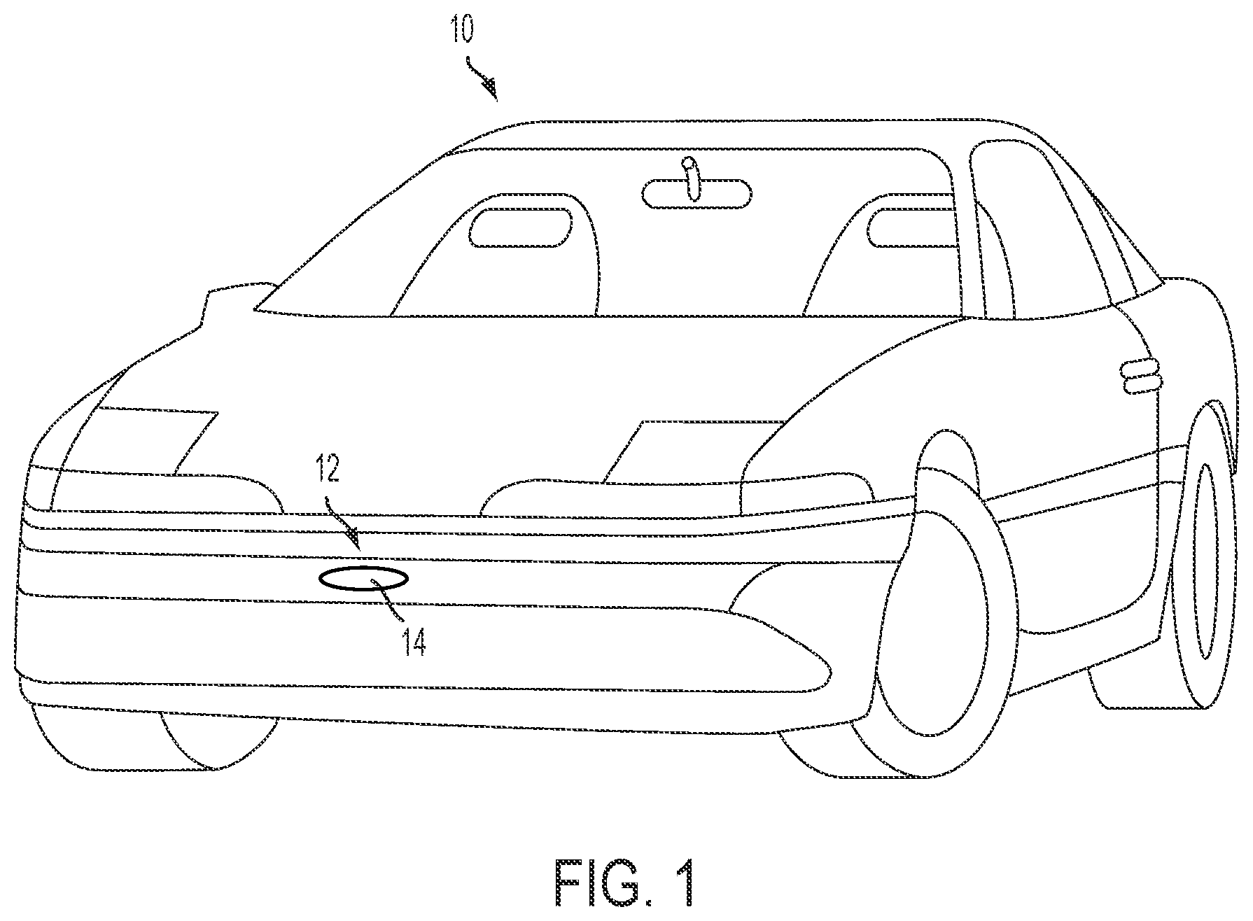
[0006] FIG. 1 is a perspective view of a vehicle with a sensing system that incorporates a radar sensor in accordance with the present invention;
[0007] FIG. 2 is a sectional view of the radar sensor;
[0008] FIG. 3 is an enlarged view of the thermal element, showing the heat transfer from the circuit board to the rear housing of the sensor;
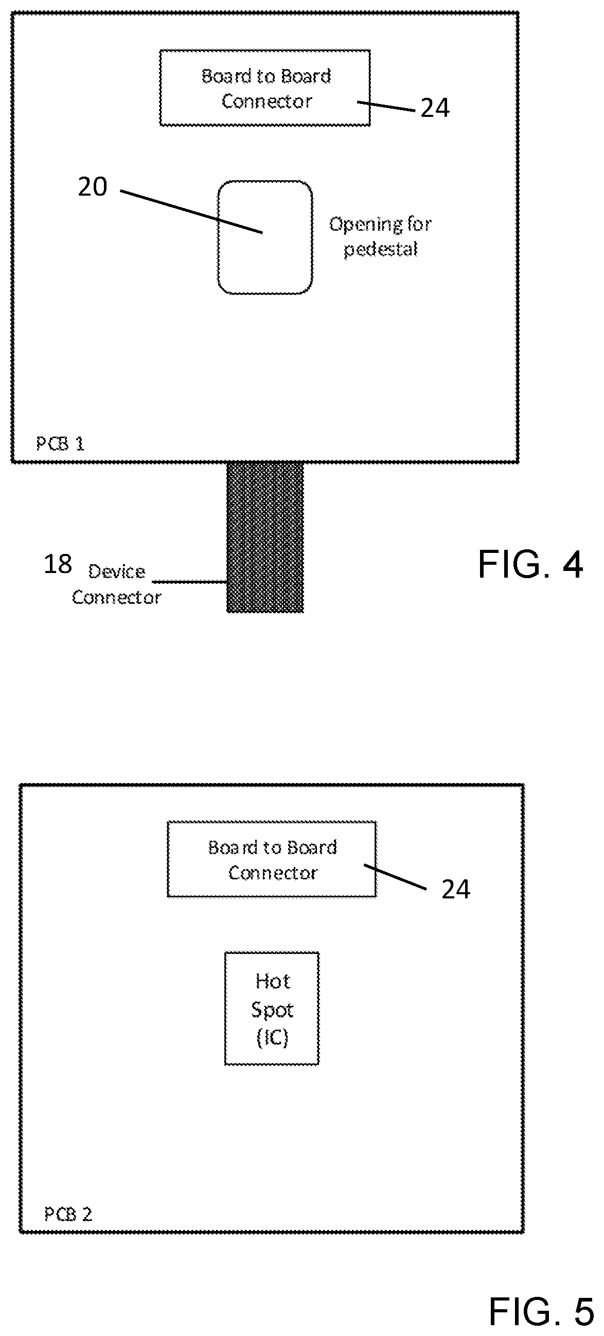
[0009] FIG. 4 is a plan view of the connector circuit board, showing the aperture or opening for the thermal element to pass through; and
[0010] FIG. 5 is a plan view of the second circuit board, showing the IC disposed thereat.
DESCRIPTION OF THE PREFERRED EMBODIMENTS
[0011] A vehicle sensing system and/or driver assist system and/or driving assist system and/or object detection system and/or alert system operates to capture sensing data exterior of the vehicle and may process the captured data to detect objects at or near the vehicle and in the predicted path of the vehicle, such as to assist a driver of the vehicle or a control for an autonomous vehicle in maneuvering the vehicle in a forward or rearward direction. The system includes a processor that is operable to receive sensing data from one or more sensors and provide an output, such as an alert or control of a vehicle system.
[0012] Referring now to the drawings and the illustrative embodiments depicted therein, a vehicle 10 (FIG. 1) includes an driving assistance system or sensing system 12 that includes at least one radar sensor unit, such as a forward facing radar sensor unit 14 (and the system may optionally include multiple exterior facing sensors, such as cameras or other sensors, such as a rearward facing sensor at the rear of the vehicle, and a sideward/rearward facing sensor at respective sides of the vehicle), which senses regions exterior of the vehicle. The sensing system 12 includes a control or electronic control unit (ECU) or processor that is operable to process data captured by the sensor or sensors and may detect objects or the like. The data transfer or signal communication from the sensor to the ECU may comprise any suitable data or communication link, such as a vehicle network bus or the like of the equipped vehicle.
[0013] The radar sensor or sensors of the driving assist system may be used in conjunction with a plurality of image sensors mounted at the equipped vehicle and/or with at least one lidar sensor also mounted (along with the image sensors and the radar sensor) at the equipped vehicle. Image data and/or radar data and/or lidar data may be provided to a central electronic control unit (ECU) or module for processing thereat. The ECU includes at least one processor that processes the captured/sensed data, whereby one or more functions or systems (such as a braking system and/or steering system and/or the like) of the vehicle is controlled responsive to processing of the captured/sensed data.
[0014] Modern ADAS applications such as RADAR, LIDAR or cameras are built on high-performance integrated circuits (ICs). Such ICs can generate heat which needs to be transferred out of the sensor and housing to ensure compliance requirements. Quite often such vehicular sensing systems are built with multiple PCBs. In some cases, the hot-spot is located on the PCB which is not directly adjacent to the rear housing, which can be out of metal and used as heat sink.
[0015] The radar sensor of the vehicular sensing system includes a plurality of transmitter antennas and a plurality of receiver antennas, which may be disposed on a printed circuit board (PCB) that includes associated circuitry. The sensor includes a thermally conductive element that extends or protrudes from (or is part of) the rear housing (e.g., a metallic rear housing) and that contacts and is thermally coupled with the rear of a printed circuit board that has circuitry disposed thereat that generates heat during operation of the sensor.
[0016] As shown in FIG. 2, a radar sensor 16 has two printed circuit boards (PCB1 and PCB2), with one printed circuit board (PCB1) having a connector 18 for electrically connecting the sensor to a wire or lead of the vehicle and having an aperture or cutout 20 therethrough for the thermal element or pedestal 22 to pass. The other printed circuit board (PCB2) has a processor and/or integrated circuit (IC) or processor or processing chip that generates heat when operating. The PCB2 is electrically connected to PCB1 via an electrical connector 24 (such as a flexible ribbon cable connector or other suitable connector that electrically connects circuitry of PCB2 to circuitry of PCB1). The front housing portion 26 (e.g., a plastic housing portion) may be adhesively attached or mated or joined or may be welded or fastened (such as via one or more fasteners) to the rear housing portion 28 (e.g., a metallic housing portion comprising, for example, aluminum, zinc, magnesium or the like or alloys thereof), and optionally with a gasket or sealing element to seal the housing with a cavity defined or formed therein. Also, the PCB1 and PCB2 may be attached at the front or rear housing portion via any suitable means, such as adhesive or fasteners or the like. For example, the printed circuit board PCB1 may be fastened at the rear housing (such as to the rear wall of the rear housing) while the other printed circuit board PCB2 may be attached at the front housing portion.
[0017] In the illustrated embodiment, the thermally conductive pedestal 22 extends from the inner surface of the rear housing 28 (and may be formed as part of the rear housing or may be thermally coupled with the rear housing). The distal end of the thermally conductive pedestal (that is distal from the rear wall of the rear housing) is thermally coupled at PCB2 and at the circuitry where the most heat is generated during operation of the sensor. The distal end of the thermally conductive pedestal may be coupled to the printed circuit board PCB2 via a thermally conductive material. The thermally conductive material that thermally couples the pedestal to the rear side of the printed circuit board PCB2 (or to a component or circuitry disposed at the printed circuit board, such as at the rear side of the printed circuit board) may comprise a thermally conductive pliable material or a thermally conductive paste or other suitable material that enhances contact and thermal conductivity between the printed circuit board PCB2 and the thermally conductive pedestal.
[0018] During operation of the sensor, heat generated at the circuitry on PCB2 is transferred from PCB2 through the thermal coupling material and along the thermally conductive pedestal to the rear wall of the rear housing. Optionally, the rear housing may include a heat sink at the rear wall of the rear housing (such as a plurality of heat dissipating fins or vanes or protruding elements formed at the exterior or outermost surface of the rear wall of the rear housing) to enhance heat dissipation from the thermal coupler at the rear housing of the sensor.
[0019] Thus, the PCB(s) of the sensor that is/are between the hot spot(s) (e.g., at one or more ICs at PCB2) and the potential heat sink (at the rear wall of the housing) may have a cut out or aperture therethrough, with the aperture being bounded or defined by a portion of the PCB substrate that at least partially circumscribes the cutout and the thermally conductive pedestal passing therethrough. For example, the aperture may comprise a cutout or hole (as shown in FIG. 4) drilled or otherwise established through a central or non-peripheral or non-perimeter region of the PCB substrate of PCB1 so that the PCB substrate fully circumscribes the aperture and the thermally conductive pedestal that passes therethrough. Optionally, the aperture may comprise a notch or cutout that extends from or that is adjacent to or at a perimeter or peripheral region of the PCB substrate such that the PCB substrate partially circumscribes the cutout and the thermally conductive pedestal that passes through the cutout. The thermally conductive pedestal passes through the aperture and is thermally coupled to the IC/circuitry (such as via application of a thermal grease or a thermal pad or the like). The generated heat is spread out through the thermal coupling of the IC to the metal pedestal, which may be part of the rear housing. The rear housing can be mounted directly on a metallic part of the car or can be placed in a metallic bracket, such that the heat generated during operation of the sensor is transferred from the IC to the environment.
[0020] Although shown and described as being part of a radar sensor, the thermally conductive pedestal may be used for other sensors and/or processors of an automotive driving assistance system or the like. For example, the thermally conductive pedestal may be implemented in a radar sensor, a lidar sensor, a camera, a data processor or processing ECU and/or other sensors and/or processors of the ADAS. FIGS. 2-5 show a radar sensor application. For camera applications, the front housing would include a lens holder and lens, while for LiDAR applications, it would be a front housing (with or without a heating structure) similar to what is shown in FIGS. 2-5. Although the sensor is shown with two PCBs, the sensor may have three PCBs or more, with the thermally conductive pedestal protruding through more than one PCB (each having an aperture formed therethrough to accommodate the pedestal). The shape of the pedestal (i.e., the shape of a cross section of the pedestal taken along a plane that is normal to the longitudinal axis of the pedestal) may be any suitable shape, such as a square shape or a rectangular shape or a circular shape (such as for a pedestal having a cylindrical shape or a conical shape), to enhance or optimize or maximize the amount of metal that is used to transfer the heat out the sensor or device. The shape of the aperture 20 may be selected to correspond with the shape of the pedestal, such as, for example, a rectangular shape as shown in FIG. 4 for a rectangular cross section pedestal, or such as via a circular or oval shape or the like for a cylindrical shaped or conical shaped pedestal.
[0021] Although shown as a single pedestal extending from a generally central region of the rear housing and through a generally central region of the PCB1, the pedestal may be elsewhere positioned at the rear wall of the rear housing and may extend through an aperture or cutout correspondingly formed or established through the PCB1. Optionally, two or more pedestals may be provided to thermally couple at two or more components or circuitry elements of the PCB2. Optionally, the one or more pedestals may be formed to provide a locating element or support structure for locating and/or supporting the PCB1 at a desired location in the cavity. For example, the pedestal(s) may have a stepped shape (or a conical shape) with a larger cross dimension closer to the rear wall of the rear housing so that the PCB1 can engage the step (or larger diameter portion) and be located and/or supported at the pedestal(s). The PCB1 may be fastened or secured at the desired or selected location, such as via one or more fasteners or the like attaching the PCB1 to the pedestal or to the rear housing. For applications where there are three or more PCBs, the pedestal(s) may have multiple stepped structure to accommodate and locate the two or more PCBs having an aperture therethrough (and the PCBs may have different sized apertures to engage the different diameter portions of the pedestal or pedestals).
[0022] The sensor or sensing system may utilize aspects of the systems described in U.S. Pat. Nos. 9,753,121; 9,689,967; 9,599,702; 9,575,160; 9,146,898; 9,036,026; 8,027,029; 8,013,780; 6,825,455; 7,053,357; 7,408,627; 7,405,812; 7,379,163; 7,379,100; 7,375,803; 7,352,454; 7,340,077; 7,321,111; 7,310,431; 7,283,213; 7,212,663; 7,203,356; 7,176,438; 7,157,685; 6,919,549; 6,906,793; 6,876,775; 6,710,770; 6,690,354; 6,678,039; 6,674,895 and/or 6,587,186, and/or International Publication Nos. WO 2018/007995 and/or WO 2011/090484, and/or U.S. Publication Nos. US-2018-0231635; US-2018-0045812; US-2018-0015875; US-2017-0356994; US-2017-0315231; US-2017-0276788; US-2017-0254873; US-2017-0222311 and/or US-2010-0245066, which are hereby incorporated herein by reference in their entireties.
[0023] Optionally, the sensor (such as an image sensor or camera) or sensing system may utilize aspects of the cameras and systems described in U.S. Pat. Nos. 9,621,769; 9,596,387; 9,277,104; 9,077,098; 8,994,878; 8,542,451 and/or 7,965,336, and/or U.S. Publication Nos. US-2009-0244361; US-2013-0242099; US-2014-0373345; US-2015-0124098; US-2015-0222795; US-2015-0327398; US-2016-0243987; US-2016-0268716; US-2016-0286103; US-2016-0037028; US-2017-0054881; US-2017-0133811; US-2017-0201661; US-2017-0280034; US-2017-0295306; US-2017-0302829; US-2018-0098033; US-2019-0124238; US-2019-0124243; US-2019-0121051 and/or US-2019-0306966, and/or U.S. patent applications, Ser. No. 16/451,179, filed Jun. 25, 2019 (Attorney Docket MAGO4 P3623), and/or Ser. No. 16/525,666, filed Jul. 30, 2019 (Attorney Docket MAGO4 P3643), which are all hereby incorporated herein by reference in their entireties.
[0024] The system includes an image processor operable to process image data captured by the camera or cameras, such as for detecting objects or other vehicles or pedestrians or the like in the field of view of one or more of the cameras. For example, the image processor may comprise an image processing chip selected from the EYEQ.TM. family of image processing chips (for example, an EYEQ3.TM., EYEQ4.TM. or EYEQ5.TM. image processing chip) available from Mobileye Vision Technologies Ltd. of Jerusalem, Israel, and may include object detection software (such as the types described in U.S. Pat. Nos. 7,855,755; 7,720,580 and/or 7,038,577, which are hereby incorporated herein by reference in their entireties), and may analyze image data to detect vehicles and/or other objects. Responsive to such image processing, and when an object or other vehicle is detected, the system may generate an alert to the driver of the vehicle and/or may generate an overlay at the displayed image to highlight or enhance display of the detected object or vehicle, in order to enhance the driver's awareness of the detected object or vehicle or hazardous condition during a driving maneuver of the equipped vehicle.
[0025] For example, the vision system and/or processing and/or camera and/or circuitry may utilize aspects described in U.S. Pat. Nos. 9,233,641; 9,146,898; 9,174,574; 9,090,234; 9,077,098; 8,818,042; 8,886,401; 9,077,962; 9,068,390; 9,140,789; 9,092,986; 9,205,776; 8,917,169; 8,694,224; 7,005,974; 5,760,962; 5,877,897; 5,796,094; 5,949,331; 6,222,447; 6,302,545; 6,396,397; 6,498,620; 6,523,964; 6,611,202; 6,201,642; 6,690,268; 6,717,610; 6,757,109; 6,802,617; 6,806,452; 6,822,563; 6,891,563; 6,946,978; 7,859,565; 5,550,677; 5,670,935; 6,636,258; 7,145,519; 7,161,616; 7,230,640; 7,248,283; 7,295,229; 7,301,466; 7,592,928; 7,881,496; 7,720,580; 7,038,577; 6,882,287; 5,929,786 and/or 5,786,772, and/or U.S. Publication Nos. US-2014-0340510; US-2014-0313339; US-2014-0347486; US-2014-0320658; US-2014-0336876; US-2014-0307095; US-2014-0327774; US-2014-0327772; US-2014-0320636; US-2014-0293057; US-2014-0309884; US-2014-0226012; US-2014-0293042; US-2014-0218535; US-2014-0218535; US-2014-0247354; US-2014-0247355; US-2014-0247352; US-2014-0232869; US-2014-0211009; US-2014-0160276; US-2014-0168437; US-2014-0168415; US-2014-0160291; US-2014-0152825; US-2014-0139676; US-2014-0138140; US-2014-0104426; US-2014-0098229; US-2014-0085472; US-2014-0067206; US-2014-0049646; US-2014-0052340; US-2014-0025240; US-2014-0028852; US-2014-005907; US-2013-0314503; US-2013-0298866; US-2013-0222593; US-2013-0300869; US-2013-0278769; US-2013-0258077; US-2013-0258077; US-2013-0242099; US-2013-0215271; US-2013-0141578 and/or US-2013-0002873, which are all hereby incorporated herein by reference in their entireties. The system may communicate with other communication systems via any suitable means, such as by utilizing aspects of the systems described in International Publication Nos. WO/2010/144900; WO 2013/043661 and/or WO 2013/081985, and/or U.S. Pat. No. 9,126,525, which are hereby incorporated herein by reference in their entireties.
[0026] Changes and modifications in the specifically described embodiments can be carried out without departing from the principles of the invention, which is intended to be limited only by the scope of the appended claims, as interpreted according to the principles of patent law including the doctrine of equivalents.
* * * * *
D00000
D00001
D00002
D00003
D00004
XML
uspto.report is an independent third-party trademark research tool that is not affiliated, endorsed, or sponsored by the United States Patent and Trademark Office (USPTO) or any other governmental organization. The information provided by uspto.report is based on publicly available data at the time of writing and is intended for informational purposes only.
While we strive to provide accurate and up-to-date information, we do not guarantee the accuracy, completeness, reliability, or suitability of the information displayed on this site. The use of this site is at your own risk. Any reliance you place on such information is therefore strictly at your own risk.
All official trademark data, including owner information, should be verified by visiting the official USPTO website at www.uspto.gov. This site is not intended to replace professional legal advice and should not be used as a substitute for consulting with a legal professional who is knowledgeable about trademark law.