Method And Structure For Layout And Routing Of Pcb
LI; Deheng
U.S. patent application number 16/493228 was filed with the patent office on 2020-04-30 for method and structure for layout and routing of pcb. This patent application is currently assigned to Zhengzhou Yunhai Information Technology Co., Ltd.. The applicant listed for this patent is ZHENGZHOU YUNHAI INFORMATION TECHNOLOGY CO., LTD.. Invention is credited to Deheng LI.
| Application Number | 20200137880 16/493228 |
| Document ID | / |
| Family ID | 61047723 |
| Filed Date | 2020-04-30 |


| United States Patent Application | 20200137880 |
| Kind Code | A1 |
| LI; Deheng | April 30, 2020 |
METHOD AND STRUCTURE FOR LAYOUT AND ROUTING OF PCB
Abstract
Disclosed are a method and a structure for layout and routing of a PCB. The method includes: arranging signal lines, a power plane and a ground plane of the PCB in combination, where a portion of a reference plane for the signal lines is configured as a ground plane for providing a reference plane and return paths for the signal lines, to save routing spates. Layout of regions for the power supply, the ground and signal lines is appropriately designed, thereby improving the design density of a board, reducing the number of layers of the PCB, and saving cost.
| Inventors: | LI; Deheng; (Zhengzhou, Henan, CN) | ||||||||||
| Applicant: |
|
||||||||||
|---|---|---|---|---|---|---|---|---|---|---|---|
| Assignee: | Zhengzhou Yunhai Information
Technology Co., Ltd. Zhengzhou, Henan CN |
||||||||||
| Family ID: | 61047723 | ||||||||||
| Appl. No.: | 16/493228 | ||||||||||
| Filed: | June 13, 2018 | ||||||||||
| PCT Filed: | June 13, 2018 | ||||||||||
| PCT NO: | PCT/CN2018/090980 | ||||||||||
| 371 Date: | September 11, 2019 |
| Current U.S. Class: | 1/1 |
| Current CPC Class: | H05K 1/0218 20130101; H05K 2201/09972 20130101; H05K 1/0298 20130101; H05K 2201/09327 20130101; H05K 2201/09318 20130101 |
| International Class: | H05K 1/02 20060101 H05K001/02 |
Foreign Application Data
| Date | Code | Application Number |
|---|---|---|
| Sep 26, 2017 | CN | 201710881052.8 |
Claims
1. A method for layout and routing of a PCB, comprising: arranging signal lines, a power plane and a ground plane of the PCB in combination, wherein a portion of a reference plane for the signal lines is configured as a ground plane for providing a reference plane and return paths for the signal lines.
2. The method for layout and routing of a PCB according to claim 1, comprising: providing a PCB comprising 10 stacked layers, and arranging a layout of signal lines and a power supply on each of the 10 stacked layers as: TABLE-US-00005 Layer Number Function Signal Line L1 TOP 1 oz PCIE, DDR L2 GND 1 oz Ground L3 Signal 1 oz DDR, High-speed line, other lines L4 Power/GND 2 oz Power supply, Ground L5 Power/Signal 1 oz QPI, Power supply L6 Signal/GND/Power 1 oz QPI, Ground, High-speed line, other lines L7 Power/GND 2 oz Power supply, Ground L8 Signal 1 oz DDR, High-speed line, other lines L9 GND 1 oz Ground L10 BOT 1 oz PCIE, DD
3. The method for layout and routing of a PCB according to claim 2, wherein the layout of the PCB comprises: a region for arranging PCH and PCIE slots, a region for arranging DIMM slots and CPU, and a region for QPI wiring, and the method comprises: configuring a region of the L4 layer corresponding to the region for QPI wiring and the region for arranging DIMM slots and CPU for a ground plane, and configuring a remaining region of the L4 layer for a power plane; and configuring a region of the L5 layer corresponds to the region for QPI wiring for arranging QPI signal lines, with the ground plane on the L4 layer being a reference plane corresponding to the QPI signal lines, and configuring a remaining region of the L5 layer for a power plane.
4. The method for layout and routing of a PCB according to claim 3, comprising: configuring a region of the L6 layer corresponding to the region for QPI wiring for arranging QPI signal lines, configuring a region of the L6 layer corresponding to region for arranging PCH and PCIE slots for arranging high-speed lines and other lines, and configuring a region of the L6 layer corresponding to the region for arranging DIMM slots and CPU for a ground plane; and configuring a region of the L7 layer corresponding to the region of the L6 layer configured for arranging QPI signal lines and the region of the L6 layer configured for arranging high-speed lines and other lines for a ground plane, for providing reference for the QPI signal lines and the high-speed lines on the L6 layer, and configuring a remaining region of the L7 layer for power supply.
5. A structure for layout and routing of a PCB, comprising: signal lines, a power plane and a ground plane, wherein a portion of a reference plane for signal lines is configured as a ground plane for providing a reference plane and return paths for the signal lines.
6. The structure for layout and routing of a PCB according to claim 5, wherein the PCB comprising 10 stacked layers, and a layout each of the 10 layers is: TABLE-US-00006 Layer Number Function Signal Line L1 TOP 1 oz PCIE, DDR L2 GND 1 oz Ground L3 Signal 1 oz DDR, High-speed line, other lines L4 Power/GND 2 oz Power supply, Ground L5 Power/Signal 1 oz QPI, Power supply L6 Signal/GND/Power 1 oz QPI, Ground, High-speed line, other lines L7 Power/GND 2 oz Power supply, Ground L8 Signal 1 oz DDR, High-speed line, other lines L9 GND 1 oz Ground L10 BOT 1 oz PCIE, DD
7. The structure for layout and routing of a PCB according to claim 6, wherein the layout of the PCB comprises: a region for arranging PCH and PCIE slots, a region for arranging DIMM slots and CPU, and a region for QPI wiring, wherein, a region of the L4 layer corresponding to the region for QPI wiring and the region for arranging DIMM slots and CPU is configured for a ground plane, and a remaining region of the L4 layer is configured for a power plane; and a region of the L5 layer corresponds to the region for QPI wiring is configured for arranging QPI signal lines, with the ground plane on the L4 layer being a reference plane corresponding to the QPI signal lines, and a remaining region of the L5 layer is configured for a power plane.
8. The structure for layout and routing of a PCB according to claim 7, wherein a region of the L6 layer corresponding to the region for QPI wiring is configured for arranging QPI signal lines, a region of the L6 layer corresponding to region for arranging PCH and PCIE slots is configured for arranging high-speed lines and other lines, and a region of the L6 layer corresponding to the region for arranging DIMM slots and CPU is configured for a ground plane; and a region of the L7 layer corresponding to the region of the L6 layer configured for arranging QPI signal lines and the region of the L6 layer configured for arranging high-speed lines and other lines is configured for a ground plane, for providing reference for the QPI signal lines and the high-speed lines on the L6 layer, and a remaining region of the L7 layer is configured for power supply.
Description
[0001] The application claims the priority to Chinese patent application No. 201710881052.8 titled "METHOD AND STRUCTURE FOR LAYOUT AND ROUTING OF PCB", filed with the China National Intellectual Property Administration on Sep. 26, 2017, which is incorporated herein by reference in its entirety.
FIELD
[0002] The present disclosure relates to the technical field of layout and routing of signal lines and power supply lines of a PCB (printed circuit board), and in particular to a method and a structure for layout and routing of a PCB.
BACKGROUND
[0003] With the rapid development of the Internet and big data, and with the advent of the cloud computing era, cloud computing centers and big data centers have been rapidly developed and expanded, and the resulting requirement and usage of server and storage have increased. As the support for data processing and storage of the cloud computing and the big data, servers and storages directly determine the stability of the entire system.
[0004] As the core of the server, the design quality of the PCB directly determines the stability of the server. The PCB is mainly composed of signal lines and a power supply. In design, the design of the signal and the power supply should be comprehensively considered, and a high-quality PCB should be designed while minimizing the design cost.
[0005] A design solution of a conventional motherboard is a 12-layer board, where signal lines and power supplies on the stacked layers are designed from top to bottom as follows:
TABLE-US-00001 Layer Number Function Signal Line L1 TOP 1 oz PCIE DDR L2 GND 1 oz Ground L3 Signal 1 oz DDR, QPI, other lines L4 Signal 1 oz High-speed line, other lines L5 GND 1 oz Ground L6 Power 2 oz Power supply L7 Power 2 oz Power supply L8 GND 1 oz Ground L9 Signal 1 oz High-speed line, other lines L10 Signal 1 oz DDR, QPI, High-speed line L11 GND 1 o Ground L12 BOT 1 oz PCIE DDR
[0006] PCIE, DDR and high-speed lines are arranged on the TOP layer and the BOT layer, a complete ground plane is arranged on each of the L2, L5, L8, L11 layers, the high-speed lines and other lines are arranged on the L3, L4, L9 and L10 layers, power planes are arranged on the L6 and L7 layers. The signal lines on each layer of the above design have adjacent ground reference, and two layers of complete power planes and four layers of ground planes are provided, which is an optimal design method without considering cost.
[0007] According to the conventional design solutions, there is sufficient layout and routing space for power supplies, ground and signal lines, and there is also available space. In the current situation which is sensitive to costs of servers, servers are over-designed, which is unfavorable to enhancement of the competitiveness of the product.
SUMMARY
[0008] In view of the above issue, it is an object of the present disclosure to provide a PCB layout and routing method and a PCB layout and routing structure.
[0009] To achieve the above object, the following technology solutions are provided according to the present disclosure.
[0010] A method for layout and routing of a PCB is provided, which includes:
[0011] arranging signal lines, a power plane and a ground plane of the PCB in combination, wherein
[0012] a portion of a reference plane for the signal lines is configured as a ground plane for providing a reference plane and return paths for the signal lines, thereby saving routing spaces.
[0013] The method includes:
[0014] providing a PCB comprising 10 stacked layers, and
[0015] arranging a layout of signal lines and a power supply on each of the 10 stacked layers as:
TABLE-US-00002 Layer Number Function Signal Line L1 TOP 1 oz PCIE, DDR L2 GND 1 oz Ground L3 Signal 1 oz DDR, High-speed line, other lines L4 Power/GND 2 oz Power supply, Ground L5 Power/Signal 1 oz QPI, Power supply L6 Signal/GND/Power 1 oz QPI, Ground, High-speed line, other lines L7 Power/GND 2 oz Power supply, Ground L8 Signal 1 oz DDR, High-speed line, other lines L9 GND 1 oz Ground L10 BOT 1 oz PCIE, DD
[0016] The layout of the PCB includes: a region for arranging PCH and PCIE slots, a region for arranging DIMM slots and CPU, and a region for QPI wiring, the region for QPI wiring is configured for connecting two CPUs, and the method includes:
[0017] configuring a region of the L4 layer corresponding to the region for QPI wiring and the region for arranging DIMM slots and CPU for a ground plane, and configuring a remaining region of the L4 layer for a power plane,
[0018] configuring a region of the L5 layer corresponds to the region for QPI wiring for arranging QPI signal lines, with the ground plane on the L4 layer being a reference plane corresponding to the QPI signal lines, and configuring a remaining region of the L5 layer for a power plane,
[0019] configuring a region of the L6 layer corresponding to the region for QPI wiring for arranging QPI signal lines, configuring a region of the L6 layer corresponding to region for arranging PCH and PCIE slots for arranging high-speed lines and other lines, and configuring a region of the L6 layer corresponding to the region for arranging DIMM slots and CPU for a ground plane, and
[0020] configuring a region of the L7 layer corresponding to the region of the L6 layer configured for arranging QPI signal lines and the region of the L6 layer configured for arranging high-speed lines and other lines for a ground plane, for providing reference for the QPI signal lines and the high-speed lines on the L6 layer, and configuring a remaining region of the L7 layer for power supply.
[0021] A structure for layout and routing of a PCB is provided, which includes: signal lines, a power plane and a ground plane, where a portion of a reference plane for signal lines is configured as a ground plane for providing a reference plane and return paths for the signal lines, thereby saving routing spaces.
[0022] The PCB includes 10 stacked layers, and a layout each of the 10 layers is:
TABLE-US-00003 Layer Number Function Signal Line L1 TOP 1 oz PCIE, DDR L2 GND 1 oz Ground L3 Signal 1 oz DDR, High-speed line, other lines L4 Power/GND 2 oz Power supply, Ground L5 Power/Signal 1 oz QPI, Power supply L6 Signal/GND/Power 1 oz QPI, Ground, High-speed line, other lines L7 Power/GND 2 oz Power supply, Ground L8 Signal 1 oz DDR, High-speed line, other lines L9 GND 1 oz Ground L10 BOT 1 oz PCIE, DD
[0023] The layout of the PCB includes: a region for arranging PCH and PCIE slots, a region for arranging DIMM slots and CPU, and a region for QPI wiring (for connecting two CPUs), where,
[0024] a region of the L4 layer corresponding to the region for QPI wiring and the region for arranging DIMM slots and CPU is configured for a ground plane, and a remaining region of the L4 layer is configured for a power plane,
[0025] a region of the L5 layer corresponds to the region for QPI wiring is configured for arranging QPI signal lines, with the ground plane on the L4 layer being a reference plane corresponding to the QPI signal lines, and a remaining region of the L5 layer is configured for a power plane,
[0026] a region of the L6 layer corresponding to the region for QPI wiring is configured for arranging QPI signal lines, a region of the L6 layer corresponding to region for arranging PCH and PCIE slots is configured for arranging high-speed lines and other lines, and a region of the L6 layer corresponding to the region for arranging DIMM slots and CPU is configured for a ground plane, and
[0027] a region of the L7 layer corresponding to the region of the L6 layer configured for arranging QPI signal lines and the region of the L6 layer configured for arranging high-speed lines and other lines is configured for a ground plane, for providing reference for the QPI signal lines and the high-speed lines on the L6 layer, and a remaining region of the L7 layer is configured for power supply.
[0028] The present disclosure has the following beneficial effects.
[0029] The traditional layout where signal lines and power supplies are separately arranged on different layers is not adopted in the present disclosure. Instead, the signal lines, the power supplies and ground are arranged in combination, thereby improving the design density of the board. By appropriately designing the layout of regions of the power supply, ground and signal lines, the number of PCB layers can be reduced and costs can be saved.
BRIEF DESCRIPTION OF THE DRAWINGS
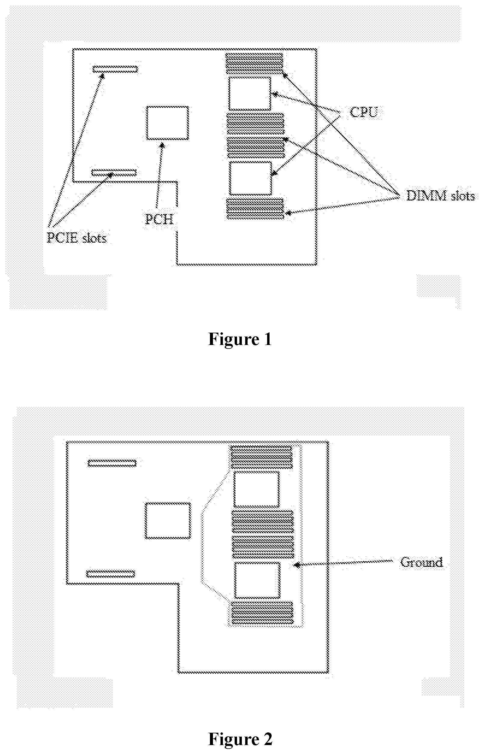
[0030] FIG. 1 is a schematic diagram showing a layout of a board;
[0031] FIG. 2 is a schematic diagram showing a layout of an L5 layer;
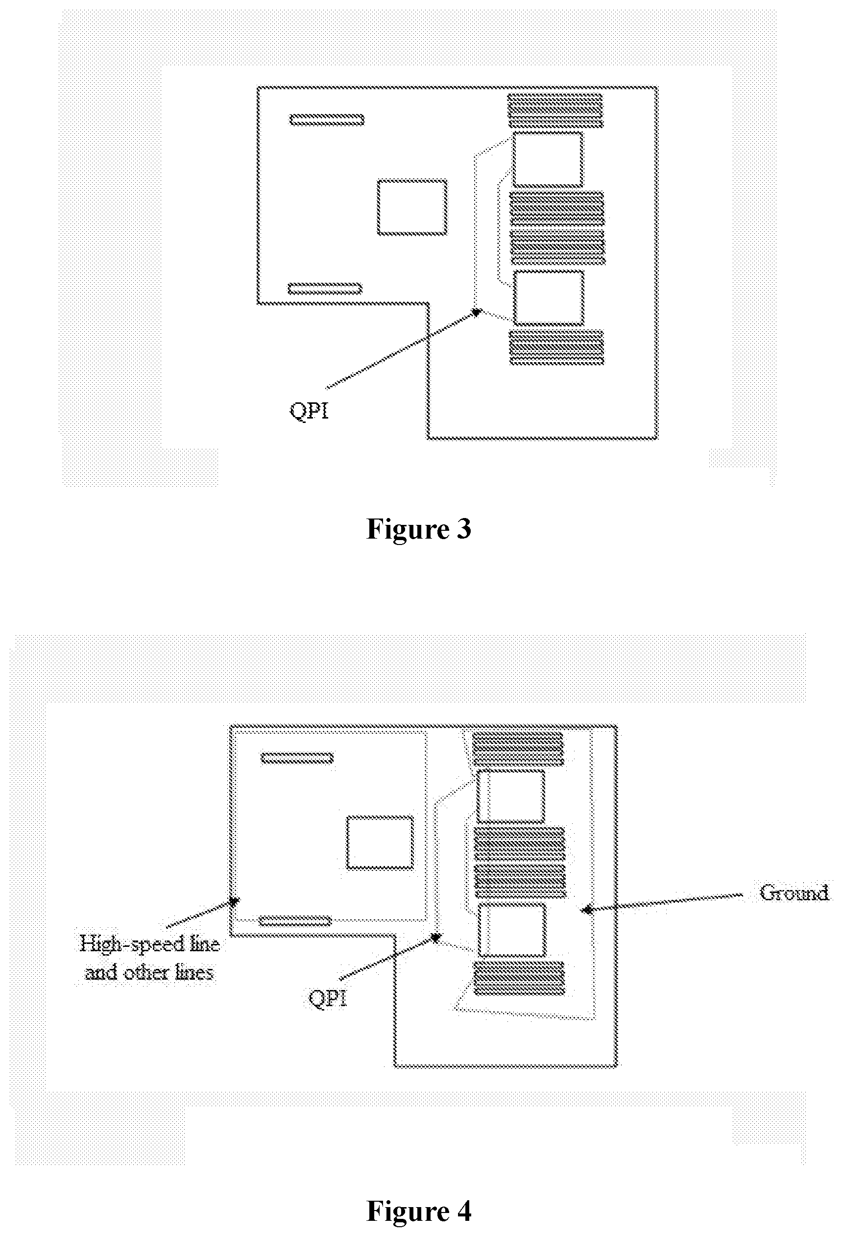
[0032] FIG. 3 is a schematic diagram showing a layout of an L4 layer;
[0033] FIG. 4 is a schematic diagram showing a layout of an L6 layer; and
[0034] FIG. 5 is a schematic diagram showing a layout of an L7 layer.
DETAILED DESCRIPTION
[0035] The present disclosure is described in detail in conjunction with the embodiments with reference to the drawings.
[0036] A method for layout and routing of a PCB includes the following steps 1) to 3).
[0037] In step 1), a shape of the PCB is determined and the main chips are arranged at appropriate positions on the PCB, including, as shown in FIG. 1, a region for arranging PCH (Platform Controller Hub) and PCIE (Peripheral Component Interconnect Express) slots, a region for arranging DIMM (dual-inline-memory-modules) slots and CPU (Central Processing Unit), and a region for QPI (Quick Path Interconnect) wiring, and the region for the QPI wiring is used for connecting two CPUs.
[0038] In step 2), a PCB including 10 stacked layers is provided, including L1 (TOP), L2, L3, L4, L5, L6, L7, L8 and L10 (BOT) from top to bottom.
[0039] In step 3), the L1 (TOP), L2, L3, L8, L9, L10 (BOT) layers are configured to have the conventional layout and routing, where:
[0040] the DDRs (double data rate) on the L3 layer and the DDR on the L8 layer are not changed, and the QPI signal lines are moved to the L5 layer and the L6 layer,
[0041] the high-speed lines and other lines in the conventional 12-layer structure is moved to the L3 layer and the L8 layer of the 10 layers,
[0042] a region of the L4 layer corresponding to the region for QPI wiring and the region for arranging DIMM slots and CPU is configured for a ground plane, and a remaining region of the L4 layer is configured for a power plane, as shown in FIG. 3,
[0043] a region of the L5 layer corresponds to the region for QPI wiring is configured for arranging QPI signal lines, with the ground plane on the L4 layer being a reference plane corresponding to the QPI signal lines, and a remaining region of the L5 layer is configured for a power plane, as shown in FIG. 2,
[0044] a region of the L6 layer corresponding to the region for QPI wiring is configured for arranging QPI signal lines, a region of the L6 layer corresponding to region for arranging PCH and PCIE slots is configured for arranging high-speed lines and other lines, and a region of the L6 layer corresponding to the region for arranging DIMM slots and CPU is configured for a ground plane, as shown in FIG. 4, and
[0045] a region of the L7 layer corresponding to the region of the L6 layer configured for arranging QPI signal lines and the region of the L6 layer configured for arranging high-speed lines and other lines is configured for a ground plane, for providing reference for the QPI signal lines and the high-speed lines on the L6 layer, and a remaining region of the L7 layer is configured for power supply, as shown in FIG. 5
[0046] The layout is as follows.
TABLE-US-00004 Layer Number Function Signal Line L1 TOP 1 oz PCIE, DDR L2 GND 1 oz Ground L3 Signal 1 oz DDR, High-speed line, other lines L4 Power/GND 2 oz Power supply, Ground L5 Power/Signal 1 oz QPI, Power supply L6 Signal/GND/Power 1 oz QPI, Ground, High-speed line, other lines L7 Power/GND 2 oz Power supply, Ground L8 Signal 1 oz DDR, High-speed line, other lines L9 GND 1 oz Ground L10 BOT 1 oz PCIE, DD
[0047] The embodiments are only used to illustrate the present disclosure and are not intended to limit the present disclosure. Those skilled in the technical art can make some variations and improvements without departing from the spirit and scope of the present disclosure. All the equivalent technical solutions are also within the scope of the present disclosure, and the scope of the present disclosure should be defined by the claims.
* * * * *
D00000
D00001
D00002
D00003
XML
uspto.report is an independent third-party trademark research tool that is not affiliated, endorsed, or sponsored by the United States Patent and Trademark Office (USPTO) or any other governmental organization. The information provided by uspto.report is based on publicly available data at the time of writing and is intended for informational purposes only.
While we strive to provide accurate and up-to-date information, we do not guarantee the accuracy, completeness, reliability, or suitability of the information displayed on this site. The use of this site is at your own risk. Any reliance you place on such information is therefore strictly at your own risk.
All official trademark data, including owner information, should be verified by visiting the official USPTO website at www.uspto.gov. This site is not intended to replace professional legal advice and should not be used as a substitute for consulting with a legal professional who is knowledgeable about trademark law.