Manufacturing of Carbon Nanotube Thin Film Transistor Backplanes and Display Integration Thereof
Li; Huaping
U.S. patent application number 16/678491 was filed with the patent office on 2020-04-23 for manufacturing of carbon nanotube thin film transistor backplanes and display integration thereof. This patent application is currently assigned to Carbon Nanotube Technologies, LLC. The applicant listed for this patent is Carbon Nanotube Technologies, LLC. Invention is credited to Huaping Li.
| Application Number | 20200127201 16/678491 |
| Document ID | / |
| Family ID | 70279704 |
| Filed Date | 2020-04-23 |


View All Diagrams
| United States Patent Application | 20200127201 |
| Kind Code | A1 |
| Li; Huaping | April 23, 2020 |
Manufacturing of Carbon Nanotube Thin Film Transistor Backplanes and Display Integration Thereof
Abstract
Methods for producing and integrating single-walled carbon nanotubes (SWCNT) into existing TFT backplane manufacturing lines are provided. In contrast to LTPS and oxide TFT backplanes, SWCNT TFT backplanes exhibit either equivalent or better figures of merit such as high field emission mobility, low temperature fabrication, good stability, uniformity, scalability, flexibility, transparency, mechanical deformability, low voltage and low power, bendability and low cost. Methods and processes for integrating SWCNTs technologies into existing TFT backplane manufacturing lines, pilot test and mass production can start without additional capex needs are also provided.
| Inventors: | Li; Huaping; (Los Angeles, CA) | ||||||||||
| Applicant: |
|
||||||||||
|---|---|---|---|---|---|---|---|---|---|---|---|
| Assignee: | Carbon Nanotube Technologies,
LLC Los Angeles CA |
||||||||||
| Family ID: | 70279704 | ||||||||||
| Appl. No.: | 16/678491 | ||||||||||
| Filed: | November 8, 2019 |
Related U.S. Patent Documents
| Application Number | Filing Date | Patent Number | ||
|---|---|---|---|---|
| 15589896 | May 8, 2017 | |||
| 16678491 | ||||
| 62758376 | Nov 9, 2018 | |||
| Current U.S. Class: | 1/1 |
| Current CPC Class: | H01L 27/283 20130101; H01L 51/0048 20130101; H01L 51/0003 20130101; H01L 27/3274 20130101; H01L 51/0018 20130101; H01L 51/0545 20130101; H01L 2227/323 20130101; H01L 51/0558 20130101 |
| International Class: | H01L 51/00 20060101 H01L051/00; H01L 51/05 20060101 H01L051/05; H01L 27/28 20060101 H01L027/28; H01L 27/32 20060101 H01L027/32 |
Claims
1. A method for manufacturing a single-walled carbon nanotube thin film transistor backplane comprising: providing a substrate; patterning a gate electrode and dielectric layer on the substrate to form a channel; depositing a solution of a thin-film layer of single-walled carbon nanotubes on said dielectric layer to form a back-layer; and patterning at least a n+ layer, and a drain and a source electrode on the back-layer using a photomask and photolithography process such that the portion of the back-layer overlapping the channel is exposed.
2. The method of claim 1, wherein the back-layer is deposited by a spraying technique selected from the group consisting of aerosol spray, air spray and ultrasonic spray.
3. The method of claim 2, wherein the single-walled carbon nanotube aerosol is formed from an aqueous solution of single-walled carbon nanotubes that are ultrasonicated in an ultrasonicating nozzle and emitted in a carrier gas flow.
4. The method of claim 1, wherein the back-layer is printed atop the substrate using aerosol jet printing as a single-walled carbon nanotube aerosol.
5. The method of claim 4, wherein the single-walled carbon nanotube aerosol is formed by a technique selected from ultrasonic atomization and pneumatic atomization.
6. The method of claim 1, wherein the single-walled carbon nanotubes adhere onto the dielectric through hydrophobicity forces with a peel off force of at least 4.35 N/cm.sup.2.
7. The method of claim 1, wherein the substrate comprises at least a Gen 4.5 glass.
8. The method of claim 1, wherein the single-walled carbon nanotubes are high purity single chirality single-walled carbon nanotubes.
9. The method of claim 8, wherein the single-walled carbon nanotubes have an index selected from (6,4), (9,1), (8,3), (6,5), (7,3), (7,5), (10,2), (8,4), (7,6), (9,2), and mixtures thereof.
10. The method of claim 1, wherein the single-walled carbon nanotube thin film is formed of a plurality of discrete thin films.
11. The method of claim 1, further comprising depositing and patterning an etch stop layer atop the back-layer such that the etch stop overlaps the channel.
12. The method of claim 1, wherein further comprising treating the single-walled carbon nanotube thin film with an acidic etch.
13. The method of claim 12, wherein the acidic etch is selected from a group consisting of 5% H.sub.3PO.sub.4, 15% HNO.sub.3, and 5% Acetic Acid.
14. The method of claim 1, further comprising washing the treated single-walled carbon nanotube thin film.
15. The method of claim 1, further comprising sintering the single-walled carbon nanotube thin film at a temperature of at least 1100.degree. C.
16. The method of claim 1, wherein the thin films are formed with subthreshold leakage current comprising: spin coating a photoresist on the single-walled carbon nanotube thin film; defining a pattern atop the photoresist by photolithography to create regions of a defined photoresist and undefined photoresist; solution developing the defined pattern to form a developed photoresist; and plasma or wet etching the single-walled carbon nanotubes thin film using the developed photoresist to form a patterned single-walled carbon nanotube thin film.
17. The method of claim 1, wherein the patterning comprises a chemical vapor deposition technique.
18. The method of claim 17, wherein the patterning includes the use of a SiN.sub.x material.
19. The method of claim 17, wherein the chemical vapor deposition technique comprises one of either a Unaxis 790 or STS device.
20. The method of claim 19, wherein the chemical vapor deposition technique uses a Unaxis 790 device with a ratio of ammonium to silane of 10 to 5.3 sccm.
21. The method of claim 19, wherein the chemical vapor deposition technique uses an STS device with a ratio of ammonium to silane of around 1 to 1 sccm.
Description
CROSS-REFERENCE TO RELATED APPLICATIONS
[0001] The current application is a continuation-in-part of U.S. patent application Ser. No. 15/589,896, filed May 8, 2017, and claims priority to U.S. Provisional Patent Application No. 62/758,376, filed Nov. 9, 2018, the disclosures of which is incorporated herein by reference in their entireties.
FIELD OF THE INVENTION
[0002] Methods for manufacturing carbon nanotube thin film transistor backplanes and their integration into displays under industrial conditions.
BACKGROUND OF THE INVENTION
[0003] Flat Panel Displays (FPDs) have infiltrated consumer electronics that are integrated with display functions. Among existing FPDs, Thin film transistor (TFT)--liquid crystal displays (LCDs) dominate the current display marketplace with a 97.5% market share in 2013 even though there are certain limitations on color, contrast, and response time. More recently, display capital expenditures have rapidly shifted from TFT-LCDs to AMOLEDs, not only because of the superior display qualities of color, contrast and response time, but also large AMOLEDs in Gen 8 or larger fabrications have a cost edge over TFT-LCDs. To be able to fabricate greater than Gen 8 size AMOLEDs, there are several technology challenges, including limitations in conventional active matrix thin-film transistor (TFT) backplanes. (See, e.g., G. Gu and S. R. Forrest, IEEE Journal of Selected Topics in Quantum Electronics, vol. 4, pp. 83-99, 1998, the disclosure of which is incorporated herein by reference.)
[0004] The current active matrix TFT backplanes used to drive AM-LCD pixels are typically made of amorphous silicon (a-Si), which has a low mobility (-1 cm.sup.2V.sup.-1s.sup.-1) and poor stability, and is therefore unsuitable for AMOLED pixels. (See, M. J. Powell, IEEE Transactions on Electron Devices, vol. 36, pp. 2753-2763, 1989, the disclosure of which is incorporated herein by reference.) As a result of these deficiencies, currently AMOELD displays are driven by low temperature polycrystalline silicon (poly-Si) TFTs that suffer from high fabrication cost and time, and device size, orientation, and inhomogeneity limitations, all of which present a severe challenge to increasing display size and production yield. (See, e.g., C. -P. Chang and Y.-C. S. Wu, IEEE electron device letters, vol. 30, pp. 130-132, 2009; Y.-J. Park, M.-H. Jung, S.-H. Park and O. Kim, Japanese Journal of Applied Physics, vol. 49, pp. 03CD01, 2010; and P.-S. Lin, and T.-S. Li, IEEE electron device letters, vol. 15, pp. 138-139, 1994, each of the disclosures of which are incorporated herein by reference.)
[0005] Although low temperature polycrystalline silicon (LTPS) backplanes have been under mass production up to Gen 5.5, LTPS fabrication techniques including excimer laser annealing (ELA) and advanced solid phase crystallization (ASPC) creates substantial hurdles for >Gen 8 scale-up. For example, both ELA and ASPC fabs have a very slow total average cycle time, more than twice of the typical 60 sec for a-Si. This doubles the capital cost for the array process of a-Si. Additionally, scale-up of ELA could cause non-uniformity and array failure. The high temperature of the ASPC process (.about.600.degree. C.) requires expensive glass to avoid glass warping and shrinkage. (B. Young, Information Display, vol. 10, pp. 24, 2010, the disclosure of which is incorporated herein by reference.) The higher processing temperatures and more complicated photomask required to manufacture LTPS increases capex and the difficulty of achieving high yield rates. This makes a 5'' LTPS TFT-LCD (1920.times.1080 pixels) 14% more expensive than a same size a-Si TFT-LCD.
[0006] Accordingly, a need exists for manufacturing techniques to allow for the production of less expensive TFT backplanes.
SUMMARY OF THE INVENTION
[0007] Methods for manufacturing carbon nanotube thin film transistor backplanes and their integration into displays are provided.
[0008] Many embodiments are directed to methods for manufacturing a single-walled carbon nanotube thin film transistor backplane including: [0009] providing a substrate; [0010] depositing an insulator comprised of a thin-film layer of single-walled carbon nanotubes atop said substrate; and [0011] patterning at least a drain and a source electrode, a dielectric, one or more top-gated electrodes and one or more pixel electrodes atop the insulator using a photomask and photolithography process.
[0012] In other embodiments the insulator is deposited by a spraying technique selected from the group consisting of aerosol spray, air spray and ultrasonic spray.
[0013] In some such embodiments the single-walled carbon nanotube aerosol is formed by a technique selected from ultrasonic atomization at a voltage that ranges from 20 to 48 V, and pneumatic atomization with about 600 cubic centimeters per minute atomizer flow to generate aerosol in diameter of about 1 to 5 .mu.m; and wherein the aerosol is brought to a spraying head by a carrier gas flow of from about 10 to 20 cubic centimeters per minute.
[0014] In still other such embodiments the single-walled carbon nanotube aerosol is formed from an aqueous solution of single-walled carbon nanotubes that are ultrasonicated in an ultrasonicating nozzle and emitted in a carrier gas flow of from about 10 to 20 cubic centimeters per minute.
[0015] In yet other embodiments the insulator is printed atop the substrate using aerosol jet printing as a single-walled carbon nanotube aerosol.
[0016] In some such embodiments the single-walled carbon nanotube aerosol is formed by a technique selected from ultrasonic atomization at a voltage that ranges from 20 to 48 V and pneumatic atomization with .about.600 cubic centimeters per minute atomizer flow to generate the aerosol in a diameter of from 1 to 5 .mu.m; and wherein the aerosol is brought to a fine nozzle of less than 100 .mu.m by a carrier gas flow of from 10 to 20 cubic centimeters per minute and focused with a sheath gas flow of from 25 to 50 ccm.
[0017] In other such embodiments the deposited linewidth is less than 10 .mu.m with a <2 .mu.m registration accuracy.
[0018] In still other embodiments the single-walled carbon nanotubes are high purity single chirality single-walled carbon nanotubes.
[0019] In some such embodiments the single-walled carbon nanotubes have an index selected from (6,4), (9,1), (8,3), (6,5), (7,3), (7,5), (10,2), (8,4), (7,6), (9,2), and mixtures thereof.
[0020] In still yet other embodiments the single-walled carbon nanotube thin film is formed of a plurality of discrete thin films.
[0021] In some such embodiments the discrete single-walled carbon nanotube thin films are patterned using one photomask photolithography process.
[0022] In still yet other embodiments the method further includes treating the single-walled carbon nanotube thin film with acidic gas.
[0023] In some such embodiments the acidic gas is deposited via aerosol spraying.
[0024] In still some other such embodiments the method further includes washing the treated single-walled carbon nanotube thin film with isopropanol.
[0025] In yet some other such embodiments the method further includes sintering the single-walled carbon nanotube thin film at a temperature from around 100 to 200.degree. C.
[0026] In still yet other embodiments the thin films are formed with subthreshold leakage current including: [0027] spin coating a photoresist on the single-walled carbon nanotube thin film; [0028] defining a pattern atop the photoresist by photolithography to create regions of a defined photoresist and undefined photoresist; [0029] solution developing the defined pattern to form a developed photoresist; and [0030] plasma or wet etching the single-walled carbon nanotubes thin film using the developed photoresist to form a patterned single-walled carbon nanotube thin film.
[0031] In still yet other embodiments the method includes integrating the single-walled carbon nanotube thin film transistor backplane into a display device.
[0032] Various other embodiments are directed to systems configured to deposit a single-walled carbon nanotube thin film transistor backplane including: [0033] a plurality of printer heads mounted in association with a moving station; [0034] the plurality of printer heads in fluid communication with a solution of an aqueous solution of single-walled carbon nanotubes for depositing a thin film of the single-walled carbon nanotubes atop a substrate disposed on the moving station; and [0035] wherein the printer heads are integrated with a photomask and photolithography process for patterning and forming at least a drain and a source electrode, a dielectric, one or more top-gated electrodes and one or more pixel electrodes atop the deposited thin film.
[0036] Some other embodiments are directed to methods for manufacturing a single-walled carbon nanotube thin film transistor backplane including: [0037] providing a substrate; [0038] patterning a gate electrode and dielectric layer on the substrate to form a channel; [0039] depositing a solution of a thin-film layer of single-walled carbon nanotubes on said dielectric layer to form a back-layer; and [0040] patterning at least a n+ layer, and a drain and a source electrode on the back-layer using a photomask and photolithography process such that the portion of the back-layer overlapping the channel is exposed.
[0041] In some such embodiments the back-layer is deposited by a spraying technique selected from the group consisting of aerosol spray, air spray and ultrasonic spray.
[0042] In still some such embodiments the single-walled carbon nanotube aerosol is formed from an aqueous solution of single-walled carbon nanotubes that are ultrasonicated in an ultrasonicating nozzle and emitted in a carrier gas flow.
[0043] In yet some such embodiments the back-layer is printed atop the substrate using aerosol jet printing as a single-walled carbon nanotube aerosol.
[0044] In still yet some such embodiments the single-walled carbon nanotube aerosol is formed by a technique selected from ultrasonic atomization and pneumatic atomization.
[0045] In still yet some such embodiments the single-walled carbon nanotubes adhere onto the dielectric through hydrophobicity forces with a peel off force of at least 4.35 N/cm.sup.2.
[0046] In still yet some such embodiments the substrate comprises at least a Gen 4.5 glass.
[0047] In still yet some such embodiments the single-walled carbon nanotubes are high purity single chirality single-walled carbon nanotubes.
[0048] In still yet some such embodiments the single-walled carbon nanotubes have an index selected from (6,4), (9,1), (8,3), (6,5), (7,3), (7,5), (10,2), (8,4), (7,6), (9,2), and mixtures thereof.
[0049] In still yet some such embodiments the single-walled carbon nanotube thin film is formed of a plurality of discrete thin films.
[0050] In still yet some such embodiments the methods further include depositing and patterning an etch stop layer atop the back-layer such that the etch stop overlaps the channel.
[0051] In still yet some such embodiments the methods further include treating the single-walled carbon nanotube thin film with an acidic etch.
[0052] In still yet some such embodiments the acidic etch is selected from a group consisting of 5% H.sub.3PO.sub.4, 15% HNO.sub.3, and 5% Acetic Acid.
[0053] In still yet some such embodiments further include washing the treated single-walled carbon nanotube thin film.
[0054] In still yet some such embodiments further include sintering the single-walled carbon nanotube thin film at a temperature of at least 1100.degree. C.
[0055] In still yet some such embodiments the thin films are formed with subthreshold leakage current including: [0056] spin coating a photoresist on the single-walled carbon nanotube thin film; [0057] defining a pattern atop the photoresist by photolithography to create regions of a defined photoresist and undefined photoresist; [0058] solution developing the defined pattern to form a developed photoresist; and [0059] plasma or wet etching the single-walled carbon nanotubes thin film using the developed photoresist to form a patterned single-walled carbon nanotube thin film.
[0060] In still yet some such embodiments the patterning comprises a chemical vapor deposition technique.
[0061] In still yet some such embodiments the patterning includes the use of a SiN.sub.x material.
[0062] In still yet some such embodiments the chemical vapor deposition technique comprises one of either a Unaxis 790 or STS device.
[0063] In still yet some such embodiments the chemical vapor deposition technique uses a Unaxis 790 device with a ratio of ammonium to silane of 10 to 5.3 sccm.
[0064] In still yet some such embodiments the chemical vapor deposition technique uses an STS device with a ratio of ammonium to silane of around 1 to 1 sccm.
[0065] Additional embodiments and features are set forth in part in the description that follows, and in part will become apparent to those skilled in the art upon examination of the specification or may be learned by the practice of the invention. A further understanding of the nature and advantages of the present invention may be realized by reference to the remaining portions of the specification and the drawings, which forms a part of this disclosure.
BRIEF DESCRIPTION OF THE DRAWINGS
[0066] The description will be more fully understood with reference to the following figures and data graphs, which are presented as exemplary embodiments of the invention and should not be construed as a complete recitation of the scope of the invention, wherein:
[0067] FIGS. 1a and 1b provide data graphs showing the absorption spectrum and electrical properties of single-wall carbon nanotubes in accordance with embodiments of the invention.
[0068] FIGS. 2a and 2b provide schematic illustrations of exemplary vertical light emitting transistors in accordance with embodiments of the invention.
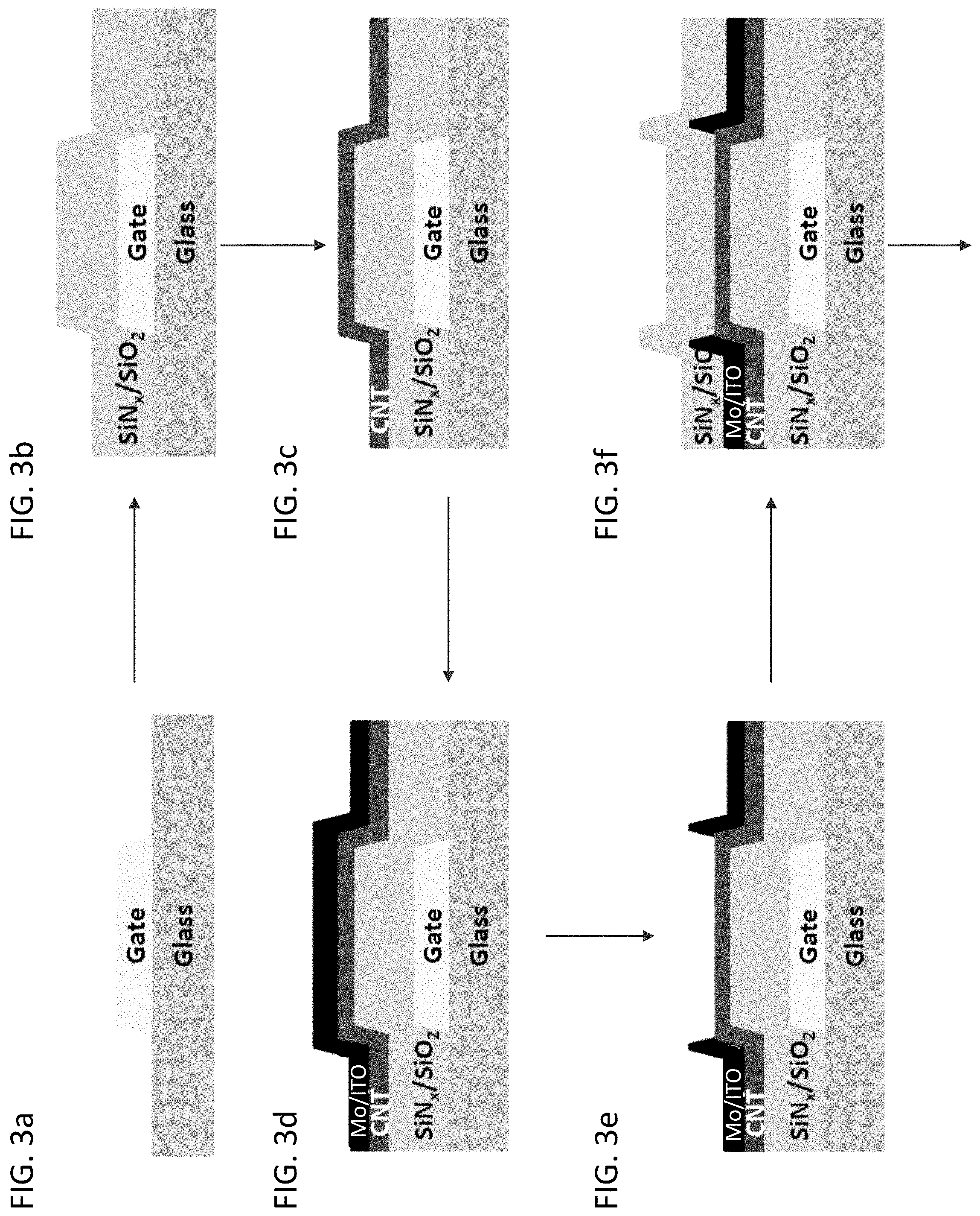
[0069] FIGS. 3a-3k provide schematic illustrations of methods of forming etch-stop vertical light emitting transistors in accordance with embodiments.
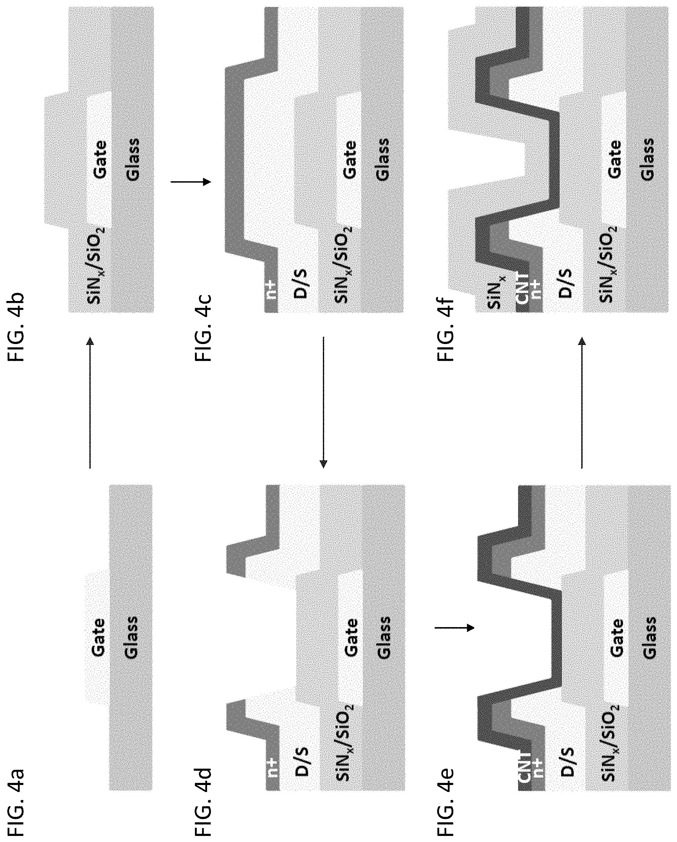
[0070] FIGS. 4a-4f provide schematic illustrations of methods of forming vertical light emitting transistors in accordance with embodiments.
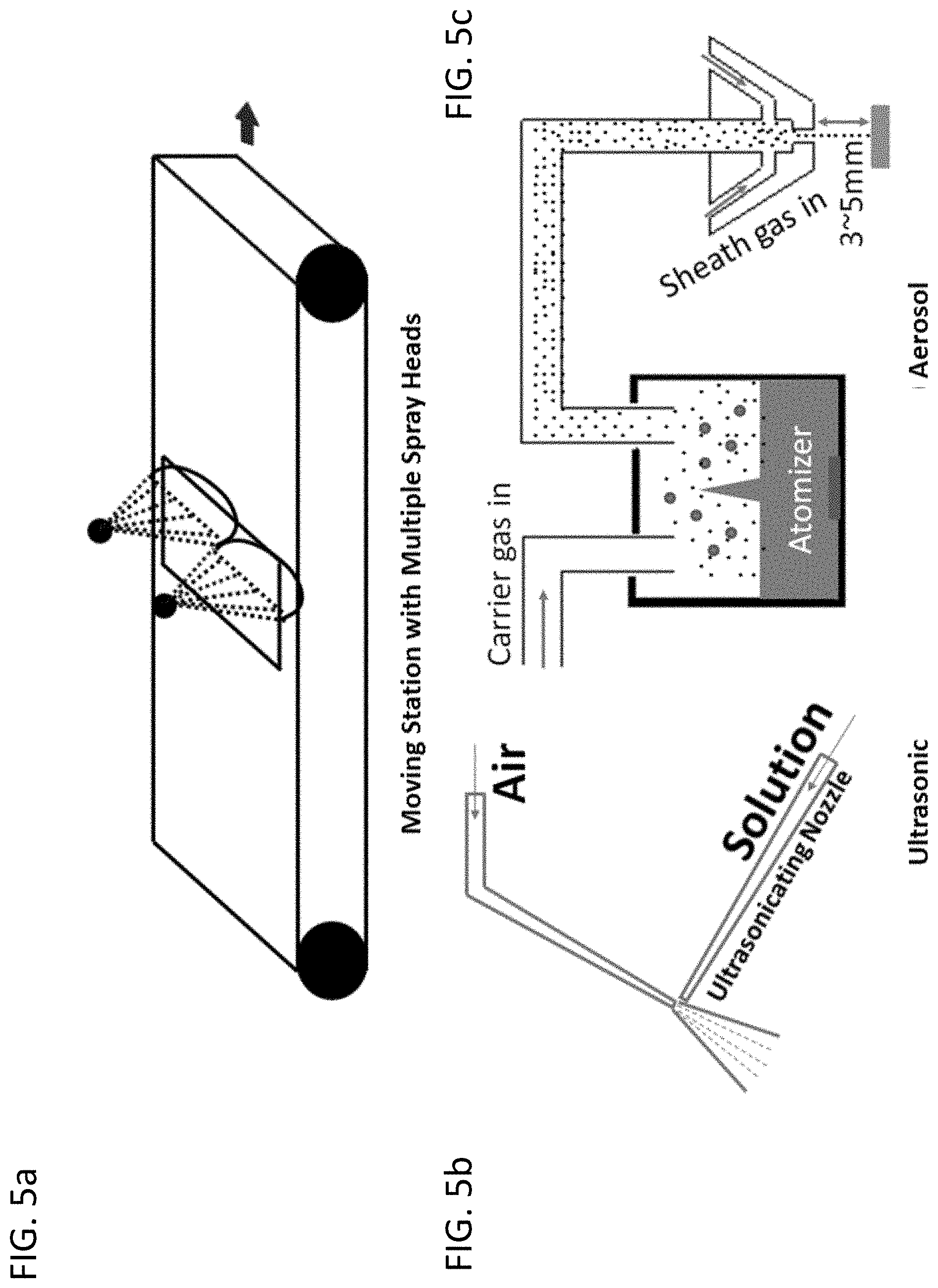
[0071] FIGS. 5a to 5c provide schematic illustrations showing: a) multiple spray heads for solution spraying devices in moving stations, b) an airbrush for ultrasonic spray, and c) aerosol spray system, each in accordance with embodiments of the invention.
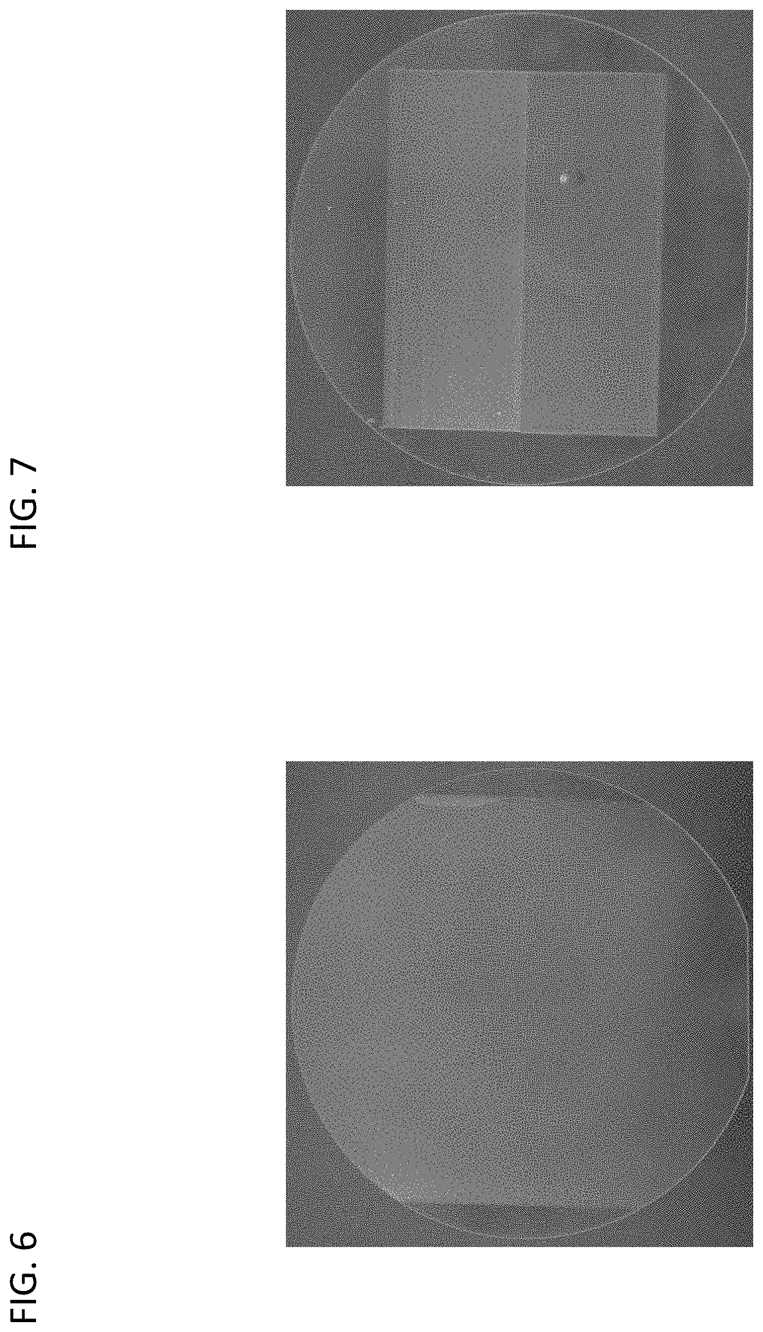
[0072] FIG. 6 provides an image of an airbrush sprayed carbon nanotube thin film in accordance with embodiments of the invention.
[0073] FIG. 7 provides an image of an aerosol sprayed carbon nanotube thin film in accordance with embodiments of the invention.
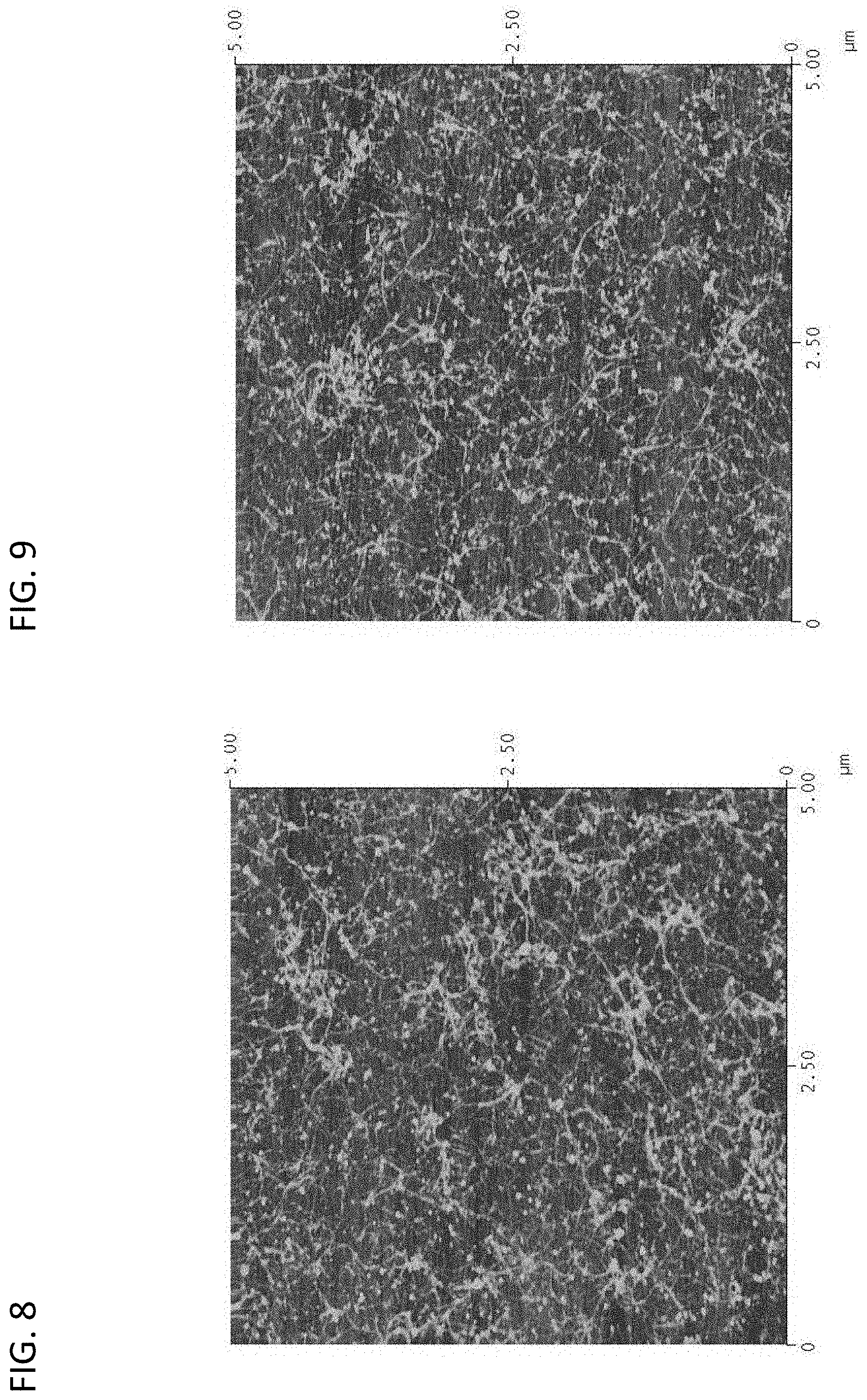
[0074] FIG. 8 is an atomic force microscope (AFM) image of an airbrush sprayed single-walled carbon nanotube thin film in accordance with embodiments of the invention.
[0075] FIG. 9 is an atomic force microscope (AFM) image of an aerosol sprayed single-walled carbon nanotube thin film in accordance with embodiments of the invention.
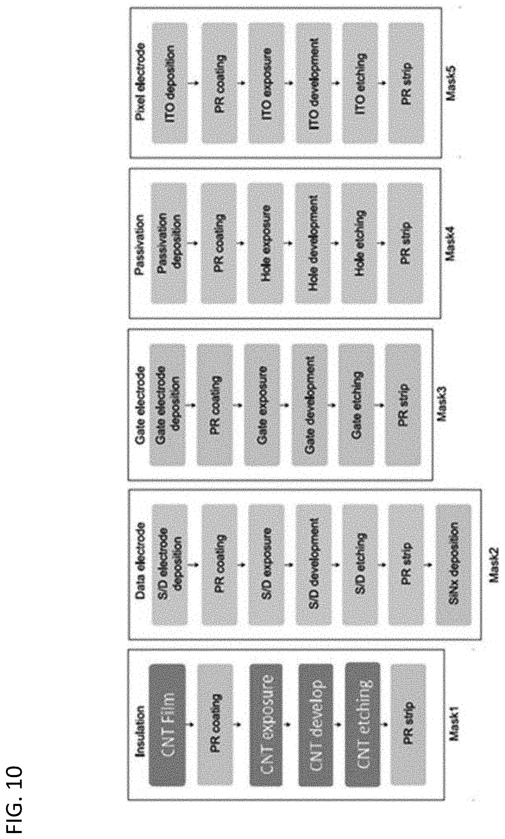
[0076] FIG. 10 provides a flowchart showing a fabrication process for manufacturing top-gated carbon nanotube TFT backplanes in accordance with embodiments of the invention.
[0077] FIG. 11 provides an image of an aerosol printer for printing carbon nanotube patters on drain/source marks in accordance with embodiments of the invention.
[0078] FIG. 12 provides a photo and optic image of drain/source marks before aerosol printing single-walled carbon nanotube patterned films in accordance with embodiments of the invention.
[0079] FIG. 13 provides a photo and optic image of aerosol printed single-walled carbon nanotube patterned films on drain/source marks in accordance with embodiments of the invention.
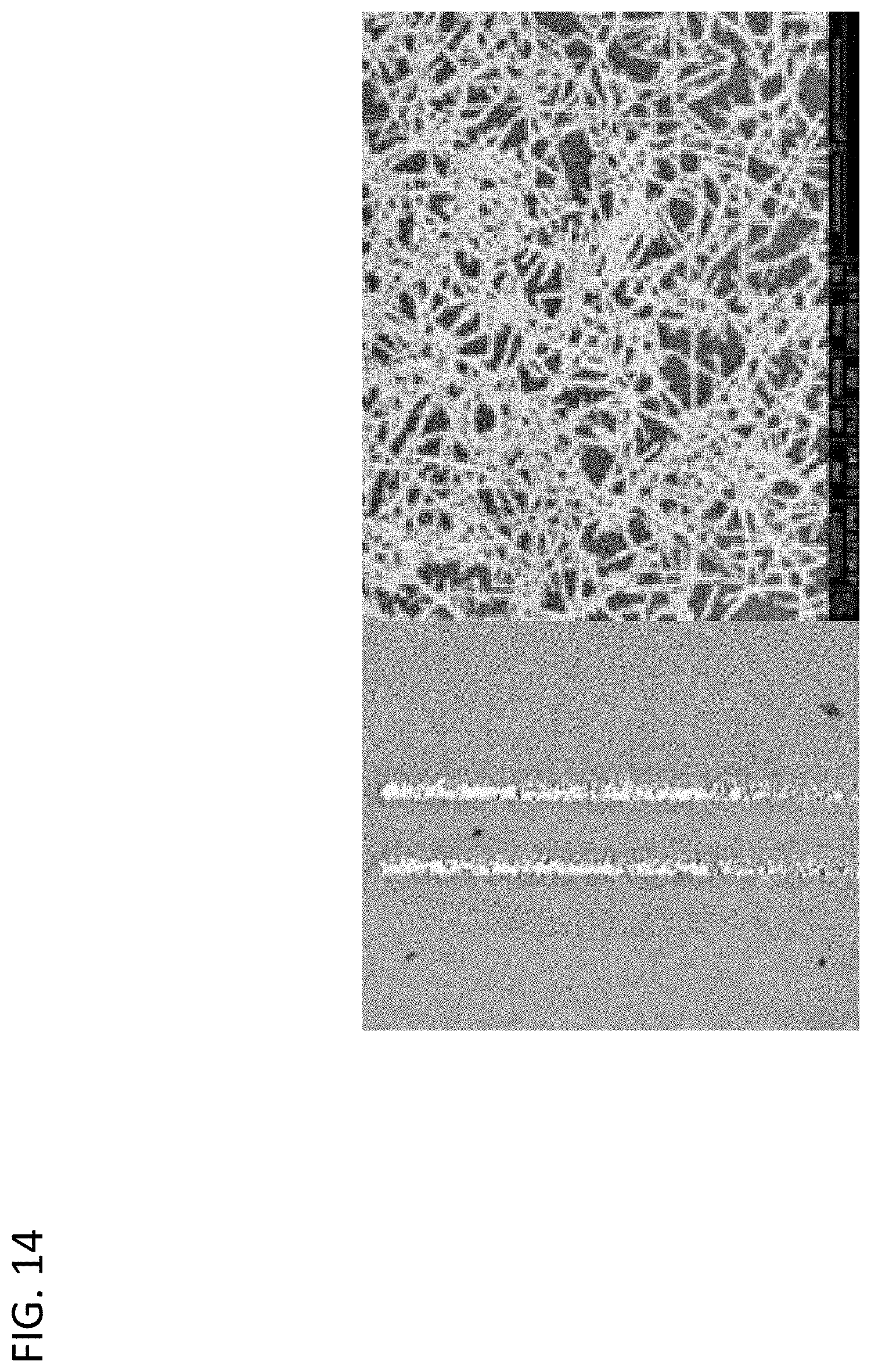
[0080] FIG. 14 provides an optic image of aerosol jet printed carbon nanotube films, and where the inset is an SEM image, in accordance with embodiments of the invention.
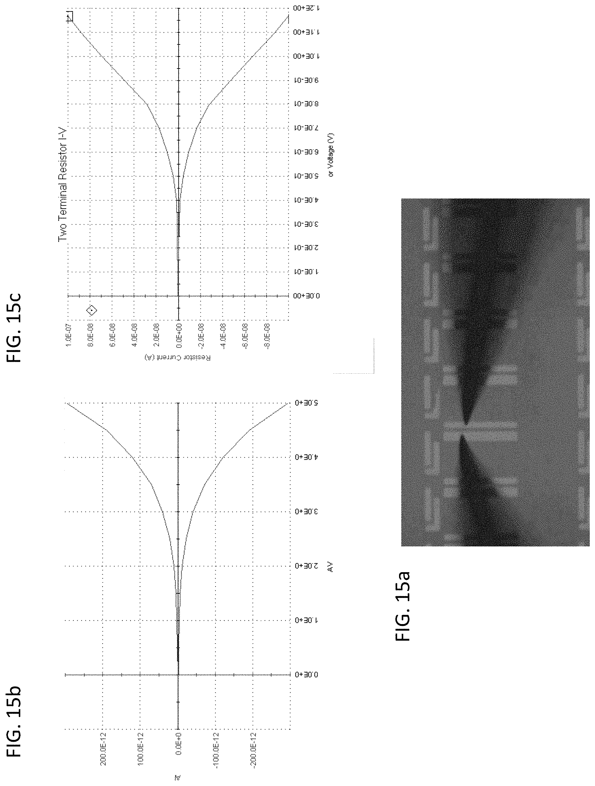
[0081] FIG. 15a provides an optic image of aerosol jet printed carbon nanotube films on photolithography patterned electrodes, and where the FIGS. 15b and 15c are I-V curves of such carbon nanotube films showing pure semiconductor properties, in accordance with embodiments of the invention.
[0082] FIG. 16 provides a photo image of an apparatus having multiple aerosol jet printer heads mounted on a roll-to-roll station in accordance with embodiments of the invention.
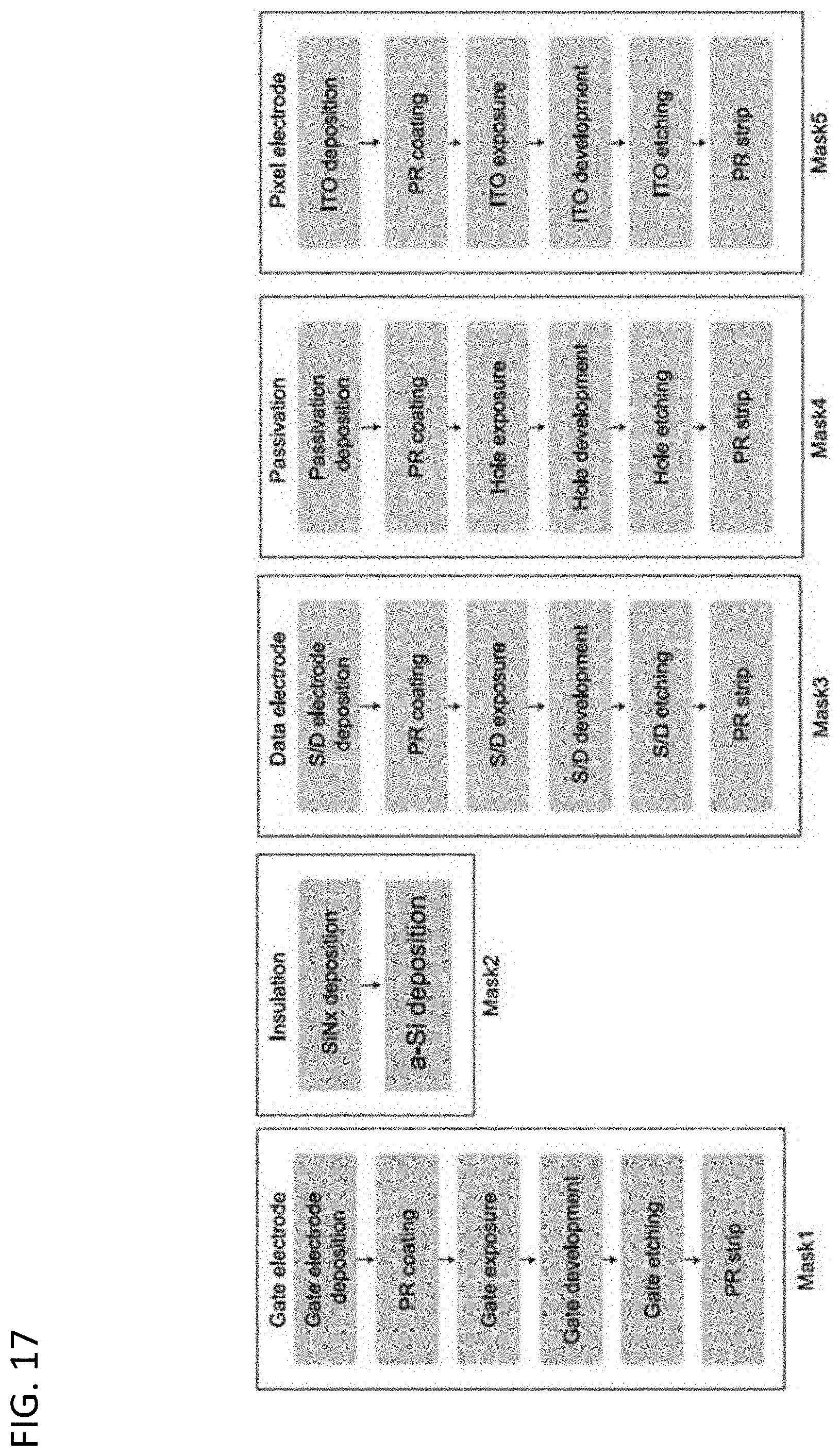
[0083] FIG. 17 provides a flowchart showing a fabrication process for manufacturing a standard bottom-gated a-Si TFT backplane in accordance with the prior art.
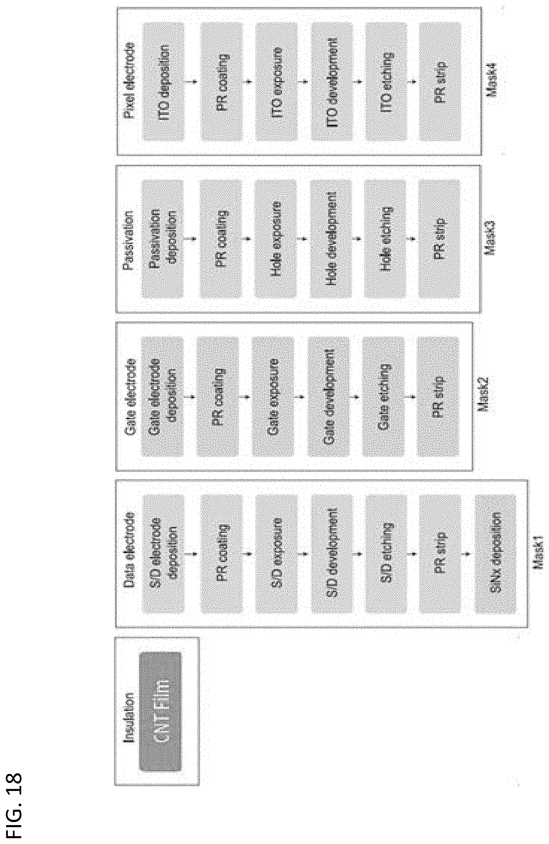
[0084] FIG. 18 provides a flowchart showing a fabrication process for manufacturing top-gated carbon nanotube TFT backplanes in accordance with embodiments of the invention.
[0085] FIG. 19 provides a flowchart showing a fabrication process for manufacturing a top-gated printed carbon nanotube TFT backplanes in accordance with embodiments of the invention.
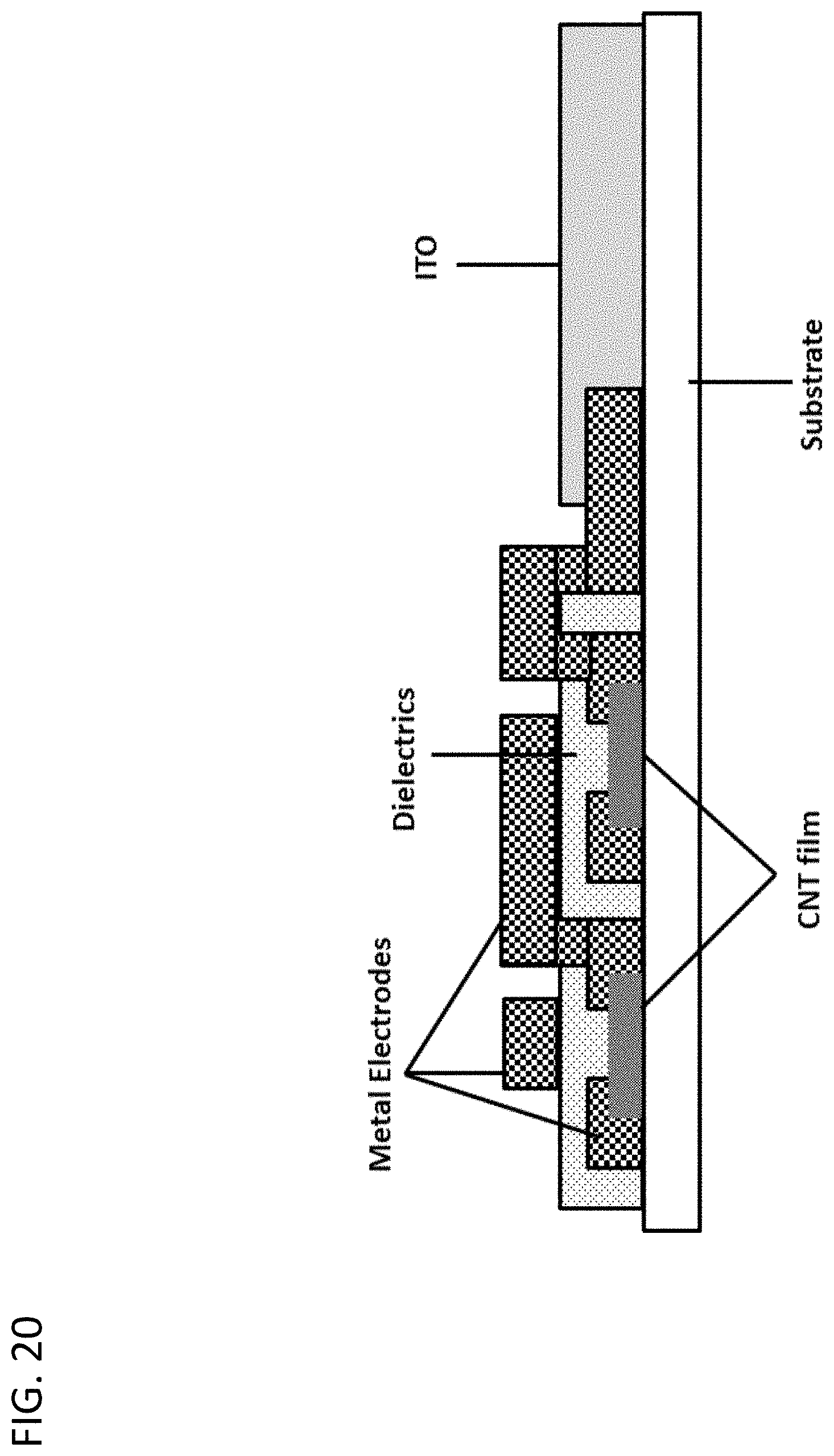
[0086] FIG. 20 provides a cross-sectional view of a single-walled carbon nanotube thin film transistor in accordance with embodiments of the invention.
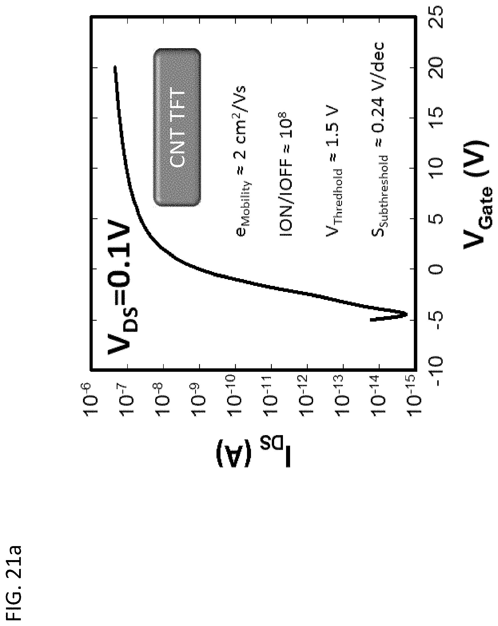
[0087] FIGS. 21a to 21c provide data graphs illustrating transfer characteristic comparisons of: (a carbon nanotube thin film transistors according to embodiments; (b traditional amorphous silicon thin film transistors; and (c metal oxide thin film transistors.
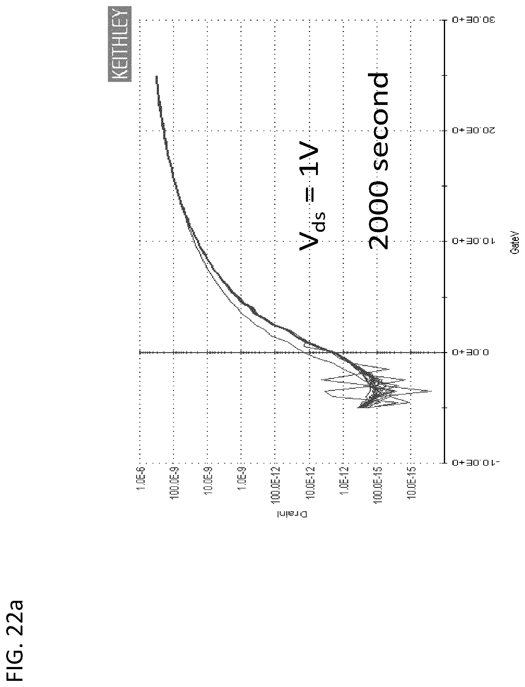
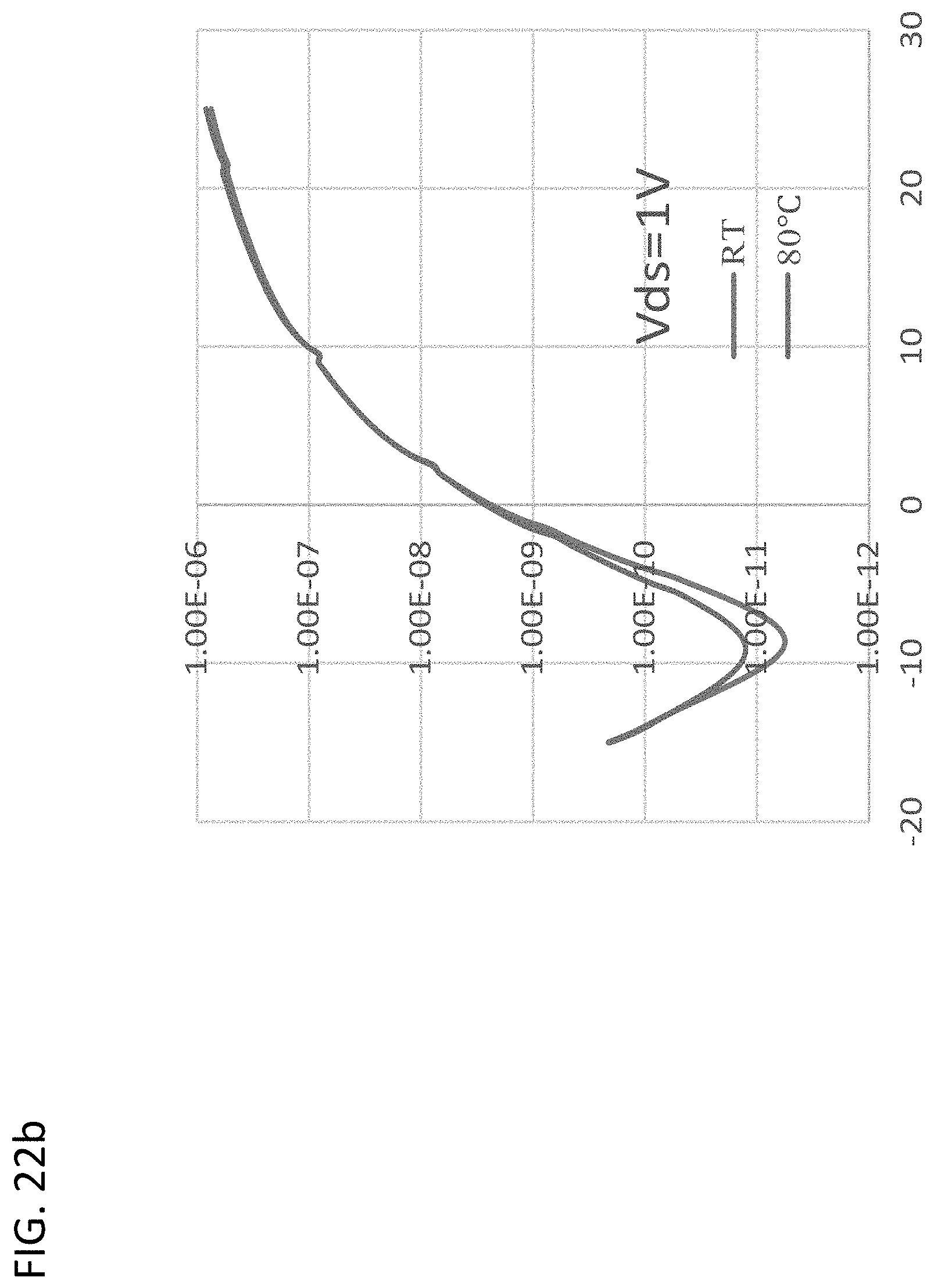
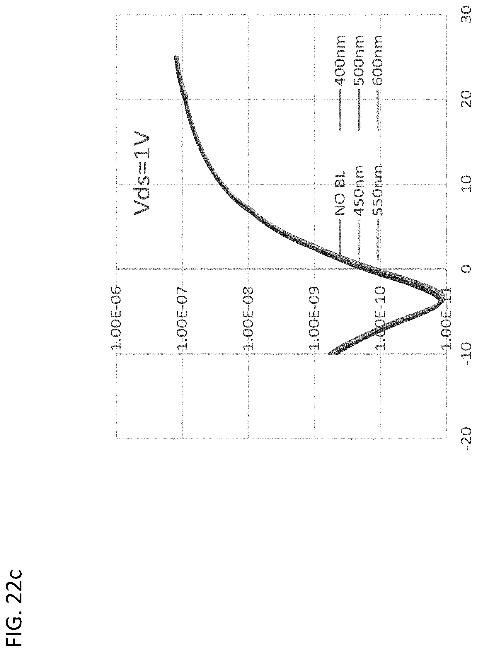
[0088] FIGS. 22a to 22c provide transfer curves of CNT TFTs according to embodiments after: (a 2000 seconds stress under 10 V gate; (b temperature stability; and (c photostability.
[0089] FIG. 23 provides a photographic image of Gen 4.5 glass coated with carbon nanotubes using a solution process according to embodiments.
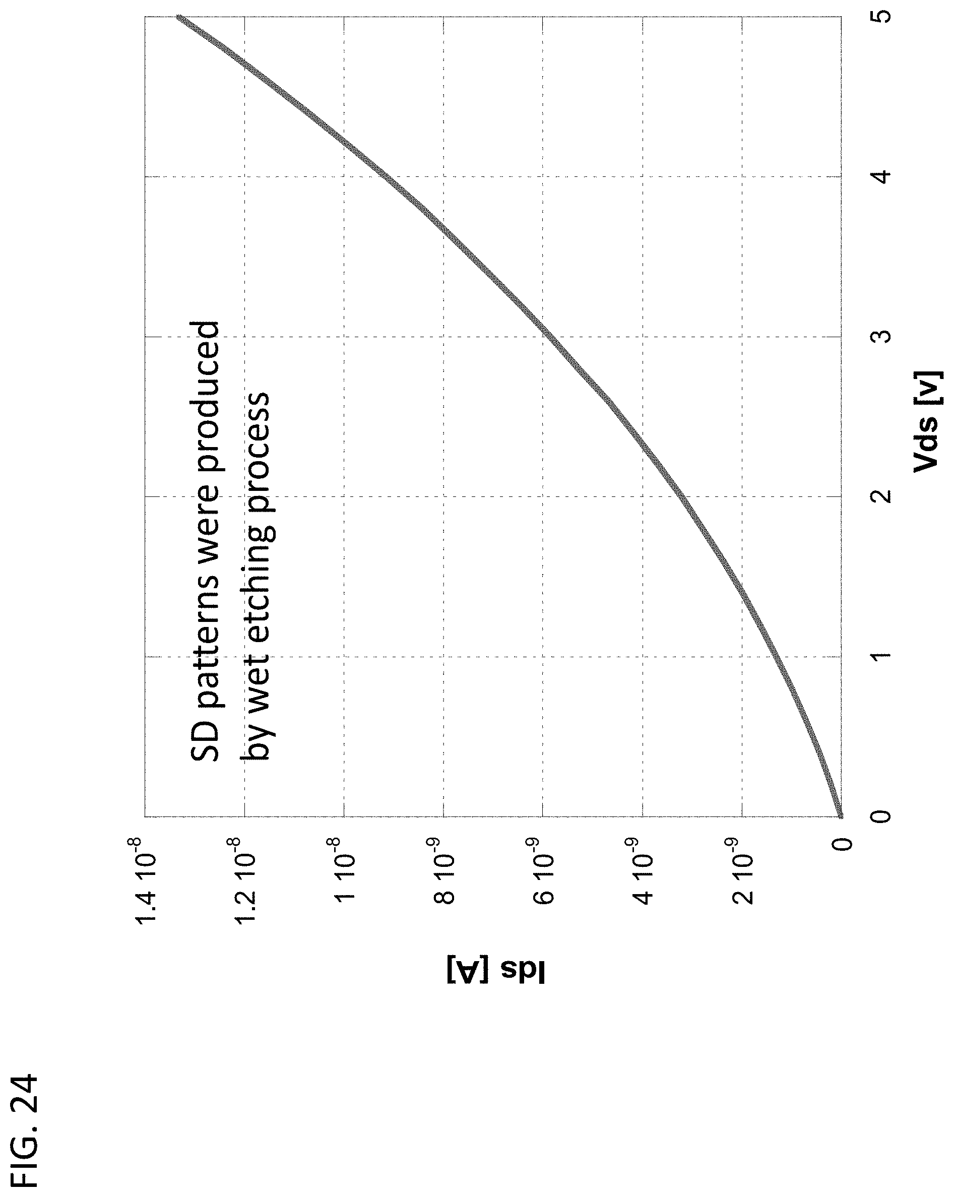
[0090] FIG. 24 provides an I-V curve of Al electrodes on carbon nanotube thin films after wet etch using acids according to embodiments.
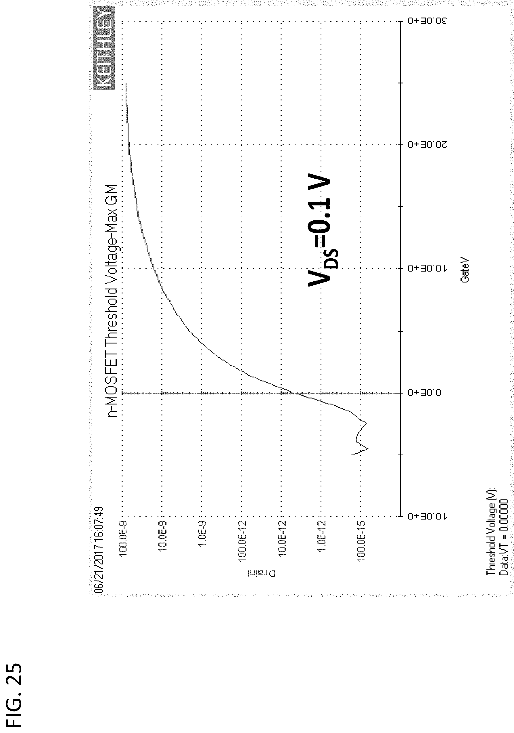
[0091] FIG. 25 provides data graphs illustrating transfer characteristics of carbon nanotube thin film transistors with SiNx deposited using STS PECVD according to embodiments.
DETAILED DESCRIPTION OF THE INVENTION
[0092] Turning to the drawings, devices, materials and methods for producing and integrating single-walled carbon nanotubes (SWCNT) into existing TFT backplane manufacturing lines. In particular, in contrast to LTPS and oxide TFT backplanes, SWCNT TFT backplanes exhibit either equivalent or better figures of merit such as high field emission mobility, low temperature fabrication, good stability, uniformity, scalability, flexibility, transparency, mechanical deformability, low voltage and low power, bendability and low cost. Accordingly, many embodiments are directed to methods and process for integrating SWCNTs technologies into existing TFT backplane manufacturing lines, pilot test and mass production can start without additional capex needs. Moreover, other embodiments are directed to methods and processes for integrating such SWCNT TFT backplanes into video displays, including, in various embodiments high-end glassless 3-D and ultra-definition panel displays such as Helmet-Mounted Display (HMD). In the following text, carbon nanotubes refer to single-walled carbon nanotubes, including high purity single chirality SWCNT, such as SWCNTs with indexes of (6,4), (9,1), (8,3), (6,5), (7,3), (7,5), (10,2), (8,4), (7,6), (9,2) and mixtures thereof.
[0093] Active matrix organic light emitting displays (AMOLEDs) are highly attractive due to their power saving, ultra-high definition, and broad viewing angles. In particular, advances in organic light emitting transistors (OLETs) exhibit improved external efficiency over organic light emitting diodes (OLEDs) by directly modulating charge carriers of light emitting materials. Further, inducing a vertical structure in OLETs circumvents the intrinsic low mobility of organic materials by providing short channel length, thereby making it possible to achieve high conductance at low power and low voltages, thus enhancing the energy conversion efficiency, the lifetime and stability of the organic materials. Moreover, combining thin film transistor (TFT) switching and
[0094] OLED light emitting properties in a single device leads to a simplified fabrication process and reduced cost. However, technical challenges in forming the underlying TFT backplanes in these devices limit display size variation and cost reduction. As will be described below, the use of novel SWCNT materials and manufacturing combinations, such as highly transparent porous conductive SWCNT electrodes enable the formation of SWCNT TFTs that can be incorporated into manufacturing lines for TFT backplanes that overcome the limitations in display backplanes fabricated with amorphous/crystalline/poly silicon, metal oxides and organic materials, and will be suitable for various needs.
[0095] Accordingly, various embodiments are directed to methods of integrating printed SWCNT technologies into a-Si TFT-LCD manufacturing line. Using such SWCNT backplanes the higher mobility enables LTPS TFT backplanes to have higher pixel density, lower power consumption, and integration with driving circuits on the glass substrate.
Embodiments Implementing SWCNT Selection/Purification Techniques
[0096] With the advent of separation technology, the ultra-pure single-walled carbon nanotubes with >95% purity can be produced and scaled up for large quantity manipulation. Using these processes high purity single chirality SWCNT with a wide variety of indexes may be produced. In many embodiments, high purity single chirality SWCNTs and mixtures incorporating SWCNTs with indexes of (6,4), (9,1), (8,3), (6,5), (7,3), (7,5), (10,2), (8,4), (7,6), (9,2) are formed. The NIR-Vis absorption spectrum of (6, 5) SWCNTs is presented in FIG. 1a to show dominant S11 and S22 peaks at 978 nm and 562 nm. Their electrical property is characterized to be characteristics of pure semiconductor with negligible off-current (the I-V curve is provided in FIG. 1 b). Accordingly, using such techniques it is possible to ensure the purity of these materials via conventional spectroscopy, and determine their electrical properties for selection.
TFT Backplane Manufacturing
[0097] Embodiments are directed to methods and processes for employing ultra-pure semiconducting single-walled carbon nanotubes to replace amorphous silicon layer in industrial TFT backplane manufacturing lines. In particular, as shown in FIGS. 2a and 2b, layers of CNTs in accordance with embodiments may be implemented in bottom gated etch-stop CNT TFTs (e.g., FIG. 2a), and bottom gated back-channel etch CNT TFTs (e.g., FIG. 2b), among others. However, although the methods and processes will be described with reference to specific TFT backplane configurations, it will be understood that any TFT backplane design into which a CNT layer may be substituted for the silicon layer may be implemented in accordance with embodiments, including, for example, coplanar TFTs, short-channeled TFTs, staggered TFTs, planar TFTs and self-aligned TFTs.
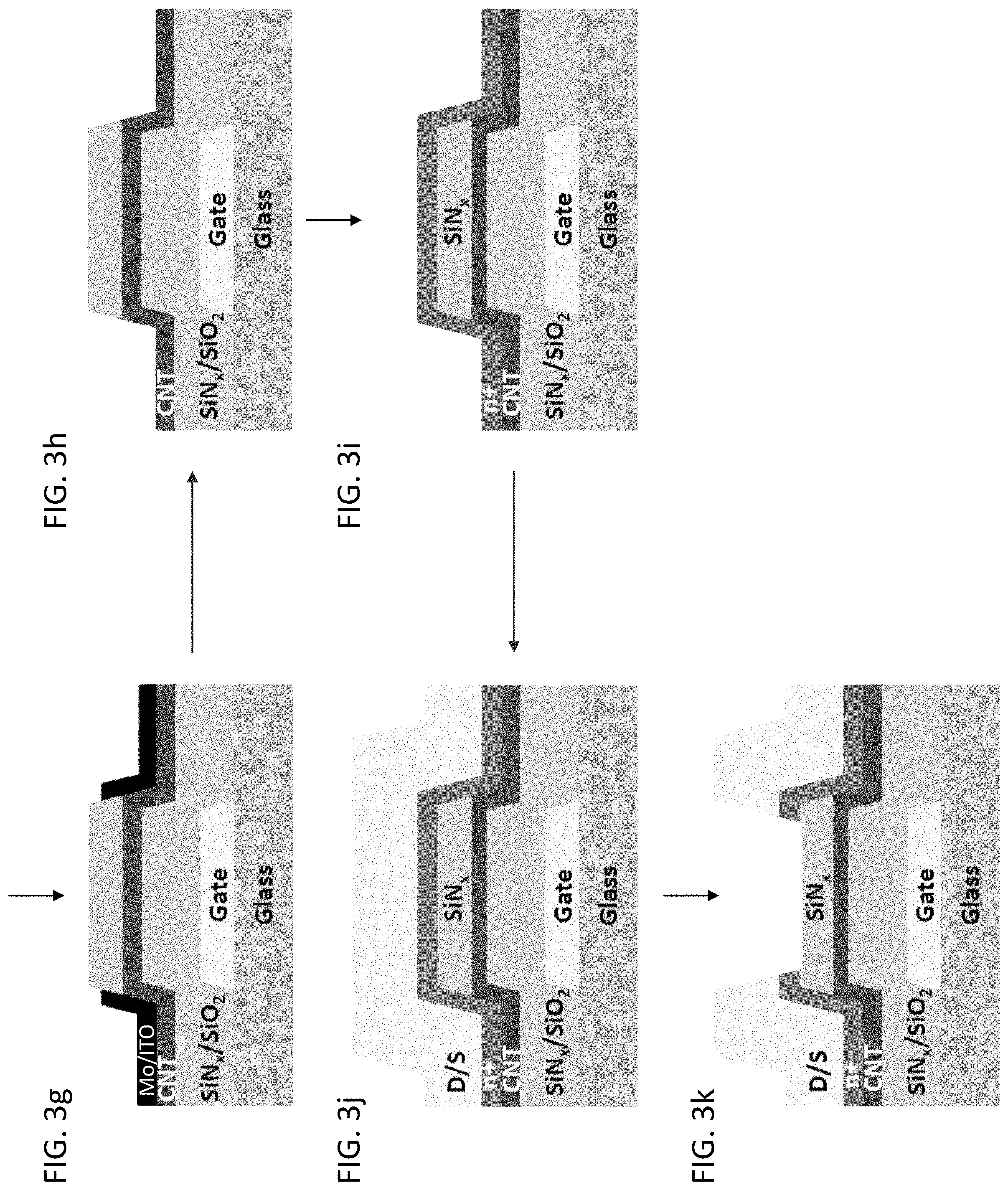
[0098] Although many processes may be used to form such CNF TFTs, including specifically bottom gated etch-stop CNT TFTs, many such embodiments use a process as summarized in FIGS. 3a to 3k and described below. As shown, the method requires a number of process steps into which the CNT layers are integrated. These steps include: [0099] The provision of a substrate and the formation atop the substrate of a patterned gate electrode (FIG. 3a). [0100] The deposition of a gate electrode dielectric atop the gate electrode layer (FIG. 3b). [0101] The deposition of a CNT thin film back-layer atop the dielectric layer (FIG. 3c). [0102] The deposition of a CNT protection layer atop the CNT thin film back-layer (FIG. 3d). [0103] The patterning of the CNT protection layer to expose the portion of the CNT back-layer above the gate electrode, leaving at least the edges with the CNT thin film covered by the CNT protection layer (FIG. 3e). [0104] The deposition of an etch stopper dielectric layer atop the exposed portion of the CNT thin film and remaining CNT protection layer (FIG. 3f). [0105] The patterning and etching of the etch stopper dielectric layer to deposit a second dielectric layer selectively atop the portion of the CNT thin film above the gate electrode (FIG. 3g). [0106] The removing of the remaining CNT protection layer to expose the CNT thin film on the edges of the gate electrode channel (FIG. 3h). [0107] The deposition of an n+ doped layer atop the CNT thin film and the etch stop dielectric layer (FIG. 3i). [0108] The deposition of the drain/source electrode layer atop the n+ doped layer (FIG. 3j). [0109] The patterning and etching of the drain/source electrodes (FIG. 3k).
[0110] The processing of such an etch-stop (ES) CNT TFT requires a few additional deposition steps, however it can be advantageous in some respects because it has the etch-stop layer that protects the back-channel so the intrinsic layer can remain thin (e.g., less than .about.200 nm). Despite the above description it will be understood that the CNT back-channel layers can also be combined with other structures and techniques, including, for example back-channel-etched (BCE) TFTs. An exemplary process for such a BCE TFT is provided in FIGS. 4a to 4f, and described below. These steps include: [0111] The provision of a substrate and the formation atop the substrate of a patterned gate electrode (FIG. 4a). [0112] The deposition of a gate electrode dielectric atop the gate electrode layer (FIG. 4b). [0113] The deposition of both drain/source electrode and n+ doped layers atop the dielectric layer (FIG. 4c). [0114] The patterning and etching of the drain/source electrodes and the n+ layer (FIG. 4d). [0115] The deposition of a CNT thin film back-layer atop the n+ layer (FIG. 4e). [0116] The deposition of a passivation layer atop the CNT thin film back-layer (FIG. 4f).
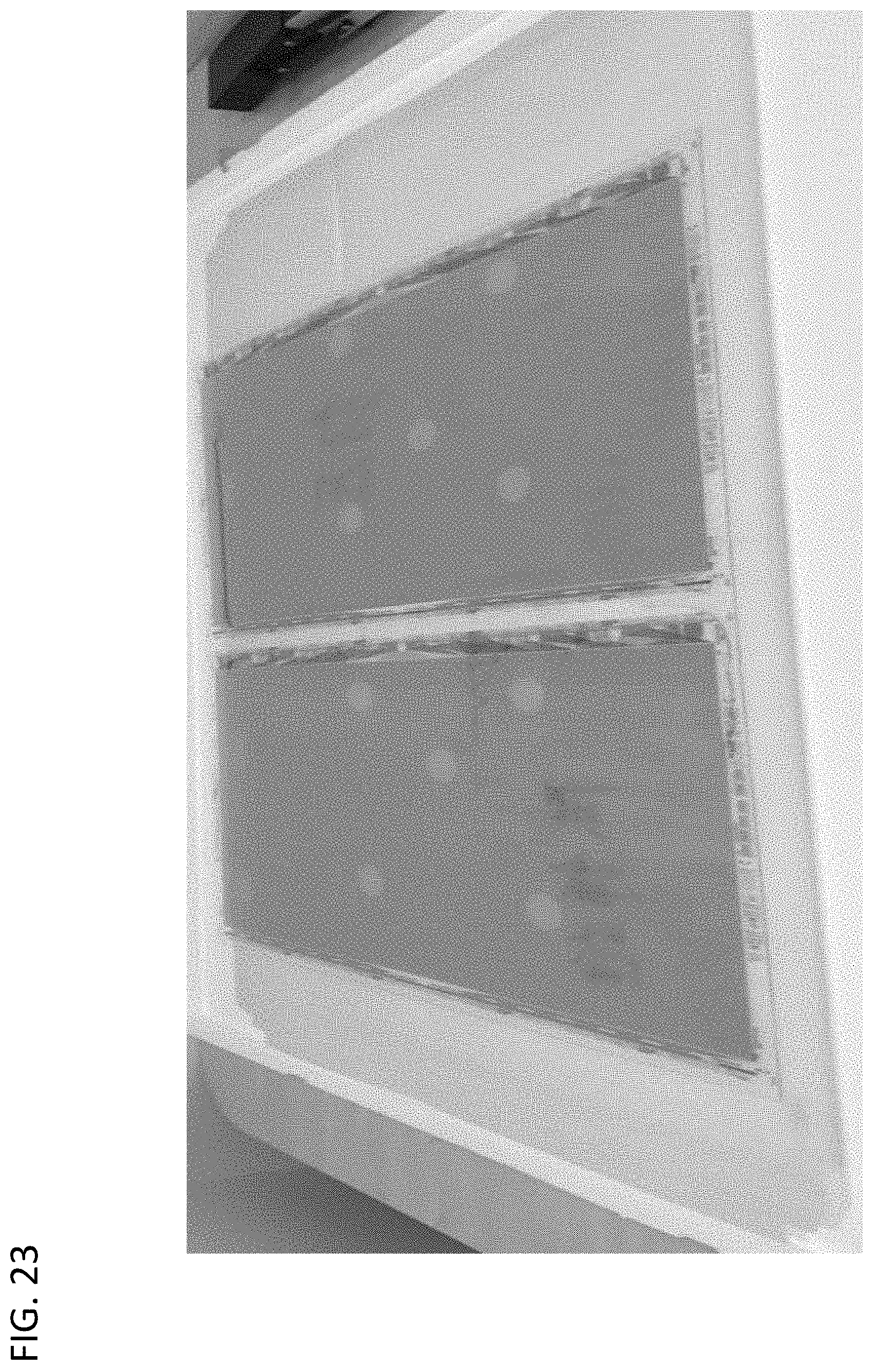
[0117] Although the above methods are described in FIGS. 3 and 4 with respect to specific deposition techniques, it should be understood that many alternative embodiments and techniques may be used in association with the CNT back-layers in accordance with embodiments.
[0118] For example, in some such embodiments, as shown in FIGS. 3a and 4a, a substrate is provided onto which a gate electrode is formed. Although the substrate in the figures is listed as being glass, it should be understood that any material having sufficient optical transmission (e.g., in many embodiments, on the order of 80% or greater), and capable of resisting degradation at industrial standard processing temperatures (e.g., 100.degree. C. and higher) may be used. Exemplary substrate material may include glass, polyethylene terephthalate (PET), polyethesulphone (PES), palyarylate (PAR), and polycarbonate (PA), among others. Similarly, the gate electrode itself may be made of any suitable metal such as Cu, Al, Ag, Mo, Cr, Nd, Ni, Mn, Ti, Ta or W, or the alloy of two or more of these metals. The gate metal layer may be in a single layer structure or a multi-layer structure, and the multi-layer structure may be of, for example Cu\Mo, Ti\Cu\Ti, Mo\Al\Mo or etc. The thickness of the gate electrode may be any suitable size, such as from 10 nm to more than 100 .mu.m, and in some embodiments around 400 nm, as shown in FIGS. 3a and 4a.
[0119] Likewise, although the process for depositing the gate electrode is listed as comprising the steps of sputtering and patterning, it should be understood that many suitable and standard industrial processes may be use to pattern and deposit gate electrodes atop the substrate. For example, sputtering (or physical vapor deposition) may include one or a combination of electronic, potential, etching and chemical sputtering, among others. Deposition techniques may alternatively include, for example, chemical (CVD), plasma-enhanced vapor deposition (PECVD), and/or thermal evaporation, etc.
[0120] Similarly, the patterning of the underlying gate electrode may incorporate any suitable photoengraving process, such as wet or dry etching, including the utilization of any suitable photoresist and etching chemicals. In many such embodiments the gate electrode layer may be coated with a layer of a suitable photoresist, the photoresist may then be exposed and developed by the mask plate to respectively form a photoresist unreserved area and a photoresist reserved area. In many such embodiments the photoresist reserved area corresponds to an area where the gate electrode is arranged, and the photoresist unreserved area corresponds to other areas. In such embodiments the gate metal layer of the photoresist unreserved area may be completely etched off by the etching process, and the remaining photoresist removed, so that the gate electrode is formed.
[0121] Once the gate electrode is formed, as shown in FIGS. 3b and 4b, a suitable dielectric layer is formed atop the substrate and gate electrode layer. Again, although a PECVD process and a SiN dielectric material is specified in the figures, it should be understood that any suitable dielectric material and deposition process may be incorporated with methods. For example, in many embodiments the dielectric layer may be made of inorganic and organic materials, an oxide, a nitride, or a nitrogen oxide, such as, for example, SiNx, SiOx, TaOx, AlOx, or Si(ON)x. Moreover, the dielectric layer may be in a single layer structure, a dual layer structure or a multi-layer structure. The thicknesses of such structures may be take any size suitable to provide the dielectric function. In addition, the dielectric layer may be formed atop the substrate and gate electrode by any suitable the filming process, including, for example, magnetron sputtering, thermal evaporation, CVD (remote plasma, photo catalytic, etc.), PECVD, spin coating, liquid phase growth, etc. In various such embodiments, as shown in FIGS. 3b and 4b, the CNT TFTs incorporate SiN.sub.x/SiO.sub.2 layers deposited via PECVD at thicknesses of around 200 nm. Finally, if necessary a variety of feedstock gas molecules may be made in association with such dielectric materials, including SiHx, NH.sub.x, N.sub.2, and hydrogen free radical and ions. Similar techniques and materials may be used for the other passivation layers, including those etch-stop layers formed in FIG. 3f and the passivation layer shown in FIG. 4f. In these steps the deposit temperatures and thicknesses of the passivation materials may be chosen as required.
[0122] Regardless of whether the TFT is an ES or BEC TFT, all TFTs also require the deposition of n+ and drain/source layers, as shown in FIGS. 3i & 3j, and 4c. Although the figures show that sputter deposition of an approximately 400 nm Mo drain/source layer, and PECVD deposition of a thin (.about.10 nm) n+ doped layer, it should be understood that any suitable combination of deposition techniques and materials may be utilized. For example, the drain/source electrode layer may be made of any suitable metal such as Cu, Al, Ag, Mo, Cr, Nd, Ni, Mn, Ti, Ta or W, or the alloy of two or more of these metals. The gate metal layer may be in a single layer structure or a multi-layer structure, and the multi-layer structure may be of, for example Cu\Mo, Ti\Cu\Ti, Mo\Al\Mo or etc. The thickness of the gate electrode may be similarly be of any suitable size, such as from 10 nm to more than 100 .mu.m, and in some embodiments around 400 nm, as shown in the figures. Likewise, although the process for depositing the electrode is listed as comprising the steps of sputtering and patterning, it should be understood that many suitable and standard industrial processes may be use to pattern and deposit gate electrodes atop the substrate. For example, sputtering (or physical vapor deposition) may include one or a combination of electronic, potential, etching and chemical sputtering, among others. Deposition techniques may alternatively include, for example, chemical (CVD), plasma-enhanced vapor deposition (PECVD), and/or thermal evaporation, etc.
[0123] Similarly, any suitable n+ material may be incorporated into the TFTs in accordance with embodiments, include, for example, n+ doped amorphous Si, or other suitable semiconductors including arsenide and phosphides of gallium, and telluride and sulfides of cadmium. Likewise and suitable plasma and/or n-type doping materials may be used with such semiconductors, including, for example, phosphorous, arsenic, antimony, bismuth, lithium, beryllium, zinc, chromium, germanium, magnesium, tin, lithium, and sodium, for example. And, these materials may be deposited with any suitable deposition technique including, thermal, physical, plasma, and chemical vapor deposition techniques, as described above. Some suitable techniques include, for example, aerosol assisted CVD, direct liquid injection CVD, microwave plasma-assisted CVD, atomic layer CVD, combustion chemical vapor deposition, hot filament CVD, hybrid physical-chemical vapor deposition, rapid thermal CVD, vapor-phase epitaxy and photo-initiated CVD. Alternatively, atomic layer deposition might be substituted for CVD for the thinner and more precise layers.
[0124] A number of steps in such processes also require the patterning and etching of materials (see, e.g., 3e, 3h, 3k and 4d). In such processes any suitable patterning and etching technique may be incorporated with embodiments. In particular, many of the steps incorporate a patterning process by which a passivation layer is deposited and a pattern is formed through the passivation layer. Specifically, in many embodiments the passivation layer may be coated with a layer of any suitable photoresist. In such embodiments the photoresist may be exposed and developed by a mask plate to respectively form a photoresist unreserved area and a photoresist reserved area. For example, the photoresist of the unreserved area may correspond in various embodiments to an area where the via hole of the passivation layer is arranged.
[0125] Any suitable optical photolithographic technique may be used, including for example, immersion lithography, dual-tone resist and multiple patterning electron beam lithography, X-ray lithography, extreme ultraviolet lithography, ion projection lithography, extreme ultraviolet lithography, nanoimprint lithography, dip-pen nanolithography, chemical lithography, soft lithography and magneto lithography, among others.
[0126] Regardless of the specific techniques and light source used, such lithographic techniques generally incorporate several steps. In many embodiments, the layer to be patterned is first coated with a photoresist, such as by spin coating. In such techniques, a viscous, liquid solution of photoresist is dispensed onto the wafer, and the wafer is spun rapidly to produce a uniformly thick layer. The spin coating typically runs at 1200 to 4800 rpm for 30 to 60 seconds, and produces a layer between 0.5 and 2.5 micrometers thick. The spin coating process results in a uniform thin layer, usually with uniformity of within 5 to 10 nanometers, or more. In various embodiments, the photo resist-coated material may then be prebaked to drive off excess photoresist solvent, typically at 90 to 100.degree. C. for 30 to 60 seconds on a hotplate. After the non masked portions of the layer are etched, either by a liquid ("wet") or plasma ("dry") chemical agent to remove the uppermost layer of the substrate in the areas that are not protected by photoresist. After a photoresist is no longer needed, it is then removed from the substrate. This photoresist may be removed chemically or by a plasma or by heating.
[0127] Although specific deposition and patterning methods are disclosed, as well as specific materials for substrates, electrodes, dielectrics, passivation layers, etc., and specific conditions, including, thicknesses, temperatures etc., it will be understood that any of these parameters may be adjusted as necessary for the specific TFT configuration and operational parameters without fundamentally altering the principles of embodiments that incorporate the CNTs disclosed herein.
Embodiments Implementing SWCNT Deposition Techniques
[0128] Turning to embodiments of methods for depositing the CNT layers in the TFTs, in many embodiments various techniques may be used, including various depositions and spraying methods.
[0129] In many embodiments, single-walled carbon nanotube thin films are solution coated using a spraying technique, such as air, aerosol or ultrasonic spraying in association with a moving station manufacturing line, as described in relation to FIGS. 5a to 5c. As shown in FIG. 5a, in many embodiments a moving station is provided onto which substrates are loaded, and in association with a carbon nanotube solution may be sprayed (e.g., by aerosol or air spray coating) onto the substrates of a suitable size (e.g., 4''-100'') while heating them at a desirable processing temperature (e.g., from 60-200.degree. C., or any temperature that is allows by the underlying materials and the CNT materials themselves). In such embodiments, the moving speed of station may be controlled to keep the film thickness and uniformity (e.g., 1 mm/s-1000 mm/s).
[0130] In other embodiments, ultrasonic spray coating may be used. As shown in FIG. 5b, in such embodiments a stream of compressed air is passed through an aspirator, which creates a local reduction in air pressure that allows the carbon nanotube solution to be pulled out from a container at normal atmospheric pressure. During processing, the ultrasonicating nozzle atomizes the carbon nanotube solution into very tiny droplets of, for example, anywhere from a few pm to around 1000 .mu.m in diameter. The tiny droplets are then deposited onto substrates at a suitable processing temperature (e.g., up to 400.degree. C.), such that the droplets are immediately dried to mitigate the O-ring aggregations. In various embodiments, a temperature of 100.degree. C. may be used. Although any suitable air pressure may be used (dependent on the viscosity of the material, in many embodiments the compressed air pressure can be ranged from 20 psi (1.38 bar) to 100 psi (6.8 bar) dependent upon the solution viscosity and the size of aspirator required for the deposition.
[0131] In embodiments incorporating aerosol spray coating (as shown in FIG. 5c), the carbon nanotube solution may be atomized using high pressure gas (e.g., 200-1000 standard cubic centimeter per minute (sccm)), or ultra-sonication (e.g., 20 V-48 V, 10-100 Watts) to produce 1-5 micron aerosols that are brought to spray head by carrier gas (e.g., 10-30 sccm). It should be understood that these processing parameters are only exemplary and that other deposition properties may be used dependent on the type of material, the nature of aerosols desired and the thickness of the coatings to be formed.
[0132] FIGS. 6 and 7 shown images of thin films of SWCNT spray coated onto substrates using an airbrush technique (FIG. 6) and using an aerosol technique (FIG. 7), according to embodiments. In many embodiments, thus formed carbon nanotube thin films are treated by acetic acid gas generated by airbrush spray or aerosol spray and then washed with isopropanol to achieve clear carbon nanotube surfaces. The clear carbon nanotube surfaces are characterized with atomic force microscope (AFM). These samples could not be characterized on glass substrate using scanning electron microscope due to the highly insulation of such substrates. As shown, FIG. 8 provides an AFM image of airbrush sprayed SWCNT thin film, and FIG. 9 provides an AFM image of aerosol sprayed SWCNT thin film. This imagery provides proof of the robust nature of the deposition process, and the ability to depose high quality thin film coatings of SWCNT.
[0133] In embodiments, carbon nanotube thin films formed in accordance with such spray coating processes are used to replace amorphous silicon in 4-photomask photolithography processes to pattern drain/source electrodes, dielectrics, top-gated electrodes, and pixel electrodes following industry manufacturing standard methods, as described above with respect to FIGS. 3 and 4.
[0134] Although the embodiments shown in FIGS. 3 and 4 are shown as extending beyond the channel, in order to reduce the subthreshold current leakage, other embodiments may employ at least one additional photomask to pattern the active carbon nanotube thin layer using photolithography. In such embodiments, the CNT layer outside of the transistor channels may be removed by a suitable etching technique, such as, for example, O.sub.2 plasma or wet etching. In various such embodiments, the clear uniform carbon nanotube thin film may be photoresist (PR) coated and photo exposed, and then solution developed. On these developed areas, the carbon nanotube thin film is etched using, for example, O.sub.2 plasma or a wet chemical etching, such as a buffered HF solution. The undeveloped PR is then stripped off to leave a patterned carbon nanotube thin film. A flow-chart providing one embodiment of such a method is provided in FIG. 10. It should be understood that any of the steps and techniques listed in the flow-chart may be substituted with alternatives as described in detail above.
[0135] In still other embodiments, to reduce the use of an extra photomask to pattern active carbon nanotubes and to reduce the consumption of the carbon nanotube solution, the SWCNT thin films may be printed atop the substrate. In many such embodiments, an aerosol jet printer may be used to print the active carbon nanotube thin film using small nozzle size (e.g., <100 .mu.m). An aerosol jet printer can deposit <10 .mu.m linewidth with <2 .mu.m registration accuracy. To do so, the aerosol jet printer prints carbon nanotubes on patterned drain/source marks. An image of such an aerosol printing set-up is provided in FIG. 11. FIG. 12 shows photo and optic images of exemplary drain/source marks before printing SWCNT films. FIG. 13 provides photo image and optic images of printed SWCNT thin film on drain/source marks. As described above, aerosol jet printed carbon nanotubes can be treated with aerosol sprayed or airbrush sprayed acetic acid gas, and followed by isopropanol washing. These clear carbon nanotube thin films can then be characterized with SEM. The SEM image (FIG. 14) displays clear carbon nanotube films on drain/source markers, in accordance with embodiments. The clear carbon nanotube films have been characterized with a Keithly 4200 semiconductor characterization system to show semiconducting properties, as shown in FIGS. 15a-15c.
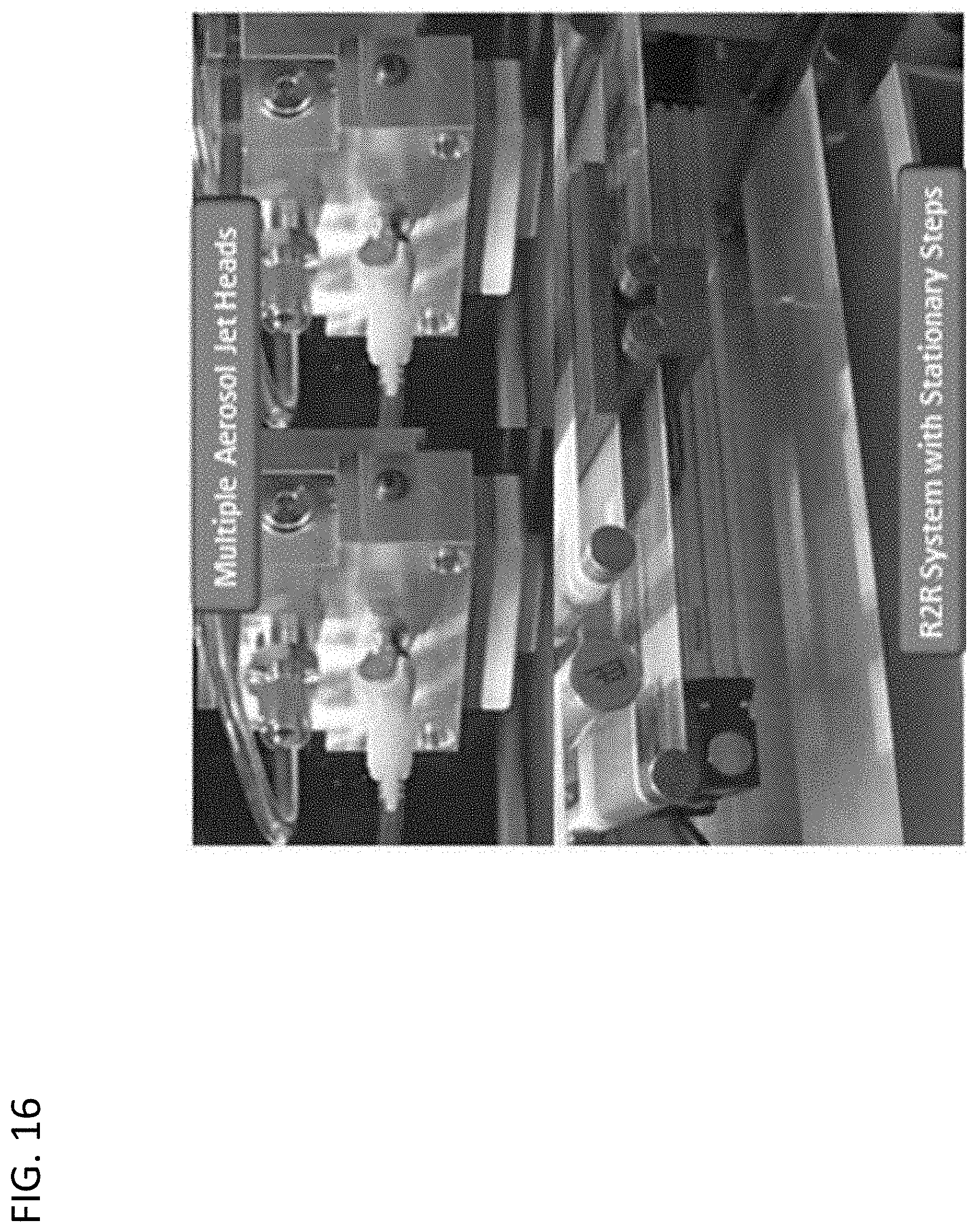
[0136] To further take advantage of low-cost, low environmental impact and large area fabrication due to the small number of process steps, limited amount of material and high through-put, embodiments propose to aerosol jet printing methods described above (including its high precision: registration accuracy of 1-2 .mu.m) with a roll-to-roll system with high speed process. With such a roll-to-roll aerosol jet printer, SWCNT ink can be printed in a rapid way for mass production in a-Si TFT backplane manufacturing line. Also, fully printed SWCNT TFT backplanes can be fabricated massively using roll-to-roll system. To match up with industry speed, embodiments disclose multiple aerosol jet printer heads mounted on moving station, such as shown in FIG. 16, may be used for high speed printing carbon nanotube thin films. On a moving station, such multiple aerosol jet printer heads can print a large number of carbon nanotube patterns.
Exemplary Embodiments
[0137] Additional embodiments and features have been set forth in part in the exemplary embodiments below, and in part will become apparent to those skilled in the art upon examination of the specification or may be learned by the practice of the invention. None of the specific embodiments are proposed to limit the scope of the remaining portions of the specification and the drawings, and they are provided as exemplary of the devices, methods and materials disclosed herein. In particular, although specific structures and particular combinations of materials are recited, it should be understood that these are merely provided as examples, and any suitable alternative architectures and materials may be substituted.
EXAMPLE 1
Comparison of Conventional a-Si TFT and CNT TFT Techniques
[0138] A flow-chart for an exemplary method for manufacturing an amorphous silicon TFT backplane on manufacturing lines is provided in FIG. 17. As shown in this method amorphous Si is deposited over large areas by plasma enhanced chemical vapor deposition, and then other devices are fabricated following other conventional manufacturing steps. In embodiments the amorphous silicon may be replaced by CNTs. Such CNT films may be deposited and/or printed in accordance with techniques previously described. Using such clear carbon nanotube thin films according to embodiments, standard industry manufacturing methods may be used to further pattern drain/source electrodes, dielectrics, top-gated electrodes and pixel electrodes as described in FIGS. 18 and/or 19.
EXAMPLE 2
SWCNT TFTs
[0139] Using the techniques described above it is possible to formed single-walled carbon nanotube thin film transistor, as shown, for example, in FIG. 20.
EXAMPLE 3
Displays
[0140] Finally, although the above exemplary embodiments and discussion have focused on methods, architectures and structures for individual devices and backplanes, it will be understood that the same architectures and structures may be combined as pixels into a display device. In such an embodiment, a plurality of SWCNT TFTs as described herein may be combined and interconnected as is well-known by those skilled in the art, such as by electronically coupling the devices into addressing electrode lines, to form a TFT-backplane for a display, such as an AMOLED display.
EXAMPLE 4
Industrially Robust Carbon Nanotube TFTs
[0141] Results of studies on exemplary embodiments of systems and methods for the industrial manufacturing of carbon nanotube thin film transistors and products formed from such systems and methods are provided. These embodiments demonstrate that such systems and methods produce carbon nanotubes at 1100.degree. C. and 10 atmosphere pressure. Various such carbon nanotube embodiments are capable of withstanding sputter processes, distinguishing them from conventional chemical vapor deposited carbon nanotubes. Embodiments demonstrate that that electronically pure semiconducting carbon nanotubes produced according to embodiments can be configured to fully replace amorphous silicon for display backplanes.
[0142] In contrast to current a-Si, LTPS and oxide TFTs, electronically pure SWCNT TFTs exhibit equivalent or better figures of merit for a number of important characteristics, including, high field effect mobility, low temperature fabrication, good stability, uniformity, scalability, flexibility, transparency, mechanical deformability, low voltage and low power, bendability and low cost. Recently, Hennrich et al. reported aligned semiconducting carbon nanotube transistors exhibited a hole mobility of about 300 cm.sup.2/Vs and 108 ON/OFF ratio. (See, e.g., F. Hennrich, et al., ACS Nano, vol. 10, pp. 1888-1895, 2016, the disclosure of which is incorporated herein by reference.) Meanwhile, Bao's group at Stanford demonstrated stretchable carbon nanotube transistors characteristics of 15 cm.sup.2/Vs and .about.103 ON/OFF ratio based on elastomer substrate and elastomer dielectrics. (See, e.g., A. Chortos, et al., ACS Nano, vol. 11, pp. 7925-7937, 2017, the disclosure of which is incorporated herein by reference.) Despite the potential promise of these materials, industrial concerns exist about the adoptability of current bench mark manufacturing lines for the fabrication of carbon nanotube thin film transistors. Embodiments herein are directed to systems and methods for the production of carbon nanotube thin film transistors under stringent industrial conditions. Carbon nanotube thin film transistors according to embodiments realize: cost saving, improved quality, a capability to implement flexible and wearable displays, and capability to replace current amorphous silicon backplanes.
[0143] Although many methods for each of these processes are known in the art, it has been determined that forming carbon nanotube thin films capable of being integrated into thin film transistors under standard industrial conditions requires a set of particular processes and conditions. Specifically, in order for carbon nanotube thin film transistors to be produced and integrated into an industrial manufacturing line according to embodiments several key points need to be considered: 1) the adhesion of carbon nanotube thin films to the substrates; 2) the fidelity of the solution process on large size substrates up to Gen10.5 line using carbon nanotube aqueous ink; 3) the industrial wet etch conditions necessary to prevent damage to the carbon nanotube thin films; and 4) the PECVD growth conditions necessary to integrated carbon nanotube thin films within the overall thin film transistor devices. Using embodiments of methods and processes as described herein carbon nanotube thin films are demonstrated capable of forming thin film transistors robust to industrial conditions.
[0144] As shown in FIGS. 21a to 21c, in many embodiments methods are capable of producing amorphous silicon like carbon nanotube thin film transistors using amorphous silicon nitride as dielectrics on glass substrates. Moreover, embodiments of carbon nanotube thing film transistors demonstrate stress stability under 10 V gate for 2000 second (10 second per cycle), thermal stability, and photostability (e.g., FIGS. 22a to 22c). Embodiments further demonstrate that carbon nanotube thin film transistors according to processes and methods can be completely produced in currently benchmark display backplane manufacturing lines with cost-saving.
[0145] First, studies conducted on carbon nanotube thin films according to embodiments demonstrate that they stick to suitable substrates through hydrophobicity forces. The peel off force is estimated to be at least 4.35 N/cm.sup.2. (See, e.g., S. V. Aradhya, et al., Journal of The Electrochemical Society, vol. 155, pp. K161-K165, 2008, the disclosure of which is incorporated herein by reference.) Accordingly, carbon nanotube thin films will not peel off from substrates and consequently pollute manufacturing lines, as previously considered a potential problem.
[0146] In order to demonstrate the ability of embodiments of solution processes with aqueous carbon nanotube ink to operate on an industrial scale, a carbon nanotube solution was deposited on 20 pieces of Gen 4.5 glass substrate at ambient environment (see, e.g., FIG. 23). Accordingly, these studies demonstrate that embodiments can be expanded to large size glass substrates such as Gen 10.5 glasses. Importantly, this is the first demonstration of a real solution process for thin film transistors. Therefore, embodiments make it possible to save display manufacturers tremendous costs in high temperature and high vacuum evaporation of semiconducting materials such as silicon, metal oxides. This solution process can be further explored in printing systems, as previously described.
[0147] Different from small scale lift-off photolithography, display manufacturers commonly utilize acids to wet etch metals for electrode patterning. The conventional view is that utilizing such etch methods may result in the removal of carbon nanotubes by acid etching. To demonstrate the robust nature of current embodiments of systems and methods for manufacturing using amorphous silicon thin film transistors Alumina was evaporated on carbon nanotube thin films. After photoresist coating and developing, the substrate was immersed in 55% H.sub.3PO.sub.4, 15% HNO.sub.3, 5% Acetic Acid and water. The patterned Al electrodes were probed on Keithley 4200 semiconductor characterization system to show perfect connection (as shown in FIG. 24). This result is consistent with wet-etching copper covered carbon nanotubes using a commercial copper etchant ferric chloride. (See, e.g., A. Chortos, et al., Advanced Materials, vol. 28, pp. 4441-4448, 2016, the disclosure of which is incorporated herein by reference.) These results strongly demonstrated that metal etchants including acids have negligible effects on carbon nanotube thin films.
[0148] Embodiments also demonstrate the importance of the PECVD growth conditions for the dielectric materials (e.g., SiNx) to ensure the performance of the amorphous silicon like carbon nanotube thin film transistors described herein. In such embodiments SiN.sub.x plays two roles: a first role is to be a dielectric for charge carrier modulation in semiconducting carbon nanotube thin films; and second role is to dope carbon nanotube thin films to form n-type semiconductor. This doping process could also effect the contacts between metal electrode and carbon nanotube thin films. With different PECVD systems, it shown to be necessary to adjust the feed gas, temperature, pressure and stress conditions. Examples are provided in Table 1, below. In a first example, a Unaxis 790 PECVD was used for SiN.sub.x growth and it was found that the best deposition parameters require a flow rate of ammonium to silane in the ratio of 10 sccm/5.3 sccm. (See, e.g., H. Li, et al., ACS Applied Materials & Interfaces, vol. 8, pp. 20527-20533, 2016; and H. Li, ECS Journal of Solid State Science and Technology vol. 5, pp. M93-M98, 2016, the disclosures of which are incorporated herein by reference.) Using the same flow rate of NH.sub.3 to SiH.sub.4 with STS PECVD, no current was detected, indicating damage of the carbon nanotube thin films. However, with an STS PECVD recipe, the fabricated carbon nanotube thin film transistors showing the similar characteristics as presented in FIG. 25.
TABLE-US-00001 TABLE 1 Deposition Parameters N.sub.2 (sccm) He (sccm) NH.sub.3 (sccm) SiH.sub.4LF (sccm) Pwr (W) P (mTorr) T (.degree. C.) Unaxis 790 PECVD 100 400 10 5.3 40 900 225 STS PECVD 1960 0 40 43 80 500 250-280
[0149] These combination of results demonstrate that embodiments may be used by display manufacturers to produce carbon nanotube thin film transistors using current bench mark thin film transistor backplane manufacturing lines. These results can be an important impetus for using carbon nanotube thin film transistors to replace amorphous silicon for display industrial, especially for emerging flexible and wearable displays.
Doctrine of Equivalents
[0150] Having described several embodiments, it will be recognized by those skilled in the art that various modifications, alternative constructions, and equivalents may be used without departing from the spirit of the invention. Additionally, a number of well-known processes and elements have not been described in order to avoid unnecessarily obscuring the present invention. Accordingly, the above description should not be taken as limiting the scope of the invention.
[0151] Those skilled in the art will appreciate that the presently disclosed embodiments teach by way of example and not by limitation. Therefore, the matter contained in the above description or shown in the accompanying drawings should be interpreted as illustrative and not in a limiting sense. The following claims are intended to cover all generic and specific features described herein, as well as all statements of the scope of the present method and system, which, as a matter of language, might be said to fall there between.
* * * * *
D00000
D00001
D00002
D00003
D00004
D00005
D00006
D00007
D00008
D00009
D00010
D00011
D00012
D00013
D00014
D00015
D00016
D00017

D00018
D00019
D00020

D00021
D00022
D00023
D00024
D00025
D00026
XML
uspto.report is an independent third-party trademark research tool that is not affiliated, endorsed, or sponsored by the United States Patent and Trademark Office (USPTO) or any other governmental organization. The information provided by uspto.report is based on publicly available data at the time of writing and is intended for informational purposes only.
While we strive to provide accurate and up-to-date information, we do not guarantee the accuracy, completeness, reliability, or suitability of the information displayed on this site. The use of this site is at your own risk. Any reliance you place on such information is therefore strictly at your own risk.
All official trademark data, including owner information, should be verified by visiting the official USPTO website at www.uspto.gov. This site is not intended to replace professional legal advice and should not be used as a substitute for consulting with a legal professional who is knowledgeable about trademark law.