Multiple Memory States Device And Method Of Making Same
DUMITRU; Viorel-Georgel ; et al.
U.S. patent application number 16/659608 was filed with the patent office on 2020-04-23 for multiple memory states device and method of making same. This patent application is currently assigned to CYBERSWARM, INC.. The applicant listed for this patent is CYBERSWARM, INC.. Invention is credited to Cristina BESLEAGA STAN, Viorel-Georgel DUMITRU, Aurelian-Catalin GALCA, Alin VELEA.
| Application Number | 20200126614 16/659608 |
| Document ID | / |
| Family ID | 70279696 |
| Filed Date | 2020-04-23 |
| United States Patent Application | 20200126614 |
| Kind Code | A1 |
| DUMITRU; Viorel-Georgel ; et al. | April 23, 2020 |
MULTIPLE MEMORY STATES DEVICE AND METHOD OF MAKING SAME
Abstract
A phase-change material based resistive memory contains a resistive layer and two electrical contacts. After fabrication the memory is subjected to thermal treatment which initiates a transition toward a crystalline state favoring in this way the subsequent obtaining of a large number of resistive memory states.
| Inventors: | DUMITRU; Viorel-Georgel; (Ploiesti, RO) ; BESLEAGA STAN; Cristina; (Bucharest, RO) ; VELEA; Alin; (Bucharest, RO) ; GALCA; Aurelian-Catalin; (Magurele, RO) | ||||||||||
| Applicant: |
|
||||||||||
|---|---|---|---|---|---|---|---|---|---|---|---|
| Assignee: | CYBERSWARM, INC. Ploiesti RO |
||||||||||
| Family ID: | 70279696 | ||||||||||
| Appl. No.: | 16/659608 | ||||||||||
| Filed: | October 22, 2019 |
Related U.S. Patent Documents
| Application Number | Filing Date | Patent Number | ||
|---|---|---|---|---|
| 62749426 | Oct 23, 2018 | |||
| Current U.S. Class: | 1/1 |
| Current CPC Class: | H01L 45/144 20130101; H01L 45/126 20130101; G11C 2013/005 20130101; H01L 45/1233 20130101; H01L 45/1226 20130101; G11C 13/004 20130101; H01L 45/1641 20130101; G11C 13/0069 20130101; G11C 13/0004 20130101; G11C 2013/0092 20130101; G11C 11/5678 20130101; H01L 27/2463 20130101; H01L 45/06 20130101; G11C 2013/0045 20130101; H01L 45/1675 20130101; H01L 45/1625 20130101 |
| International Class: | G11C 11/56 20060101 G11C011/56; H01L 27/24 20060101 H01L027/24; H01L 45/00 20060101 H01L045/00; G11C 13/00 20060101 G11C013/00 |
Claims
1. A phase-change material based resistive memory containing: a resistive layer; two electrical contacts and which is subjected after fabrication to a specific thermal treatment, which initiates its transition toward the crystalline state favoring in this way the subsequent obtaining of a large number of resistive memory states.
2. A phase-change material based resistive memory like described in claim 1 that has a planar structure, with the PCM resistor and the two electrical contacts situated in the same plane on the substrate surface.
3. A phase-change material based resistive memory like described in claim 1 that has a vertical structure, with the two contacts placed below and above the PCM layer.
4. A phase-change material based resistive memory like described in claim 1 where the PCM layer is a Ge--Te layer.
5. A phase-change material based resistive memory like described in claim 1 where the specific thermal treatment is performed in air atmosphere at a temperature in between 190 C-210 C.
6. A phase-change material based resistive memory like described in claim 1 which afterwards could be set to a large number of different resistive states by applying voltage pulses with different amplitudes.
7. A phase-change material based resistive memory like described in claim 1 which afterwards could be set to a large number of different resistive states by performing voltage sweeps with different upper limits.
8. A method for obtaining a multiple states resistive memory based on phase-change materials and consisting in: deposition of PCM resistor and of the two electrical contacts annealing the fabricated PCM resistor in inert atmosphere at a temperature between 190 C-210 C in order to initiate its transition toward the crystalline state obtain subsequently multiple resistive states by applying certain voltage signals.
9. A method like described in claim 8 where the certain voltage signals are voltage pulses with different amplitudes.
10. A method like described in claim 8 where the certain voltage signals are voltage sweeps with different upper limits.
Description
CROSS REFERENCE OF RELATED APPLICATION
[0001] This application claims the benefit of U.S. Provisional Patent Application No. 62/749,426, filed Oct. 23, 2018, which is incorporated by reference in its entirety.
BACKGROUND
[0002] Resistive memories are devices that can store information as different resistive states. For increasing memory density and data capacity, it is highly desirable to have a resistive memory with multiple resistive states. Resistive memories with multiple states may be used in many applications like non-volatile solid state memories, programmable logic, pattern recognition, neuromorphic computing, etc.
[0003] Among resistive memories with multiple memory states, those based on phase-change materials (PCM) such as chalcogenides are promising. PCM based resistive memories (also referred to as PCM memristors) may exhibit a reversible structural phase change between an amorphous (highly resistive) state and a crystalline (highly conductive) state. The switching between the two states (the amorphous state and the crystalline state) may be achieved by applying pulses (e.g., current pulses, voltage pulses, etc.) with different characteristics. The conductive state may be obtained by applying a longer but lower amplitude pulse which may locally heat the amorphous region and may lead to crystallization, whereas the insulating state may be obtained by applying a shorter but higher amplitude pulse which may lead to local melting and the formation of an amorphous region by rapid quenching. In applications as a resistive memory, the pronounced difference in electrical resistivity of PCM may be used.
[0004] To achieve multiple memory states, multiple intermediary resistive states may be needed. An example solution for achieving multiple intermediary resistive states is described in U.S. Pat. No. 8,116,115B2 and references therein. This solution is based on controlling the duration, amplitude and shapes of the pulses (e.g., voltage or current pulses). Another example solution is described in U.S. Pat. No. 6,087,674. This solution is based on building a memory element such that it contains a heterogeneous mixture of a phase-change material and a dielectric material and providing a way to deliver the electrical pulses only to a portion of the memory material volume. However, the existing solutions for achieving the multiple resistive states are either complicated from a fabrication point of view or are difficult to control.
SUMMARY
[0005] The present disclosure is directed toward a nonvolatile, resistive memory with multiple resistive states based on PCM and a method of making the same. The resistive memory may include a substrate, a PCM layer and two electrical contacts. In one embodiment, the device may have a planar structure. In another embodiment, the device may have a vertical structure with the two electrical contacts placed below and above the PCM layer. The PCM layer may be deposited by magnetron sputtering in an amorphous, high resistive state and may be subjected to a specific thermal treatment. This thermal treatment may initiate transition of the PCM layer toward the crystalline state. This crystalline state initialization process may enable subsequent obtaining of a large number of intermediate resistive states between the high resistive state and a low resistive state. In one embodiment, the multiple intermediate resistive states may be obtained by applying short pulses (e.g., voltage pulses, current pulses, etc.) with determined amplitude. In another embodiment, the multiple intermediate resistive states may be obtained by applying sweeps (e.g., voltage sweeps) with a certain upper limit. The upper limit of the sweep (e.g., voltage sweep) may be set according to the desired resistance state for the PCM resistor.
DETAILED DESCRIPTION OF THE DRAWINGS
[0006] FIG. 1 illustrates a resistive memory structure in accordance with one example.
[0007] FIG. 2 illustrates a resistive memory structure in accordance with another example.
[0008] FIG. 3 illustrates a multiple states memory element in accordance with one example.
[0009] FIG. 4 illustrates a multiple states memory element in accordance with another example.
DETAILED DESCRIPTION
[0010] As discussed herein, the present disclosure is directed toward a nonvolatile memory with multiple resistive states based on phase-change materials (PCM) such as chalcogenides and a method of making the same.
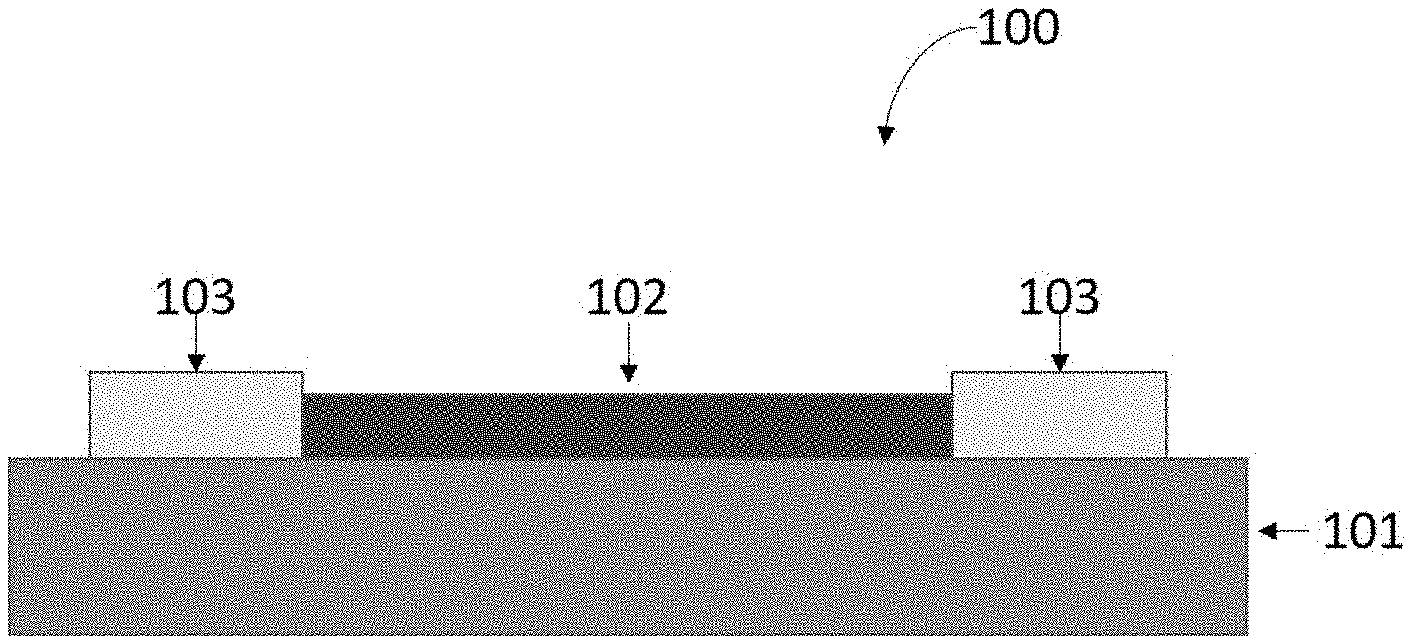
[0011] FIG. 1 shows a cross-sectional view of a PCM resistive memory 100 in accordance with at least one example. The PCM resistive memory 100 may include a substrate 101, a PCM layer 102 and electrical contacts 103. The substrate 101 can be formed from a dielectric material such as glass, high resistivity silicon, silicon carbide, sapphire, high temperature plastic foils, etc. The resistive layer 102 may be formed from a Ge--Te layer. The electrical contacts 103 may be formed by Ti/Au, Al, Mo, ITO, AZO, or any other metallization schema which may be employed for the realization of electrical contacts of PCM memristors. The device may have a planar structure, with the PCM layer 102 and the electrical contacts 103 situated in the same plane, on the surface of the substrate element 101.
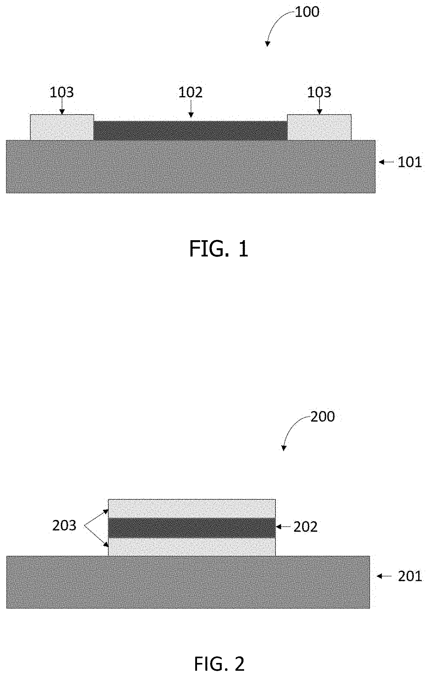
[0012] FIG. 2 shows a cross-sectional view of a PCM resistive memory 100 in accordance with at least one example. The PCM resistive memory 100 may include a substrate 201, a PCM layer 202 and electrical contacts 203. The substrate 201 may be formed from a dielectric material such as glass, high resistivity silicon, silicon carbide, sapphire, high temperature plastic foils, etc. The resistive layer 202 may be formed from a Ge--Te layer. The electrical contacts 203 can be formed by Ti/Au, Al, Mo, ITO, AZO, or any other metallization schema which may be employed for the realization of electrical contacts of PCM memristors. The device may have a vertical structure, with the two contacts 203 placed below and above the PCM layer 202.
[0013] For the fabrication of the resistive memory structures presented in FIG. 1 and FIG. 2, standard procedures employed for PCM memristors may be employed. The PCM layer may be deposited by magnetron sputtering. The electrical contacts may be realized by magnetron sputtering, electron-gun evaporation, thermal evaporation or any other deposition method that are usually used in the field. For defining the resistor and the electrical contacts pattern, standard photolithography, electron-beam lithography, mechanical shadow masks or other techniques that are usually used in the field may be employed.
[0014] The Ge--Te layer may be deposited by magnetron sputtering in an amorphous, high resistive state. The Ge--Te layer may be subjected to a specific thermal treatment which may initiate its transition toward the crystalline state. The degree of the initiated crystallinity depends on the thermal treatment temperature and influence also the electrical resistivity of the Ge--Te layer. This crystalline state initialization process may enable subsequent obtaining of a large number of intermediate resistive states between the initial high resistive state and a final low resistive state. The optimum temperature of the thermal treatment may be between 190-210 C. By employing this treatment, the electrical resistivity of the layer may change from larger than 1*10.sup.4.OMEGA.*cm, for the as deposited layer, to 6*10.sup.-3.OMEGA.*cm.
[0015] After performing this crystalline state initialization process by subjecting the Ge--Te layer to a thermal treatment in inert atmosphere (Ar) at the optimum temperature, the subsequent obtaining of a large number of intermediate resistive states between the high resistive state and a low resistive state may be realized by different methods. For example in one embodiment, the obtaining of a large number of intermediate resistive states may be realized by applying pulses (e.g., voltage pulses, current pulses, etc.) with different amplitudes.
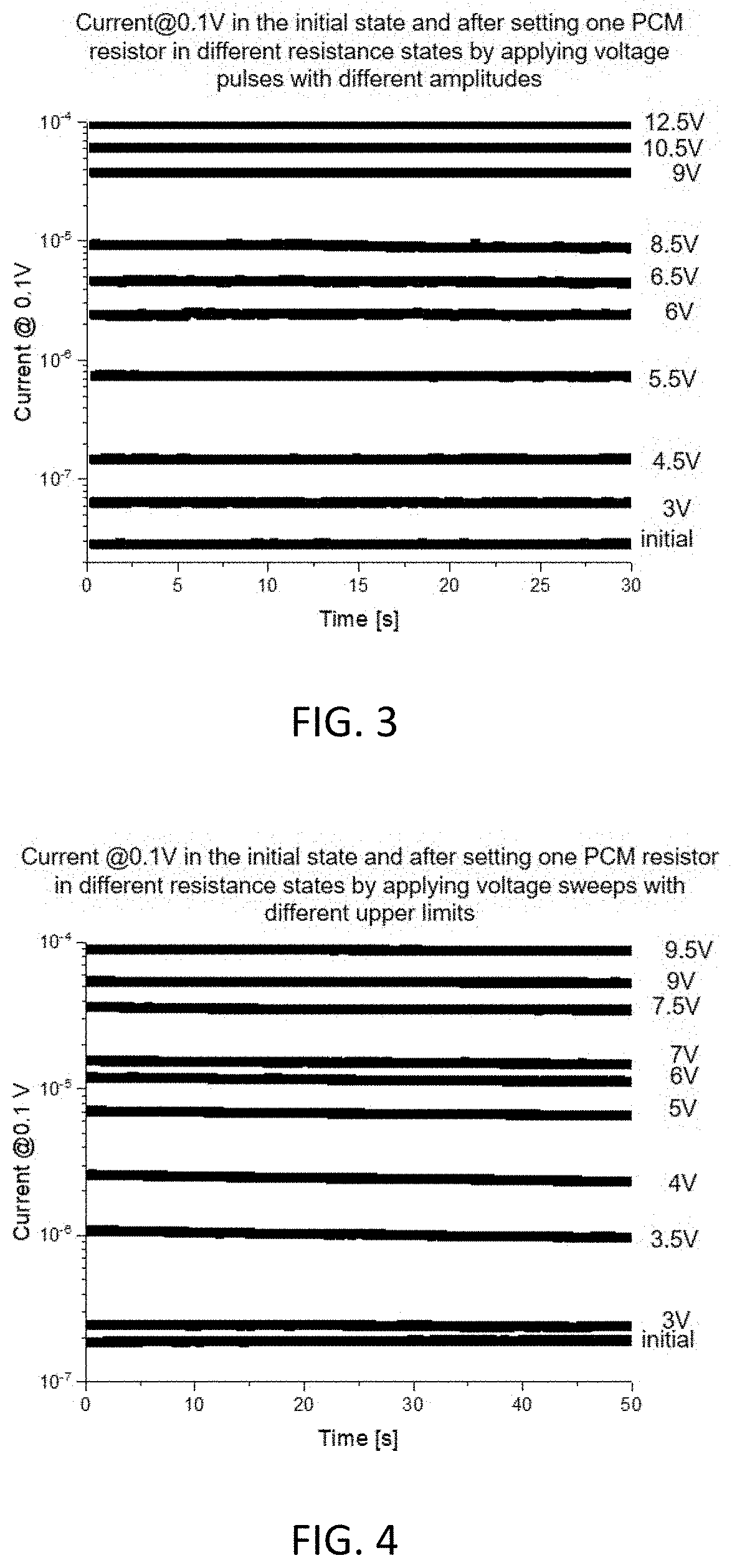
[0016] FIG. 3 shows an example of reading a multiple states PCM planar memory element by measuring the currents flowing through the PCM resistor biased at 0.1V in the initial state and after setting the resistor in different resistance states by applying voltage pulses with different amplitudes.
[0017] As shown in FIG. 3, a large number of various resistance states may be obtained.
[0018] In an embodiment, the obtaining of a large number of intermediate resistive states between the high resistive state and a low resistive state on a previously thermally treated PCM resistor may be realized by performing sweeps (e.g., voltage sweeps) with different upper limits.
[0019] FIG. 4 shows an example of reading a multiple states PCM planar memory element by measuring the currents flowing through the PCM resistor biased at 0.1V in the initial state and after setting the resistor in different resistance states by performing sweeps (e.g., voltage sweeps) with different upper limits.
[0020] As shown in FIG. 4, a large number of various resistance states may be obtained by applying this method.
[0021] In one example, the memory elements described in FIG. 3 and FIG. 4 may be employed as a write once, read many times device. Alternatively, the memory element may change resistive state to increase resistance by applying a short but higher amplitude pulse which may lead to local melting toward more of an amorphous state.
* * * * *
D00000
D00001
D00002
XML
uspto.report is an independent third-party trademark research tool that is not affiliated, endorsed, or sponsored by the United States Patent and Trademark Office (USPTO) or any other governmental organization. The information provided by uspto.report is based on publicly available data at the time of writing and is intended for informational purposes only.
While we strive to provide accurate and up-to-date information, we do not guarantee the accuracy, completeness, reliability, or suitability of the information displayed on this site. The use of this site is at your own risk. Any reliance you place on such information is therefore strictly at your own risk.
All official trademark data, including owner information, should be verified by visiting the official USPTO website at www.uspto.gov. This site is not intended to replace professional legal advice and should not be used as a substitute for consulting with a legal professional who is knowledgeable about trademark law.