Method For Etching A Carbon-containing Feature
Utsuno; Mitsuya ; et al.
U.S. patent application number 16/161744 was filed with the patent office on 2020-04-16 for method for etching a carbon-containing feature. The applicant listed for this patent is ASM IP Holding B.V.. Invention is credited to Dai Ishikawa, Tomohiro Kubota, Mitsuya Utsuno.
| Application Number | 20200118811 16/161744 |
| Document ID | / |
| Family ID | 70160661 |
| Filed Date | 2020-04-16 |


| United States Patent Application | 20200118811 |
| Kind Code | A1 |
| Utsuno; Mitsuya ; et al. | April 16, 2020 |
METHOD FOR ETCHING A CARBON-CONTAINING FEATURE
Abstract
Methods for etching a carbon-containing feature are provided. The methods may include: providing a substrate having a carbon-containing feature formed thereon in a reaction space; supplying helium gas and an oxidizing to the reaction space; generating a plasma within the reaction space from a gas mixture comprising helium gas and the oxidizing gas; and anisotropically etching the carbon-containing feature utilizing the plasma to cause lateral etching of the carbon-containing feature.
| Inventors: | Utsuno; Mitsuya; (Tokyo, JP) ; Kubota; Tomohiro; (Tokyo, JP) ; Ishikawa; Dai; (Tokyo, JP) | ||||||||||
| Applicant: |
|
||||||||||
|---|---|---|---|---|---|---|---|---|---|---|---|
| Family ID: | 70160661 | ||||||||||
| Appl. No.: | 16/161744 | ||||||||||
| Filed: | October 16, 2018 |
| Current U.S. Class: | 1/1 |
| Current CPC Class: | H01L 21/0273 20130101; H01L 21/31138 20130101; H01L 21/31127 20130101; H01J 37/32009 20130101 |
| International Class: | H01L 21/027 20060101 H01L021/027; H01L 21/311 20060101 H01L021/311 |
Claims
1. A method for etching a carbon-containing feature, the method comprising: providing a substrate having a carbon-containing feature formed thereon in a reaction space; supplying helium gas and an oxidizing gas to the reaction space; generating a plasma from a gas mixture comprising helium gas and the oxidizing gas; and anisotropically etching the carbon-containing feature utilizing the plasma to cause lateral etching of the carbon-containing feature,. wherein the substrate is disposed between electrodes in the reaction space and generating a plasma from the gas mixture further comprises applying an RF power of less than 50 W between the electrodes.
2. The method of claim 1, wherein the carbon-containing feature comprises at least one of a photoresist, a chemical amplified resist (CAR), an extreme ultra violet (EUV) resist, or an amorphous carbon.
3. The method of claim 1, wherein the lateral etching of the carbon-containing feature reduces a line edge roughness (LER) of the carbon-containing feature.
4. The method of claim 1, wherein the RF power is less than 15.
5. The method of claim 1, wherein anisotropically etching the carbon-containing feature utilizing the plasma further comprises a ratio of the lateral etch (.DELTA.W) to the height etch (.DELTA.H) of the carbon-containing feature of at least 1:1.2.
6. The method of claim 1, wherein the oxidizing gas comprising at least one of ozone (O.sub.3), nitrogen monoxide (NO), nitrous oxide (N.sub.2O), nitrogen dioxide (NO.sub.2), or carbon dioxide (CO.sub.2).
7. The method of claim 6, wherein the oxidizing gas comprises at least one of ozone (O.sub.3), nitrogen dioxide (NO.sub.2), or carbon dioxide (CO.sub.2).
8. The method of claim 1, wherein the gas mixture within the reaction space comprises a volume ratio of the helium gas to the oxidizing gas in a range from approximately 0.5:1 to approximately 20:1.
9. The method of claim 1, further comprising etching a portion of the substrate utilizing the etched carbon-containing feature as an etch mask.
10. The method of claim 1, further comprising modifying an exposed surface of the substrate utilizing the etched carbon-feature to mask select regions of the substrate.
11. The method of claim 1, further comprising depositing a layer of material over the etched carbon-containing feature.
12. The method of claim 11, wherein the layer of material is conformal to the etched carbon-containing feature.
13. The method of claim 11, wherein the layer of material is non-conformal to the etched carbon-containing feature.
14. The method of claim 11, wherein the layer of material comprises a silicon oxide, a silicon nitride, a silicon carbide, a silicon oxycarbide, a titanium oxide, or a titanium nitride.
15. The method of claim 1, wherein the substrate is disposed between a top electrode and a bottom electrode, wherein the semiconductor is placed on the bottom electrode, wherein the top electrode is disposed above the semiconductor in the reaction space, and wherein the temperature of the bottom electrode is less than 200.degree. C.
16. The method of claim 1, wherein generating the plasma comprises generating the plasma remotely from the reaction space.
17. The method of claim 1, wherein generating the plasma comprises generating the plasma within the reaction space.
18. A method for etching a carbon-containing feature, the method comprising: providing a substrate having a carbon-containing feature formed thereon in a reaction space; supplying helium gas and an oxidizing gas to the reaction space; generating a plasma within the reaction space from a gas mixture comprising helium gas and the oxidizing gas and anisotropically etching the carbon-containing feature utilizing the plasma to cause lateral etching of the carbon-containing feature,. wherein the carbon-containing feature comprises at least one of a chemical amplified resist (CAR), an extreme ultraviolet (EUV) resist, or an amorphous carbon material.
19. A method for etching a carbon-containing feature, the method comprising: providing a substrate having a carbon-containing feature formed thereon in a reaction space; supplying helium gas and an oxidizing gas to the reaction space; generating a plasma within the reaction space from a gas mixture comprising helium gas and the oxidizing gas and anisotropically etching the carbon-containing feature utilizing the plasma to cause lateral etching of the carbon-containing feature, wherein the pressure within the reaction space is controlled at less than 800 Pascals.
Description
FIELD OF INVENTION
[0001] The present disclosure generally relates to methods for etching a carbon-containing feature and particularly methods for anisotropically etching a carbon-containing feature to thereby reduce the lateral width of the carbon-containing feature.
BACKGROUND OF THE DISCLOSURE
[0002] The down scaling of semiconductor device structures, such as, for example, complementary metal-oxide-semiconductor (CMOS) devices, has led to significant improvements in speed and density of integrated circuits. However, conventional device scaling faces immense challenges for future technology nodes.
[0003] Reducing the dimensions and spacing of semiconductor device features places ever increasing demands on the method used to form the features. For example, due to limitations imposed by optics and radiation wavelengths, many conventional photolithographic methods cannot facilitate the formation of features having critical dimensions less than approximately 40 nanometers. Electron beam (E-Beam) lithography and extreme ultraviolet (EUV) lithography have been used to form features having critical dimensions below 40 nanometers, but generally require complex processes and significant costs.
[0004] The patterning and etching of semiconductor device structures may be achieved utilizing a carbon-containing material, such as, for example, a chemical photoresist. For example, the process of etching a pattern into a semiconductor device structure may comprise the use of a mask to selectively allow an etchant to remove the useful layers of the semiconductor device structure, as required to form the desired pattern. Typically, a mask is formed by spin coating a layer of liquid photoresist on the materials to be etched. The desired pattern on the photoresist is then exposed to a form of radiation, for example, through use of an optical mask and ultraviolet light. The exposed areas of the photoresist are rendered either soluble or insoluble to a corresponding chemical developer, depending on whether the photoresist is a positive type resist or a negative type resist. The soluble portions of the photoresist are then removed, and the remaining photoresist functions as a mask for selectively allowing an etchant to remove underlying material in areas void of photoresist protection.
[0005] A problem may arise when the critical dimension (CD) of the patterned formed from the carbon-containing material, e.g., a photoresist feature, is larger than the feature size required on the semiconductor device structure. One method of reducing the critical dimension of a feature comprising a carbon-containing material, such as, for example, a photoresist line, is to expose the feature to etching conditions, also commonly referred to as "trimming." For example, a trimming process may be utilized to reduce a critical dimension of a carbon-containing feature, e.g., the lateral width of a photoresist line. Trimming processes commonly employ the formation of an ionized plasma to remove portions of the carbon-containing features, thereby reducing the lateral width of the feature, i.e., a reduction in the line width of a line of photoresist. However, the ionized plasma utilized to etch the carbon-containing resist feature generally comprises ions that are vertically irradiated to the substrate upon which the carbon-containing features are disposed, which may result in a preferential reduction in the height of the carbon-containing resist features as opposed to a preferred reduction in the lateral width. Accordingly, methods are desirable that are able to simply enhance the rate of lateral etch compared with the rate of height etch of a carbon-containing resist feature to enable a reduction in the critical dimension of the carbon-containing feature whilst maintaining a substantial height of the carbon-containing feature for subsequent processes.
SUMMARY OF THE DISCLOSURE
[0006] In accordance with at least one embodiment of the disclosure, a method for etching a carbon-containing feature is disclosed. The method may comprise: providing a substrate having a carbon-containing features formed thereon in a reaction space; supplying helium gas and an oxidizing gas to the reaction space; generating a plasma within the reaction space from a gas mixture comprising helium gas and the oxidizing gas; and anisotropically etching the carbon-containing feature utilizing the plasma to cause lateral etching of the carbon-based feature.
[0007] For the purpose of summarizing the invention and the advantages achieved over the prior art, certain objects and advantages of the invention have been described herein above. Of course, it is to be understood that not necessarily all such objects or advantages may be achieved in accordance with any particular embodiment of the invention. Thus, for example, those skilled in the art will recognize that the invention may be embodied or carried out in a manner that achieves or optimizes one advantage or group of advantages as taught or suggested herein without necessarily achieving other objects or advantages as may be taught or suggested herein.
[0008] All of these embodiments are intended to be within the scope of the invention herein disclosed. These and other embodiments will become readily apparent to those skilled in the art from the following detailed description of certain embodiments having reference to the attached figures, the invention not being limited to any particular embodiment(s) disclosed.
BRIEF DESCRIPTION OF THE DRAWING FIGURES
[0009] While the specification concludes with claims particularly pointing out and distinctly claiming what are regarded as embodiments of the invention, the advantages of embodiments of the disclosure may be more readily ascertained from the description of certain examples of the embodiments of the disclosure when read in conjunction with the accompanying drawing, in which:
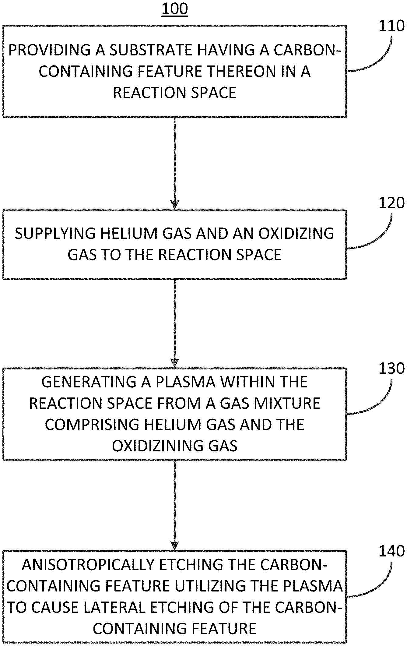
[0010] FIG. 1 illustrates a process flow diagram illustrating an exemplary method in accordance with the embodiments of the disclosure;
[0011] FIGS. 2A and 2B illustrate cross sectional schematic diagrams of semiconductor structures formed during an exemplary process flow in accordance with the embodiments of the disclosure;
[0012] FIG. 3 illustrates optical emission spectra (OES) from a number of exemplary plasmas in accordance with the embodiments of the disclosure;
[0013] FIGS. 4A and 4B illustrate scanning transmission electron microscope (STEM) images of semiconductor structures formed in accordance with the embodiments of the disclosure; and
[0014] FIGS. 5A-5D illustrate cross sectional schematic diagrams of applications for the etched carbon-containing feature in accordance with the embodiments of the disclosure.
[0015] It will be appreciated that elements in the figures are illustrated for simplicity and clarity and have not necessarily been drawn to scale. For example, the dimensions of some of the elements in the figures may be exaggerated relative to other elements to help improve understanding of illustrated embodiments of the present disclosure.
DETAILED DESCRIPTION OF EXEMPLARY EMBODIMENTS
[0016] Although certain embodiments and examples are disclosed below, it will be understood by those in the art that the invention extends beyond the specifically disclosed embodiments and/or uses of the invention and obvious modifications and equivalents thereof. Thus, it is intended that the scope of the invention disclosed should not be limited by the particular disclosed embodiments described below.
[0017] As used herein, the term "substrate" may refer to any underlying material or materials that may be used, or upon which, a device, a circuit or a film may be formed.
[0018] In the specification, it will be understood that the term "on" or "over" may be used to describe a relative location relationship. Another element or layer may be directly on the mentioned layer, or another layer (an intermediate layer) or element may be intervened therebetween, or a layer may be disposed on a mentioned layer but not completely cover a surface of the mentioned layer. Therefore, unless the term "directly" is separately used, the term "on" or "over" will be construed to be a relative concept. Similarly to this, it will be understood the term "under," "underlying," or "below" will be construed to be relative concepts.
[0019] The embodiments of the disclosure may include methods for etching a carbon-containing feature disposed upon a substrate and particularly methods for reducing the lateral width, i.e., the critical dimension, of a carbon-containing resist feature utilizing a plasma within a reaction space, wherein the plasma is created from a gas mixture comprising at least helium gas and an oxidizing gas.
[0020] Methods are known for improving the etch ratio of the lateral width of a carbon-containing resist feature compared with the height of the carbon-containing resist feature and generally comprise methods for hardening the upper exposed surface of the carbon-containing resist feature. For example, hardening the upper exposed surface of the carbon-containing resist feature may decrease the ability of the vertically impinging ions from the plasma from reducing the height of the carbon-containing features. Methods utilized to harden the upper exposed surface of the carbon-containing resist feature may comprise irradiating the surface of the resist feature with high energy particles, such as, for example, by irradiating with either an electron beam or a ion beam. However, such methods of irradiating the carbon-containing feature to reduce the etch rate in the vertical direction of the resist feature, i.e., a reduction in the etch rate of the height of the resist feature, involves the addition of a further complex process step and accordingly methods are desirable for "trimming" a carbon-containing feature without the need for additional processes, such as, for example, high energy irradiation processes.
[0021] The embodiments of the disclosure may therefore include methods for etching a carbon-containing feature, the methods comprising: providing a substrate having a carbon-containing feature formed thereon in a reaction space; supplying helium gas and an oxidizing gas to the reaction space; generating a plasma within the reaction space from a gas mixture comprising helium gas and the oxidizing gas; and anisotropically etching the carbon-containing feature utilizing the plasma to cause lateral etching of the carbon-containing feature.
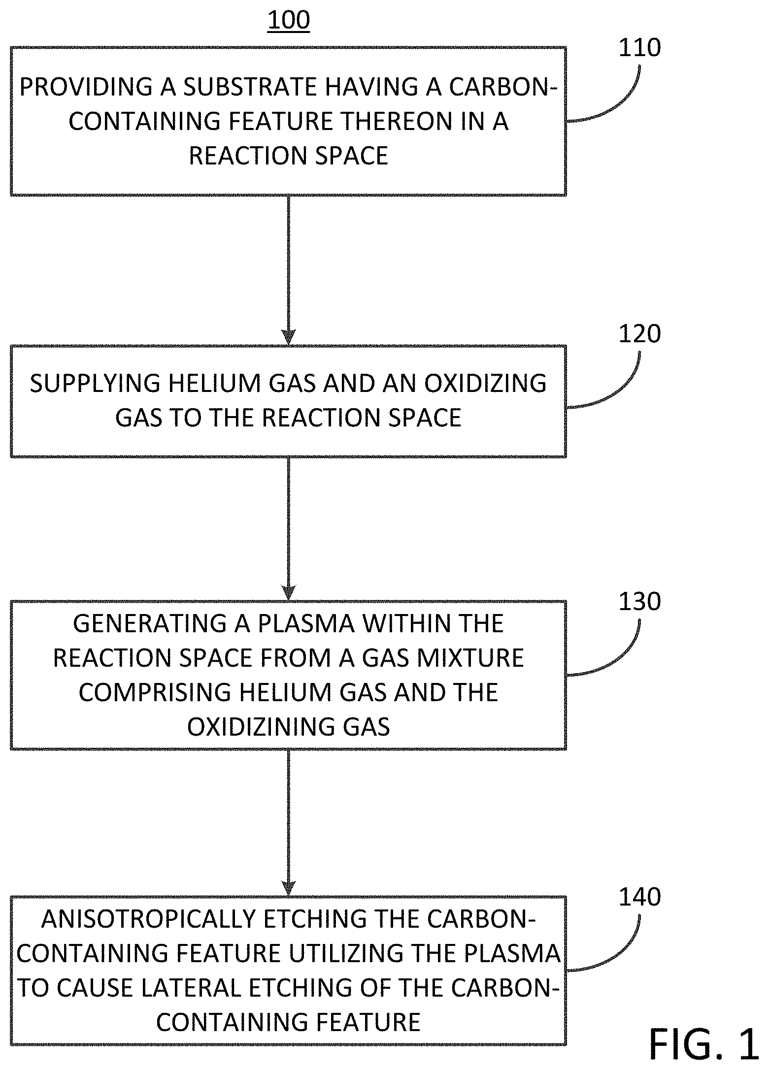
[0022] The methods of the disclosure are described in greater detail with reference to FIG. 1 which comprises a process flow diagram illustrating an exemplary method 100 and with reference to FIGS. 2A and 2B which illustrate cross sectional schematic diagrams of semiconductor structures formed as part of the process flow of exemplary method 100.
[0023] The method 100 may commence with a process block 110 comprising, providing a substrate having a carbon-containing feature disposed thereon in a reaction space. In greater detail, the process may comprise providing a substrate, such as substrate 202 of semiconductor structure 200 (FIG. 2A). In some embodiments of the disclosure, the substrate 202 may comprise a planar substrate (as illustrated in FIG. 2A) or a patterned substrate. The substrate 202 may comprise one or more materials including, but not limited to, silicon (Si), germanium (Ge), germanium tin (GeSn), silicon germanium (SiGe), silicon germanium tin (SiGeSn), silicon carbide (SiC), or a group III-V semiconductor material, such as, for example, gallium arsenide (GaAs), gallium phosphide (GaP), or gallium nitride (GaN). In some embodiments of the disclosure, the substrate 202 may comprise an engineered substrate wherein a surface semiconductor layer is disposed over a bulk support with an intervening buried oxide (BOX) disposed there between.
[0024] Patterned substrates may comprise substrates that may include semiconductor device structures formed into or onto a surface of the substrate, for example, a patterned substrate may comprise partially fabricated semiconductor device structures, such as, for example, transistors and/or memory elements. In some embodiments, the substrate may contain monocrystalline surfaces and/or one or more secondary surfaces that may comprise a non-monocrystalline surface, such as a polycrystalline surface and/or an amorphous surface. Monocrystalline surfaces may comprise, for example, one or more of silicon (Si), silicon germanium (SiGe), germanium tin (GeSn), or germanium (Ge). Polycrystalline or amorphous surfaces may include dielectric materials, such as oxides, oxynitrides or nitrides, such as, for example, silicon oxides and silicon nitrides.
[0025] In some embodiments of the disclosure, the substrate 202 has a carbon-containing feature 204 disposed thereon, for example, the carbon-containing feature may be disposed on, or directly on, the upper surface of the substrate 202. In some embodiments, the carbon-containing feature 204 may comprise a chemical photoresist which may be ultimately utilized as a patterned masking material. In some embodiments of the disclosure, the carbon-containing feature 204 may comprise at least one of a photoresist, a chemical amplified resist (CAR), an extreme ultraviolet (EUV) resist, or an amorphous carbon material. In some embodiments, the carbon-containing feature 204 may be formed by standard photolithographic/electron beam and development processes which are well known in the art and are therefore not described herein. In some embodiments, the carbon-containing feature may comprise a line feature, open pore feature, a gap feature, a circular feature, or any geometry, dimension and configuration of a carbon-containing resist material that may be formed depending on the exposure and the associated development process.
[0026] In some embodiments, the carbon-containing feature 204 may comprise a photoresist line feature (as illustrated in cross section in FIG. 2A), wherein the photoresist line may have a pre-etch height (H.sub.1), a pre-etch lateral width (W.sub.1), and pre-etch aspect ratio (H.sub.1:W.sub.1).
[0027] One parameter that may be utilized to determine the quality of a carbon-containing feature, such as a photoresist line, is the line edge roughness (LER) which may comprise the variation in the width of a resist line feature that occurs along the length of the feature, for example, an examination of the variation in the width of the carbon-containing feature along one edge of the feature may be referred to as the LER. LER may become an important parameter as feature sizes decrease on the order of 100 nanometers or less and may become a significant source of linewidth control problems for features below approximately 50 nanometers. LER may be characterized as the 3-sigma deviation of a line edge from a straight line and commonly becomes more of a significant problem as the critical dimension of the carbon-containing feature decreases in size.
[0028] In some embodiments of the disclosure, the semiconductor structure 200 comprising the substrate 202 with the carbon-containing feature 204 disposed thereon is provided in a reaction space of a semiconductor processing apparatus, such as, for example, a semiconductor processing apparatus configured for supplying a plasma to the surface of the semiconductor structure 200. In some embodiments, the semiconductor processing apparatus may comprise a plasma etching apparatus, such as, for example, a reactive ion etcher (ME), inductively coupled plasma (ICP) etcher, or an electron cyclotron resonance (ECR) etcher. In some embodiments, the semiconductor processing apparatus may comprise a plasma based deposition system, such as, for example, a plasma-enhanced chemical vapor deposition (PECVD) system, or an plasma-enhanced atomic layer deposition (PEALD) system.
[0029] In some embodiments of the disclosure, the semiconductor structure 200 may be disposed within the reaction space between electrodes configured for generating a plasma within the reaction space, e.g., the semiconductor structure 200 may be placed on a bottom electrode and a top electrode may disposed above the semiconductor structure 200. In some embodiments of the disclosure, the bottom electrode may comprise one or more temperature control elements, wherein the temperature of the bottom electrode may be raised or lowered depending on the desired process parameters. For example, the temperature of the bottom electrode may be at less than approximately 200.degree. C., or less than approximately 100.degree. C., or even less than approximately 25.degree. C. In some embodiments, the temperature of the bottom electrode may be between approximately 25.degree. C. and approximately 200.degree. C.
[0030] In some embodiments of the disclosure, the generation of the plasma may take place remotely from the reaction space and subsequently the plasma may be introduced into the reaction space to interact with the carbon-containing feature 204 disposed upon the substrate 202.
[0031] The exemplary method 100 (FIG. 1) may continue with a process block 120 which comprises, supplying helium gas and an oxidizing gas into the reaction space. In some embodiments of the disclosure, the oxidizing gas may comprise at least one of molecular oxygen (O.sub.2), ozone (O.sub.3), nitrogen monoxide (NO), nitrous oxide (N.sub.2O), nitrogen dioxide (NO.sub.2), or carbon dioxide (CO.sub.2). In some particular embodiments, the oxidizing gas may comprise molecular oxygen (O.sub.2). In some embodiment, the flow rate ratio of helium flow to oxidizing gas flow (helium flow:oxidizing gas glow) may be in range from approximately 0.5:1 to approximately 20:1.
[0032] Supplying helium gas and an oxidizing gas to the reaction space may form a gas mixture within the reaction space comprising at least helium gas and the oxidizing gas. In some embodiments of the disclosure, the gas mixture within the reaction space comprises a volume ratio of helium gas to oxidizing gas in a range from approximately 0.5:1 to approximately 20:1.
[0033] In addition to controlling the temperature of the substrate and the flow of helium and oxidizing gas in the reaction space, the embodiments of the disclosure may also control the pressure within the reaction space. For example, the pressure within the reaction space may be controlled at less than 800 Pascals, or less than 600 Pascals, or less than 400 Pascals, or less than 200 Pascals, or even less than 150 Pascals. In some embodiments of the disclosure, the pressure within the reaction space may be controlled between approximately 150 Pascals and approximately 800 Pascals.
[0034] The exemplary method 100 (FIG. 1) may continue with a process block 130 comprising, generating a plasma within the reaction space from a gas mixture comprising helium gas and an oxidizing gas. In some embodiments, the semiconductor structure 200 (FIG. 2A) may be disposed in a reaction space of a semiconductor processing apparatus configured for supplying a plasma to the surface of the semiconductor structure 200. As a non-limiting example, in some embodiments, the semiconductor structure 200 may disposed between electrodes in the reaction space and generating a plasma from the gas mixture may further comprise applying an RF power of less than 100 Watts, or less than 50 Watts, or less than 30 Watts, or less than 20 Watts, or even less than 15 Watts, between the electrodes. In some embodiments of the disclosure, the RF power supplied between the electrodes may be between approximately 15 Watts and approximately 100 Watts.
[0035] In some embodiments, generating a plasma from the gas mixture comprising helium and an oxidizing gas may further comprise the generation of oxygen radicals which may be utilized to anisotropically etch a carbon-containing feature disposed in the reaction space. Not to be bound by any particular theory, but it is believed that utilizing a gas mixture comprising both helium gas and an oxidizing gas may increase the generation of oxygen radicals in the plasma and thereby enhance the lateral etch rate of a carbon-containing feature.
[0036] As a non-limiting example, FIG. 3 illustrates the optical emission spectra (OES) from a number of example plasmas, wherein the data represented by line 300 is taken from a plasma generated from a gas mixture comprising helium and molecule oxygen (O.sub.2), the data represented by line 302 is taken from a plasma generated from a gas mixture comprising argon and molecule oxygen (O.sub.2), and the data represented by line 304 is taken from a plasma generated from molecular oxygen (O.sub.2).
[0037] The density of oxygen radicals in the example plasmas may be determined by examination of the peak intensity at 777 nanometers of the OES spectrum of FIG. 3.
[0038] Examination of the 777 nanometer peak in the OES of FIG. 3 clearly indicates that the intensity of the spectra is significantly higher for the plasma generated from the gas mixture comprising helium and molecular oxygen (O.sub.2) (data labelled 300) and therefore the density of oxygen radicals is greatest in the plasma comprising both helium and molecular oxygen (O.sub.2).
[0039] The exemplary method 100 (FIG. 1) may continue with a process block 140 which comprises, anisotropically etching the carbon-containing feature utilizing the plasma to cause lateral etching of the carbon-containing feature. In more detail, FIG. 2B illustrates a semiconductor structure 206 which comprising an exemplary etched carbon-containing feature 204' after being exposed to the plasma generated from a gas mixture comprising both helium gas and an oxidizing gas. As illustrated in FIG. 2B, the exemplary carbon-containing feature 204' has a reduced height of H.sub.2 and a reduced lateral width of W.sub.2, when compared with the pre-etch carbon-containing features which has a height H.sub.1 and a lateral width W.sub.1. For example, the reduction in the height of the carbon-containing feature 204' can be expressed as .DELTA.H (i.e., H.sub.1-H.sub.2) and the reduction in the lateral width of the carbon-containing feature 204' can be expressed as .DELTA.W (i.e., W.sub.1-W.sub.2). In some embodiments of the disclosure, anisotropically etching the carbon-containing feature utilizing the plasma may further comprise a ratio of the lateral etch (.DELTA.W) to height etch (.DELTA.H) (i.e., .DELTA.W:.DELTA.H) of at least 1:1.2.
[0040] In some embodiments of the disclosure, laterally etching the carbon containing feature may further comprise reducing the line edge roughness (LER) of the carbon-containing feature.
[0041] As a non-limiting example, FIGS. 4A and 4B illustrate cross sectional scanning transmission electron microscope (STEM) images of extreme ultraviolet (EUV) resist patterns pre-etch (FIG. 4A) and post-etch (FIG. 4B) at the same magnification level. In more detail,
[0042] FIG. 4A illustrates a STEM image of EUV resist pattern 400 on a substrate 402 prior to being etched, it should be noted that the dark region observed around the EUV resist 400 is due to a thin film of platinum utilized in the STEM imaging process. In the non-limiting example embodiment the substrate 402 with the EUV resist 400 disposed thereon was introduced into the reaction space of a plasma-enhanced atomic layer deposition (PEALD) apparatus and a mixture of helium gas and molecular oxygen (O.sub.2) was introduced into the reaction space at a flow rate ratio of 1:1, the flow rate monitored by mass flow controllers. A plasma was generated in the reaction space from the gas mixture comprising both helium and molecular oxygen. The RF power for generating the plasma was 15 Watts and the exposure time of the EUV resist pattern 400 to the plasma was approximately 10 seconds. FIG. 4B illustrates a STEM image of the EUV resist pattern 400' on the substrate 402 post-etch, wherein the lateral width of the EUV resist pattern 400' has reduced (.DELTA.W) by an amount of 2.75 nanometers and the height of the EUV resist pattern 400' has reduced (.DELTA.H) by an amount of 3.30 nanometers, resulting a .DELTA.W:.DELTA.H ratio of 1:1.2.
[0043] The etched, or "trimmed," carbon-containing feature, such as a photoresist line with reduced lateral width, may be utilized in a number of applications. For example, in some embodiments, the methods of the disclosure may further comprise etching a portion of the substrate utilizing the etched carbon-containing feature as an etch mask. In more detail and with reference to FIG. 5A, a semiconductor structure 500 may include the etched carbon-containing feature 204', such as, for example, a photoresist line pattern with a reduced lateral width which may be utilized as an etch mask to fabricate patterns in the underlying substrate 502, the pattern etched into the substrate having a critical dimension less than that achievable without the etched carbon-containing feature 204'. As illustrated in FIG. 5A, the etched carbon-containing feature 204' masks, i.e., cover or protects, a select portion of the underlying substrate 502 such that the exposed regions of the substrate, i.e., those areas without an overlying carbon-containing feature, may be exposed to one or more etchants, such as, for example, a wet etchant or a plasma etchant, resulting in etched substrate 502.
[0044] In further example embodiments, the etched carbon-containing feature may be utilized as a mask to protect select regions of the surface of a substrate from a surface modifying species. For example, and with reference to FIG. 5B, a semiconductor structure 504 may include the etched carbon-containing feature 204', such as, for example, a photoresist line with reduced lateral width, which may be disposed over a substrate 506 and selectively masks, i.e., covers or protects, select regions of the substrate from a surface modifying species. The portions of the substrate 506 which are not covered by the etched carbon-containing feature 204', i.e., the exposed surface 508 of substrate 506, may be treated by one or more surface modifying species to thereby alter the surface properties of the exposed surface 508. For example, the exposed surface 508 may be treated with oxygen precursor to oxidize select portions of the surface of the substrate 506.
[0045] In yet further example embodiments, the methods disclosed herein may further comprise depositing a layer of material over the etched carbon-containing feature. As non-limiting examples, a layer of material may be deposited over the etched carbon-containing feature 204' utilizing either conformal deposition methods to form a conformal film over the etched carbon-containing feature, as illustrated by the semiconductor structure 510 including the conformal film 512 disposed over substrate 514 (FIG. 5C), or a layer of material may be deposited over the etched carbon-containing feature 204' utilizing non-conformal deposition methods to form semiconductor structure 516 including non-conformal film 518 disposed over substrate 520 (FIG. 5D). In some embodiments of the disclosure, the layer of material may comprise at least one of a silicon oxide, a silicon nitride, a silicon carbide, a silicon oxycarbide, a titanium oxide, or a titanium nitride.
[0046] The example embodiments of the disclosure described above do not limit the scope of the invention, since these embodiments are merely examples of the embodiments of the invention, which is defined by the appended claims and their legal equivalents. Any equivalent embodiments are intended to be within the scope of this invention. Indeed, various modifications of the disclosure, in addition to those shown and described herein, such as alternative useful combination of the elements described, may become apparent to those skilled in the art from the description. Such modifications and embodiments are also intended to fall within the scope of the appended claims.
* * * * *
D00000
D00001
D00002
D00003
D00004
D00005
D00006
XML
uspto.report is an independent third-party trademark research tool that is not affiliated, endorsed, or sponsored by the United States Patent and Trademark Office (USPTO) or any other governmental organization. The information provided by uspto.report is based on publicly available data at the time of writing and is intended for informational purposes only.
While we strive to provide accurate and up-to-date information, we do not guarantee the accuracy, completeness, reliability, or suitability of the information displayed on this site. The use of this site is at your own risk. Any reliance you place on such information is therefore strictly at your own risk.
All official trademark data, including owner information, should be verified by visiting the official USPTO website at www.uspto.gov. This site is not intended to replace professional legal advice and should not be used as a substitute for consulting with a legal professional who is knowledgeable about trademark law.