High-efficiency Optical Limiter Using Metasurface And Phase-change Material
Valentine; Jason G. ; et al.
U.S. patent application number 16/593551 was filed with the patent office on 2020-04-16 for high-efficiency optical limiter using metasurface and phase-change material. The applicant listed for this patent is Vanderbilt University. Invention is credited to Richard F. Haglund, Austin Howes, Jason G. Valentine, Zhihua Zhu.
| Application Number | 20200117070 16/593551 |
| Document ID | / |
| Family ID | 70161254 |
| Filed Date | 2020-04-16 |


| United States Patent Application | 20200117070 |
| Kind Code | A1 |
| Valentine; Jason G. ; et al. | April 16, 2020 |
HIGH-EFFICIENCY OPTICAL LIMITER USING METASURFACE AND PHASE-CHANGE MATERIAL
Abstract
According to some aspects, a transmissive and all-dielectric optical component/limiter with great cutoff efficiency using Vanadium Dioxide (VO.sub.2) as the active component is disclosed. In some embodiments, Vanadium dioxide is used for an optical limiter due to the large contrast in optical constants upon undergoing the semiconductor to metal phase transition. When triggered optically, this transition occurs within 60 fs, making the device suitable for an ultrafast laser environment. In addition, the phase transition threshold is tunable by applying stress or doping; therefore, the device cutoff intensity can be adjusted to fulfill specific requirements.
| Inventors: | Valentine; Jason G.; (Nashville, TN) ; Haglund; Richard F.; (Nashville, TN) ; Zhu; Zhihua; (Nashville, TN) ; Howes; Austin; (Nashville, TN) | ||||||||||
| Applicant: |
|
||||||||||
|---|---|---|---|---|---|---|---|---|---|---|---|
| Family ID: | 70161254 | ||||||||||
| Appl. No.: | 16/593551 | ||||||||||
| Filed: | October 4, 2019 |
Related U.S. Patent Documents
| Application Number | Filing Date | Patent Number | ||
|---|---|---|---|---|
| 62741917 | Oct 5, 2018 | |||
| Current U.S. Class: | 1/1 |
| Current CPC Class: | G02F 2001/3507 20130101; G02F 1/3523 20130101; G02F 2001/3509 20130101; G02F 1/3556 20130101; G02F 2202/30 20130101; G02F 2203/15 20130101; G02F 2203/52 20130101; G02F 1/3501 20130101; G02F 1/3558 20130101 |
| International Class: | G02F 1/35 20060101 G02F001/35; G02F 1/355 20060101 G02F001/355 |
Goverment Interests
STATEMENT REGARDING GOVERNMENT SUPPORT
[0002] This invention was made with government support under Grant Number N00014-16-1-2283 awarded by Office of Naval Research ("ONR"), under Grant No. ECCS1351334 awarded by National Science Foundation ("NSF"), and under Grant No. DE-FG02-01ER45916 awarded by the Department of Energy. The government has certain rights to this invention.
Claims
1. An optical component, comprising: a dielectric resonator; and a phase-change material on the dielectric resonator, the phase-change material having an optical property having a first characteristic associated with a first material phase and a second characteristic associated with a second material phase.
2. The optical component of claim 1, wherein the dielectric resonator has a cylindrical profile having a height H.sub.res and diameter D.sub.res and wherein phase-change material has a cylindrical profile having a height t.sub.pcm and a diameter D.sub.pcm, wherein D.sub.res=D.sub.pcm and the phase-change material is on the dielectric resonator such that a total height H.sub.tot of the optical component H.sub.tot=H.sub.res+t.sub.pcm.
3. The optical component of claim 1, wherein the dielectric resonator comprises Si and the phase-change material comprises VO.sub.2.
4. The optical component of claim 3, wherein the VO.sub.2 extends from the surface of the Si a predetermined thickness.
5. The optical component of claim 4, wherein the VO.sub.2 has a cylindrical profile having a height t.sub.VO.sub.2 and diameter D.sub.VO.sub.2 and wherein the Si has a cylindrical profile having a height h.sub.Si and a diameter D.sub.Si.
6. The optical component of claim 4, wherein t.sub.VO.sub.2=30 nm and h.sub.Si=180 nm and D.sub.VO.sub.2=D.sub.Si.
7. The optical component of claim 1, wherein the first characteristic is semiconducting and the second characteristic is reflectivity.
8. The optical component of claim 1, wherein an electric dipole of the dielectric resonator and a magnetic dipole of the dielectric resonator are spectrally overlapped at a resonance wavelength.
9. The optical component of claim 1, further comprising an insulating substrate wherein the dielectric resonator is on the substrate and the phase-change material is on the dielectric resonator.
10. An optical device having tunable light transmission properties comprising: an insulating substrate; dielectric resonator structures on the insulating substrate and periodically spaced apart on a surface of the insulating substrate by a predetermined pitch p; and a phase-change material structures, each phase-change material structure corresponding to and located on one of the dielectric resonator structures, wherein each of the phase-change material structures has an optical property having a first characteristic associated with a first material phase and a second characteristic associated with a second material phase.
11. The optical device of claim 10, wherein the pitch p is p.sub.x in a first direction the substrate and p.sub.y in a second direction on the substrate.
12. The optical device of claim 11, wherein p.sub.x=p.sub.y and the first direction is substantially perpendicular to the second direction.
13. The optical device of claim 10, wherein each of the dielectric resonators has a cylindrical profile having a height H.sub.res and diameter D.sub.res and wherein each of the phase-change material structures has a cylindrical profile having a height t.sub.pcm and a diameter D.sub.pcm, wherein D.sub.res=D.sub.pcm and each of the phase-change material structures is on one of the dielectric resonators such that a total height H.sub.tot of an optical component comprising one of the dielectric resonators and one of the phase-change material structures is H.sub.tot=H.sub.res+t.sub.pcm.
14. The optical device of claim 10, wherein the dielectric resonator comprises Si and the phase-change material comprises VO.sub.2.
15. The optical component of claim 14, wherein the VO.sub.2 extends from the surface of the Si a predetermined thickness.
16. The optical device of claim 14, wherein the VO.sub.2 has a cylindrical profile having a height t.sub.VO.sub.2 and diameter D.sub.VO.sub.2 and wherein the Si has a cylindrical profile having a height h.sub.Si and a diameter D.sub.Si.
17. The optical component of claim 16, wherein t.sub.VO.sub.2=30 nm and h.sub.Si=180 nm and D.sub.VO.sub.2=D.sub.Si.
18. The optical device of claim 10, wherein the first characteristic is semiconducting and the second characteristic is reflectivity.
19. The optical device of claim 10, wherein an electric dipole of the dielectric resonator and a magnetic dipole of the dielectric resonator are spectrally overlapped at a resonance wavelength.
Description
CROSS REFERENCE TO RELATED APPLICATIONS
[0001] This application claims priority to and the benefit of U.S. Provisional Patent Application Ser. No. 62/741,917, filed Oct. 5, 2018, the contents of which is hereby incorporated by reference in its entirety.
BACKGROUND
Field of the Endeavor
[0003] Embodiments of the present invention relate to optical devices, specifically tunable optical limiters based on metasurfaces.
Background
[0004] Optical limiters are intended to limit the intensity of light at high fluences. This is typically done to protect electronics or an individual's eyes from exposure to intense and damaging laser light. The demand for efficient power-limiting optical elements has accompanied the development of high-power lasers in order to meet safety requirements and eliminate potential damage on sensitive photodetectors, sensors, and cameras.
[0005] An optical limiter generally transmits low intensity light with a high transmission coefficient (e.g., in an on-state) and blocks high intensity light completely or maintains the transmission coefficient at a sufficiently low level (e.g., in an off-state). In the past few decades, most optical limiter designs have used two-photon absorption or excited state absorption in nonlinear media. These materials have been primarily studied as dilute suspensions and not as complete optical devices, hindering their integration in solid-state platforms for real applications. In addition, nonlinear materials films or suspensions face a tradeoff between the on-state transmission and cut-off contrast, as a thinner material possesses higher on-state transmission but is incapable of blocking light efficiently at the off-state.
[0006] One conventional way for achieving limiting is to use dyes that absorb light. However, these limiters suffer from relative high transmission in the high fluence state. They are also easily damaged by high fluence light. Another approach is to use a cavity with a nonlinear material inside it, but this approach can result in very strong limiting but suffers from a reflection band around the limiting wavelength. As such, this approach is only suitable for protecting cameras or sensors that have a very narrow wavelength range with which they operate across.
BRIEF SUMMARY
[0007] In accordance with the purpose(s) of this invention, as embodied and broadly described herein, this invention, in one aspect, relates to an optical limiter using metasurface and phase-change material.
[0008] It is to be understood that both the foregoing general description and the following detailed description are exemplary and explanatory only and are not restrictive of the invention as claimed.
BRIEF DESCRIPTION OF THE DRAWINGS
[0009] The accompanying figures, which are incorporated herein and form part of the specification, illustrate an optical device using metasurface and phase-change material. Together with the description, the figures further serve to explain the principles of the actively reconfigurable, hyperbolic metasurfaces described herein and thereby enable a person skilled in the pertinent art to make and use the optical device using metasurface and phase-change material.
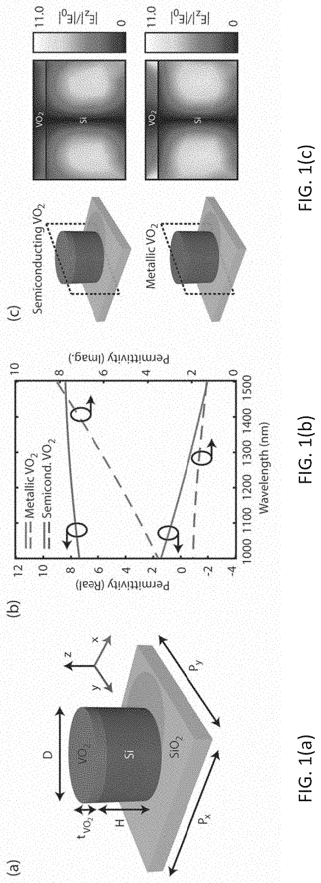
[0010] FIG. 1(a) shows a schematic of an exemplary Huygens metasurface-based optical limiter according to principles described herein.
[0011] FIG. 1(b) shows measured permittivity of a 30 nm Vanadium Dioxide (VO.sub.2) film on Si substrate at 25.degree. C. and 85.degree. C.
[0012] FIG. 1(c) shows an electric field distribution in the z direction.
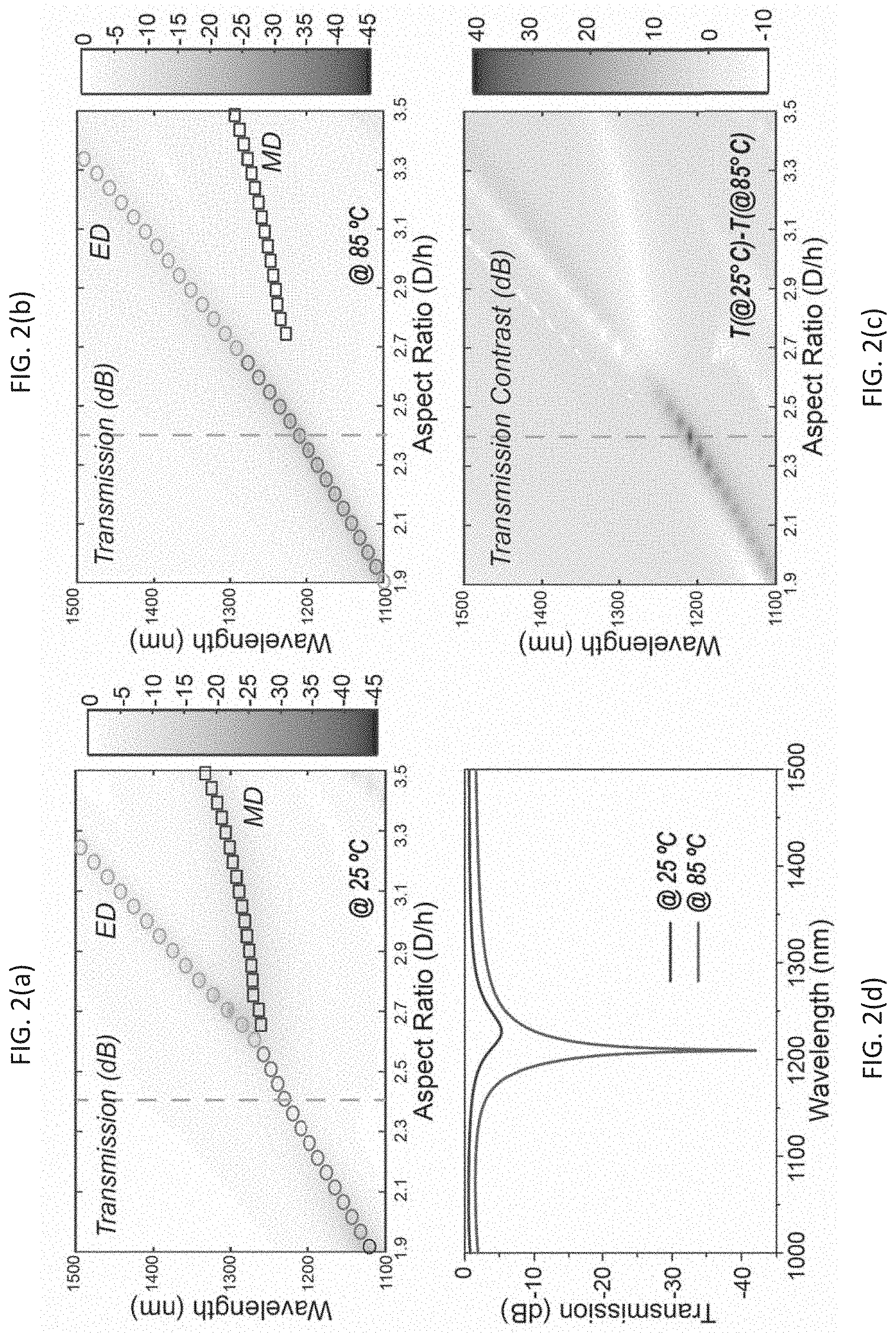
[0013] FIG. 2(a) shows aspect ratio (AR) of an exemplary device according to principles described herein at 25.degree. C.
[0014] FIG. 2(b) shows aspect ratio (AR) of an exemplary device according to principles described herein at 85.degree. C.
[0015] FIG. 2(c) shows transmission spectrum with AR=2.4.
[0016] FIG. 2(d) shows transmission contrast between on-state and off-state with different AR.
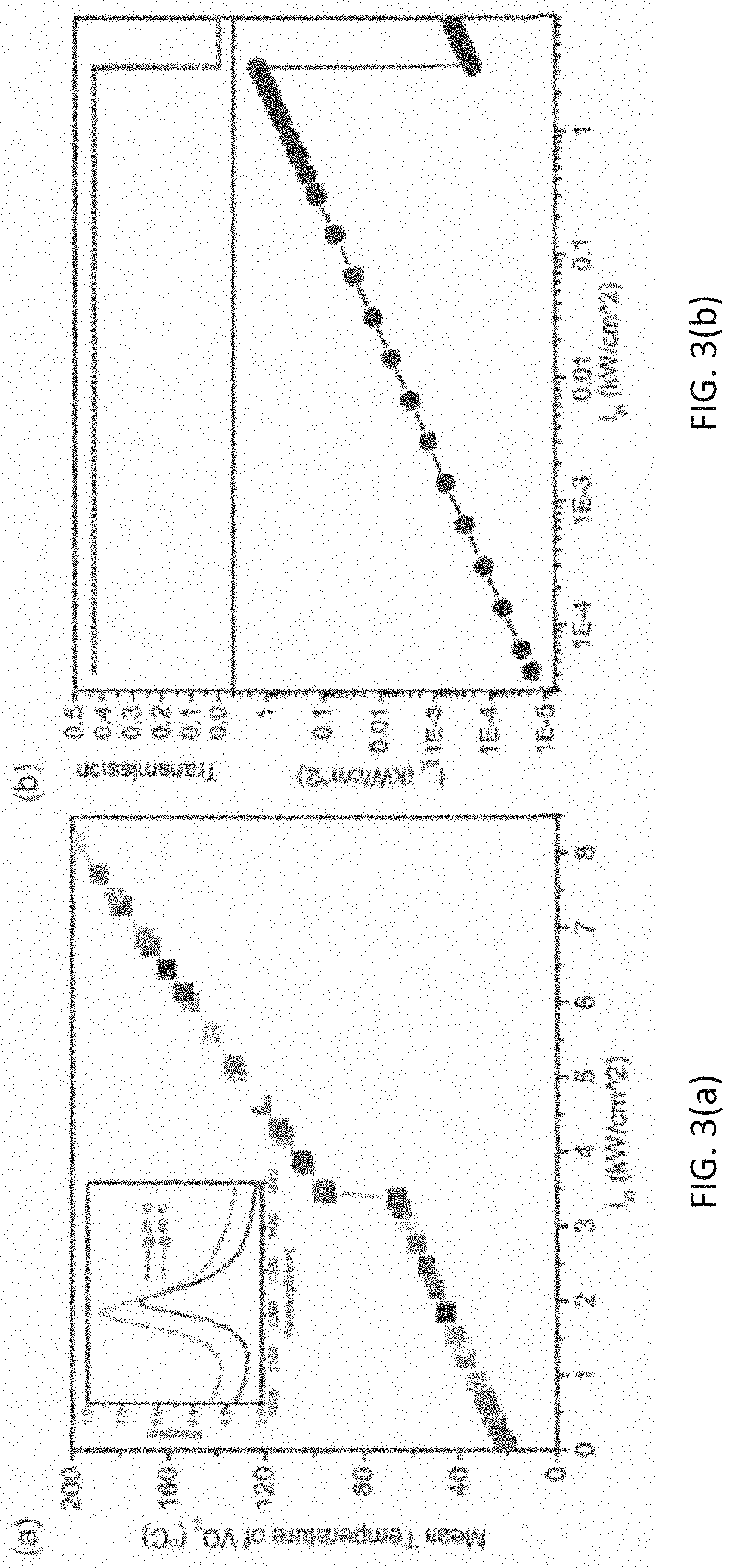
[0017] FIG. 3(a) shows a simulated mean temperature of the VO.sub.2 nanostructure under different incident intensity.
[0018] FIG. 3(b) shows a nonlinear relation between the transmission of the optical limiter and input intensity (top panel), output intensity I.sub.out and input intensity I.sub.in (bottom panel).
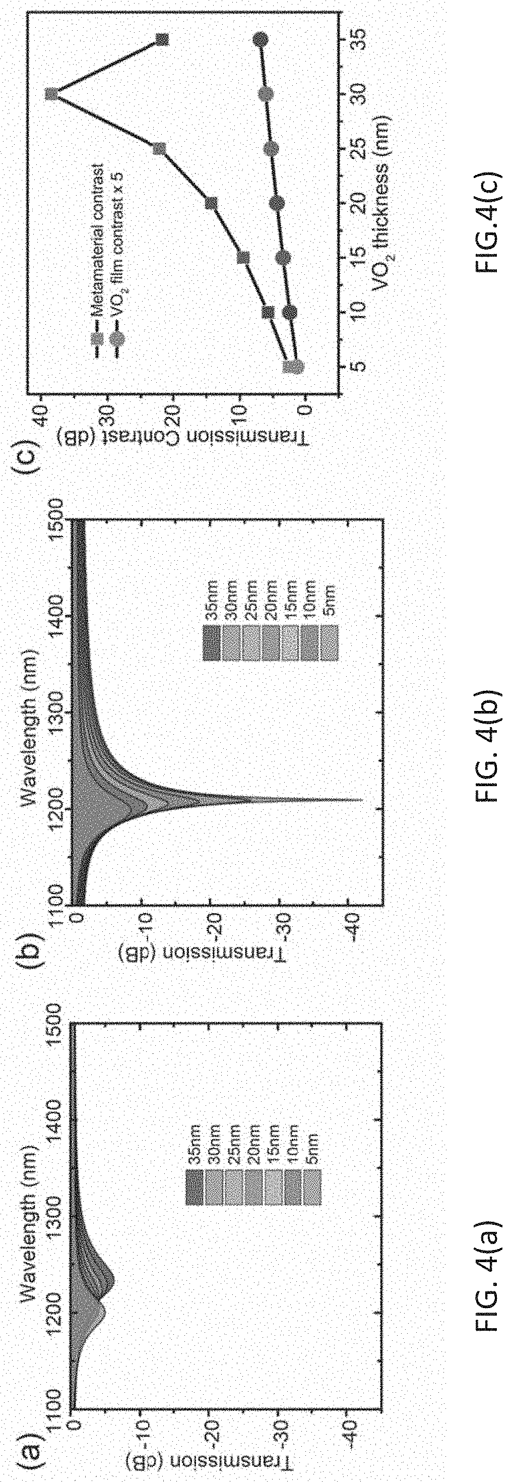
[0019] FIG. 4(a) shows a simulated transmission spectra with semiconducting phase VO.sub.2 as a function of film thickness.
[0020] FIG. 4(b) shows a simulated transmission spectra with metallic phase VO.sub.2.
[0021] FIG. 4(c) shows simulated transmission contrast with varying VO.sub.2 thickness for the Huygens metasurface-based optical limiter (solid square) and VO.sub.2 continuous film on SiO.sub.2 substrate (solid circle).
[0022] FIG. 5 shows experimental (parts (a) and (c) on the left of FIG. 5) and simulated experimental (parts (b) and (d) on the right of FIG. 5) performance of a device as described herein.
[0023] FIG. 6 shows simulated transmission spectra for Huygens metasurface-based optical limiter scaled to different wavelengths.
DETAILED DESCRIPTION
[0024] Reference will now be made in detail to embodiments of the optimal limiter using a metasurface and phase-change material with reference to the accompanying figures. The same reference numbers in different drawings may identify the same or similar elements.
[0025] At low intensities, the light is intended to pass through an optical limiter so that it can be recorded or imaged. Optical limiters that that will cause the device to become reflective or absorptive once the light fluence reaches a certain threshold are desirable, but creating a device that achieves limiting, while also being highly transmissive at low fluences has proven challenging. In the past twenty years, metamaterials and two-dimensional metasurfaces have assisted in optical dispersion engineering and enhancing light-matter interaction in communications, bio-sensing, super-resolution imaging and energy harvesting. All-dielectric metamaterials are most suitable for transmissive optics due to the low loss when working below the dielectrics' bandgaps. This feature has been used in high-efficiency optical systems such as metalenses, optical power switches, and polarization filters, which are difficult to achieve with plasmonic nanostructures in the visible and near infrared wavelength regime. Optical modulators and polarizers using liquid crystals, ultrafast switches using direct-bandgap semiconductors and graphene, and tunable reflectors with phase-change materials have all been made by combining active materials with metasurfaces, but no practical optical limiter has been produced to date.
[0026] An optical limiter according to principles described herein includes a phase-change material on a resonator. An example optical limiter may be made by integrating a phase-change material such as Vanadium Dioxide (VO.sub.2) with metamaterial all-dielectric nanostructures is described herein. In an optical limiter according to principles described herein, a Huygens metasurface may been implemented to get resonances with concentrated field distribution, as well as high on-state transmission T.sub.on. Then, an epsilon-near-zero (ENZ) mode may be introduced to damp down the off-state transmission T.sub.off.
[0027] An incident intensity cutoff point and the interrelationship between the performance and the volume of the VO.sub.2 have been studied and analyzed to produce an example of the proposed optical limiter with an optimized aspect ratio (AR) of the all-dielectric resonators. As described herein, a working wavelength can be accommodated across the near infrared by scaling the geometric parameters. Implementation of an optical limiter according to principles described herein could reasonably lead to highly secured real-time detection and sensing with minimizing or managing overheating and damage.
[0028] In an aspect, according to principles described herein, a device having a periodic nanostructure array of silicon and VO.sub.2 cylinders may be embedded in or on an insulating substrate, such as SiO.sub.2. A schematic of an exemplary unit cell of such a nanostructure array is illustrated in FIG. 1(a).
[0029] Dielectric resonators support resonant modes that are spectrally dependent on the dimensions of the structures. In an example, the lowest order Mie resonances, the electric dipole (ED) and magnetic dipole (MD) resonances may be spectrally overlapped at a resonance wavelength .lamda..sub.0 of 1209 nm. At this wavelength, the reflected fields from the two dipole modes are out of phase with one another, resulting in zero (or substantially zero) reflected intensity and unity (or substantial unity) transmission. This unique combination of dipole modes is known as a Huygens metasurface, which may be incorporated in to an optical limiter, as described herein. The transmission efficiency of the optical limiter will depend on whether the VO.sub.2 is in the semiconducting or metallic state and is expressed by T=1-|Im(VO.sub.2).times.E.sub.VO.sub.2.sup.2)|, where Im(VO.sub.2) and E.sub.VO.sub.2 are the imaginary part of the permittivity and electric field of the VO.sub.2, respectively. From the measured permittivity given in FIG. 1(b), the metallic phase VO.sub.2 (at 85.degree. C.) exhibits a larger imaginary permittivity than in the semiconducting state. This fulfills the basic requirement of an absorptive optical limiter--the device may be self-adjusted from on-state to off-state when the VO.sub.2 material is heated up above the phase transition threshold through light absorption.
[0030] FIG. 1(a) shows a schematic of an exemplary Huygens metasurface-based optical limiter according to principles described herein. As illustrated, in the example device, the diameter of the cylinder is D=432 nm, the height of silicon h=180 nm and thickness of VO.sub.2 t.sub.VO.sub.2=30 nm. The pitch p between each unit cell is substantially identical in both x and y directions, with p=640 nm in the present example device. FIG. 1(b) shows measured permittivity of 60 nm VO.sub.2 film on Si substrate at 25.degree. C. (black, completely semiconducting phase) and 85.degree. C. (purple, completely metallic phase); in FIG. 1(b) the real part is plotted with solid curve and imaginary part plotted with dash curve. FIG. 1(c) shows an electric field distribution in the z direction in a simulated electric field. The electric field is normalized to the incident Exo.
[0031] To better suppress the transmission of the off-state, an epsilon-near-zero (ENZ) mode may introduced. According to electromagnetic boundary conditions, the displacement current will be continuous across the Si--VO.sub.2 material interface, expressed by .epsilon..sub.SiE.sub.z_Si=.epsilon..sub.VO.sub.2E.sub.z_VO.sub.2. When the permittivity of VO.sub.2 approaches zero, the electric field inside the VO.sub.2 is enhanced to compensate. The E.sub.z field is given in FIG. 1(c), which illustrates that an enhancement factor of 8 is obtained by incorporating the ENZ mode into the device.
[0032] The transmission of the device as a function of wavelength and aspect ratio (AR) are displayed in FIGS. 2(a) and 2(b), which were simulated with commercial FDTD software--CST Microwave Studio. FIG. 2 shows calculated transmission of a Huygens metasurface-based optical limiter with different AR with semiconducting phase VO.sub.2 in FIG. 2(a) and metallic phase VO.sub.2 in FIG. 2(b). A dashed line indicates of the optimized AR, and symbols are used to trace the fundamental resonant modes ED (electric dipole) and MD (magnetic dipole). FIG. 2(c) shows transmission spectra at AR=2.4. Black and gray solid lines refer to Huygens metasurface-based optical limiter with semiconducting and metallic VO.sub.2 on the top, respectively. FIG. 2(d) shows transmission contrast between on-state and off-state with different AR.
[0033] The electric dipole (ED) and magnetic dipole (MD) resonance positions are initially spectrally separated, then gradually merge as the AR is decreased until they completely overlap at AR=2.4. Transmission spectra at AR=2.4 are plotted in FIG. 2(c) for better clarification. With this optimized AR, a high transmission of -3.6 dB is observed at the resonance wavelength of 1209 nm with semiconducting VO.sub.2 on top (FIG. 2(a)) due to equal strength of the scattering cross sections of the two resonances. When VO.sub.2 is heated and the transition to the metallic state occurs (FIG. 2(b)), the field enhancement in the VO.sub.2 generates absorption, and is observed as a decrease in transmittance to -41.8 dB. The transmittance contrast between the on-state and the off-state is 38.2 dB. This large contrast is expected to be the optimal value, which can be determined from the transmission contrast mapping in FIG. 2(d). If we continue to decrease the AR, the ED and MD should depart from each other, which is not discernable in the present dB plot.
[0034] To characterize the performance of the optical limiter and estimate the intensity threshold when it turns from on-state to off-state, a CST thermal solver is used here to calculate the mean temperature of the VO.sub.2 nanoparticles, using material properties listed in Table 1, below, which shows the thermal property of the materials in the Huygens metasurface-based on optical limiter according to principles described herein.
TABLE-US-00001 TABLE 1 Density Thermal Cond. Heat Capacity Materials (g/cm3) (W/K m) (kJ/K kg) Si 2.328 1.5 0.71 SiO2 2.4 1.4 0.75 VO.sub.2 (25.degree. C.) 4.57 3.5 0.656 VO.sub.2 (85.degree. C.) 4.64 6 0.78
[0035] FIG. 3(a) shows a simulated mean temperature of the VO.sub.2 nanostructure under different incident intensity. FIG. 3(b) shows a nonlinear relation between the transmission of the optical limiter and input intensity (top panel), output intensity I.sub.out and input intensity I.sub.in (bottom panel). Assuming silicon and SiO.sub.2 are both lossless, the injected power Q=A.times.I.sub.in.times..alpha. is entirely absorbed within the VO.sub.2 nanoparticles, where A is the cross-sectional area of the unit cell, I.sub.in is the incident intensity, and .alpha. is the absorption of the device. The absorption at the semiconducting and metallic VO.sub.2 state at .lamda.=1209 nm is .alpha..sub.25 .degree. C.=0.567 and .alpha..sub.85.degree. C.=0.898, respectively, as seen in FIG. 3(a). The VO.sub.2 film in the model is treated as a heat source that dissipates energy to its environment with an ambient air convection of 50 W/m.sup.2/K. Adiabatic boundaries were used in the in-plane directions to mimic a periodic boundary condition. In the semiconducting phase, the mean temperature of VO.sub.2 is heated to 67.degree. C. at an incident intensity of 3.4 kW/cm.sup.2 (FIG. 3(a)). Once the phase transition is triggered by an incident laser beam, the temperature will rise at a greater rate (include actual number here) due to the increased absorption, resulting in a drop in transmission (FIG. 3(b)). We observe a simulated decrease of 4 orders of magnitude in transmittance intensity I.sub.out, as seen in FIG. 3(b).
[0036] The intensity needed to activate the phase transition is around 3.4 kW/cm.sup.2 per unit cell (FIG. 3(a)). For example, for a 20 .mu.m.times.20 .mu.m device array, the required beam power is 13.6 mW, which is consistent with the fluence needed for ultrafast VO.sub.2 phase transition trigged by a femtosecond laser. This method requires less power to trigger the phase transition of VO.sub.2 than thermal heating since the dielectric environment surrounding the film experiences nearly zero absorption losses. Therefore, substantially all the absorbed incident power is funneled into the VO.sub.2 and more efficiently governs the material state than plasmonic metamaterials, in which metallic elements absorb a large amount of incident energy. In addition, metallic nanostructures possess a higher conductivity compared to dielectric environment in the present exemplary device, and exposure to air can also affect the thermal properties due to convection. FIG. 3(a) and FIG. 3(b) show simulated results.
[0037] The performance of the optical limiter is sensitive to the VO.sub.2 active layer thickness. If the VO.sub.2 is too thick, the on-state transmission may be reduced and the cutoff contrast harmed. If the VO.sub.2 is too thin, there may not be enough material to suppress the off-state transmission, even with the electric field enhancement from the resonator underneath. Additionally, the ENZ mode behavior relies on the thickness of the ENZ material. To illustrate this combined consequence on how the VO.sub.2 thickness affects the transmission and contrast, numerical simulations were performed with the same geometry as FIG. 1(a), while varying the VO.sub.2 thickness from 5 nm to 35 nm. The VO.sub.2 thickness dependence plots in FIGS. 4(a) and 4(b) demonstrate that the metamaterial transmission first decreases with thicker VO.sub.2. Different thicknesses of the metamaterial, such as VO.sub.2 may be used to make an optical limiter according to principles described herein provided that the resulting characteristics are acceptable for the contemplated use.
[0038] FIG. 4(a) shows a simulated transmission spectra with semiconducting phase VO.sub.2 as a function of film thickness. FIG. 4(b) shows a simulated transmission spectra with metallic phase VO.sub.2. FIG. 4(c) shows simulated transmission contrast with varying VO.sub.2 thickness for the Huygens metasurface-based optical limiter (solid square) and VO.sub.2 continuous film on SiO.sub.2 substrate (solid circle). The data of the VO.sub.2 continuous film is multiplied by a factor of 5 for better clarification. As can be seen in FIG. 4, the off-state exhibits a lower transmittance due to the increased loss in metallic phase VO.sub.2. When the thickness is increased to 35 nm, the transmittance contrast begins to decrease, indicating that an optimal VO.sub.2 thickness is 30 nm. This value is based on the coupling condition between the ED and MD, as well as the high dispersion of the ENZ. For thicker VO.sub.2, though the dimension of the resonators can be modified to retrieve best overlap of ED and MD, the operation wavelength may be tuned away and the contribution from ENZ mode enabled field enhancement may be eliminated. To emphasize the field enhancement from the dielectric resonators, simulations of the transmission on VO.sub.2 films were performed, with the same thicknesses given in FIGS. 4(a) and 4(b). Since the films do not benefit from the Huygens mode fields in a nearby resonator, the on-off contrast is reduced by 37.0 dB compared to the metasurface design (FIG. 4(c)). FIG. 5 shows experimental (parts (a) and (c) on the left of FIG. 5) and simulated experimental (parts (b) and (d) on the right of FIG. 5) performance of device as described herein.
[0039] One advantage of this metasurface-based design is the ability to adjust the working wavelength by tuning the size of the resonators. With the standard carrier concentration used in the exemplary device above, the ENZ point of the VO.sub.2 thin films is 1200 nm. Despite the fact that the ENZ point is fixed, it is possible to achieve high transmittance contrast between the on state and the off-state of the device at longer wavelengths where metallic VO.sub.2 has larger absorption losses. To explore how this type of metasurface operates at other wavelengths, devices were simulated with unit cell dimensions scaled by a factor of s with the exception of the VO.sub.2 thickness, which is held constant at 30 nm. FIG. 6 shows simulated transmission spectra for Huygens metasurface-based optical limiter scaled to different wavelengths. The overall geometry is equally adjusted with a scale s=0.9, 1.1, 1.3 and 1.5 to work near 1064 nm, 1350 nm, 1550 nm, and 1850 nm, respectively. Over 20 dB on-off transmittance contrast is observed for all four scaled metasurfaces, compared to 38.2 dB transmittance contrast for a device with s=1. The decreased contrast for the scaled designs illustrates that the spectral location of the ENZ mode governs the magnitude of field concentration in the VO.sub.2 film and controls the cutoff efficiency.
[0040] Described herein is a metasurface-based optical limiter working in the near infrared region. To enhance the interaction between the incident light and VO.sub.2 thin film, a Huygens mode is created in the supporting Si resonator by overlapping the electric and magnetic Mie dipole modes. By designing the Huygens mode spectrally near the ENZ point of the VO.sub.2 film, the field inside the VO.sub.2 is enhanced to increase absorptance. By controlling the phase of the VO.sub.2 film, the transmittance of the device can be adjusted by tuning the coupling of the ENZ point of the VO.sub.2 and the Huygens mode of the resonators. A transmittance contrast of 38.2 dB has been demonstrated experimentally, which exhibited superior performance to a continuous VO.sub.2 film of the same thickness. The optical limiter performance has been systemically analyzed using a thermal solver and an intensity threshold of 3.4 kW/cm2 is predicted. This threshold can be adjustable with doping or applied external stress. Additionally, we show that the working wavelength is tunable across the near-IR by altering the scale of the unit cell dimensions. This metasurface-based design serves as a strong alternative for free space or on-chip optical limiters.
[0041] While the exemplary embodiment described herein uses VO.sub.2 as the phase-change material, an optical limiter according to principles described herein may include other phase-change materials in place or in addition to VO.sub.2, including, but not limited to Tin Oxides, Gallium Phosphides, Germanium, Gallium Arsenides, Gallium Nitrides, and/or other phase-change materials with a refractive index of 1.5 or greater. In some embodiments, the refractive index of the phase-change material may be greater than 2. While optical limiters described herein are formed on an Si resonator, other materials may be used in place of the Si to provide an appropriate resonator, such as titanium dioxide, gallium phosphide, gallium nitride, and gallium arsenide.
[0042] Optical limiters as described herein may be used in various applications, including, but not limited to, eyewear for protection from laser exposure. This would be appropriate for the military or civilian market. The civilian market could include individuals working with lasers as well as pilots and private security. The optical limiter as described herein can also be used in protecting any camera, machine vision focal plane array, pixel sensor (including single pixel sensors), charge coupled device, or the like. The array configuration can be scaled for larger applications, such as windows, windshields, and the like. Appropriate substrate materials may be chosen according to the application.
[0043] A transmissive and all-dielectric optical limiter with great cutoff efficiency using Vanadium Dioxide (VO.sub.2) as the active component is disclosed. Vanadium dioxide may be chosen for an optical limiter due to the large contrast in optical constants upon undergoing the semiconductor to metal phase transition. When triggered optically, this transition occurs within 60 fs, making the device suitable for an ultrafast laser environment. In addition, the phase transition threshold is tunable by applying stress or doping; therefore, the device cutoff intensity can be adjusted to fulfill specific requirements.
[0044] Optical limiters are designed to limit the intensity of light at high fluences. This is typically done to protect electronics or an individual's eyes from exposure to intense and damaging laser light. In some aspects of the present device, at low intensities the light may pass through the limiter so that it can be recorded or imaged. The device may contain some nonlinear material that will cause the device to become reflective or absorptive once the light fluence reaches a certain threshold. Generally, sacrifices may be made in the low fluence transmission at, or around, the limiting wavelength or in the level to which the device limits the transmission at high fluence. Nonlinear materials may be integrated with artificial materials to form an optical limiter.
[0045] In this work we have designed a structured material, hereby referred to as a metasurface, to realize an optical limiter that is both highly transmissive at low fluence while having a large optical density (OD), or low transmission, at high fluence. The metasurface comprises an array of optical resonators that are formed from structuring a dielectric material such as silicon or titanium dioxide. According to and aspect described herein, the metasurface is design by overlapping electric and magnetic dipole resonances. This allows for unity transmission at the optical resonance while still concentrating energy in the resonator material. A thin layer of phase-change media, or any other active media whose optical properties will change at high fluence, is placed on top of the resonator. When fluence reaches a certain level, the active material's properties change causing transmission to significantly dip at the resonance frequency, providing limiting.
[0046] In one configuration of the device the active material is designed to work at a wavelength where its electrical permittivity is zero in either the low or high fluence state. This is referred to as the epsilon-near-zero (ENZ) point and allows the use of thinner active media due to field concentration in the active medium. However, operating at the ENZ point is not necessary. Vanadium dioxide (VO.sub.2) may be used as the active medium and silicon as the resonator. VO.sub.2 undergoes a semiconductor to metal phase transition at .about.67.degree. C. which causes a large change in its electrical permittivity. In the current implementation the VO.sub.2 will transition to the metallic phase at high fluence due to heating. This transition causes a large increase in absorption and a subsequent dip in the transmission. The low fluence transmission is roughly -5 dB at the resonance frequency with a high fluence transmission less than -40 dB based on at least one contemplated design.
[0047] An optical device according to principles described herein may be formed according to known fabrication techniques, including but not limited to, photolithography, electron beam lithography, nanoimprint lithography, self-assembly-based patterning, colloidal synthesis, and screen printing.
[0048] A number of embodiments of the disclosure have been described. Nevertheless, it will be understood that various modifications may be made without departing from the spirit and scope of the invention. Accordingly, other embodiments are within the scope of the following claims.
[0049] While various embodiments of the present invention have been described above, it should be understood that they have been presented by way of example only, and not limitation. It will be apparent to persons skilled in the relevant art that various changes in form and detail can be made therein without departing from the spirit and scope of the present invention. Thus, the breadth and scope of the present invention should not be limited by any of the above-described exemplary embodiments, but should be defined only in accordance with the following claims and their equivalents.
* * * * *
D00000
D00001
D00002
D00003
D00004
D00005
D00006
XML
uspto.report is an independent third-party trademark research tool that is not affiliated, endorsed, or sponsored by the United States Patent and Trademark Office (USPTO) or any other governmental organization. The information provided by uspto.report is based on publicly available data at the time of writing and is intended for informational purposes only.
While we strive to provide accurate and up-to-date information, we do not guarantee the accuracy, completeness, reliability, or suitability of the information displayed on this site. The use of this site is at your own risk. Any reliance you place on such information is therefore strictly at your own risk.
All official trademark data, including owner information, should be verified by visiting the official USPTO website at www.uspto.gov. This site is not intended to replace professional legal advice and should not be used as a substitute for consulting with a legal professional who is knowledgeable about trademark law.