Devices And Methods For Photoelectrochemical Water Splitting
Steiner; Myles Aaron ; et al.
U.S. patent application number 16/580179 was filed with the patent office on 2020-04-16 for devices and methods for photoelectrochemical water splitting. The applicant listed for this patent is Alliance for Sustainable Energy, LLC. Invention is credited to Isabel Barraza Alvarez, Todd Gregory Deutsch, Daniel Joseph Friedman, John David Simon, Myles Aaron Steiner, James Luke Young.
| Application Number | 20200115810 16/580179 |
| Document ID | / |
| Family ID | 70161205 |
| Filed Date | 2020-04-16 |


View All Diagrams
| United States Patent Application | 20200115810 |
| Kind Code | A1 |
| Steiner; Myles Aaron ; et al. | April 16, 2020 |
DEVICES AND METHODS FOR PHOTOELECTROCHEMICAL WATER SPLITTING
Abstract
The present disclosure relates to a photoelectrochemical electrode that includes an absorber layer having a quantum well, where the photoelectrochemical electrode is configured to perform a first reaction defined as, 4H.sup.-+4e.sup.-2H.sub.2, or a second reaction defined as, 2H.sub.2OO.sub.2+4H.sup.++4e.sup.-, when the photoelectrochemical electrode is configured to be in contact with water.
| Inventors: | Steiner; Myles Aaron; (Denver, CO) ; Friedman; Daniel Joseph; (Lakewood, CO) ; Simon; John David; (Austin, TX) ; Deutsch; Todd Gregory; (Arvada, CO) ; Young; James Luke; (Golden, CO) ; Alvarez; Isabel Barraza; (Santa Barbara, CA) | ||||||||||
| Applicant: |
|
||||||||||
|---|---|---|---|---|---|---|---|---|---|---|---|
| Family ID: | 70161205 | ||||||||||
| Appl. No.: | 16/580179 | ||||||||||
| Filed: | September 24, 2019 |
Related U.S. Patent Documents
| Application Number | Filing Date | Patent Number | ||
|---|---|---|---|---|
| 62743977 | Oct 10, 2018 | |||
| 62754689 | Nov 2, 2018 | |||
| 62836138 | Apr 19, 2019 | |||
| Current U.S. Class: | 1/1 |
| Current CPC Class: | C25B 11/0478 20130101; C25B 1/003 20130101; C25B 11/0405 20130101; C25B 1/04 20130101 |
| International Class: | C25B 11/04 20060101 C25B011/04; C25B 1/00 20060101 C25B001/00; C25B 1/04 20060101 C25B001/04 |
Goverment Interests
CONTRACTUAL ORIGIN
[0002] The United States Government has rights in this disclosure under Contract No. DE-AC36-08G028308 between the United States Department of Energy and the Alliance for Sustainable Energy, LLC, the Manager and Operator of the National Renewable Energy Laboratory.
Claims
1. A photoelectrochemical electrode comprising: an absorber layer comprising a quantum well, wherein: the photoelectrochemical electrode is configured to perform a first reaction defined as, 4H.sup.++4e.sup.-2H.sub.2, or a second reaction defined as, 2H.sub.2OO.sub.2+4H.sup.++4e.sup.-, when the photoelectrochemical electrode is configured to be in contact with water.
2. The photoelectrochemical electrode of claim 1, wherein: the quantum well comprises, in order: a first barrier layer having a first bandgap; a well layer having a second bandgap; and a second barrier having a third bandgap, wherein; the second bandgap is less than the first bandgap and the third bandgap.
3. The photoelectrochemical electrode of claim 2, wherein: the first bandgap and the third bandgap are between about 1.4 eV and about 1.66 eV, inclusively, and the second bandgap is between about 1.13 and about 1.4 eV, inclusively.
4. The photoelectrochemical electrode of claim 3, wherein: the first barrier layer and the second barrier both comprise GaAs.sub.1-yP.sub.y, and y is between about 0.0 and about 0.2, inclusively.
5. The photoelectrochemical electrode of claim 3, wherein: the well layer comprises Ga.sub.1-xIn.sub.xP, and x is between about 00.0 and about 0.2, inclusively.
6. The photoelectrochemical electrode of claim 2, wherein: the first barrier layer and the second barrier layer have a thickness between about 1 nm and about 50 nm, and the well layer has a thickness between about 1 nm and about 20 nm.
7. The photoelectrochemical electrode of claim 1, wherein the absorber layer comprises between 1 and 100 quantum wells.
8. The photoelectrochemical electrode of claim 1, further comprising: a substrate layer; and a reflecting layer, wherein: the reflecting layer is positioned between the substrate and the absorber layer, and the reflecting layer is a Bragg reflector.
9. The photoelectrochemical electrode of claim 8, wherein the substrate is lattice-matched to the quantum well.
10. The photoelectrochemical electrode of claim 8, wherein the substrate is lattice-mismatched to the quantum well.
11. The photoelectrochemical electrode of claim 8, wherein: the Bragg reflector comprises: a first layer having a first index of refraction; and a second layer having a second index of refraction, wherein: the first index of refraction is different than the second index of refraction.
12. The photoelectrochemical electrode of claim 1, wherein both the first index of refraction and the second index of refraction are between 2.5 and 4.0, inclusively.
13. The photoelectrochemical electrode of claim 12, wherein: the first index of refraction is about 3.5, and the second index of refraction is about 3.0.
14. The photoelectrochemical electrode of claim 13, wherein: the first layer comprises GaAs, and the second layer comprises AlAs.
15. The photoelectrochemical electrode of claim 8, wherein: the absorber layer further comprises: a first doped layer, and a second doped layer, wherein: the quantum well is positioned between the first doped layer and the second doped layer, the second doped layer is positioned between the substrate and the second doped layer, and the second doped layer is the opposite doping of the first doped layer.
16. The photoelectrochemical electrode of claim 15, wherein: the first doped layer is p-type or n-type, the second doped layer is p-type or n-type, and the doping type of the second doped layer is the opposite of the doping type of the first doped layer.
17. The photoelectrochemical electrode of claim 16, wherein: the first doped layer and the second doped layer each have a bandgap between about 1.0 eV and about 1.5 eV, inclusively.
18. The photoelectrochemical electrode of claim 17, wherein: both the first doped layer and the second doped layer comprise Al.sub.xGa.sub.yIn.sub.zAs.sub.vP.sub.wN.sub.tSb.sub.u, x is between 0.0 and 1.0, y is between 0.0 and 1.0, z is between 0.0 and 1.0, v is between 0.0 and 1.0, w is between 0.0 and 1.0, t is between 0.0 and 1.0, u is between 0.0 and 1.0, and x+y+z=u+t+v+w=1.0.
19. The photoelectrochemical electrode of claim 18, wherein at least one of the first doped layer or the second doped layer comprises GaAs.
20. The photoelectrochemical electrode of claim 15, further comprising: a second absorber layer, wherein: the absorber layer having the quantum well is positioned between the reflecting layer and the second absorber layer.
Description
CROSS-REFERENCE TO RELATED APPLICATIONS
[0001] This application claims the benefit of U.S Provisional Patent Application Nos. 62/743,977, 62/754,689, and 62/836,138 filed Oct. 10, 2018, Nov. 2, 2018, and Apr. 19, 2019, respectively, the contents of which are incorporated herein by reference in their entirety.
BACKGROUND
[0003] Water splitting refers to the chemical reaction of water to its constituent elements in the form of diatomic hydrogen and diatomic oxygen. Photoelectrochemical (PEC) water splitting is a promising pathway to the economical production of solar hydrogen. Using a semiconductor to directly split water eliminates the high capital costs of an electrolyzer. The key parameters that dictate hydrogen costs from the PEC approach are semiconductor efficiency, stability, and cost. Technoeconomic analysis for PEC hydrogen production reveals that high solar-to-hydrogen (STH) efficiency is the most critical figure of merit when designing such a system.
[0004] STH efficiency is proportional to the photocurrent generated by the device, as long as the voltage generated is sufficient to overcome the thermodynamic potential and any surface kinetic effects. The photocurrent in a PEC device depends on the number of absorbed photons per unit time. The absorption, and therefore the STH efficiency, can be increased by extending the wavelength range of photon absorption.
[0005] The baseline standard for a PEC device is a GaInP/GaAs tandem cell, grown lattice-matched on a GaAs substrate. This cell absorbs light with wavelengths less than approximately 870 nm. One technique for extending the absorption range is to use a semiconductor "dilute-nitride-antimonide" alloy GaInAsNSb lattice-matched to GaAs and containing small amounts of nitrogen (N) and/or antimony (Sb) for the bottom junction absorber layer. This approach has the drawback that these alloys are very difficult to grow with the required optoelectronic quality. Another technique for extending the absorption range is to change the lattice constant to enable growth of a second absorber layer of GaInAs, with a lower bandgap but larger lattice constant than the substrate. The absorption range has been extended out to 1033 nm by devices incorporating this design feature. This metamorphic technique has demonstrated high efficiencies, but the cell is grown inverted and is more complicated to grow and process; requires removal of the substrate; and may not be compatible with some advanced processing techniques. Thus, there remains a need for improved PEC designs and systems that provide higher STH efficiencies to enable more affordable hydrogen production.
SUMMARY
[0006] An aspect of the present disclosure is a photoelectrochemical electrode that includes an absorber layer having a quantum well, where the photoelectrochemical electrode is configured to perform a first reaction defined as,
4H.sup.-+4e.sup.-2H.sub.2,
and/or a second reaction defined as,
2H.sub.2OO.sub.2+4H.sup.++4e.sup.-,
when the photoelectrochemical electrode is configured to be in contact with water.
[0007] In some embodiments of the present disclosure, the quantum well may include, in order, a first barrier layer having a first bandgap, a well layer having a second bandgap, and a second barrier having a third bandgap, where the second bandgap is less than the first bandgap and the third bandgap. In some embodiments of the present disclosure, the first bandgap and the third bandgap may be between 1.4 eV and 1.66 eV, inclusively, and the second bandgap may be between 1.13 and 1.4 eV, inclusively. In some embodiments of the present disclosure, the first barrier layer and the second barrier may both include GaAs.sub.1-yP.sub.y, where y may be between about 0 and about 0.2, inclusively. In some embodiments of the present disclosure, the well layer may include Ga.sub.1-xIn.sub.xP, where x may be between about 0 and about 0.2, inclusively. In some embodiments of the present disclosure, the first barrier layer and the second barrier layer may have a thickness between about 1 nm and about 50 nm, and the well layer may have a thickness between about 1 nm and about 20 nm. In some embodiments of the present disclosure, the absorber layer may have between 1 and 100 quantum wells.
[0008] In some embodiments of the present disclosure, the photoelectrochemical electrode may further include a substrate layer, and a reflecting layer, where the reflecting layer is positioned between the substrate and the absorber layer, and the reflecting layer is a Bragg reflector. In some embodiments of the present disclosure, the substrate may be lattice-matched to the quantum well. In some embodiments of the present disclosure, the substrate may be lattice-mismatched to the quantum well. In some embodiments of the present disclosure, the Bragg reflector may include a first layer having a first index of refraction, and a second layer having a second index of refraction, where the first index of refraction is different than the second index of refraction. In some embodiments of the present disclosure, both the first index of refraction and the second index of refraction may be between 2.5 and 4.0, inclusively. In some embodiments of the present disclosure, the first index of refraction may be about 3.5, and the second index of refraction may be about 3.0. In some embodiments of the present disclosure, the first layer may include GaAs, and the second layer may include AlAs.
[0009] In some embodiments of the present disclosure, the absorber layer may further include a first doped layer, and a second doped layer, where the quantum well is positioned between the first doped layer and the second doped layer, the second doped layer is positioned between the substrate and the second doped layer, and the second doped layer is the opposite doping of the first doped layer. In some embodiments of the present disclosure, the first doped layer may be p-type or n-type, the second doped layer may be p-type or n-type, the doping type of the second doped layer is the opposite of the doping type of the first doped layer. In some embodiments of the present disclosure, the first doped layer and the second doped layer may each have a bandgap between about 1.0 eV and about 1.5 eV, inclusively. In some embodiments of the present disclosure, both the first doped layer and the second doped layer may include Al.sub.xGa.sub.yIn.sub.zAs.sub.vP.sub.wN.sub.tSb.sub.u, where x is between 0.0 and 1.0, y is between 0.0 and 1.0, z is between 0.0 and 1.0, v is between 0.0 and 1.0, w is between 0.0 and 1.0, t is between 0.0 and 1.0, u is between 0.0 and 1.0, and x+y+z=u+t+v+w=1.0 In some embodiments of the present disclosure, at least one of the first doped layer or the second doped layer may include GaAs.
[0010] In some embodiments of the present disclosure, photoelectrochemical electrode may further include a second absorber layer, where the absorber layer having the quantum well is positioned between the reflecting layer and the second absorber layer. In some embodiments of the present disclosure, the second absorber layer may have a bandgap that is greater than the bandgap of the first doped layer and the second doped layer. In some embodiments of the present disclosure, the bandgap of the second absorber layer may be between about 1.5 eV and about 1.9 eV, inclusively. In some embodiments of the present disclosure, the second absorber layer may include an alloy of GaInP. In some embodiments of the present disclosure, the second absorber layer may further include an n-doped layer and a p-doped layer.
DRAWINGS
[0011] Exemplary embodiments are illustrated in referenced figures of the drawings. It is intended that the embodiments and figures disclosed herein are to be considered illustrative rather than limiting.
[0012] FIG. 1 illustrates a photoelectrochemical device for capturing solar energy and utilizing the energy captured toward water electrolysis to produce H.sub.2 and O.sub.2, according to some embodiments of the disclosure.
[0013] FIG. 2 illustrates a first electrode of the photoelectrochemical device of FIG. 1, according to some embodiments of the present disclosure.
[0014] FIG. 3 illustrates an absorber layer of the first electrode of FIG. 2, according to some embodiments of the present disclosure.
[0015] FIG. 4 illustrates a first electrode of the photoelectrochemical device of FIG. 1, according to some embodiments of the present disclosure.
[0016] FIG. 5A illustrates a schematic of the tandem solar cell device, including the QW region and a 20-layer Bragg reflector, according to some embodiments of the present disclosure. Some devices in this disclosure exclude one or both of those layer sets.
[0017] FIG. 5B illustrates an isolated PEC electrode, with SU-8 isolating the mesa, epoxy protecting the cleaved sidewalls, and copper foil electrical contact to the back, according to some embodiments of the present disclosure.
[0018] FIG. 5C illustrates photographs of PV (top) and PEC (bottom) devices, according to some embodiments of the present disclosure. The PV device shows 4 cells and a Hall bar; the PEC device shows a single device.
[0019] FIG. 6A illustrates the external quantum efficiency (EQE) of PV devices, according to some embodiments of the present disclosure. The legend indicates the device name and some details of the device architecture.
[0020] FIG. 6B illustrates the incident photon to current efficiency (IPCE) of PEC, according to some embodiments of the present disclosure. The IPCE data appear slightly higher than the EQE of FIG. 6A because the aqueous electrolyte acts as an anti-reflection layer.
[0021] FIG. 7A illustrates the current-voltage curve for a PV device and FIG. 7B illustrates the current-voltage curve for a PEC device, according to some embodiments of the present disclosure. The PEC devices were measured in 0.5M sulfuric acid, with respect to an iridium oxide counter electrode. For both data sets, the intensity was set to 1000 W/m.sup.2 to simulate the AM1.5 reference spectrum. Some light is collimated in the PEC measurement, effectively increasing the concentration.
[0022] FIG. 8 illustrates short-circuit photocurrent of the four devices, at 0 V (red) and -0.5 V (blue) relative to an IrO.sub.x counter electrode, according to some embodiments of the present disclosure. Only curves that exhibited the light-limited photocurrent at 0 V were included in the analysis. The error bars indicate the standard deviation.
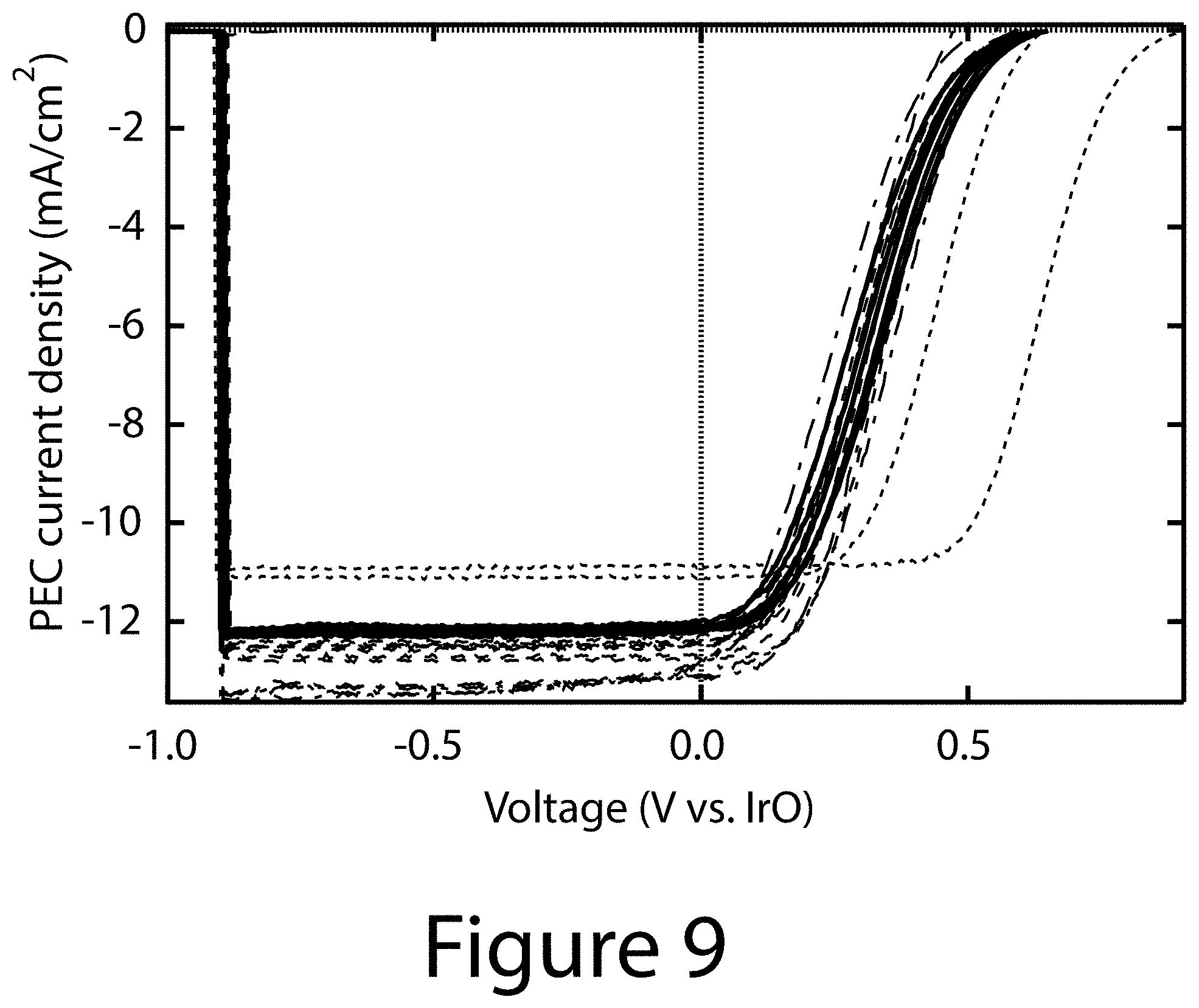
[0023] FIG. 9 illustrates a full set of JV curves for the PEC electrodes, according to some embodiments of the present disclosure. The line types are the same as in FIGS. 5 and 6.
REFERENCE NUMBERS
[0024] 100 . . . device
[0025] 110 . . . first electrode
[0026] 120 . . . second electrode
[0027] 130 . . . connector
[0028] 140 . . . membrane
[0029] 150 . . . electrolyte
[0030] 210 . . . Ohmic contact
[0031] 215 . . . tunnel junction
[0032] 220 . . . substrate layer
[0033] 230 . . . reflecting layer
[0034] 240 . . . passivation layer
[0035] 250 . . . first absorber layer
[0036] 260 . . . second absorber layer
[0037] 270 . . . capping layer
[0038] 280 . . . catalyst
[0039] 300 . . . quantum well
[0040] 310 . . . well layer
[0041] 320 . . . barrier layer
[0042] 330 . . . first doped layer
[0043] 340 . . . second doped layer
DETAILED DESCRIPTION
[0044] The present disclosure may address one or more of the problems and deficiencies of the prior art discussed above. However, it is contemplated that some embodiments as disclosed herein may prove useful in addressing other problems and deficiencies in a number of technical areas. Therefore, the embodiments described herein should not necessarily be construed as limited to addressing any of the particular problems or deficiencies discussed herein.
[0045] References in the specification to "one embodiment", "an embodiment", "an example embodiment", "some embodiments", etc., indicate that the embodiment described may include a particular feature, structure, or characteristic, but every embodiment may not necessarily include the particular feature, structure, or characteristic. Moreover, such phrases are not necessarily referring to the same embodiment. Further, when a particular feature, structure, or characteristic is described in connection with an embodiment, it is submitted that it is within the knowledge of one skilled in the art to affect such feature, structure, or characteristic in connection with other embodiments whether or not explicitly described.
[0046] As used herein the term "substantially" is used to indicate that exact values are not necessarily attainable. By way of example, one of ordinary skill in the art will understand that in some chemical reactions 100% conversion of a reactant is possible, yet unlikely. Most of a reactant may be converted to a product and conversion of the reactant may asymptotically approach 100% conversion. So, although from a practical perspective 100% of the reactant is converted, from a technical perspective, a small and sometimes difficult to define amount remains. For this example of a chemical reactant, that amount may be relatively easily defined by the detection limits of the instrument used to test for it. However, in many cases, this amount may not be easily defined, hence the use of the term "substantially". In some embodiments of the present invention, the term "substantially" is defined as approaching a specific numeric value or target to within 20%, 15%, 10%, 5%, or within 1% of the value or target. In further embodiments of the present invention, the term "substantially" is defined as approaching a specific numeric value or target to within 1%, 0.9%, 0.8%, 0.7%, 0.6%, 0.5%, 0.4%, 0.3%, 0.2%, or 0.1% of the value or target.
[0047] As used herein, the term "about" is used to indicate that exact values are not necessarily attainable. Therefore, the term "about" is used to indicate this uncertainty limit. In some embodiments of the present invention, the term "about" is used to indicate an uncertainty limit of less than or equal to .+-.20%, .+-.15%, .+-.10%, .+-.5%, or .+-.1% of a specific numeric value or target. In some embodiments of the present invention, the term "about" is used to indicate an uncertainty limit of less than or equal to .+-.1%, .+-.0.9%, .+-.0.8%, .+-.0.7%, .+-.0.6%, .+-.0.5%, .+-.0.4%, .+-.0.3%, .+-.0.2%, or .+-.0.1% of a specific numeric value or target.
[0048] For the reasons discussed in the previous paragraph, there are advantages to an upright, lattice-matched device compared to an inverted metamorphic device or a device employing dilute-nitride-antimonides as absorber layer(s). Thus, the present disclosure relates to the innovation of extending the absorption range of the bottom cell in the tandem PEC device out to longer wavelengths by including multiple quantum wells (MQWs) in the upright lattice-matched structure, thus increasing the efficiency while retaining the advantages of the upright lattice-matched structure. The MQWs can be lattice-matched or strain-balanced, but in either case the net strain is zero and the device remains lattice-matched. Quantum wells include a lower bandgap material sandwiched between higher bandgap barriers. The absorption edge of the well depends on the bandgaps of the well and barrier materials, and the thickness of the well layer.
[0049] Some embodiments of the disclosure described herein provide tandem absorber photoelectrochemical devices with very high water-splitting efficiencies. For example, FIG. 1 illustrates a photoelectrochemical device 100 for capturing solar energy and utilizing the captured energy for electrolysis to produce diatomic hydrogen and diatomic oxygen from water, according to the following reactions.
At the cathode (first electrode): 4H.sup.++4e.sup.-2H.sub.2 (1)
At the anode (second electrode): 2H.sub.2OO.sub.2+4H.sup.++4e.sup.- (2)
Total reaction: 2H2O2H.sub.2+O.sub.2 (3)
[0050] The photoelectrochemical device 100 may include a first electrode 110 and a second electrode 120 electrically linked together by a connector 130, for example, an electrically conductive wire such as copper, stainless steel, titanium, silver, gold, platinum, palladium, aluminum and/or any other suitable electrically conducting material. The first electrode 110 and the second electrode 120 may be immersed in a liquid electrolyte 150 contained in an appropriate vessel. In some embodiments, the container may include a membrane 140, which physically separates the first electrode 110 from the second electrode 120 and divides the electrolyte into two portions, 150A and 150B, with electrolyte 150A associated with the first electrode 110, and electrolyte 150B associated with the second electrode 120. In some embodiments, the container may be filled with an aqueous electrolyte that may be acidic, basic, or neutral. An aqueous electrolyte may be characterized by a pH ranging from greater than about 0 to about 14. In other embodiments, an aqueous electrolyte may be characterized by a pH ranging from greater than about -0.5 to about 7. An aqueous electrolyte may be an acid solution containing, for example, a strong acid such as HI, HBr, HClO.sub.4, HClO.sub.3, H.sub.2SO.sub.4, and/or HNO.sub.3. In some embodiments, the electrolyte may include a weak acid such as CH.sub.3COOH (acetic acid), HCOOH (formic acid), HF, HCN (hydrocyanic acid), and/or HNO.sub.2 (nitrous acid). Aqueous electrolytes may also include basic solutions that include, for example, KOH and/or NaOH solutions. Any other suitable acidic or basic solutions may be used.
[0051] A membrane 140 may be configured to only allow ions to pass through it, for example protons (W). In some embodiments, a membrane 140 may be porous. A membrane 140 may be configured to separate the electrolyte into two portions (150A and 150B), such that ions may be transported from one side of the membrane 140 and one portion of the electrolyte to the other side of the membrane and other portion of the electrolyte, while simultaneously preventing the reaction products (H.sub.2 and O.sub.2) from contacting each other. Examples of porous membranes include fluorinated polymers (e.g. Nafion.RTM., Flemion.RTM., Teflon.RTM., and Aciplex.RTM.), polyether-ether ketone (e.g. SPEEK.RTM.), poly(phenylquinoxalene) polymers, and/or copolymers thereof. Anion exchange membranes may also be used, for example, with basic electrolytes. Methods of making one or more of the films and/or layers of the devices described herein may include metal organic chemical vapor deposition (MOCVD), metal organic vapor phase epitaxy (MOVPE), molecular beam epitaxy (MBE), hydride vapor phase epitaxy (HVPE), chemical vapor deposition methods (CVD), liquid phase epitaxy (LPE), and/or other suitable methods.
[0052] In the example of FIG. 1, the first electrode 110, the cathode, absorbs light resulting in the formation of electrons (not shown) near the surface of the first electrode 110, which combine with the protons to form diatomic hydrogen per reaction (1). These electrons are replaced by the formation of electrons occurring at the anode according to reaction (2). These electrons flow through the connector 130 from the second electrode 120 to the first electrode 110 to maintain the electron balance, resulting in the total reaction (3). Referring again to FIG. 1, this example illustrates the case where the first electrode 110, receives and absorbs the light and operates as a photocathode. However, elements described herein apply generally to photoelectrochemical devices for both devices that utilize a photocathode and cases where the light-receiving electrode is the anode (photoanodes). The switch from a photocathode to a photoanode can be achieved by choosing the opposite polarity. This can be achieved by inverting the doping of the light absorbing electrode, while perhaps also selecting a different dark electrode with more suitable catalytic activity toward the cathodic reaction.
[0053] FIG. 2 illustrates a first electrode 110, according to some embodiments of the present disclosure. A first electrode 110 may include a number of stacked elements or layers. For example, a first electrode 110 may begin with a catalyst 280 positioned on the outer surface of the first electrode 100 that is in contact with the electrolyte 150 (not shown in FIG. 2). In the case of a photocathode, the catalyst 280 may promote reaction (1), the reduction of protons to produce diatomic hydrogen. For the case where the first electrode 110 is a photocathode, the catalyst may promote the conversion of protons to diatomic hydrogen. Similarly, the second electrode 120 may contain in its bulk and/or on its surface a catalyst (not shown) that may catalyze the conversion of water to diatomic oxygen. Catalysts for one or both of the electrodes of the present disclosure include at least one of molybdenum disulfide, nickel/nickel-oxides, NaTaO.sub.3:La, K.sub.3Ta.sub.3B.sub.2O.sub.12, GaZnNO alloys, Pt, TiO.sub.2, cobalt, CoP, NiP, bismuth, ruthenium, RuO.sub.2, and/or IrO.sub.x. Some embodiments may also include surface attached homogeneous catalysts, interface modifiers, or surface texture for anti-reflection or other purposes.
[0054] The catalyst 280 may be positioned on an underlying capping layer 270, such that the catalyst 280 completely covers the outer surface of the capping layer 270 or partially covers the capping layer 270 such that at least a portion of the capping layer 270 is in physical contact with the electrolyte 150. The capping layer 270 protects the underlying passivation layer 240D (if present) from decomposing in the electrolyte. Suitable materials for the capping layer 270 include GaInP, GaInPN, GaInAsP, and possibly others, where the indicated compositions are nominal. The capping layer 270 may be positioned between the catalyst 280 and an underlying passivation layer 240D, where the passivation layer 240D is positioned on a second absorber layer 260. The purpose of the passivation layer 240D like all of the other passivation layers shown in FIG. 2 (240A, 240B, and 240C), is to minimize carrier recombination, thus improving the photoelectrode's conversion of light to an electrical current. Suitable materials for passivation include AlInP and AlGaInP for layer 240D, and AlGaInP or AlGaAs for layer 240C. Thus, in some embodiments of the present disclosure, the second absorber layer 260 may be sandwiched between two passivation layers 240C and 240D.
[0055] In general, the second absorber layer 260 is constructed of a semiconductor material, which may be an AlGaInAsPNSb alloy, having a larger bandgap than the bandgap of the underlying first absorber layer 250. In some embodiments, the second absorber layer 260 may include at least one of a p-type absorber layer and/or an n-type layer (not shown). The second absorber layer 260 may have a relatively high bandgap (relative to the first absorber layer 250) between about 1.5 eV and about 1.9 eV. In some embodiments, the second absorber layer 260 may have a bandgap between about 1.6 eV and about 1.8 eV. In some embodiments of the present disclosure, the second absorber layer 260 may have a p-type conductivity due to doping of the AlGaInAsPNSb alloy with one or more dopants such as zinc, beryllium, magnesium, and/or carbon.
[0056] The AlGaInAsPNSb alloy used for the second absorber layer 260 may be described as having a first mixture of Group III elements combined with a second mixture of Group V elements. Group III elements include boron, aluminum, gallium, indium, and thallium. Group V elements include nitrogen, phosphorus, arsenic, antimony, and bismuth. Thus, the elemental stoichiometry of the AlGaInAsPNsb alloy used for the second absorber layer 260 may be described as,
Al.sub.xGa.sub.yIn.sub.zAs.sub.vP.sub.wN.sub.tSb.sub.u,
where x is between 0.0 and 1.0, y is between 0.0 and 1.0, z is between 0.0 and 1.0, v is between 0.0 and 1.0, w is between 0.0 and 1.0, t is between 0.0 and 1.0, u is between 0.0 and 1.0, and x+y+z=u+t+v+w=1.0. In some embodiments of the present disclosure, x=v=u=w=t=about 0.0, resulting in an alloy for the second absorber layer 260 that may be described as,
Ga.sub.yIn.sub.zP.
[0057] In some embodiments of the present disclosure, the second absorber layer 260 may be constructed from an alloy defined as Ga.sub.yIn.sub.zP.sub.w where y is between about 0.4 and about 0.6, z is between about 0.4 and about 0.6, y+z=1.0, and w=1.0. In some embodiments of the present invention, y may equal about 0.5. For example, a first electrode may have a second absorber layer with a composition of about Ga.sub.0.5In.sub.0.5P with a bandgap of about 1.8 eV. In some embodiments of the present invention, the first electrode may have a second absorber layer having a composition of Ga.sub.xIn.sub.1-xAs.sub.tP.sub.1-t, where x is about 0.68, t is about 0.34, and a bandgap of about 1.7 eV.
[0058] Referring again to FIG. 2, a first electrode 110 may also include a tunnel junction 215 positioned between the second absorber layer 260 and the first absorber layer 250. In some embodiments, a tunnel junction 215 may be positioned between a first passivation layer 240C in contact with the second absorber layer 260 and a second passivation layer 240B in contact with the first absorber layer 250. As used herein, a tunnel junction 215 is electrical interconnection between the top and bottom absorber structures. In some embodiments of the present disclosure, a tunnel junction 215 may be selected from a semiconductor alloy that is heavily p++/n++ doped and otherwise is identical to or very similar to the semiconductor alloy selected for the second absorber layer to provide a transparent monolithic electrical interconnection that is lattice-matched to the second absorber layer. Examples of semiconductor layers that may be used as a tunnel junction 215 between the second absorber layer and the first absorber layer include AlAs, GaAs, AlGaAs, GaInP, GaInAsP, AlGaInP.
[0059] To improve device efficiencies (the amount of hydrogen gas produced per unit of incident solar energy), a first electrode 110 may include a first absorber layer 250. Details regarding a first absorber layer 250 follow below with reference to FIG. 3. Referring again to FIG. 2, a first absorber layer 250 may be positioned between a first passivation layer 240B and a second passivation layer 240A. Suitable materials for passivating layer 240B include Al.sub.0.47In.sub.0.53P, and (Al.sub.xGa.sub.1-x).sub.0.5In.sub.0.49P. Suitable materials for passivating layer 240A include GaInP and Al.sub.xGa.sub.1-xAs. In addition, a first electrode 110 may include a reflecting layer 230. As shown in FIG. 2, in some embodiments a passivation layer 240A may be positioned between the first absorber layer 250 and the reflecting layer 230. The purpose of the reflecting layer 230 is to reflect any light that passes through both the second absorber layer 260 and the first absorber layer 250 to give that light a second pass through at least the first absorber layer 250 and a second chance to be absorbed by the first absorber layer 250. Any such recovered/absorbed light provides the potential to increase the conversion efficiency of the device. As discussed in more detail below, a reflecting layer 230 may include a Bragg reflector.
[0060] A Bragg reflector is an alternating sequence of layers with alternating index of refraction. The thicknesses of the layers and the total number of layers are tuned to create a reflector with a desired peak reflectance at a specified wavelength. An example includes an alternating sequence of 57 nm of GaAs and 82 nm of AlAs, repeated 20 times. Other materials or alloys can be used instead of GaAs or AlAs. In some embodiments of the present disclosure, a Bragg reflector may be designed such that its peak reflectance occurs in the wavelength region at which the MQW increases the first absorber's absorbance. In some embodiments of the present disclosure, a Bragg reflector constructed using an alternating sequence of GaAs and AlAs will have an alternating index of refraction of 3.5 and 3.0 respectively (at a wavelength of 903 nm). In some embodiments of the present disclosure, the alternating layers of a Bragg reflector may have indices of refraction between 2.5 and 4.0.
[0061] Finally, a first electrode may include a substrate layer 220 positioned between the reflecting layer 230 and an Ohmic contact 210 (current collector) that is electrically connected to the connector 130, which in turn, electrically connects the first electrode 110 to the second electrode 120. The substrate serves as a template for the epitaxial growth so that highly crystalline semiconductor layers can be sequentially deposited. The substrate also provides mechanical rigidity to the epitaxial semiconductor electrode, during growth, post-growth processing, and for the final device operation. Note that although the exemplary first electrode 110 of FIG. 2 utilizes a total of twelve individual layers, other embodiments of a first electrode that use more or fewer layers fall within the scope of the present disclosure. For example, in some embodiments of the present disclosure, at least one of the passivation layers (240A, 240B, 240C, and/or 240D), the capping layer 270, and/or the substrate layer 220 may be omitted from the first electrode 110 architecture or stack. In some embodiments where the reflecting layer 230 is omitted and the substrate layer 220 may be polished on both sides by the manufacturer, the Ohmic contact 210 can also serve as a reflector to enable a second pass of light through at least the first absorber layer 250.
[0062] Referring to FIG. 3, the first absorber layer 250 of a first electrode 110 may include a number of individual layers or elements. For example, the first absorber layer 250 may include a first doped layer 340 and a second doped layer 330, where the doping type, n-type or p-type, of the first doped layer 340 is the opposite of the doping type of the second doped layer 330. In some embodiments, at least one of the first doped layer 340 and/or the second doped layer 330 may be constructed of a semiconductor alloy including at least one of GaAs, AlGaAsN, InGaAsN, GaAsSbN, GaInNAsSb, or any other suitable alloys that are lattice-matched to GaAs and provide the desired bandgap; e.g. a bandgap that is less than the bandgap of the second absorber layer 260. In general, at least one of the first doped layer 340 and/or the second doped layer 330 may be constructed of an AlGaInAsPNSb alloy having a first mixture of Group III elements (Al, Ga, In) combined with a second mixture of Group V elements (N, As, P, Sb). Thus, the elemental stoichiometry of the AlGaInAsPNSb alloy used for at least one of the first doped layer 340 and/or the second doped layer 330 may be defined as,
Al.sub.xGa.sub.yIn.sub.zAs.sub.vP.sub.wN.sub.tSb.sub.u,
where x is between 0.0 and 1.0, y is between 0.0 and 1.0, z is between 0.0 and 1.0, v is between 0.0 and 1.0, w is between 0.0 and 1.0, t is between 0.0 and 1.0, u is between 0.0 and 1.0, and x+y+z=u+t+v+w=1.0. In some embodiments, x=z=w=t=u=0, such that at least one of the first doped layer 340 and/or the second doped layer 330 is a two-component system of GaAs, having a bandgap of about 1.4 eV. In some embodiments of the present disclosure, at least one of the first doped layer 340 and/or the second doped layer 330 may have a bandgap between about 1.0 eV to about 1.5 eV. In some embodiments of the present disclosure, at least one of the first doped layer 340 and/or the second doped layer 330 may have a bandgap between about 1.0 eV to about 1.2 eV.
[0063] FIG. 3 illustrates a first absorber layer 250 having a quantum well (QW) 300, according to some embodiments of the present disclosure. As defined herein, a QW 300 is a combination of two barrier layers (320A and 320B) sandwiching a well layer 310. The first absorber layer 250 shown in FIG. 3 illustrates only one QW 300, however, some embodiments of the present disclosure may have one or more QWs 300. The barrier layers have a higher bandgap than the well layer. The two barrier layers (320A and 320B) are typically constructed of the same material, though they could be different. The combination of the two barrier layers (320A and 320B) and the well layer 310 thickness determines the absorption properties of the quantum well structure. In some embodiments of the present disclosure, barrier layers (320A and 320B) may be constructed using an alloy of GaAs.sub.0.9P.sub.0.1 and having a bandgap of about 1.53 eV, with a well layer 310 positioned between the two barrier layers, constructed using an alloy of Ga0.89In0.11As having a bandgap of about 1.27 eV. The bandgaps of the barrier layers (320A and 320B) and the well layer 310 combine to form an effective bandgap for the quantum well 300 containing these three layers. This QW bandgap is commonly referred to as the absorption edge and also depends on the thickness of the well layer 310; e.g. a thinner well layer 310 results in more confinement and a higher bandgap. Thus, in some embodiments of the present disclosure, a QW 300 may be constructed using well layers 310 having a thickness of about 8.5 nm and barrier layers (320A and 320B) having a thickness of about 17 nm, resulting in an adsorption edge for the QW 300 of about 1.34 eV. In some embodiments of the present disclosure, a well layer 310 of a QW 300 may be constructed using an alloy of Ga.sub.1-xIn.sub.xP, where x is from 0 to 0.2 inclusively with a corresponding bandgap between 1.13 and 1.4 eV. In some embodiments of the present disclosure, a barrier layer (320A and 320B) of a QW 300 may be constructed using an alloy of GaAs.sub.1-yP.sub.y, where y is from 0 to 0.2 inclusively with a corresponding bandgap between 1.4 and 1.66 eV.
[0064] A quantum well 300 may be designed to have a net strain of zero so that, on average, it is lattice-matched to the rest of layers making up the device. A QW structure (barrier layers and well layers) may be constructed of materials that have the same lattice constant as the substrate layer 220, or QWs may be formed of lattice-mismatched materials. An example of a lattice-matched materials is GaInP used to construct both of the barrier layers (320A and 320B), and GaInAsN for the well layer 310. An example of lattice-mismatched materials is the use of GaAsP for the barrier layers (320A and 320B), and GaInAs for the well layer 310. For the case of utilizing lattice-mismatched materials, the thicknesses and compositions of the three layers (barrier layers and well layers) are not strictly independent and should be chosen so that the net strain is zero (the structure is strain-balanced). The three-layer quantum well 300 structure may be grown in the depletion region between the second doped layer 330 and first doped layer 340 and repeated approximately 20-100 times. It is important for carrier transport that the three layers be depleted, and therefore the layers may be grown without any dopant. The total number of repeating quantum well 300 layers that can be grown may be determined by dividing the total width of the semiconductor depletion region (as determined by the carrier concentrations in the first and second doped layers 330 and 340) by the thickness of the quantum well structure 300. A Bragg reflector, as described above, may be grown beneath the second doped layer 330 and serves to increase the absorption in the first absorber 250, including the region containing the quantum well(s) 300.
[0065] The tandem cell having the quantum well(s) 300 extends the range of absorption of the device, relative to a device without the quantum well(s)300. If the second absorber layer 260 is designed with an appropriate bandgap and/or thickness so as to evenly distribute the total photocurrent, the first absorber having quantum well(s) 300 will lead to a higher STH efficiency. Other techniques for extending the absorption range may include changing the lattice constant to enable growth of a first absorber layer of lower bandgap but larger lattice constant than the substrate. This metamorphic technique has demonstrated high efficiencies, but is more complicated to grow and process, requires removal of the substrate, and may not be amenable to some processing techniques such as high-temperature deposition of a catalyst layer 280.
[0066] Referring again to FIG. 2, the materials chosen for fabricating the second absorber layer 260 and the first absorber layer 250 are selected to provide a combination of bandgaps that maximize the photoelectrochemical device's STH efficiency and to provide the voltage necessary split water into hydrogen and oxygen. In some cases, the second absorber layer 260 may have a bandgap ranging from about 1.5 eV to 1.9 eV. In some further cases, the second absorber layer 260 may have a bandgap ranging from about 1.6 eV to 1.8 eV. In some cases, the first absorber layer 250 may have a bandgap ranging from about 1.0 eV to 1.5 eV. In some further cases, the first absorber layer 250 may have a bandgap ranging from about 1.0 eV to 1.2 eV. Still further examples include second absorber layer/first absorber layer bandgap combinations of about 1.8 eV to about 1.2 eV, and/or 1.7 eV to about 0.95 eV.
[0067] Referring again to FIG. 1, in some embodiments of the present disclosure, the photoelectrochemical device 100 for water splitting may provide a voltage from about 0.5 V to about 5 V. In some embodiments, the photoelectrochemical device 100 for water splitting may provide from about 1.23 V to about 2.5 V. In some embodiments, the voltage provided by the photoelectrochemical device 100 may be supplemented by a voltage provide by some other additional device. Layer and/or film thicknesses for some embodiments of the present disclosure, may range from about 0.01 microns to about 10 microns. Alternatively, layers and/or films may range from about 1 micron to about 10 microns in thickness. For example, an absorber layer may have a thickness between about 0.5 microns and about 3 microns, or between about 1 micron and about 3 microns.
[0068] Although only a few embodiments of this disclosure have been described in detail above, those skilled in the art will readily appreciate that many modifications are possible in to the examples provided herein without materially departing from the novel teachings and advantages of this disclosure. The disclosure now being generally described will be more readily understood by reference to the following examples, which are included merely for the purposes of illustration of certain aspects of the embodiments of the present disclosure. The examples are not intended to limit the disclosure, as one of skill in the art would recognize from the above teachings and the following examples that other techniques and methods can satisfy the claims and can be employed without departing from the scope of the claimed disclosure.
EXAMPLES
[0069] FIG. 4 illustrates an example of a first electrode 110 of a water-splitting device, where the first electrode 110 is a photocathode, according to some embodiments of the present disclosure. The first electrode 110 has a stack architecture as follows, with each layer/element described in order, starting with the side in contact with electrolyte (not shown) and finishing with the back contact, or Ohmic contact 210.
[0070] The first electrode 110 includes a catalyst 280 that is in contact with the electrolyte (not shown). This may be placed on a capping layer 270 constructed of GaInP. The capping layer 270 is placed on a first passivation layer 240D constructed of AlInP with a nominal composition of 53% In and 47% Al. The first passivation layer 240D is the first of two, with the second being 240C, which together sandwich the second absorber layer 260 between them. In the example of FIG. 4, the second passivation layer 240C is constructed of Al.sub.0.27Ga.sub.0.23In.sub.0.5P (nominal composition). The second absorber layer 260 contains a first n-doped layer (not shown) of GaInP and a second p-doped layer (not shown), also of nominally Ga.sub.0.5In.sub.0.49P. The second passivation layer 240C is positioned on a tunnel junction 215 constructed of GaAs and Al.sub.0.5Ga.sub.0.5As. The tunnel junction 215 is followed by a third passivation layer 240B constructed of Ga.sub.0.51In.sub.0.49P or Al.sub.0.47In.sub.0.53P. The third passivation layer 240B is one of two passivation layers, with the second being passivation layer 240A, that sandwich the first absorber layer 250 between them. The bottom of the two passivation layers 240A may be constructed of nominally Ga.sub.0.51In.sub.0.49P.
[0071] The first absorber layer 250, as described above, contains several elements, starting with a "top" n-doped layer 340 and a "bottom" p-doped layer 330. The intermediate multiple quantum well absorber layer (not numbered) is positioned between a "top" n-doped layer 340 and a "bottom" p-doped layer 330. As described above, the intermediate layer (not numbered) includes at least one triplet of layers, a well layer 310 positioned between a first barrier layer 320A and a second barrier layer 320B. In this example, an arbitrary number of intermediate absorber layers is illustrated, but first absorber layers 250 having any number of intermediate absorber layers fall within the scope of the present disclosure. In this example, the well layer 310 is constructed of Ga.sub.0.89In.sub.0.11As and each barrier layer (320A and 320B) are constructed of GaAs0.9P.sub.0.1. The fourth passivation layer 240A (described above) is sandwiched between the first absorber layer 250 and the reflecting layer 230, in this case a Bragg reflector having 20 repeating layers of 57 nm of GaAs and 82 nm of AlAs. The reflecting layer 230 is positioned on a substrate layer 220 made of GaAs, which is positioned on the Ohmic contact 210 (back contact). In this example, the absorption edge of the bottom cell absorber 250 is extended to 930 nm.
Additional Examples
[0072] According to some embodiments of the present disclosure, exemplary devices described herein were grown by atmospheric pressure metalorganic vapor phase epitaxy (MOVPE) on a custom-built reactor. Metalorganic sources included triethylgallium, trimethylgallium, trimethylindium and trimethylaluminum for group-III elements, arsine and phosphine for group-V elements, diethylzinc and carbon tetrachloride for the p-type dopants zinc and carbon, and disilane and hydrogen selenide for the n-type dopants silicon and selenium. Semiconductor material was deposited on an (001) GaAs substrate layer, miscut 4.degree. toward the <111>B to maximize the kinetic CuPt ordering in the GaInP alloy. The bandgap of GaInP can vary from 1.8 eV (ordered) to 1.9 eV (disordered), so the lower bandgap ordered alloy leads to increased photocurrent generation in the top junction.
[0073] The devices were grown upright, starting from the GaAs bottom absorber layer at 650.degree. C., followed by an AlGaAs/GaAs tunnel junction at 600.degree. C. and finally the GaInP top absorber layer at 700.degree. C. In the devices with QWs, a Bragg reflecting layer was grown below the bottom absorber layer. The top absorber layer included a thin AlInP passivation layer to passivate the emitter, and a thin GaInP capping layer to protect the AlInP passivatin layer from etching in the electrolyte. For devices that included quantum wells, the GaInP top absorber layer was thickened to .about.3 .mu.m to current-match the two absorber layers. The growth also included a heavily doped front contact layer for aid in making test structures, that was later removed to make PEC devices. A schematic of the full device is shown in FIGS. 5A-5C, including additional cladding layers to improve minority carrier confinement and transport. FIG. 5A illustrates a schematic of the tandem solar cell device, including the QW region and a 20-layer Bragg reflector, according to some embodiments of the present disclosure. Some devices in this disclosure exclude one or both of those layer sets. FIG. 5B illustrates an isolated PEC electrode, with SU-8 isolating the mesa, epoxy protecting the cleaved sidewalls, and copper foil electrical contact to the back, according to some embodiments of the present disclosure. FIG. 5C illustrates photographs of PV (top) and PEC (bottom) devices, according to some embodiments of the present disclosure. The PV device shows 4 cells and a Hall bar; the PEC device shows a single device.
[0074] After growth, a portion of the material was cleaved off for photovoltaic (PV) test devices, while the remainder was used for PEC electrodes. All processing was carried out in a class 1000 cleanroom using standard photolithographic and wet-chemical etching techniques. For both sets of devices, gold was electroplated to the substrate to form a back electrical contact. For the PV devices, gold front contacts were electroplated through a positive photoresist mask and individual devices were isolated. The devices had mesa areas of 11.6 mm.sup.2 and illuminated areas of 10.0 mm.sup.2.
[0075] For the PEC electrodes, the front contact layer was etched away. Individual devices were isolated and the sidewalls were protected with SU-8 2002 transparent dielectric epoxy. The exposed surface of the isolated mesas were "flash" sputtered with a PtRu catalyst for 3 seconds at 20 watts in a 10 mTorr UHP argon background. This deposition yielded 2-5 nm PtRu particles covering a fraction of the semiconductor surface and total PtRu loading of approximately 500 ng/cm.sup.2. The PEC devices had a nominal front area of 11.6 mm.sup.2. Further details about the electrode fabrication are provided below.
[0076] For the PV measurements, external quantum efficiency was measured on custom-built and calibrated instrumentation based on a tungsten-halogen lamp and a 270m monochromator, and SR830 dual-channel lock-in amplifiers. The data resolution was 5 nm. High brightness Mightex LEDs peaking at 470 nm and 850 nm were used to light-bias the devices, to observe the characteristics of the individual junctions. Current-voltage measurements were taken on a solar simulator with a xenon lamp and high brightness LEDs to shape the spectrum. The intensity was set using calibrated GaInP and GaAs reference cells and the spectrum was measured with a Spectral Evolution high speed spectrophotometer.
[0077] For PEC measurements, the incident photon-to-current efficiency (IPCE) was measured with 10 nm FWHM resolution in a three-electrode configuration using the solar cell as the working electrode, a mercury/mercurous sulfate reference electrode (MSE) with 0.5 M sulfuric acid filling solution, and a platinum flag counter electrode. The electrodes were submerged in a glass cell containing 0.5 M sulfuric acid with 1 mM Triton X-100 surfactant. Light from a Xe arc lamp was passed through an Acton Research SP-50 monochromator and focused onto the middle of the device in an "underfill" configuration to mitigate any uncertainty in active surface area. Before obtaining measurements, the monochromated output was measured using a calibrated photodiode. Light biases of 808 nm or 532 nm were applied when measuring the top or bottom cell response, respectively.
[0078] Two-electrode PEC current-voltage (JV) measurements were performed with an IrO.sub.x-coated Ti mesh (Water Star Inc.) counter electrode and 0.5 M sulfuric acid electrolyte with 1 mM Triton X-100 surfactant added. The illumination from an ABET Technologies Sun 3000 solar simulator was set using calibrated GaInP and GaAs reference cells for top-limited and bottom-limited devices, respectively. Because of refraction through the glass window of the sample holder, the light was estimated to be concentrated to .about.1.1.times., so that the measured photocurrents are systematically inflated relative to the reference spectrum. The absolute STH efficiency from the IPCE data was estimated, as described below.
[0079] Several devices were grown and characterized, as indicated in Table 1. EQE and IPCE data are shown in FIG. 6A and 6B, respectively, for one sample of each device. JV and PEC data are shown in FIGS. 7A and 7B, for the one sample of each device, respectively, with additional data provided below.
TABLE-US-00001 TABLE 1 Device Data PV PEC Jsc Voc Jsc V(0.99 .times. Device Device Top cell Bottom cell Color (mA/cm.sup.2) (V) (mA/cm.sup.2) Jsc) ID Baseline 1-.mu.m GaInP GaAs Black 9.34 2.354 12.1 +0.075 MR555 Cntrl1 1-.mu.m GaInP GaAs + QW + Bragg Light blue 9.68 2.305 12.4 +0.065 MR635 Cntrl2 3-.mu.m GaInP GaAs Dark blue 8.83 2.325 11.1 >0 MR657 QW1 3-.mu.m GaInP GaAs + QW + Bragg Red 10.48 2.327 13.1 +0.088 MR706
[0080] The baseline device, shown as solid lines, was a nominally current-matched GaInP/GaAs tandem with a .about.0.8 .mu.m top absorber layer and a 3 .mu.m bottom absorber layer. This tandem device did not include a Bragg reflector because the 3-.mu.m GaAs was already optically thick. Integrating the IPCE curves over the AM1.5 direct solar spectrum indicates that this exemplary tandem device was, in fact, slightly bottom-limited.
[0081] Adding quantum wells and a Bragg reflector to the bottom absorber layer (long-dashed lines) shifted the absorption edge to 930 nm which in turn increased the photogenerated current in the bottom absorber layer. The response of the top absorber layer remained the same, as shown in the EQE and IPCE curves, but the increased current in the bottom absorber layer made the device top-limited. Because the baseline was slightly bottom-limited the overall short-circuit current increased slightly, as shown in both sets of JV curves. FIG. 7A shows that the open-circuit voltage (V.sub.oc) has dropped by .about.70 mV, corresponding to the shift in absorption edge due to the incorporation of QWs. The device still exhibits the light-limiting photocurrent at zero volts.
[0082] The control device (short-dashed lines) had a 3-.mu.m top cell but only a GaAs bottom absorber layer. FIG. 6A shows an increase in the long wavelength EQE and FIG. 6B shows the IPCE response of the top absorber layer, because of the increased thickness. In this configuration the tandem was bottom-limited, and the short-circuit current dropped compared to the baseline device. The V.sub.oc of this GaInP/GaAs device is largely unchanged from the baseline because the bandgaps have not changed; the changes in generated photocurrent in the two cells have only logarithmic effects on the V.sub.oc.
[0083] Finally, a device MR706 with a 3-.mu.m top cell, 80 QWs in the bottom cell, and a Bragg reflector was constructed and tested (short-long-dashed lines). This device showed the increased absorption range due to the QWs, as well as the increased response in the top absorber layer. With increased photoresponse in both junctions, the short-circuit current of device MR706 increased by 1.0 mA/cm.sup.2 compared to the baseline. This increase corresponds to a relative increase in STH efficiency of >8%.
[0084] FIG. 8 shows the photocurrents extracted from the full set of electrodes; data are described below. The first three sample sets showed good catalytic effects and a light-limiting photocurrent at 0V, whereas the last sample set showed marginal behavior at 0V. Thus, the photocurrent at -0.5 V was also included, to represent the potential performance with a slightly better co-catalyst. Focusing on the solid data points, the QW-containing electrode exhibited a 9.8% improvement in photocurrent compared to the baseline electrode.
[0085] For completeness, the absolute efficiency of the best device was estimated. The light-limited photocurrent can be estimated by integrating the IPCE over the global spectrum. For the hollow-circle data in FIG. 8, the estimated photocurrents are 12.38 and 11.03 mA/cm.sup.2 for the top and bottom cells. Assuming 100% faradaic efficiency and 1.23 V potential, the limiting current leads to an STH efficiency of 13.6%. With slightly improved collection efficiency in the QW region and optimized current matching, the STH could increase to 11.94.times.1.23=14.7%.
[0086] For PV electricity generation applications, the absorption edge is ideally extended out to 930 nm which corresponds to the edge of a broad water-absorption dip in the global spectrum. Extending to slightly longer wavelengths comes at the expense of a further drop in voltage but without a significant increase in photocurrent, and since the PV efficiency depends on both current and voltage, it is not beneficial to extend the absorption beyond 930 nm. For PEC applications, however, only the photocurrent is important, provided that sufficient voltage still exists to split water. Thus, in principle, the QW architecture can be used to extend the absorption range to even longer wavelengths beyond 1000 nm where the water absorption band ends.
[0087] In summary, GaInP/GaAs tandem electrodes have been demonstrated for photoelectrochemical water splitting, that incorporate strain-balanced quantum wells to extend the absorption edge out to 930 nm. The solar-to-hydrogen conversion efficiency increases by .about.8% relative to the baseline, with a pathway to additional increases by further extending the absorption edge and lowering the top cell bandgap.
Experimental:
[0088] Growth of quantum wells: GaAsP is a mixed group-V alloy that exhibits temperature-dependent Langmuir adsorption of adatoms on the group-V sites, resulting in a strongly non-linear distribution coefficient. That is, the ratio of As:P in the solid phase is not the same as the ratio of AsH.sub.3:PH3 in the vapor phase. The growth conditions were calibrated by growing layers of GaAsP with fixed AsH.sub.3 flow and varying PH.sub.3 flow and measuring the solid composition by means of a high-resolution x-ray diffraction (224) reciprocal space map.
[0089] To grow QWs with as sharp interfaces as possible, the flows in the GaAsP and GaInAs portions were carefully adjusted to minimize transitions. The AsH.sub.3 flow was fixed at 20 sccm, and the trimethylgallium (TMGa) was fixed at 3.75 sccm. The trimethylindium (TMIn) flow was adjusted to give a solid composition of Ga.sub.0.894In.sub.0.106As, based on a calibrated distribution coefficient of approximately unity at 650.degree. C. At the interfaces, the AsH3 and the PH3 and TMIn flows were cycled between the run and vent lines. Since the growth rate is dominated by the group-III flow, this strategy effectively sets the growth rate of the GaInAs at .about.1.1.times. the rate of the GaAsP.
[0090] GaInAs is typically grown at 620.degree. C. by MOVPE, but here we grew the QWs at 650.degree. C. to help keep the background doping as low as possible, which is important for efficient carrier collection from the quantum wells.
[0091] Growth of Bragg reflectors: Bragg reflectors are formed from an alternating sequence of high and low index-of-refraction materials. At 930 nm, the indices of GaAs and AlAs are .about.3.6 and .about.3.1, respectively. While this is not as much contrast as is available with ex-situ evaporated dielectrics, a 20 layer alternative stack of AlAs/GaAs can nonetheless lead to reflectance >95%. In some laser devices, III-V Bragg reflectors can demonstrate >99% reflectance.
[0092] Processing Details: Gold was electroplated from a TSG-250 Sulfide Gold (Transene) plating solution. We used Shipley 1818 positive photoresist for patterning of the front contacts (PV devices) and mesas (PV and PEC devices). During mesa isolation, phosphide-based layer were etched with concentrated hydrochloric acid; arsenide layers were etched with NH.sub.4OH:H.sub.2O.sub.2:H.sub.2O (2:1:10 by volume) or H.sub.3PO.sub.4:H.sub.2O.sub.2:H.sub.2O (3:4:1 by volume).
[0093] To protect the sidewalls of the PEC devices, we used a highly transparent SU-8 2002 negative dielectric photoresist epoxy. Only the central 3 mm.times.3 mm of the 3.4 mm.times.3.4 mm mesa was left exposed, but due to the high transparency of the SU-8, the encapsulated edges of the mesa were still able to generate charge carriers and were therefore included in the photoactive area of the mesa. The exposed surface of the isolated mesas were "flash" sputtered with a PtRu catalyst for 3 seconds at 20 Watts in a 10 mTorr UHP Argon background. This deposition yielded 2-5 nm PtRu particles covering a fraction of the semiconductor surface and very low total PtRu loading of approximately 500 ng/cm.sup.2.
[0094] Individual PEC devices were fashioned into electrodes. A diamond scribe was used to cleave the substrate between isolated mesas. Cleaved mesas were mounted on copper tape adhered to a glass slide using colloidal silver liquid and semi-transparent Loctite E-120HP Hysol adhesive epoxy. Kapton tape and the adhesive epoxy were used to isolate electrical contacts from electrolyte. The adhesive epoxy was left at room temperature to cure for .about.24 hours prior to submerging the electrodes in electrolyte for PEC measurement and characterization.
[0095] IPCE and PEC measurement: Photoelectrochemical (PEC) characterization consisted of current-voltage (JV) and incident photon to current efficiency (IPCE) measurements. JV measurements of tandems utilized a 2-electrode setup: a tandem solar device working electrode and an IrO flag counter electrode. Both electrodes were submerged in a glass cell containing 0.5 M sulfuric acid with 1 mM Triton X-100 surfactant. The electrodes were connected to a Solartron 1287A potentiostat. The cell was positioned in the center of the light field of an ABET Technologies Sun 3000 solar simulator and distanced from the light source so that the illumination intensity to which the device was exposed was approximately one sun. The one sun position was pinpointed by moving a calibrated reference cell package through the light field until the current produced by the reference cell corresponded to one sun exposure. GaInP and GaAs reference cells were used to calibrate the one sun position for top-limited and bottom limited tandem devices respectively. The potentiostat swept from -1 V to the open circuit voltage (V.sub.oc) of the device recording the corresponding current. The device was not exposed to the light source for the first 0.1 V of the measurement in order to obtain a dark current reading. Devices were measured three consecutive times to determine initial device performance and changes resulting from time spent in electrolyte.
[0096] IPCE utilized a 3-electrode setup: a tandem solar device working electrode, a mercury-sulfide reference electrode, and a platinum flag counter electrode. The electrodes were submerged in a glass cell containing 0.5 M sulfuric acid with 1 mM Triton X-100. Light from the solar simulator was passed through monochromator and slit and focused onto the middle of the device. Before obtaining measurements, the light source was calibrated using a photodiode with a known QE. The slit width was adjusted so that the photodiode produced approximately 30 .mu.A when exposed to 500 nm light. The device IPCE was measured by recording the current response produced from exposing the device for 2 seconds to a single wavelength and then chopping the light for 2 seconds before exposing it to the next wavelength. A red and green light bias was applied to the device to measure first the GaInP top cell and GaAs bottom cell respectively.
[0097] FIG. 9 illustrates a full set of JV curves for the PEC electrodes, according to some embodiments of the present disclosure. The line types are the same as in FIGS. 6A-7B.
Additional Examples
[0098] Example 1. A photoelectrochemical electrode comprising: an absorber layer comprising a quantum well, wherein: the photoelectrochemical electrode is configured to perform a first reaction defined as, 4H.sup.30 +4e.sup.-2H.sub.2, or a second reaction defined as, 2H.sub.2OO.sub.2+4H.sup.30 +4e.sup.-, when the photoelectrochemical electrode is configured to be in contact with water.
[0099] Example 2. The photoelectrochemical electrode of Example 1, wherein: the quantum well comprises, in order: a first barrier layer having a first bandgap; a well layer having a second bandgap; and a second barrier having a third bandgap, wherein; the second bandgap is less than the first bandgap and the third bandgap.
[0100] Example 3. The photoelectrochemical electrode of Example 2, wherein: the first bandgap and the third bandgap are between about 1.4 eV and about 1.66 eV, inclusively, and the second bandgap is between about 1.13 and about 1.4 eV, inclusively.
[0101] Example 4. The photoelectrochemical electrode of Example 3, wherein: the first barrier layer and the second barrier both comprise GaAs.sub.1-yP.sub.y, and y is between about 0.0 and about 0.2, inclusively.
[0102] Example 5. The photoelectrochemical electrode of Example 3, wherein: the well layer comprises Ga.sub.1-xIn.sub.xP, and x is between about 00.0 and about 0.2, inclusively.
[0103] Example 6. The photoelectrochemical electrode of Example 2, wherein: the first barrier layer and the second barrier layer have a thickness between about 1 nm and about 50 nm, and the well layer has a thickness between about 1 nm and about 20 nm.
[0104] Example 7. The photoelectrochemical electrode of Example 1, wherein the absorber layer comprises between 1 and 100 quantum wells.
[0105] Example 8. The photoelectrochemical electrode of Example 1, further comprising: a substrate layer; and a reflecting layer, wherein: the reflecting layer is positioned between the substrate and the absorber layer, and the reflecting layer is a Bragg reflector.
[0106] Example 9. The photoelectrochemical electrode of Example 8, wherein the substrate is lattice-matched to the quantum well.
[0107] Example 10. The photoelectrochemical electrode of Example 8, wherein the substrate is lattice-mismatched to the quantum well.
[0108] Example 11. The photoelectrochemical electrode of Example 8, wherein: the Bragg reflector comprises: a first layer having a first index of refraction; and a second layer having a second index of refraction, wherein: the first index of refraction is different than the second index of refraction.
[0109] Example 12. The photoelectrochemical electrode of Example 1, wherein both the first index of refraction and the second index of refraction are between 2.5 and 4.0, inclusively.
[0110] Example 13. The photoelectrochemical electrode of Example 12, wherein: the first index of refraction is about 3.5, and the second index of refraction is about 3.0.
[0111] Example 14. The photoelectrochemical electrode of Example 13, wherein: the first layer comprises GaAs, and the second layer comprises AlAs.
[0112] Example 15. The photoelectrochemical electrode of Example 8, wherein: the absorber layer further comprises: a first doped layer, and a second doped layer, wherein: the quantum well is positioned between the first doped layer and the second doped layer, the second doped layer is positioned between the substrate and the second doped layer, and the second doped layer is the opposite doping of the first doped layer.
[0113] Example 16. The photoelectrochemical electrode of Example 15, wherein: the first doped layer is p-type or n-type, the second doped layer is p-type or n-type, and the doping type of the second doped layer is the opposite of the doping type of the first doped layer.
[0114] Example 17. The photoelectrochemical electrode of Example 16, wherein: the first doped layer and the second doped layer each have a bandgap between about 1.0 eV and about 1.5 eV, inclusively.
[0115] Example 18. The photoelectrochemical electrode of Example 17, wherein: both the first doped layer and the second doped layer comprise Al.sub.xGa.sub.yIn.sub.zAs.sub.vP.sub.wN.sub.tSb.sub.u, x is between 0.0 and 1.0, y is between 0.0 and 1.0, z is between 0.0 and 1.0, v is between 0.0 and 1.0, w is between 0.0 and 1.0, t is between 0.0 and 1.0, u is between 0.0 and 1.0, and x+y+z=u+t+v+w=1.0.
[0116] Example 19. The photoelectrochemical electrode of Example 18, wherein at least one of the first doped layer or the second doped layer comprises GaAs.
[0117] Example 20. The photoelectrochemical electrode of Example 15, further comprising: a second absorber layer, wherein: the absorber layer having the quantum well is positioned between the reflecting layer and the second absorber layer.
[0118] Example 21. The photoelectrochemical electrode of Example 20, wherein the second absorber layer has a bandgap that is greater than the bandgap of the first doped layer and the second doped layer.
[0119] Example 22. The photoelectrochemical electrode of Example 21, wherein the bandgap of the second absorber layer is between 1.5 eV and 1.9 eV, inclusively.
[0120] Example 23. The photoelectrochemical electrode of Example 22, wherein the second absorber layer comprises an alloy of GaInP.
[0121] Example 24. The photoelectrochemical electrode of Example 23, wherein the second absorber layer further comprises an n-doped layer and a p-doped layer.
[0122] The foregoing discussion and examples have been presented for purposes of illustration and description. The foregoing is not intended to limit the aspects, embodiments, or configurations to the form or forms disclosed herein. In the foregoing Detailed Description for example, various features of the aspects, embodiments, or configurations are grouped together in one or more embodiments, configurations, or aspects for the purpose of streamlining the disclosure. The features of the aspects, embodiments, or configurations, may be combined in alternate aspects, embodiments, or configurations other than those discussed above. This method of disclosure is not to be interpreted as reflecting an intention that the aspects, embodiments, or configurations require more features than are expressly recited in each claim. Rather, as the following claims reflect, inventive aspects lie in less than all features of a single foregoing disclosed embodiment, configuration, or aspect. While certain aspects of conventional technology have been discussed to facilitate disclosure of some embodiments of the present invention, the Applicants in no way disclaim these technical aspects, and it is contemplated that the claimed invention may encompass one or more of the conventional technical aspects discussed herein. Thus, the following claims are hereby incorporated into this Detailed Description, with each claim standing on its own as a separate aspect, embodiment, or configuration.
* * * * *
D00000
D00001
D00002
D00003
D00004
D00005
D00006
D00007
D00008
D00009
D00010
D00011
D00012

D00013
P00001

XML
uspto.report is an independent third-party trademark research tool that is not affiliated, endorsed, or sponsored by the United States Patent and Trademark Office (USPTO) or any other governmental organization. The information provided by uspto.report is based on publicly available data at the time of writing and is intended for informational purposes only.
While we strive to provide accurate and up-to-date information, we do not guarantee the accuracy, completeness, reliability, or suitability of the information displayed on this site. The use of this site is at your own risk. Any reliance you place on such information is therefore strictly at your own risk.
All official trademark data, including owner information, should be verified by visiting the official USPTO website at www.uspto.gov. This site is not intended to replace professional legal advice and should not be used as a substitute for consulting with a legal professional who is knowledgeable about trademark law.