Driving Backplane, Micro-led Display Panel And Display Devices
XING; Rubo ; et al.
U.S. patent application number 16/705243 was filed with the patent office on 2020-04-09 for driving backplane, micro-led display panel and display devices. The applicant listed for this patent is Kunshan New Flat Panel Display Technology Center Co., Ltd. Kunshan Go-Visionox Opto-Electronics Co., Ltd.. Invention is credited to Qi Shan, Dong Wei, Rubo XING, Xiaolong Yang.
| Application Number | 20200111941 16/705243 |
| Document ID | / |
| Family ID | 70052472 |
| Filed Date | 2020-04-09 |


| United States Patent Application | 20200111941 |
| Kind Code | A1 |
| XING; Rubo ; et al. | April 9, 2020 |
DRIVING BACKPLANE, MICRO-LED DISPLAY PANEL AND DISPLAY DEVICES
Abstract
The present disclosure relates to a driving backplane, a micro-LED display panel and a micro-LED display device. The driving backplane, includes a plurality of pixel units arranged in an array, each of the pixel units comprising: an anode lead; a cathode lead at a side of the anode lead; and at least two pairs of electrodes, each pair of electrodes of the at least two pairs of electrodes including an anode and a cathode oppositely disposed, the anode being electrically connected to the anode lead, and the cathode being electrically connected to the cathode lead. In the course of using the foregoing driving backplane of the micro-LED display panel, it is only necessary to solder an LED chip on one pair of electrodes of the at least two pairs of electrodes.
| Inventors: | XING; Rubo; (Kunshan, CN) ; Wei; Dong; (Kunshan, CN) ; Yang; Xiaolong; (Kunshan, CN) ; Shan; Qi; (Kunshan, CN) | ||||||||||
| Applicant: |
|
||||||||||
|---|---|---|---|---|---|---|---|---|---|---|---|
| Family ID: | 70052472 | ||||||||||
| Appl. No.: | 16/705243 | ||||||||||
| Filed: | December 6, 2019 |
Related U.S. Patent Documents
| Application Number | Filing Date | Patent Number | ||
|---|---|---|---|---|
| PCT/CN2018/098804 | Aug 3, 2018 | |||
| 16705243 | ||||
| Current U.S. Class: | 1/1 |
| Current CPC Class: | H01L 33/387 20130101; G09G 3/32 20130101; H01L 33/62 20130101; H01L 25/0753 20130101 |
| International Class: | H01L 33/62 20060101 H01L033/62; H01L 33/38 20060101 H01L033/38; H01L 25/075 20060101 H01L025/075; G09G 3/32 20060101 G09G003/32 |
Foreign Application Data
| Date | Code | Application Number |
|---|---|---|
| Mar 29, 2018 | CN | 201820440383.8 |
Claims
1. A driving backplane of a micro-LED display panel, comprises a plurality of pixel units arranged in an array, each of the pixel units comprising: an anode lead; a cathode lead disposed at a side of the anode lead; and at least two pairs of electrodes, each pair of electrodes of the at least two pairs of electrodes including an anode and a cathode disposed opposite to each other, a first anode of a first electrode pair being electrically connected to a second anode lead of a second electrode pair, and a first cathode of the first electrode pair being electrically connected to a second cathode lead of the second electrode pair.
2. The driving backplane according to claim 1, wherein each pair of electrodes of the at least two pairs of electrodes is spatially independent from an adjacent pair of electrodes.
3. The driving backplane according to claim 1, wherein the at least two pairs of electrodes are at least three pairs of electrodes.
4. The driving backplane according to claim 1, wherein the at least two pairs of electrodes are three pairs of electrodes sequentially spaced apart.
5. The driving backplane according to claim 1, wherein the pixel unit further comprises a plurality of chip pads disposed on the at least two pairs of electrodes.
6. The driving backplane according to claim 5, wherein the chip pad is provided on both the anode and the cathode of each pair of electrodes of the at least two pairs of electrodes.
7. The driving backplane according to claim 1, wherein the anode lead is arranged perpendicular to the cathode lead.
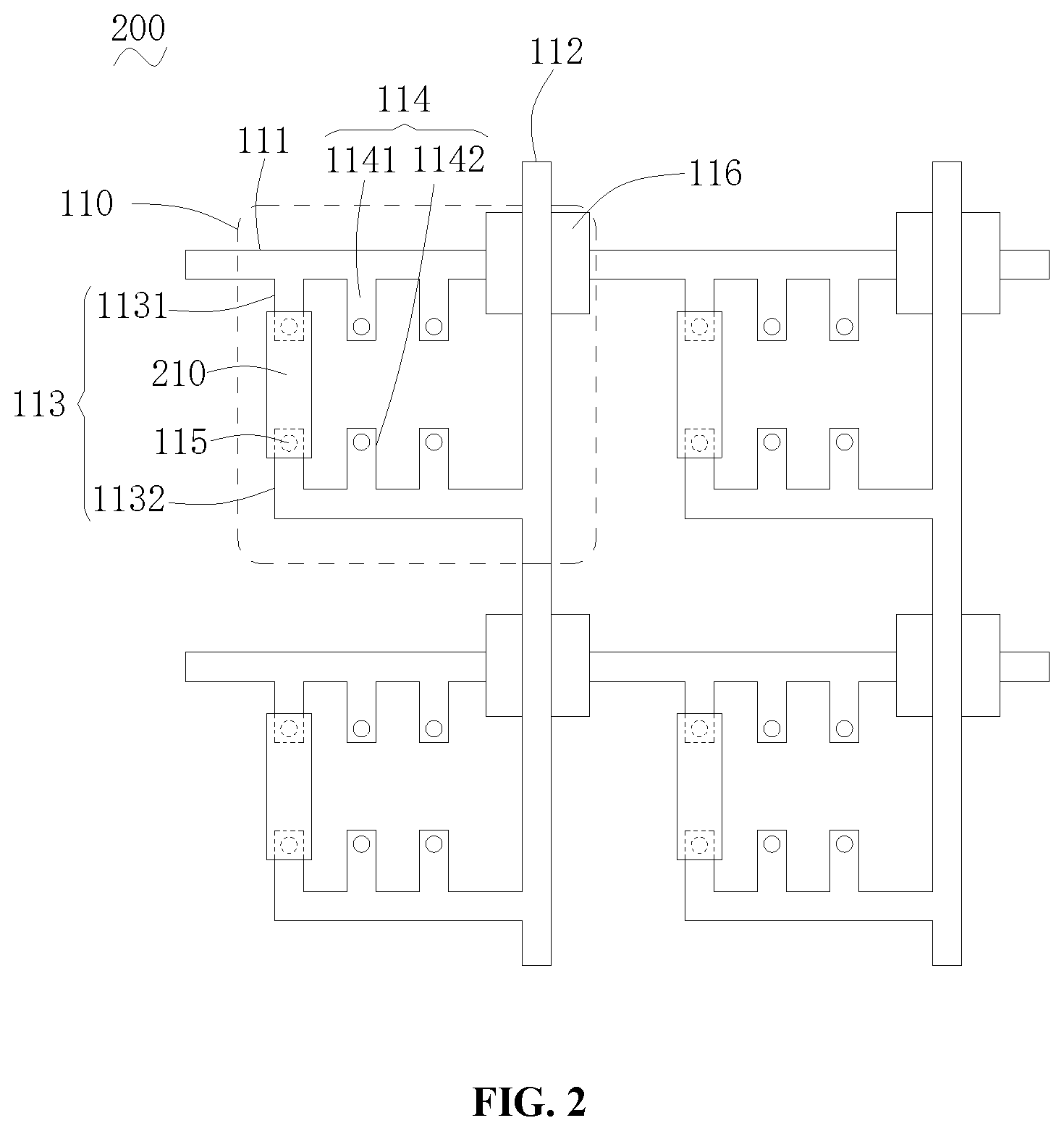
8. The driving backplane according to claim 7, wherein the driving backplane further comprises an insulating film located between the positions where the anode lead and the cathode lead are superposed.
9. The driving backplane according to claim 1, wherein the plurality of pixel units arranged in a same row share an anode lead.
10. The driving backplane according to claim 1, wherein the plurality of pixel units arranged in a same column share a cathode lead.
11. A micro-LED display panel comprises an LED chip and a driving backplane according to claim 1, wherein two ends of the LED chip are respectively soldered onto the anode and the cathode of any pair of electrodes of the at least two pairs of electrodes.
12. A micro-LED display device comprises a micro-LED display panel according to claim 11.
Description
CROSS-REFERENCES TO RELATED APPLICATIONS
[0001] The present application is a continuation of International Application No. PCT/CN2018/098604 filed on Aug. 3, 2018, which claims priority to Chinese patent application No. 201820440383.8, filed on Mar. 29, 2018. Both applications are incorporated herein by reference in their entireties.
TECHNICAL FIELD
[0002] The present disclosure relates to a display technology.
BACKGROUND
[0003] A micro light-emitting diode (micro-LED) display device implements image display by display pixels which is an array of microscopic LED of high density integrated on a substrate. Like a large-sized outdoor LED display, each pixel of the micro-LED display can be addressed and individually driven to illuminate, so it can be regarded as a micro-sized outdoor LED display screen with a pixel pitch reduced from millimeters to microns. The micro-LED display device, which is self-emissive, has advantages of better material stability, longer service life, no image imprint and the like when compared with an OLED display device, and has more application potential.
[0004] There are various challenges associated with micro-LED manufacturing processes. New and improved techniques are desired.
SUMMARY
[0005] Based on the above, it is necessary to provide a driving backplane that can improve the product yield of the micro-LED display panel, a micro-LED display panel, and a micro-LED display device in view of the problem of how to improve the product yield of the micro-LED display panel.
[0006] A driving backplane of a micro-LED display panel includes a plurality of pixel units arranged in an array, each of the pixel units including:an anode lead; a cathode lead disposed at a side of the anode lead; and at least two pairs of electrodes, each pair of electrodes of the at least two pairs of electrodes including an anode and a cathode disposed opposite to each other, a first anode of a first electrode pair being electrically connected to a second anode lead of a second electrode pair, and a first cathode of the first electrode air being electrically connected to a second cathode lead of the second electrode pair.
[0007] In the course of using the foregoing driving backplane, it is only necessary to solder an LED chip on one pair of electrodes of the at least two pairs of electrodes. In the case of a defective LED chip, a normal LED chip can be soldered on one pair of electrodes of a remaining pair of electrodes, so as to repair an LED pixel and improve product yield of display panels.
[0008] In an embodiment, each pair of electrodes of the at least two pairs of electrodes is spatially independent from an adjacent pair of electrodes.
[0009] In an embodiment, the at least two pairs of electrodes are at least three pairs of electrodes.
[0010] In an embodiment, the at least two pairs of electrodes are three pairs of electrodes sequentially spaced apart.
[0011] In an embodiment, the pixel unit further includes a plurality of chip pads disposed on the at least two pairs of electrodes.
[0012] In an embodiment, the chip pad is provided on both the anode and the cathode of each pair of electrodes of the at least two pairs of electrodes.
[0013] In an embodiment, the anode lead is arranged perpendicular to the cathode lead.
[0014] In an embodiment, the driving backplane further includes an insulating film located between the positions where the anode lead and the cathode lead are superposed.
[0015] In an embodiment, the plurality of pixel units arranged in a same row share an anode lead.
[0016] In an embodiment, the plurality of pixel units arranged in a same column share a cathode lead.
[0017] The present disclosure further provides a micro-LED display panel comprising an LED chip and the above driving backplane, wherein two ends of the LED chip are respectively soldered onto the anode and the cathode of any pair of electrodes of the at least two pairs of electrodes.
[0018] In the course of using a micro-LED display panel of the present disclosure, a normal LED chip can be soldered onto one pair of electrodes of a remaining pair of electrode in the case of a defective LED chip, so as to repair an LED pixel and improve the product yield of the display panel.
[0019] In addition, The present disclosure further provides a micro-LED display, which includes the micro-LED display panel described above.
[0020] Since the micro-LED display device disclosed herein includes the foregoing micro-LED display panel, in the course of use, a normal LED chip can be soldered onto one pair of electrodes of a remaining pair of electrodes in the case of a defective LED chip, so as to repair the LED pixel and improve the product yield of display panels, thereby improving the product yield of the micro-LED display device.
BRIEF DESCRIPTION OF THE DRAWINGS
[0021] FIG. 1 is a schematic diagram of a driving backplane of a micro-LED display panel according to an embodiment of the present disclosure.
[0022] FIG. 2 is a schematic diagram of a micro-LED display panel according to an embodiment of the present disclosure.
[0023] FIG. 3 is a schematic diagram of a micro-LED display panel using a backup pair of electrode according to an embodiment of the present disclosure.
DETAILED DESCRIPTION OF THE INVENTION
[0024] As mentioned above, there are various challenges associated with fabrication of micro-LED devices. In the preparation of the micro-LED display panel, LED chip arrays are transferred and soldered in batch onto a driving backplane. However, in the conventional processing of the micro-LED display panel, it is difficult to repair a defective LED pixel, resulting in a lower yield of display panels.
[0025] In order that the above objects, features and advantages of the present disclosure may be more clearly understood, specific embodiments of the present disclosure will be described in detail below with reference to the accompanying drawings. Numerous specific details are set forth in the following description in order to facilitate a thorough understanding of the present disclosure. The present disclosure can be embodied in many other ways than the description herein, and those skilled in the art can make similar modifications without departing from the spirit of the present disclosure, the disclosure is therefore not limited by the specific embodiments disclosed hereunder.
[0026] Referring to FIG. 1, a driving backplane 100 of a micro-LED display panel according to an embodiment includes a plurality of pixel units 110 arranged in an array. Each pixel unit 110 includes an anode lead 111, a cathode lead 112, and at least two pairs of electrodes.
[0027] The anode lead 111 and the cathode lead 112 are configured to transmit an electrical signal. The cathode lead 112 is located at a side of the anode lead 111.
[0028] Each pair of electrode includes an anode and a cathode disposed opposite to each other. The anode is electrically connected to the anode lead 111, and the cathode is electrically connected to the cathode lead 112. Each pair of electrode is spatially independent from an adjacent pair of electrodes, which can avoid damage to the adjacent pair of electrodes when an LED chip is soldered on pairs of electrodes.
[0029] For the purpose of explanation, in the present embodiment, a pair of electrodes subsequently soldered with LED chips is referred as the main pair of electrodes 113, and a pair of electrodes to be used subsequently as a backup is referred to as the backup pairs of electrodes 114. Definitely, the positions and the numbers of the main pair of electrodes 113 and the backup pair of electrodes 114 are not limited thereto.
[0030] The main pair of electrodes 113 includes a main anode 1131 and a main cathode 1132 disposed opposite to each other. The main anode 1131 is electrically connected to the anode lead 111, and the main cathode 1132 is electrically connected to the cathode lead 112.
[0031] The backup pair of electrodes 114 is configured to replace the main pair of electrodes 113. The backup pair of electrodes 114 includes a backup anode 1141 and a backup cathode 1142 disposed opposite to the backup anode 1141. The backup anode 1141 is electrically connected to the anode lead 111, and the backup cathode 1142 is electrically connected to the cathode lead 112.
[0032] Based on the foregoing embodiments, the at least two pairs of electrodes are at least three pairs of electrodes. As a result, more pairs of electrodes can be used as a backup, and a service life of the pixel unit 110 and the entire driving backplane 100 can be extended.
[0033] On the basis of the foregoing embodiments, the at least two pairs of electrodes are three pairs of electrodes arranged sequentially spaced apart. That is, there are two backup pairs of electrodes 114, and the main pair of electrodes 113 and the two backup pairs of electrodes 114 are sequentially spaced apart.
[0034] On the basis of the foregoing embodiments, the pixel unit 110 further includes a plurality of chip pads 115 on the at least two pairs of electrodes. The chip pad 115 is configured to solder the LED chip onto a pair of electrodes. As shown in FIG. 1, a chip pad 115 is provided on both the anode and cathode of each pair of electrodes.
[0035] Definitely, the LED chip may be soldered onto a pair of electrodes by other methods.
[0036] On the basis of the foregoing embodiment, the anode lead 111 is arranged perpendicular to the cathode lead 112, as shown in FIG. 1. Since the anode lead 111 and the cathode lead 112 are in perpendicular arrangement, a rectangular space is formed between the adjacent two anode leads 111 and the adjacent two cathode leads 112, which provides a more regular space for the arrangement of at least two pairs of electrodes of the pixel units 110, and facilitates orderly arrangement of the at least two pairs of electrodes. In addition, it further facilitates production and manufacture.
[0037] On the basis of the foregoing embodiment, the driving backplane 100 further includes an insulating film 116 located between the positions where the anode lead 111 and the cathode lead 112 are superimposed. The insulating film 116 prevents the anode lead 111 and the cathode lead 112 from being electrically connected.
[0038] On the basis of the foregoing embodiment, the plurality of pixel units 110 arranged in a same row share an anode lead 111. This arrangement processing may shorten the production time, thereby reducing the production cost.
[0039] On the basis of the foregoing embodiments, the plurality of pixel units 110 arranged in the same column share a cathode lead 112. This arrangement processing may shorten the production time, thereby reducing the production cost.
[0040] When the foregoing driving backplane is used, an LED chip may be soldered onto one pair of electrodes. If the LED chip is defective, a normal LED chip may be soldered onto one pair of electrodes of a remaining pair of electrodes, so that a LED pixel may be repaired and the product yield of display panels is improved.
[0041] Referring to FIG. 2, a micro-LED display panel 200 according to an embodiment includes an LED chip 210 and the above driving backplane 100. Both ends of the LED chip 210 are respectively soldered to the anode and the cathode of one pair of electrodes.
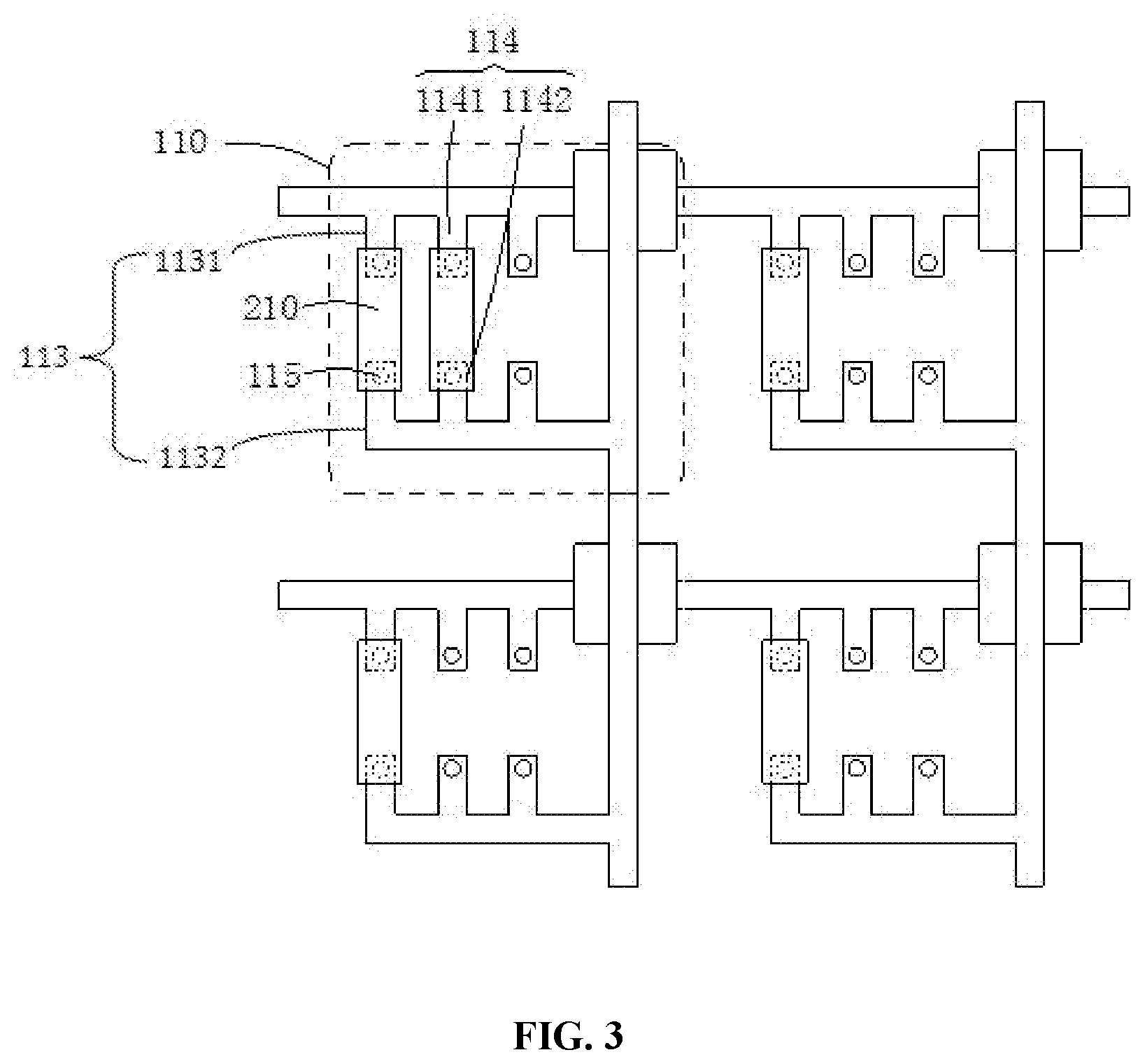
[0042] Referring to FIG. 3, taking a defective LED chip 210 for a left pixel unit 110 of the driving backplane 100 of the micro-LED display panel as an example, the micro-LED display panel 200 of the present disclosure is used under following principle:
[0043] when the LED chip 210 soldered to the main pair of electrodes 113 is defective, it is only necessary to solder a normal LED chip onto one backup pairs of electrodes of backup pairs of electrodes 114, so that the LED pixel may be repaired. Specifically, the normal LED chip 210 may be soldered to the chip pads 115 of the backup anode 1141 and the backup cathode 1142.
[0044] Definitely, if the LED chip 210 for the other pixel units 110 is defective, the described method may also be adopted. It is only necessary to solder a normal LED chip on one backup pair of electrodes of the backup pairs of electrodes 114, so that the LED pixel may be repaired. If the LED chip soldered to the backup pair of electrodes 114 is defective, the normal LED chip may be then soldered onto one pair of electrodes of remaining backup pairs of electrodes 114. The above operation is simple and easy.
[0045] In the micro-LED display panel 200 of the present disclosure, if the LED chip 210 is defective in use, a normal LED chip can be soldered on one pair of electrodes of a remaining pair of electrodes, so as to repair the LED pixel and improve the product yield of the display panel.
[0046] The micro-LED display device according to an embodiment includes the micro-LED display panel described above.
[0047] Since the micro-LED display device of the present disclosure includes the micro-LED display panel 200 described above, if the LED chip 210 is defective in use, a normal LED chip may be soldered onto one pair of electrodes of a remaining pair of electrodes, so as to repair the LED pixel and improve the product yield of the display panel, and thereby improving the product yield of micro-LED display devices.
[0048] Each of technical features of the above-described embodiments may be combined arbitrarily. To simplify the description, not all of possible combinations of each of the technical features in the above embodiments are described. However, all of the combinations of these technical features should be considered as within the scope of the present specification, as long as such combinations do not contradict with each other.
[0049] The above embodiments merely illustrate several embodiments of the present application, and the description thereof is specific and detailed, but it shall not be constructed as limiting the scope of the present application. It should be noted that, for a person of ordinary skill in the art, several variations and improvements may be made without departing from the concept of the present application, and these are all within the protection scope of the present application. Therefore, the protection scope of the present application shall be subject to the appended claims.
* * * * *
D00000
D00001
D00002
D00003
XML
uspto.report is an independent third-party trademark research tool that is not affiliated, endorsed, or sponsored by the United States Patent and Trademark Office (USPTO) or any other governmental organization. The information provided by uspto.report is based on publicly available data at the time of writing and is intended for informational purposes only.
While we strive to provide accurate and up-to-date information, we do not guarantee the accuracy, completeness, reliability, or suitability of the information displayed on this site. The use of this site is at your own risk. Any reliance you place on such information is therefore strictly at your own risk.
All official trademark data, including owner information, should be verified by visiting the official USPTO website at www.uspto.gov. This site is not intended to replace professional legal advice and should not be used as a substitute for consulting with a legal professional who is knowledgeable about trademark law.