Selective Deposition Method To Form Air Gaps
Zhu; Chiyu
U.S. patent application number 16/685787 was filed with the patent office on 2020-04-02 for selective deposition method to form air gaps. The applicant listed for this patent is ASM IP Holding B.V.. Invention is credited to Chiyu Zhu.
| Application Number | 20200105579 16/685787 |
| Document ID | / |
| Family ID | 1000004500396 |
| Filed Date | 2020-04-02 |


View All Diagrams
| United States Patent Application | 20200105579 |
| Kind Code | A1 |
| Zhu; Chiyu | April 2, 2020 |
SELECTIVE DEPOSITION METHOD TO FORM AIR GAPS
Abstract
A method for depositing a film to form an air gap within a semiconductor device is disclosed. An exemplary method comprises pulsing a metal halide precursor onto the substrate and pulsing an oxygen precursor onto a selective deposition surface. The method can be used to form an air gap to, for example, reduce a parasitic resistance of the semiconductor device.
| Inventors: | Zhu; Chiyu; (Helsinki, FI) | ||||||||||
| Applicant: |
|
||||||||||
|---|---|---|---|---|---|---|---|---|---|---|---|
| Family ID: | 1000004500396 | ||||||||||
| Appl. No.: | 16/685787 | ||||||||||
| Filed: | November 15, 2019 |
Related U.S. Patent Documents
| Application Number | Filing Date | Patent Number | ||
|---|---|---|---|---|
| 15836547 | Dec 8, 2017 | 10541173 | ||
| 16685787 | ||||
| 15205890 | Jul 8, 2016 | 9859151 | ||
| 15836547 | ||||
| Current U.S. Class: | 1/1 |
| Current CPC Class: | H01L 21/7682 20130101; H01L 21/02167 20130101; H01L 21/0228 20130101; H01L 21/02175 20130101; H01L 21/76832 20130101; H01L 21/02164 20130101; H01L 21/02271 20130101 |
| International Class: | H01L 21/768 20060101 H01L021/768; H01L 21/02 20060101 H01L021/02 |
Claims
1. A method of forming an air gap for a semiconductor device through selective deposition comprising: providing a substrate for processing in a reaction chamber; forming a first surface overlying the substrate for selectively depositing a film, wherein the first surface comprises a first substantially vertical portion; forming a second surface, wherein the second surface comprises a second substantially vertical portion; and selectively depositing the film at least on the first substantially vertical portion of the first surface relative to the second substantially vertical portion, wherein a portion of the film at least partially defines the air gap.
2. The method of claim 1, further comprising forming a third surface and forming a fourth surface, wherein the third surface comprises the same material as the first surface, wherein the fourth surface comprises the same material as the second surface, and wherein the deposition is selective on third surface relative to the deposition the fourth surface.
3. The method of claim 2, wherein both the third and the fourth surfaces comprise substantially vertical portions and selectively depositing the film comprises deposition on the said first and third vertical surfaces.
4. The method of claim 1, wherein the step of selectively depositing the film substantially closes the air gap.
5. The method of claim 1, further comprising: forming a dielectric layer at least on top of the film, wherein the dielectric layer defines a portion of the air gap.
6. The method of claim 5, wherein the step of forming the dielectric layer comprises a non-conformal deposition process.
7. The method of claim 1, wherein the step of selectively depositing the film is performed such that the film grows horizontally from the first substantially vertical portion toward the second substantially vertical portion.
8. The method of claim 1, wherein the step of selectively depositing the film comprises chemical vapor deposition.
9. The method of claim 1, wherein the thickness of the film is greater than 10 nm.
10. The method of claim 1, wherein the selectivity of deposition of the film on the first substantially vertical portion of the first surface relative to the second substantially vertical portion is greater than 80%.
11. The method of claim 1, wherein the air gap is part of integrated circuit and has a performance similar to dielectric material with k-value of less than 3.6.
12. The method of claim 1, wherein the air gap is part of an integrated circuit and size of the air gap is more than 35% of the space between metallization lines.
13. The method of claim 1, wherein the film comprises a low-k material.
14. The method of claim 1, wherein the film comprises an insulating material.
15. The method of claim 1, wherein the first surface comprises metal and the second surface comprises silicon.
16. The method of claim 1, wherein the step of selectively depositing the film comprises: pulsing a metal halide precursor on the first substantially vertical surface; pulsing an oxygen precursor on the first substantially vertical surface; and repeating the pulsing steps until the film grows to a desired thickness.
17. The method of claim 16, wherein the metal halide precursor comprises one or more of NbCl5 and TaCl5.
18. The method of claim 16, wherein the oxygen precursor comprises at least one of: water (H2O), oxygen (O2), ozone (O3), hydrogen peroxide (H2O2), atomic oxygen (O), oxygen radicals, and oxygen plasma.
19. The method of claim 16, wherein a temperature of the reaction chamber ranges between 20 and 600.degree. C.
20. The method of claim 1, wherein second surface comprises a liner.
Description
CROSS-REFERENCE TO RELATED APPLICATION
[0001] This application is a continuation of, and claims priority to and the benefit of, U.S. patent application Ser. No. 15/836,547, filed on Dec. 8, 2017 and entitled "SELECTIVE DEPOSITION METHOD TO FORM AIR GAPS," which is a continuation of, and claims priority to and the benefit of, U.S. patent application Ser. No. 15/205,890, now U.S. Pat. No. 9,859,151, filed on Jul. 8, 2016 and entitled "SELECTIVE FILM DEPOSITION METHOD TO FORM AIR GAPS," both of which are incorporated herein by reference.
FIELD OF INVENTION
[0002] The present disclosure generally relates to processes for manufacturing electronic devices. More particularly, the disclosure relates to selectively forming films through atomic layer deposition (ALD) or chemical vapor deposition (CVD). Specifically, the disclosure discloses methods to form ALD or CVD films that can be used to form an air gap.
BACKGROUND OF THE DISCLOSURE
[0003] Generally, deposition of films has taken place in a manner such that layers are grown from the bottom in an upward direction. For example, a film grown on a wafer is often grown in a direction vertical to the wafer's surface. Other films may be grown vertically on a microstructure surface. Some examples of features created in this manner include trench filling, step formation, or FinFET features, for example.
[0004] Air gaps are features with applicability in film deposition. U.S. Pat. No. 7,304,388 to Dubin et al. discloses air gaps that are created by first forming a sacrificial interlayer dielectric and decomposing it. The formation may involve an etching step, which may cause problems and decrease the performance of the device. The formation may also involve a deposition step for protecting liners, metal or metallic surfaces, thus decreasing the size of the air gap and the performance of the device. For example, International Publication No. WO 2013/101096 to Fischer discloses air gap formation with a hood layer. The air gap formation may also include an etching step. Air gaps may be used both in back end of line (BEOL) processing or front end of line processing. Two examples of applications for air gaps include air gaps in metallization, such as Cu metallization, or air gaps in NAND memories.
[0005] As a result, a method for selectively forming an air gap through ALD or CVD processes resulting in increased performance is desired.
SUMMARY OF THE DISCLOSURE
[0006] In accordance with at least one embodiment of the invention, a method of forming an air gap for a semiconductor device through selective deposition is disclosed. The method comprises: providing a substrate for processing in a reaction chamber; providing a first surface for selectively depositing a film, wherein at least a part of the first surface is substantially vertical; and selectively depositing a film through a deposition method on the first surface in at least a horizontal direction, the film not being deposited on a second surface, wherein the second surface differs from the first surface; wherein selectively depositing the film defines in part an air gap.
[0007] For purposes of summarizing the invention and the advantages achieved over the prior art, certain objects and advantages of the invention have been described herein above. Of course, it is to be understood that not necessarily all such objects or advantages may be achieved in accordance with any particular embodiment of the invention. Thus, for example, those skilled in the art will recognize that the invention may be embodied or carried out in a manner that achieves or optimizes one advantage or group of advantages as taught or suggested herein without necessarily achieving other objects or advantages as may be taught or suggested herein.
[0008] All of these embodiments are intended to be within the scope of the invention herein disclosed. These and other embodiments will become readily apparent to those skilled in the art from the following detailed description of certain embodiments having reference to the attached figures, the invention not being limited to any particular embodiment(s) disclosed.
BRIEF DESCRIPTION OF THE DRAWING FIGURES
[0009] These and other features, aspects, and advantages of the invention disclosed herein are described below with reference to the drawings of certain embodiments, which are intended to illustrate and not to limit the invention.
[0010] FIG. 1 is a perspective view of a semiconductor device in accordance with at least one embodiment of the invention.
[0011] FIGS. 2A and 2B are cross-sectional views of a semiconductor device in accordance with at least one embodiment of the invention.
[0012] FIGS. 3A, 3B, 3C and 3D are cross-sectional views of a semiconductor device in accordance with at least one embodiment of the invention.
[0013] FIGS. 4A, 4B, 4C and 4D are cross-sectional views in accordance with at least one embodiment of the invention.
[0014] FIG. 5 is a cross-sectional view in accordance with at least one embodiment of the invention.
[0015] It will be appreciated that elements in the figures are illustrated for simplicity and clarity and have not necessarily been drawn to scale. For example, the dimensions of some of the elements in the figures may be exaggerated relative to other elements to help improve understanding of illustrated embodiments of the present disclosure.
DETAILED DESCRIPTION OF EXEMPLARY EMBODIMENTS
[0016] Although certain embodiments and examples are disclosed below, it will be understood by those in the art that the invention extends beyond the specifically disclosed embodiments and/or uses of the invention and obvious modifications and equivalents thereof. Thus, it is intended that the scope of the invention disclosed should not be limited by the particular disclosed embodiments described below.
[0017] Selective deposition is desirable in order to grow particular features for a variety of applications. One particular feature, air gaps, has been used in 14 nm nodes, which currently is the smallest node size manufactured. Air gaps created in the 14 nm node may have, for example, a height of approximately 140 nm and a width of approximately 50 nm. This gap can be formed in a trench of approximately 180 nm in height, the trench herein meaning the space in between the metallization lines. The area of the air gap may be approximately 6,500 nm.sup.2, while the trench can have an area of 19,700 nm.sup.2. The volume of the air gap could be in the range of 1,625,000-32,500,000 nm.sup.3, while the trench could have a volume of 4,925,000-98,500,000 nm.sup.3. The air gap can be approximately 33% of the size of the trench.
[0018] Embodiments according to the invention can result in a larger air gap in that it can be a greater percentage of the trench, such as 50-60%, for example. The size of the air gap may be more than about 35%, more than about 45%, more than about 50%, more than about 60%, more than about 70%, or more than about 80% of the size of the trench or the space between the metallization lines.
[0019] One of ordinary skill in the art would understand that different sizes for the air gap may be possible. For example, the height of the air gap may range between about 10 to about 500 nm, between about 20 to about 300 nm, between about 30 to about 200 nm. Also, the width of the air gap may range between about 5 to about 250 nm, preferably between about 10 to about 200 nm, or more preferably between about 20 to about 100 nm. Also, the width of the air gap may be less than about 50 nm, less than about 30 nm, less than about 20 nm or in some instances less than to about 10 nm. The width can be considered to be measured to a direction of the smaller dimension between the features, for example, the width between metallization lines, the longest dimension of the metallization lines being cross-sectional to width (i.e., the smaller dimension).
[0020] From this, the cross-sectional area of the air gap may range between 50-125,000 nm.sup.2, preferably between about 100 to about 50,000 nm.sup.2, or more preferably between about 200 to about 20,000 nm.sup.2. The cross-sectional area of the air gap herein can be considered to be a cross-sectional area of the air gap between the features of device. The area can be considered to be measured to a direction of the smallest dimension between the features, for example, the area between metallization lines, the longest dimension of the metallization lines being cross-sectional to the area. Furthermore, the size of the air gap in relation to the trench size may range between about 30-80%. Also, the volume of the air gap could be in the range from about 2,500 to about 5,000,000,000 nm.sup.3, preferably from about 10,000 to about 500,000,000 nm.sup.3, or more preferably from about 50,000 to about 50,000,000 nm.sup.3.
[0021] FIG. 1 is schematic and simplified for the purpose of illustrating the exemplary dimensions. FIG. 1 illustrates a semiconductor device 10 in accordance with at least one embodiment of the invention. The semiconductor device 10 comprises a first metallization line 20 and a second metallization line 30. The first metallization line 20 and the second metallization line 30 may comprise a material, such as copper or other appropriate metal. A gap may exist between the first metallization line 20 and the second metallization line 30. The gap may have a length 40, a height 50, and a width 60. In some embodiments, the air gap may be formed inside the gap and it may have a length, a height, and a width smaller than the length 40, the height 50, and the width 60 illustrated in the FIG. 1. In some embodiments, the cross-sectional area of the air gap may be measured or calculated by using the height and the width, of which directions are the same than height 50 and width 60 of the air gap formed inside the gap. In some embodiments, the width 60 may be considered to be the smallest or smaller dimension between the features. In some embodiments, the height 50 may be considered to be the smallest or smaller dimension between the features.
[0022] Advantages gained from a larger air gap may include improved performance, and reducing the effective k-value of the material in between the lines. For example, the dielectric constant of low-k materials may be approximately 2.52, but the dielectric constant of air is 1. Reduction of the dielectric constant through replacement of the low-k material with air reduces the Resistive-capacitive (RC) delay. In addition, the replacement may result in increased processing speed, use of less current, and reduction of operating temperature and parasitic resistance. In some embodiments, the structure having air gap may have a performance similar to a material with a k-value of less than about 3.9, less than about 3.6, less than about 3.3, less than about 3, less than about 2.7, less than about 2.5, and in some instances, the k-value could be less than about 2.3 or even less than about 2.0 when the material would be considered to replace the air gap.
[0023] Figures presented herein are simplified and do not necessarily illustrate all layers, structures or features of the exemplary integrated circuits or structures that can form part on an integrated circuit.
[0024] FIG. 2A illustrates a semiconductor device 100 in accordance with at least one embodiment of the invention. The semiconductor device 100 may include a wafer 110, a first layer 120, a second layer 130, and a capping layer 140. The wafer 110 may comprise semiconductor material, such as silicon, silicon germanium or compound semiconductors such as III-V or II-VI materials. The first layer 120 may be a metal layer on top of the wafer 110, and may comprise metal or metallic materials, such as copper or insulating or dielectric material, such as silicon dioxide based materials or low-k materials. In some embodiments, the first layer 120 may comprise silicon and oxygen, for example, silicon dioxide. In some embodiments, the first layer 120 may not comprise metal. In some embodiments, the first layer 120 may comprise semi-metal material. Additional layers may exist between the first layer 120 and the substrate 110; for example, there may be multiple metallization layers or transistor layers or contact layers disposed between the first layer 120 and the substrate 110. The second layer 130 may be formed on the first layer 120, and may comprise materials comprising metal, such as aluminum nitride tungsten, tungsten oxide or other metallic, metal or insulating material. In some instances, the second layer 130 may be of a different material than the first layer 120. In some embodiments, the second layer 130 may comprise a metal or metallic surface. In some embodiments, the second layer 130 may not comprise a semi-metal. In some embodiments, the second layer 130 may comprise metal and oxygen, such as metal oxide.
[0025] The capping layer 140 may be formed on the second layer 130 and may comprise silicon-based material, such as silicon dioxide, silicon nitride or mixtures thereof. The capping layer 140 may cover portions of the second layer 130, leaving a particular portion of the second layer 130 exposed. The capping layer 140 may be made of the same material as the first layer 120. In some embodiments, the capping layer 140 may comprise silicon and oxygen, for example, silicon dioxide. In some embodiments, the capping layer 140 may not comprise metal. In some embodiments, the capping layer 140 may comprise a semi-metal. It is on the exposed portion (e.g., a surface or vertical portion 135) of the second layer 130 on which selective deposition may take place.
[0026] FIG. 2B illustrates the semiconductor device 100 in accordance with at least one embodiment of the invention. Upon an exposed portion of the second layer 130 (e.g., surface 135), a film 150 is deposited substantially horizontally along a direction 160 via deposition method, such as ALD, CVD (e.g., cyclic or sequential CVD), or any other suitable chemical and vapor phase based deposition method resulting in selective deposition. The film 150 deposited may comprise an insulating or dielectric material (for example, silicon oxide (SiO.sub.2)), metal oxide materials, transition metal oxides (for example, niobium oxide (Nb.sub.2O.sub.5)), or another low-k material.
[0027] For a film 150 formed of metal oxide, the following process may be used. First a surface (e.g., surface 135) to deposit the film 150 on may be provided. Second, a pulsing step of a metal precursor such as metal halide, may take place. An example of a metal halide may be a transition metal halide, such as niobium fluoride, niobium chloride, tantalum fluoride, tantalum chloride, molybdenum fluoride, molybdenum chloride, tungsten fluoride, tungsten fluoride, vanadium fluoride, vanadium chloride, chromium fluoride, or chromium chloride. In some embodiments, the metal halide may be NbCl.sub.5 or TaCl.sub.5. The pulsing step may have a temperature ranging between 20 and 600.degree. C., preferably between 100 and 500.degree. C., preferably between 150 and 400.degree. C., and preferably between 175 and 375.degree. C. The pulsing step may have a duration ranging between 0.01 and 120 seconds, preferably between 0.025 and 20 seconds, preferably between 0.05 and 10 seconds, and preferably between 0.1 and 5 seconds.
[0028] Third, a pulsing step of an oxygen source, such as water, may take place for example. Other oxygen sources may include oxygen (O.sub.2), ozone (O.sub.3), hydrogen peroxide (H.sub.2O.sub.2), atomic oxygen (O), oxygen radicals, or oxygen plasma, among others. The pulsing step may have a temperature ranging between 20 and 600.degree. C., preferably between 100 and 500.degree. C., preferably between 150 and 400.degree. C., and preferably between 175 and 375.degree. C. The pulsing step may have a duration ranging between 0.01 and 120 seconds, preferably between 0.025 and 20 seconds, preferably between 0.05 and 10 seconds, and preferably between 0.1 and 5 seconds.
[0029] After the pulsing steps, a purging step may take place to expunge any excess precursor. In addition, the pulsing steps may be repeated to form a film of a desired thickness.
[0030] FIG. 3A illustrates a semiconductor device 200 in accordance with at least one embodiment of the invention. The semiconductor device 200 includes a wafer 210 and a first column comprising a first layer 220 comprising a first surface 225, a second layer 230 comprising a second surface 235, and a capping layer 240 comprising a third surface 245. The semiconductor device 200 may also include a second column comprising a first layer 220' comprising a fourth surface 225', a second layer 230' comprising a fifth surface 235', and a capping layer 240' comprising a sixth surface 245'. Surfaces 225, 235, 245, 225', 235', and 245' can be vertical portions or comprise vertical portions. The wafer 210 may comprise silicon, silicon germanium, or another III-V material. The first layer 220 and the first layer 220' may be a metal layer on top of the wafer 210, and may comprise copper or tungsten, for example. Additional layers may exist between the first layers 220 and 220' and the substrate 210; for example, there may be multiple metallization layers disposed between the first layers 220 and 220' and the substrate 210. The second layer 230 and the second layer 230' may be formed on the first layer 220 and the first layer 220', and may comprise aluminum nitride, silicon nitride (SiN), or silicon carbon nitride (SiCN).
[0031] The capping layer 240 and the capping layer 240' may be formed on the second layer 230 and the second layer 230'. The capping layer 240 and the capping layer 240' may comprise silicon oxide, niobium oxide (Nb.sub.2O.sub.5), or another low-k material. The capping layer 240 and the capping layer 230' may cover portions of the second layer 230 and the second layer 230', leaving a particular portion exposed (e.g., surfaces 235, 235'). It is on the exposed portion (e.g., surface 235, 235') of the second layer 230 and the second layer 230' on which selective deposition may take place.
[0032] FIG. 3B illustrates the semiconductor device 200A, which includes structure 200, in accordance with at least one embodiment of the invention. Upon an exposed portion (e.g., surfaces 235, 235') of the second layer 230 and the second layer 230', a film 250 and a film 250' are deposited substantially horizontally via deposition method, such as ALD, CVD, or any other suitable deposition method resulting in selective deposition. The film 250 deposited may comprise silicon oxide (SiO.sub.2), niobium oxide (Nb.sub.2O.sub.5), or another low-k material. The steps to form the film 250, 250' may be similar to those described in relation to FIG. 2B.
[0033] FIG. 3C illustrates a semiconductor device 200B, formed from structure 200A, in accordance with at least one embodiment of the invention. As the substantially horizontal deposition takes place, a film 250 (merged with film 250') may be formed to bridge the first column with the second column. A shape of the film 250 may be narrower in the middle due to crystalline alignment or due to deposition process itself. For example, before closing of the gap 250, there may be only a narrow pathway from the air gap to outside environment, which may be difficult to purge in reasonable time before the next precursor pulse. Without being bound to any theory, it may cause some CVD reactions to take place on and around the narrow pathway and it may cause closing of the gap and affect the shape of the film 250. However, other shapes for the film 250 are possible, including spherical or semispherical.
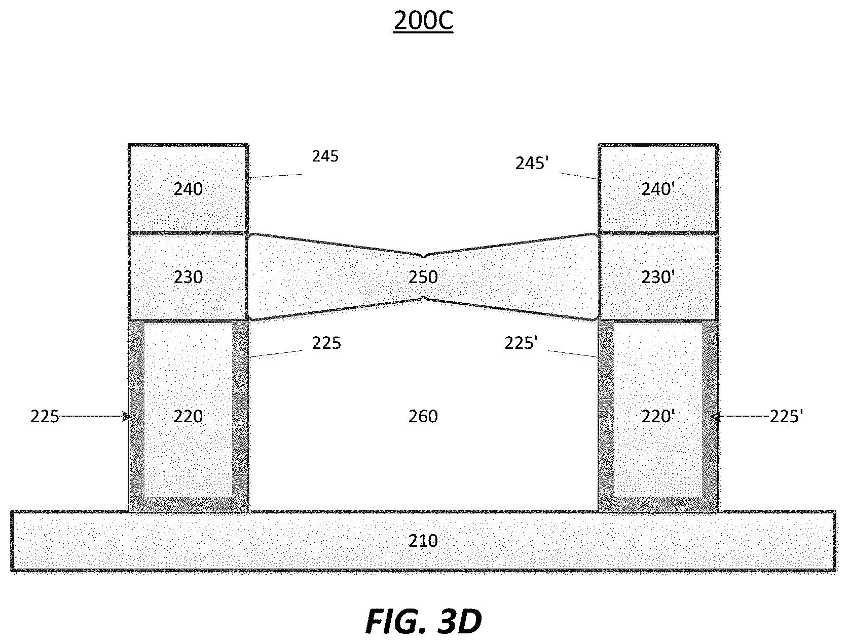
[0034] FIG. 3D illustrates a semiconductor device 200C in accordance with at least one embodiment of the invention. The first layer 220 may have a liner 225, while the first layer 220' may have a liner 225'. The liner 225 and the liner 225' may comprise titanium nitride (TiN), tantalum nitride (TaN), tungsten nitride (WN), tungsten (W), tantalum (Ta), titanium (Ti), or other appropriate metallic material. The liner 225 and the liner 225' may generally have the features of good conductivity, effective barrier properties, and good adhesion. Surfaces 225, 225' may comprise the liner material. As a result of the horizontal deposition, an air gap 260 may be formed. The air gap 260 serves as a replacement for a low-k dielectric material that would have been in its place.
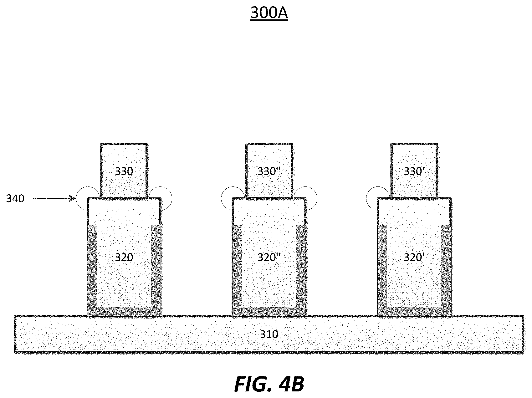
[0035] FIG. 4A illustrates a semiconductor device 300 in accordance with at least one embodiment of the invention. The semiconductor device 300 includes a wafer 310. The wafer 310 may comprise silicon, silicon germanium, or other III-V materials. Disposed on the wafer 310 are a plurality of first layers 320, 320', and 320''. The first layers 320, 320', and 320'' may comprise copper, tungsten, tantalum, or titanium, for example, and may be metallization lines in an integrated circuit. Covering a portion of the first layers 320, 320', and 320'' are a plurality of liners 325, 325', and 325''. The liners 325, 325', and 325'' may comprise titanium nitride (TiN), tantalum nitride (TaN), tungsten nitride (WN), tungsten (W), tantalum (Ta), titanium (Ti), or other appropriate metallic material.
[0036] A plurality of second layers 330, 330', and 330'' may be formed on the first layers 320, 320', and 330''. The second layers 330, 330', and 330'' may comprise aluminum nitride, silicon nitride (SiN), or silicon carbon nitride (SiCN), for example.
[0037] FIG. 4B illustrates the semiconductor device 300A in accordance with at least one embodiment of the invention. A portion (e.g., surfaces 335, 335', and 335', which can comprise vertical portions) of the first layers 320, 320', and 320'' is not covered by the liners 325, 325', and 325'' and the second layers 330, 330', and 330''. It is on this exposed portion of the first layers 320, 320' and 320'' that a plurality of films 340 may be formed. The plurality of films 340 may be formed through ALD, CVD, or any other suitable deposition method resulting in selective deposition.
[0038] The films 340 may comprise silicon oxide (SiO.sub.2), niobium oxide (Nb.sub.2O.sub.5), or another low-k material. The steps to form the film 340 may be similar to those described in relation to FIGS. 1B and 2B. The selective deposition takes place such that the film 340 forms on the exposed portions of the first layers 320, and 320', and 320''. The film 340 would not form on the liners 325, 325', and 325'' or the second layers 330, 330', and 330''.
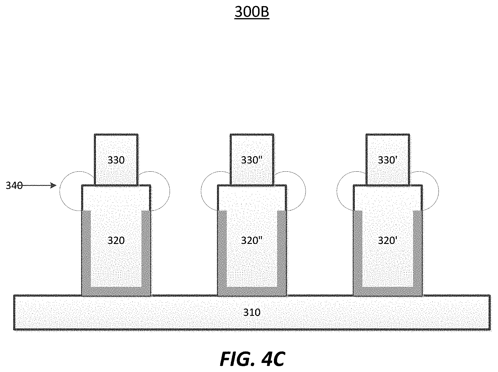
[0039] FIG. 4C illustrates the semiconductor device 300B in accordance with at least one embodiment of the invention. The films 340 may grow to a point that it covers all of the exposed portions of the first layers 320, 320', and 320''. The film 340 may first be grown in a conformal manner, but then grow in a non-conformal manner close to a surface of an opening of the trench or a space between the column stacks. The trench may be closed by the film 340 by a varying degree. For example, a percentage closure of the trench by the film 340 may be more than about 20%, more than about 40%, more than about 60%, or more than about 80%. Such may be also reflected by the amount of the film 340 deposited. For example, the film 340 may comprise more than about 1 nm of deposition, more than about 3 nm of deposition, more than about 5 nm of deposition, more than about 10 nm of deposition, or more than about 20 nm of deposition.
[0040] FIG. 4D illustrates the semiconductor device 300C in accordance with at least one embodiment of the invention. After the film 340 is formed, a first dielectric layer 350 and a second dielectric layer 350' may be formed through a CVD process with parameters resulting in a non-conformal film growth, such as non-conformal plasma enhanced chemical vapor deposition (PECVD) of a silicon oxide-based material, for example. The first dielectric layer 350 and the second dielectric layer 350' may comprise silicon based materials such as silicon dioxide (SiO.sub.2), silicon carbonitride (SiCN), or a low-k material, for example. The first dielectric layer 350 and the second dielectric layer 350' may be formed to create a first air gap 360 and a second air gap 360'. In addition, the dielectric layers 350 and 350' may be formed on the top of the second layers 330, 330', and 330''.
[0041] As shown in FIG. 4D, multiple air gaps may be formed between formed stacked layers. Gaps may be less than 200 nm, preferably less than 100 nm, more preferably less than 75 nm, and more preferably less than 50 nm. A smaller gap may be preferred as being better for ALD processing. In some embodiments, CVD processing may also be applied. By increasing the empty space of the air gaps, improved performance of the device may result.
[0042] As mentioned above, the selectivity may be expressed as the ratio of material formed on the first surface (A) minus the amount of material formed on the second surface (B) to amount of material formed on the first surface (A) (i.e., selectivity can be given as a percentage calculated by [(deposition on first surface)-(deposition on second surface)]/(deposition on the first surface) or [(A-B)/A]). Preferably, the selectivity may be above about 50%, above about 70%, above about 80%, above about 90%, above about 95%, above about 98%, above about 99% or about 100%. In some cases, selectivity above 80% may be acceptable for certain applications. In some cases, selectivity above 50% may be acceptable for certain applications. In some embodiments, the deposition temperature may be selected such that the selectivity is above about 95%. In some embodiments, the deposition temperature may be selected such that a selectivity of about 100% is achieved.
[0043] In some embodiments the thickness of the film that is selectively deposited is less than about 500 nm, less than about 250 nm, less than about 100 nm, less than about 50 nm or less than about 25 nm. In some embodiments, the thickness of the film that is selectively deposited may range from about 3 nm to about 200 nm or from about 5 nm to about 50 nm. However, in some cases a desired level of selectivity, for example more than 80%, or more than 90%, is achieved with the thicknesses of the selectively deposited film being over about 5 nm, over about 10 nm, over about 15 nm or over about 20 nm.
[0044] In some embodiments described above, one or more pretreatment and/or passivation processes or treatments of one or more of the surfaces of the substrate may be performed before selectively depositing the film. Passivation or pretreatments may enhance the selectivity and the growth on the desired surface and may decrease or block, in some instances almost completely block the growth on another surface. FIG. 5 illustrates such a structure in accordance with at least one embodiment of the invention. The structure may comprise a substrate 410, upon which a first column comprising a first layer 420 comprising a first surface comprising a first vertical portion 425 and a second layer 430 comprising a second surface comprising a second vertical portion 430 and a second column comprising a first layer 420' comprising a third surface comprising a third vertical portion and a second layer 430' comprising a fourth surface comprising a fourth vertical portion is formed. The first layer 420 and the first layer 420' may be subject to a pre-treatment or passivation step prior to the formation of a horizontal selective film 440. Once the formation of the horizontal selective film 440 is complete, an air gap 450 may be formed.
[0045] The particular implementations shown and described are illustrative of the invention and its best mode and are not intended to otherwise limit the scope of the aspects and implementations in any way. Indeed, for the sake of brevity, conventional manufacturing, connection, preparation, and other functional aspects of the system may not be described in detail. Furthermore, the connecting lines shown in the various figures are intended to represent exemplary functional relationships and/or physical couplings between the various elements. Many alternative or additional functional relationship or physical connections may be present in the practical system, and/or may be absent in some embodiments.
[0046] It is to be understood that the configurations and/or approaches described herein are exemplary in nature, and that these specific embodiments or examples are not to be considered in a limiting sense, because numerous variations are possible. The specific routines or methods described herein may represent one or more of any number of processing strategies. Thus, the various acts illustrated may be performed in the sequence illustrated, in other sequences, or omitted in some cases.
[0047] The subject matter of the present disclosure includes all novel and nonobvious combinations and subcombinations of the various processes, systems, and configurations, and other features, functions, acts, and/or properties disclosed herein, as well as any and all equivalents thereof.
* * * * *
D00000
D00001
D00002
D00003
D00004
D00005
D00006
D00007
D00008
D00009
D00010
D00011
D00012

XML
uspto.report is an independent third-party trademark research tool that is not affiliated, endorsed, or sponsored by the United States Patent and Trademark Office (USPTO) or any other governmental organization. The information provided by uspto.report is based on publicly available data at the time of writing and is intended for informational purposes only.
While we strive to provide accurate and up-to-date information, we do not guarantee the accuracy, completeness, reliability, or suitability of the information displayed on this site. The use of this site is at your own risk. Any reliance you place on such information is therefore strictly at your own risk.
All official trademark data, including owner information, should be verified by visiting the official USPTO website at www.uspto.gov. This site is not intended to replace professional legal advice and should not be used as a substitute for consulting with a legal professional who is knowledgeable about trademark law.