Fingerprint Sensing Module
Wang; Chung-Yi ; et al.
U.S. patent application number 16/531912 was filed with the patent office on 2020-04-02 for fingerprint sensing module. The applicant listed for this patent is Egis Technology Inc., Igistec Co., Ltd.. Invention is credited to Hsien-Hsiang Chiu, Yu-Hsuan Lin, Chung-Yi Wang.
| Application Number | 20200104561 16/531912 |
| Document ID | / |
| Family ID | 68142414 |
| Filed Date | 2020-04-02 |


| United States Patent Application | 20200104561 |
| Kind Code | A1 |
| Wang; Chung-Yi ; et al. | April 2, 2020 |
FINGERPRINT SENSING MODULE
Abstract
A fingerprint sensing module includes a fingerprint sensing pixel array with row output nodes or column output nodes, a current source, and control switches. The first terminals of the current source and the control switches are electrically coupled to the row output nodes or the column output nodes. The sensed content of each sensing pixel of the fingerprint sensing pixel array is outputted to the corresponding row output node or the corresponding column output node. Consequently, an output voltage is outputted. The second terminals of the current source and the control switches are electrically coupled to a first voltage and a second voltage, respectively. The voltage levels of the first voltage and the second voltage are different. When the control switches are turned on, the voltage level of the output voltage is equal to or close to the voltage level of the second voltage.
| Inventors: | Wang; Chung-Yi; (Hsinchu County, TW) ; Chiu; Hsien-Hsiang; (Hsinchu County, TW) ; Lin; Yu-Hsuan; (Hsinchu County, TW) | ||||||||||
| Applicant: |
|
||||||||||
|---|---|---|---|---|---|---|---|---|---|---|---|
| Family ID: | 68142414 | ||||||||||
| Appl. No.: | 16/531912 | ||||||||||
| Filed: | August 5, 2019 |
Related U.S. Patent Documents
| Application Number | Filing Date | Patent Number | ||
|---|---|---|---|---|
| 62740367 | Oct 2, 2018 | |||
| Current U.S. Class: | 1/1 |
| Current CPC Class: | G06K 9/0002 20130101; G06K 9/0004 20130101 |
| International Class: | G06K 9/00 20060101 G06K009/00 |
Foreign Application Data
| Date | Code | Application Number |
|---|---|---|
| Jun 25, 2019 | CN | 201910556231.3 |
Claims
1. A fingerprint sensing module, comprising: a fingerprint sensing pixel array comprising a plurality of sensing pixels, which are arranged in a plurality of columns and a plurality of rows, wherein the sensing pixels of each column are electrically coupled to a column output node, so that a plurality of column output nodes are electrically coupled to the plurality of sensing pixels of the fingerprint sensing pixel array, wherein in response to a control signal, sensed contents of the sensing pixels in each column are outputted to the column output node; a current source, wherein a first terminal of the current source is electrically coupled to the plurality of column output nodes, and a second terminal of the current source is electrically coupled to a first voltage; and a plurality of control switches, wherein a first terminal of each control switch is electrically coupled to the plurality of column output nodes, and a second terminal of each control switch is electrically coupled to a second voltage, wherein a voltage level of the second voltage is different from a voltage level of the first voltage, wherein after the sensed contents of the plurality of sensing pixels are outputted and the plurality of control switches are turned on in response to a reset signal, a voltage level of an output voltage at the column output node corresponding to the sensing pixels of each column is equal to or close to the voltage level of the second voltage.
2. The fingerprint sensing module as claimed in claim 1, wherein output terminals of at least two sensing pixels of each column are electrically coupled to the corresponding column output node.
3. The fingerprint sensing module as claimed in claim 1, wherein the voltage level of the first voltage is lower than the voltage level of the second voltage.
4. The fingerprint sensing module as claimed in claim 1, wherein the second voltage is provided by a voltage generation circuit.
5. The fingerprint sensing module as claimed in claim 4, wherein the voltage generation circuit is another current source, a biasing circuit or a buffer.
6. The fingerprint sensing module as claimed in claim 1, wherein when the plurality of control switches are turned on, a voltage difference between the first terminal and the second terminal of the current source is within a range between the voltage level of the first voltage and the voltage level of the second voltage, so that the current source is in a standby status.
7. The fingerprint sensing module as claimed in claim 1, wherein after the voltage level of the output voltage at the column output node is equal to or close to the voltage level of the second voltage, another sensing pixel of the column is subsequently sensed.
8. A fingerprint sensing module, comprising: a fingerprint sensing pixel array comprising a plurality of sensing pixels, which are arranged in a plurality of columns and a plurality of rows, wherein the sensing pixels of each row are electrically coupled to a row output node, so that a plurality of row output nodes are electrically coupled to the plurality of sensing pixels of the fingerprint sensing pixel array, wherein in response to a control signal, sensed contents of the sensing pixels in each row are outputted to the row output node; a current source, wherein a first terminal of the current source is electrically coupled to the plurality of row output nodes, and a second terminal of the current source is electrically coupled to a first voltage; and a plurality of control switches, wherein a first terminal of each control switch is electrically coupled to the plurality of row output nodes, and a second terminal of each control switch is electrically coupled to a second voltage, wherein a voltage level of the second voltage is different from a voltage level of the first voltage, wherein after the sensed contents of the plurality of sensing pixels are outputted and the plurality of control switches are turned on in response to a reset signal, a voltage level of an output voltage at the row output node corresponding to the sensing pixels of each row is equal to or close to the voltage level of the second voltage.
9. The fingerprint sensing module as claimed in claim 8, wherein output terminals of at least two sensing pixels of each row are electrically coupled to the corresponding row output node.
10. The fingerprint sensing module as claimed in claim 8, wherein the voltage level of the first voltage is lower than the voltage level of the second voltage.
11. The fingerprint sensing module as claimed in claim 8, wherein the second voltage is provided by a voltage generation circuit.
12. The fingerprint sensing module as claimed in claim 11, wherein the voltage generation circuit is another current source, a biasing circuit or a buffer.
13. The fingerprint sensing module as claimed in claim 8, wherein when the plurality of control switches are turned on, a voltage difference between the first terminal and the second terminal of the current source is within a range between the voltage level of the first voltage and the voltage level of the second voltage, so that the current source is in a standby status.
14. The fingerprint sensing module as claimed in claim 8, wherein after the voltage level of the output voltage from the row output node is equal to or close to the voltage level of the second voltage, another sensing pixel of the row is subsequently sensed.
Description
CROSS-REFERENCE TO RELATED APPLICATION
[0001] This application claims priority to U.S. Provisional Patent Application No. 62/740,367 filed Oct. 2, 2018 and Chinese Patent Application No. 201910556231.3 file Jun. 25, 2019, the contents of which are incorporated herein by reference.
FIELD OF THE INVENTION
[0002] The present invention relates to a fingerprint sensing module, and more particularly to a fingerprint sensing module capable of eliminating a memory effect.
BACKGROUND OF THE INVENTION
[0003] With the maturity of the modern fingerprint sensing technology, fingerprint sensing modules have been widely used in various electronic devices. For example, under-display fingerprint sensing modules have been applied to smart mobile devices such as digital cameras, scanners, smart phones, tablet computers or notebook computers.
[0004] FIG. 1A is a schematic circuit diagram illustrating a conventional fingerprint sensing module using a common current source. FIG. 1B is a waveform illustrating the voltage levels of the output voltage from some sensing pixels as shown in FIG. 1A. As shown in FIGS. 1A and 1B, the conventional fingerprint sensing module 10 includes a fingerprint sensing pixel array 110 and a current source 120. The fingerprint sensing pixel array 110 includes a plurality of sensing pixels, which are arranged in a plurality of columns and a plurality of rows. For succinctness, only one pixel row P.sub.1 of the fingerprint sensing pixel array 110 will be described as follows. The pixel row P.sub.1 includes a plurality of sensing pixels P.sub.11.about.P.sub.1n, which are electrically coupled to each other. The output terminals N.sub.11.about.N.sub.1n of the plurality of sensing pixels P.sub.11.about.P.sub.1n are electrically coupled to each other and electrically coupled to a row output node N.sub.1. The row output node N.sub.1 outputs an output voltage V.sub.1out. A first terminal of the current source 120 is electrically coupled to the row output node N.sub.1. A second terminal of the current source 120 is electrically coupled to a voltage VN.sub.1.
[0005] When the pixel row P.sub.1 receives a control signal C.sub.1, the plurality of sensing pixels P.sub.11.about.P.sub.1n are sequentially driven to output the sensed contents. In the time interval between 0 and t.sub.11, the sensed content of the sensing pixel P.sub.11 is outputted to the row output node N.sub.1 according to the control signal C.sub.11. Consequently, the output voltage V.sub.1out with a first voltage level V.sub.11 is outputted from the row output node N.sub.1. In the time interval between t.sub.11 and t.sub.12, the sensed content of the sensing pixel P.sub.12 is outputted to the row output node N.sub.1 according to the control signal C.sub.12. Consequently, the output voltage V.sub.1out with a second voltage level V.sub.12 is outputted from the row output node N.sub.1. In the time interval between t.sub.12 and t.sub.13, the sensed content of the sensing pixel P.sub.13 is outputted to the row output node N.sub.1 according to the control signal C.sub.13. Consequently, the output voltage V.sub.1out with a third voltage level V.sub.13 is outputted from the row output node N.sub.1.
[0006] Due to the parasitic effect of the practical circuitry wiring structure, a memory effect is generated when the output voltage V.sub.1out from the sensing pixels P.sub.11.about.P.sub.1n is sequentially read at different time points. For example, when one of the sensing pixels P.sub.11.about.P.sub.1n is driven and the corresponding sensed content is read, the output voltage V.sub.1out corresponding to the previous sensing pixel is still retained at the row output node N.sub.1. Because of the memory effect, the sensed contents of the sensing pixels P.sub.11.about.P.sub.1n to be outputted to the row output node N.sub.1 are adversely affected.
[0007] As mentioned above, the results of reading the sensed data of the fingerprint sensing pixel array 110 are adversely affected by the memory effect. For solving this drawback, a fingerprint sensing module as shown in FIG. 2A was provided.
[0008] FIG. 2A is a schematic circuit diagram illustrating a conventional fingerprint sensing module for overcoming the memory effect. FIG. 2B is a waveform illustrating the voltage levels of the output voltage from some sensing pixels as shown in FIG. 2A. As shown in FIGS. 2A and 2B, the conventional fingerprint sensing module 20 includes a fingerprint sensing pixel array 210, a current source 220 and a control switch 230. For succinctness, only the connection between one pixel row P.sub.2 of the fingerprint sensing pixel array 210 and associated components will be described as follows. The pixel row P.sub.2 includes a plurality of sensing pixels P.sub.21.about.P.sub.2n. The output terminals N.sub.21.about.N.sub.2n corresponding to the plurality of sensing pixels P.sub.21.about.P.sub.2n are electrically coupled to a row output node N.sub.2. The row output node N.sub.2 outputs an output voltage V.sub.2out. The row output node N.sub.2 is electrically coupled to a first terminal of the current source 220 and a first terminal of the control switch 230. A second terminal of the current source 220 is electrically coupled to a first voltage VN.sub.21. A second terminal of the control switch 230 is electrically coupled to a second voltage VN.sub.22. The voltage level of the first voltage VN.sub.21 and the voltage level of the second voltage VN.sub.22 are equal (e.g., equal to 0V).
[0009] When the pixel row P.sub.2 receives a control signal C.sub.2, the plurality of sensing pixels P.sub.21.about.P.sub.2n are sequentially driven to output the sensed contents. In the time interval between 0 and t.sub.21, the sensed content of the sensing pixel P.sub.21 is outputted to the row output node N.sub.2 according to the control signal C.sub.21. Consequently, the output voltage V.sub.2out with a first voltage level V.sub.21 is outputted from the row output node N.sub.2. Then, the control switch 230 is turned on in response to a reset signal Rst2. Consequently, the voltage level V.sub.21 of the output voltage V.sub.2out is equal to the voltage level of the first voltage VN.sub.21 and the voltage level of the second voltage VN.sub.22. That is, the voltage level V.sub.21 of the output voltage V.sub.2out is pulled down to 0V. Consequently, the residual memory effect caused by the sensing pixel P.sub.21 is eliminated.
[0010] In the time interval between t.sub.21 and t.sub.22, the sensed content of the sensing pixel P.sub.22 is outputted to the row output node N.sub.2 according to the control signal C.sub.22. Consequently, the output voltage V.sub.2out with a second voltage level V.sub.22 is outputted from the row output node N.sub.2. Then, the control switch 230 is turned on again in response to the reset signal Rst2. Consequently, the voltage level V.sub.22 of the output voltage V.sub.2out is pulled down to 0V. Consequently, the residual memory effect caused by the sensing pixel P.sub.22 is eliminated. The rest may be deduced by analog, and the voltage levels of the output voltage V.sub.2out from the pixel row P.sub.2 can be acquired.
[0011] As mentioned above, the voltage level of the first voltage VN.sub.21 is assumed to be equal to the voltage level of the second voltage VN.sub.22. When the control switch 230 is turned on to eliminate the memory effect, the voltage levels at the two terminals of the current source 220 are pulled to the same voltage level. Since there is no voltage difference between the two terminals of the current source 220, the driving capability of the current source 220 is lost and the current source 220 is disabled.
[0012] During the switching periods t.sub.21 to t.sub.2n, the terminal of the current source 220 electrically coupled to the row output node N.sub.2 has to slowly pull up the voltage level of the row output node N.sub.2 through the pixel row P.sub.2. Since the voltage level of the row output node N.sub.2 is increased, a voltage difference exists between the two terminals of the current source 220. Consequently, the current source 220 is enabled again until the voltage level at the row output node N.sub.2 is high enough to result in the normal operation of the current source 220. That is, it is necessary to increase the voltage level of the row output node N.sub.2 in advance in order to get better output of the current source 220. Consequently, the time interval between t.sub.21 and t.sub.2n contains the time period of increasing the voltage level of the row output node N.sub.2 to the operating voltage level of the current source 230 and the waiting time period of pulling down the voltage level of the output voltage V.sub.2out to 0V. In other words, the signal switching speed cannot be too fast. In practice, the voltage level of the row output node N.sub.2 ranges from 0V to the voltage level of the output voltage V.sub.2out. Consequently, it is necessary to pull down the voltage level of the row output node N.sub.2 to 0V to eliminate the residual memory effect of the sensing pixels P.sub.21.about.P.sub.2n. Moreover, after the voltage level reaches the operating voltage level of the current source 220, the sensed contents of the sensing pixels can be normally read. Consequently, the switching time intervals t.sub.21-t.sub.2n of reading the sensed contents of the sensing pixels P.sub.21.about.P.sub.2n are very long.
[0013] Therefore, there is a need of providing a novel fingerprint sensing module for effectively shortening the switching time period of reading pixels and eliminating the memory effect of the previous sensing pixel so as to overcome the drawbacks of the conventional technologies.
SUMMARY OF THE INVENTION
[0014] For overcoming the drawbacks of the conventional technologies, the present invention provides a fingerprint sensing module with a control switch. When the control switch is turned on in response to a reset signal, the voltage level of an output voltage from a row output node (or a column output node) is equal to or close to a voltage level of a second voltage.
[0015] In accordance with an aspect of the present invention, a fingerprint sensing module is provided. The fingerprint sensing module includes a fingerprint sensing pixel array, a current source and a plurality of control switches. The fingerprint sensing pixel array includes a plurality of sensing pixels, which are arranged in a plurality of columns and a plurality of rows. The sensing pixels of each column are electrically coupled to a column output node, so that a plurality of column output nodes are electrically coupled to the plurality of sensing pixels of the fingerprint sensing pixel array. In response to a control signal, sensed contents of the sensing pixels in each column are outputted to the column output node. A first terminal of the current source is electrically coupled to the plurality of column output nodes. A second terminal of the current source is electrically coupled to a first voltage. A first terminal of each control switch is electrically coupled to the plurality of column output nodes. A second terminal of each control switch is electrically coupled to a second voltage. A voltage level of the second voltage is different from a voltage level of the first voltage. After the sensed contents of the plurality of sensing pixels are outputted and the plurality of control switches are turned on in response to a reset signal, a voltage level of an output voltage at the column output node corresponding to the sensing pixels of each column is equal to or close to the voltage level of the second voltage.
[0016] In accordance with another aspect of the present invention, a fingerprint sensing module is provided. The fingerprint sensing module includes a fingerprint sensing pixel array, a current source and a plurality of control switches. The fingerprint sensing pixel array includes a plurality of sensing pixels, which are arranged in a plurality of rows and a plurality of rows. The sensing pixels of each row are electrically coupled to a row output node, so that a plurality of row output nodes are electrically coupled to the plurality of sensing pixels of the fingerprint sensing pixel array. In response to a control signal, sensed contents of the sensing pixels in each row are outputted to the row output node. A first terminal of the current source is electrically coupled to the plurality of row output nodes. A second terminal of the current source is electrically coupled to a first voltage. A first terminal of each control switch is electrically coupled to the plurality of row output nodes. A second terminal of each control switch is electrically coupled to a second voltage. A voltage level of the second voltage is different from a voltage level of the first voltage. After the sensed contents of the plurality of sensing pixels are outputted and the plurality of control switches are turned on in response to a reset signal, a voltage level of an output voltage at the row output node corresponding to the sensing pixels of each row is equal to or close to the voltage level of the second voltage.
[0017] From the above descriptions, the fingerprint sensing module of the present invention is additionally equipped with a control switch. After the control switch is turned on in response to the reset signal, the voltage level of the output voltage from the fingerprint sensing pixel array is pulled down to the voltage level of the second voltage. Consequently, the memory effect of each sensing pixel can be eliminated. Moreover, the voltage level of two terminals of the current source is within the range from the voltage level of the first voltage to the voltage level of the second voltage. Due to the difference between the voltage levels of the first voltage and the second voltage, the current source is in a standby state. When the current source in a standby state, the current source can enter the normal working state at any time. Consequently, the switching time period of reading the sensed content of each sensing pixel of the fingerprint sensing pixel array is shortened.
BRIEF DESCRIPTION OF THE DRAWINGS
[0018] The above objects and advantages of the present invention will become more readily apparent to those ordinarily skilled in the art after reviewing the following detailed description and accompanying drawings, in which:
[0019] FIG. 1A is a schematic circuit diagram illustrating a conventional fingerprint sensing module using a common current source;
[0020] FIG. 1B is a waveform illustrating the voltage levels of the output voltage from some sensing pixels as shown in FIG. 1A;
[0021] FIG. 2A is a schematic circuit diagram illustrating a conventional fingerprint sensing module for overcoming the memory effect;
[0022] FIG. 2B is a waveform illustrating the voltage levels of the output voltage from some sensing pixels as shown in FIG. 2A;
[0023] FIG. 3A is a schematic circuit diagram illustrating a fingerprint sensing module according to an embodiment of the present invention; and
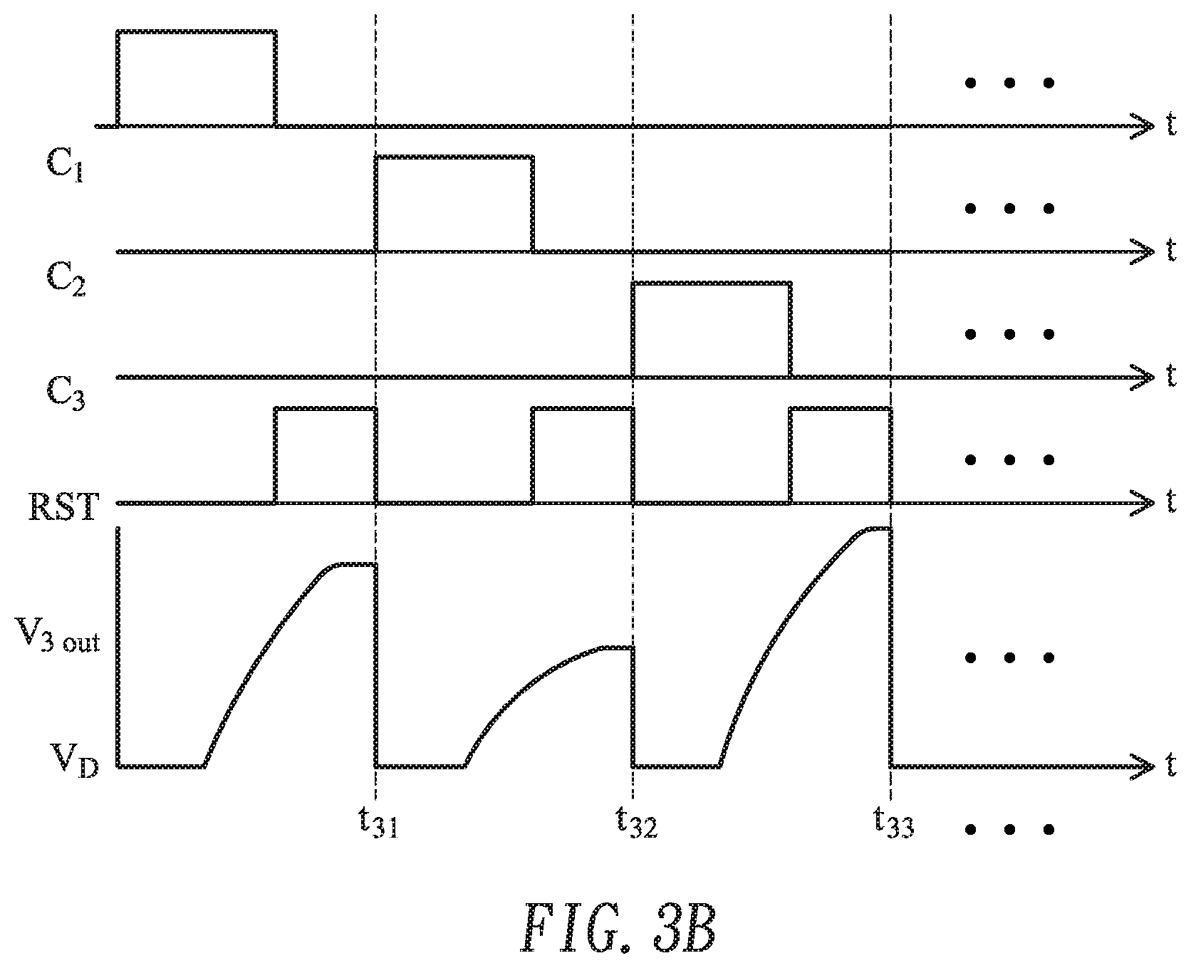
[0024] FIG. 3B is a waveform illustrating the voltage levels of the output voltage from some sensing pixels as shown in FIG. 3A.
DETAILED DESCRIPTION OF THE PREFERRED EMBODIMENT
[0025] The embodiments of present invention will be described more specifically with reference to the following drawings. In the following embodiments and drawings, the elements irrelevant to the concepts of the present invention or the elements well known to those skilled in the art are omitted. It is noted that numerous modifications and alterations may be made while retaining the teachings of the invention.
[0026] For overcoming the drawbacks of the conventional technologies, the present invention provides a novel fingerprint sensing module. FIG. 3A is a schematic circuit diagram illustrating a fingerprint sensing module according to an embodiment of the present invention. FIG. 3B is a waveform diagram illustrating the voltage levels of the output voltage from some sensing pixels as shown in FIG. 3A.
[0027] As shown in FIGS. 3A and 3B, the fingerprint sensing module 30 includes a fingerprint sensing pixel array 310, a current source 320 and a control switch 330. For succinctness, only the connection between a pixel row P.sub.3 of the fingerprint sensing pixel array 310 and associated components will be described as follows. The pixel row P3 includes a plurality of sensing pixels P.sub.31.about.P.sub.3n. The output terminals N.sub.31.about.N.sub.3n corresponding the plurality of sensing pixels P.sub.31.about.P.sub.3n are electrically coupled to each other and electrically coupled to a row output node N.sub.3. The row output node N.sub.3 outputs an output voltage V.sub.3out. The row output node N.sub.3 is electrically coupled to a first terminal of the current source 320 and a first terminal of the control switch 330. A second terminal of the current source 320 is electrically coupled to a first voltage VN.sub.31. A second terminal of the control switch 330 is electrically coupled to a second voltage VN.sub.32.
[0028] In an embodiment, the voltage level of the first voltage VN.sub.31 and the voltage level of the second voltage VN.sub.32 are different. For example, the voltage level of the second voltage VN.sub.32 is higher than the voltage level of the first voltage VN.sub.31. The second voltage VN.sub.32 is provided by a voltage generation circuit. For example, the voltage generation circuit is another current source, a biasing circuit or a buffer. In this embodiment, the voltage level of the second voltage VN.sub.32 is equal to V.sub.D. For example, the voltage level of V.sub.D is 3V or 3.3V.
[0029] When the pixel row P.sub.3 receives a control signal C3, the plurality of sensing pixels P.sub.31.about.P.sub.3 are sequentially driven to output the sensed contents. In the time interval between 0 and t.sub.31, the sensed content of the sensing pixel P.sub.31 is outputted to the row output node N.sub.3 according to the control signal C.sub.31. Consequently, the output voltage V.sub.3out with a first voltage level V.sub.31 is outputted from the row output node N.sub.3. Then, the control switch 330 is turned on in response to a reset signal Rst3. Consequently, the first voltage level V.sub.31 of the output voltage V.sub.3out from the row output node N.sub.3 is equal to the voltage level of the second voltage VN.sub.32. That is, the first voltage level V.sub.31 of the output voltage V.sub.3out is pulled down to V.sub.D. Since there is no voltage difference between the first voltage level V.sub.31 of the output voltage V.sub.3out and the voltage level of the second voltage VN.sub.32, the residual memory effect caused by the sensing pixel P.sub.31 is eliminated.
[0030] In the time interval between t.sub.31 and t.sub.32, the sensed content of the sensing pixel P.sub.32 is outputted to the row output node N.sub.3 according to the control signal C.sub.32. Consequently, the output voltage V.sub.3out with a second voltage level V.sub.32 is outputted from the row output node N.sub.3. Then, the control switch 330 is turned on in response to the reset signal Rst3. Consequently, the second voltage level V.sub.32 of the output voltage V.sub.3out from the row output node N.sub.3 is pulled down to V.sub.D, and the residual memory effect caused by the sensing pixel P.sub.32 is eliminated.
[0031] In the time interval between t.sub.32 and t.sub.33, the sensed content of the sensing pixel P.sub.33 is outputted to the row output node N.sub.3 according to the control signal C.sub.33. Consequently, the output voltage V.sub.3out with a third output voltage level V.sub.33 is outputted from the row output node N.sub.3. Then, the control switch 330 is turned on in response to the reset signal Rst3. Consequently, the third voltage level VN.sub.33 of the output voltage V.sub.3out from the row output node N.sub.3 is pulled down to V.sub.D, and the residual memory effect caused by the sensing pixel P.sub.33 is eliminated.
[0032] The rest may be deduced by analog. In such way, the voltage levels of the output voltage V.sub.3out from the pixel row P.sub.3 can be acquired sequentially.
[0033] From the above descriptions, the process of reading the pixel row P.sub.3 according to the present invention is beneficial. After the sensed content of the sensing pixel P.sub.31 is read and the output voltage V.sub.3out with the first voltage level V.sub.31 is outputted to the row output node N.sub.3, the first output voltage level V.sub.31 is pulled down to V.sub.D. Consequently, in the subsequent step, the sensed content of the sensing pixel P.sub.32 can be quickly read and the output voltage V.sub.3out with the second voltage level V.sub.32 can be outputted to the row output node N.sub.3. In other words, the long waiting time period of pulling down the voltage level of the output voltage V.sub.3out to the voltage level of the first voltage VN.sub.31 (e.g., a ground voltage level) is not required. Moreover, it is not necessary to increase the voltage level of the output voltage level V.sub.3out again to enable the current source 320. When the desired voltage difference between the two terminals of the current source 320 is achieved, the subsequent steps of reading the sensing contents of the sensing pixels of the pixel row P.sub.3 can be performed. In such way, the time interval between t.sub.31 and t.sub.3n for decreasing the difference between the voltage level of the output voltage level V.sub.3out and the voltage level of the second voltage VN.sub.32 is shortened. Consequently, the switching time intervals t.sub.31.about.t.sub.31, of the sensing pixels P.sub.31.about.P.sub.31, in the pixel row P.sub.3 are obviously shorter than the switch time intervals t.sub.21-t.sub.2n of the sensing pixels P.sub.21.about.P.sub.2n in the conventional fingernail sensing module.
[0034] Moreover, when the control switch 330 is turned on, the voltage levels at the two terminals of the current source 320 are within the range from the voltage level of the first voltage VN.sub.31 to the voltage level of the second voltage VN.sub.32. Since the current source 320 has the voltage difference between the voltage level of the first voltage VN.sub.31 and the voltage level of the second voltage VN.sub.32, the current source 320 is in a standby state. When the current source 320 is in a standby state, the current source 320 can enter the normal working state at any time. That is, the current source 320 can be enabled again without the need of receiving the voltage level from the row output node N.sub.3.
[0035] It is noted that numerous modifications and alterations may be made while retaining the teachings of the invention. That is, the structural designs and specifications of the components may be varied according to the practical requirements. For example, the control switch is a transistor. According to the initial voltage value of the fingerprint sensing pixel array, the voltage level of the second voltage is dynamically adjusted to the proper voltage level V.sub.D. For example, the voltage level of the second voltage is specially set. Consequently, the voltage level of the terminal receiving the reset signal Rst minus the voltage level V.sub.D of the second voltage is certainty higher than the gate startup voltage V.sub.th.
[0036] As mentioned above, the fingerprint sensing pixel array includes a plurality sensing pixels, which are arranged in a plurality of columns and a plurality of rows. In an embodiment, the output terminals of the plurality of sensing pixels in any column are electrically coupled to a column output node. Alternatively, in another embodiment, the output terminals of the plurality of sensing pixels in any row are electrically coupled to a row output node.
[0037] In the above embodiment, the current source and the control switch are electrically coupled to any row output signal. In accordance with the spirits of the present invention, the first terminal of the current source and the first terminal of the control switch are electrically coupled to the first voltage and the second voltage, respectively. After the control switch is turned on in response to the reset signal, the voltage level of the output voltage of the fingerprint sensing pixel array is pulled down to the voltage level of the second voltage. Consequently, the memory effect of each sensing pixel can be eliminated. Alternatively, the current source and the control switch are electrically coupled to any column output signal. Similarly, the purpose of eliminating the memory effect can be achieved.
[0038] From the above descriptions, the fingerprint sensing module of the present invention is additionally equipped with a control switch. After the control switch is turned on in response to the reset signal, the voltage level of the output voltage from the fingerprint sensing pixel array is pulled down to the voltage level of the second voltage. Consequently, the memory effect of each sensing pixel can be eliminated. Moreover, the voltage level of the two terminals of the current source is within the range from the voltage level of the first voltage to the voltage level of the second voltage. Due to the difference between the voltage levels of the first voltage and the second voltage, the current source is in a standby state. When the current source in a standby state, the current source can enter the normal working state at any time. Consequently, the switching time period of reading the sensed content of each sensing pixel of the fingerprint sensing pixel array is shortened.
[0039] While the invention has been described in terms of what is presently considered to be the most practical and preferred embodiments, it is to be understood that the invention needs not be limited to the disclosed embodiments. On the contrary, it is intended to cover various modifications and similar arrangements included within the spirit and scope of the appended claims which are to be accorded with the broadest interpretation so as to encompass all modifications and similar structures.
* * * * *
D00000
D00001
D00002
D00003
D00004
XML
uspto.report is an independent third-party trademark research tool that is not affiliated, endorsed, or sponsored by the United States Patent and Trademark Office (USPTO) or any other governmental organization. The information provided by uspto.report is based on publicly available data at the time of writing and is intended for informational purposes only.
While we strive to provide accurate and up-to-date information, we do not guarantee the accuracy, completeness, reliability, or suitability of the information displayed on this site. The use of this site is at your own risk. Any reliance you place on such information is therefore strictly at your own risk.
All official trademark data, including owner information, should be verified by visiting the official USPTO website at www.uspto.gov. This site is not intended to replace professional legal advice and should not be used as a substitute for consulting with a legal professional who is knowledgeable about trademark law.