Optical Image Capturing Module
CHANG; YEONG-MING ; et al.
U.S. patent application number 16/227652 was filed with the patent office on 2020-03-26 for optical image capturing module. The applicant listed for this patent is ABILITY OPTO-ELECTRONICS TECHNOLOGY CO., LTD.. Invention is credited to YEONG-MING CHANG, CHIEN-HSUN LAI, YAO-WEI LIU.
| Application Number | 20200096736 16/227652 |
| Document ID | / |
| Family ID | 69885453 |
| Filed Date | 2020-03-26 |


View All Diagrams
| United States Patent Application | 20200096736 |
| Kind Code | A1 |
| CHANG; YEONG-MING ; et al. | March 26, 2020 |
OPTICAL IMAGE CAPTURING MODULE
Abstract
An optical image capturing module includes a lens assembly and a circuit assembly including a circuit substrate having a through hole and an image sensing component. A lower surface of the circuit substrate has multiple circuit contacts. A sensing surface of the image sensing component has multiple image contacts. Each image contact is electrically connected to one of the circuit contacts via a signal transmission element, thereby the sensing surface directly faces the through hole. The lens assembly includes a fixed base disposed on an upper surface of the circuit substrate, a movable base disposed in a focusing hole, and a lens group disposed in the movable base. The fixed base has the focusing hole penetrating through two ends thereof. The lens group includes at least two lenses having refractive power, thereby light could pass through the lens group and the through hole and project onto the image sensing component.
| Inventors: | CHANG; YEONG-MING; (TAICHUNG CITY, TW) ; LAI; CHIEN-HSUN; (TAICHUNG CITY, TW) ; LIU; YAO-WEI; (TAICHUNG CITY, TW) | ||||||||||
| Applicant: |
|
||||||||||
|---|---|---|---|---|---|---|---|---|---|---|---|
| Family ID: | 69885453 | ||||||||||
| Appl. No.: | 16/227652 | ||||||||||
| Filed: | December 20, 2018 |
| Current U.S. Class: | 1/1 |
| Current CPC Class: | G02B 5/208 20130101; G02B 13/004 20130101; G02B 7/021 20130101; G02B 7/08 20130101; G02B 9/62 20130101; G02B 13/0035 20130101; G02B 13/06 20130101; G02B 13/0045 20130101; G02B 9/16 20130101; G02B 9/60 20130101; G02B 9/34 20130101; G02B 9/64 20130101 |
| International Class: | G02B 13/00 20060101 G02B013/00; G02B 9/34 20060101 G02B009/34; G02B 9/60 20060101 G02B009/60; G02B 9/62 20060101 G02B009/62; G02B 9/64 20060101 G02B009/64; G02B 7/02 20060101 G02B007/02 |
Foreign Application Data
| Date | Code | Application Number |
|---|---|---|
| Sep 21, 2018 | TW | 107133490 |
Claims
1. An optical image capturing module, comprising: a circuit assembly, which comprises a circuit substrate and an image sensing component, wherein the circuit substrate has an upper surface and a lower surface, which are located on opposite side, and has a through hole penetrating through the upper surface and the lower surface; the lower surface of the circuit substrate has a plurality of circuit contacts thereon; the image sensing component hasa sensing surface, wherein a surface of the image sensing component has a plurality of image contacts on the same side with the sensing surface; each of the image contacts is electrically connected to one of the circuit contacts on the circuit substrate via a signal transmission element, so that the sensing surface directly faces the through hole; and a lens assembly, which comprises a fixed base, a movable base, and a lens group, wherein the fixed base is made of an opaque material and has a focusing hole penetrating through two ends of the fixed base, so that the fixed base is hollow; in addition, the fixed base is disposed on the upper surface of the circuit substrate, so that the image sensing component directly faces the focusing hole via the through hole; the movable base is disposed in the fixed base and is located in the focusing hole to be located above the image sensing component, and is controllable to move relative to the fixed base in the focusing hole in a central axial direction of the focusing hole; the movable base has a receiving hole penetrating through two ends of the movable base, so that the movable base is hollow; the lens group comprises at least two lenses having refractive power, and is disposed on the movable base and is located in the receiving hole; moreover, an image plane of the lens group is adjustable to be located on the sensing surface along with a movement of the movable base, and an optical axis of the lens group overlaps with a central normal of the sensing surface, so that a light passes through the lens group in the receiving hole and the through hole, and projects onto the sensing surface; wherein the optical image capturing module satisfies: 1.0.ltoreq.f/HEP.ltoreq.10.0; 0 deg<HAF.ltoreq.150 deg; 0 mm<PhiD.ltoreq.18 mm; 0<PhiA/PhiD.ltoreq.0.99; and 0.9.ltoreq.2(ARE/HEP).ltoreq.2.0; where f is a focal length of the lens group; HEP is an entrance pupil diameter of the lens group; HAF is a half of a maximum field angle of the lens group; PhiD is a maximum value of a minimum length on a periphery of the fixed base perpendicular to the optical axis of the lens group; PhiA is a maximum effective diameter of an image-side surface of the at least two lenses of the lens group closest to the image plane; ARE is a profile curve length measured from a start point where the optical axis of the lens group passes through any surface of one of the at least two lenses, along a surface profile of the corresponding lens, and finally to a coordinate point of a perpendicular distance where is a half of the entrance pupil diameter away from the optical axis.
2. The optical image capturing module of claim 1, wherein the optical image capturing module further satisfies: 0.9.ltoreq.ARS/EHD.ltoreq.2.0; where for any surface of any lens, ARS is a profile curve length measured from a start point where the optical axis passes therethrough, along a surface profile thereof, and finally to an end point of the maximum effective half diameter thereof; EHD is a maximum effective half diameter thereof.
3. The optical image capturing module of claim 1, wherein the optical image capturing module further satisfies: PLTA.ltoreq.100 .mu.m; PSTA.ltoreq.100 .mu.m; NLTA.ltoreq.100 .mu.m; NSTA.ltoreq.100 .mu.m; SLTA.ltoreq.100 .mu.m; SSTA.ltoreq.100 .mu.m; and |TDT|<250% where HOI is a maximum height for image formation perpendicular to the optical axis on the image plane; PLTA is a transverse aberration at 0.7 HOI in a positive direction of a tangential ray fan aberration after the longest operation wavelength passing through an edge of the entrance pupil; PSTA is a transverse aberration at 0.7 HOI in the positive direction of the tangential ray fan aberration after the shortest operation wavelength passing through the edge of the entrance pupil; NLTA is a transverse aberration at 0.7 HOI in a negative direction of the tangential ray fan aberration after the longest operation wavelength passing through the edge of the entrance pupil; NSTA is a transverse aberration at 0.7 HOI in the negative direction of the tangential ray fan aberration after the shortest operation wavelength passing through the edge of the entrance pupil; SLTA is a transverse aberration at 0.7 HOI of a sagittal ray fan aberration after the longest operation wavelength passing through the edge of the entrance pupil; SSTA is a transverse aberration at 0.7 HOI of the sagittal ray fan aberration after the shortest operation wavelength passing through the edge of the entrance pupil; TDT is a TV distortion for image formation in the optical image capturing module.
4. The optical image capturing module of claim 1, wherein the lens group comprises four lenses having refractive power, which are constituted by a first lens, a second lens, a third lens, and a fourth lens in order along an optical axis from an object side to an image side; the lens group satisfies: 0.1.ltoreq.InTL/HOS.ltoreq.0.95; where HOS is a distance in parallel with the optical axis between an object-side surface of the first lens and the image plane; InTL is a distance in parallel with the optical axis from the object-side surface of the first lens to an image-side surface of the fourth lens.
5. The optical image capturing module of claim 1, wherein the lens group comprises five lenses having refractive power, which are constituted by a first lens, a second lens, a third lens, a fourth lens, and a fifth lens in order along an optical axis from an object side to an image side; the lens group satisfies: 0.1.ltoreq.InTL/HOS.ltoreq.0.95; where HOS is a distance in parallel with the optical axis between an object-side surface of the first lens and the image plane; InTL is a distance in parallel with the optical axis from the object-side surface of the first lens to an image-side surface of the fifth lens.
6. The optical image capturing module of claim 1, wherein the lens group comprises six lenses having refractive power, which are constituted by a first lens, a second lens, a third lens, a fourth lens, a fifth lens, and a six lens in order along an optical axis from an object side to an image side; the lens group satisfies: 0.1.ltoreq.InTL/HOS.ltoreq.0.95; where HOS is a distance in parallel with the optical axis between an object-side surface of the first lens and the image plane; InTL is a distance in parallel with the optical axis from the object-side surface of the first lens to an image-side surface of the sixth lens.
7. The optical image capturing module of claim 1, wherein the lens group comprises seven lenses having refractive power, which are constituted by a first lens, a second lens, a third lens, a fourth lens, a fifth lens, a sixth lens, and a seventh lens in order along an optical axis from an object side to an image side; the lens group satisfies: 0.1.ltoreq.InTL/HOS.ltoreq.0.95; where HOS is a distance in parallel with the optical axis between an object-side surface of the first lens and the image plane; InTL is a distance in parallel with the optical axis from the object-side surface of the first lens to an image-side surface of the seventh lens.
8. The optical image capturing module of claim 1, wherein the optical image capturing module further satisfies: MTFQ0.gtoreq.0.2; MTFQ3.gtoreq.0.01; and MTFQ7.gtoreq.0.01; where HOI is a maximum height for image formation perpendicular to the optical axis on the image plane; MTFQ0, MTFQ3, and MTFQ7 are respectively a value of modulation transfer function of visible light in a spatial frequency of 110 cycles/mm at the optical axis, 0.3 HOI, and 0.7 HOI on an image plane for visible light.
9. The optical image capturing module of claim 1, further comprising an aperture, wherein the optical image capturing module further satisfies: 0.2.ltoreq.InS/HOS.ltoreq.1.1; where InS is a distance on the optical axis between the aperture and the image plane; HOS is a distance in parallel with the optical axis between an object-side surface of one of the at least two lenses of the lens group furthest from the image plane and the image plane.
10. The optical image capturing module of claim 1, wherein the movable base further comprises a lens barrel and an inner holder; the inner holder is fixed in the fixed base and is located in the focusing hole, and is controllable to move relative to the fixed base; the inner holder has an inner through hole penetrating through two ends of the inner holder, so that the inner holder is hollow; the lens barrel is disposed in the inner holder and is located in the inner through hole, and is driven by the inner holder to move relative to the fixed base, and has the receiving hole penetrating through two ends of the lens barrel, so that the lens barrel is hollow; the lens group is disposed in the lens barrel to directly face the image sensing component.
11. The optical image capturing module of claim 10, wherein the optical image capturing module further satisfies: 0 mm<TH1+TH2.ltoreq.1.5 mm; where TH1 is a distance from an outer wall of the fixed base to an inner wall of the inner through hole of the inner holder in a direction perpendicular to the optical axis of the lens group; TH2 is a thickness of the lens barrel.
12. The optical image capturing module of claim 10, wherein the optical image capturing module further satisfies: 0<(TH1+TH2)/HOI.ltoreq.0.95; where TH1 is a distance from an outer wall of the fixed base to an inner wall of the inner through hole of the inner holder in a direction perpendicular to the optical axis of the lens group; TH2 is a thickness of the lens barrel; HOI is a maximum height for image formation perpendicular to the optical axis on the image plane.
13. The optical image capturing module of claim 10, wherein an outer peripheral wall of the lens barrel has an external thread thereon, and an inner wall of the inner through hole of the inner holder has an inner thread thereon, wherein the inner thread is screwed with the external thread, so that the lens barrel is disposed in the inner holder to be fixed in the inner through hole.
14. The optical image capturing module of claim 10, wherein a glue is coated between the lens barrel and the inner holder, and the lens barrel and the inner holder are fixed to each other via the glue, so that the lens barrel is disposed in the inner holder and is fixed in the inner through hole.
15. The optical image capturing module of claim 1, wherein the movable base is integrally formed as a monolithic unit.
16. The optical image capturing module of claim 1, wherein the optical image capturing module further comprises an IR-cut filter which is disposed in the circuit substrate and covers the through hole and is located in the receiving hole to be located above the image sensing component.
17. The optical image capturing module of claim 1, further comprising a bracket having a recess; a portion of the bracket around an opening of the recess is connected to the lower surface of the circuit substrate; the image sensing component is located in the recess.
18. The optical image capturing module of claim 1, wherein each of the signal transmission elements is a solder ball, a projection, a pin, or a group of their constituents.
19. The optical image capturing module of claim 1, wherein the optical image capturing module is applied to one of a group consisting of an electronic portable device, an electronic wearable device, an electronic monitoring device, an electronic information device, an electronic communication device, a machine vision device, and a vehicle electronic device.
Description
BACKGROUND OF THE INVENTION
Technical Field
[0001] The present invention generally relates to an optical image capturing module, and more particularly to a compact optical image capturing module for an electronic device.
Description of Related Art
[0002] In recent years, with the rise of portable electronic devices having camera functionalities, the demand for an optical image capturing system is raised gradually. The image sensing device of the ordinary photographing camera is commonly selected from charge coupled device (CCD) or complementary metal-oxide semiconductor sensor (CMOS Sensor). Also, as advanced semiconductor manufacturing technology enables the minimization of the pixel size of the image sensing device, the development of the optical image capturing system towards the field of high pixels. Therefore, the requirement for high imaging quality is rapidly raised.
[0003] The conventional optical system of the portable electronic device usually has five or sixth lenses. However, the optical system is asked to take pictures in a dark environment, in other words, the optical system is asked to have a large aperture. The conventional optical system provides high optical performance as required.
[0004] It is an important issue to increase the quantity of light entering the lens. Also, the modern lens is also asked to have several characters, including high image quality.
BRIEF SUMMARY OF THE INVENTION
[0005] The aspect of embodiment of the present disclosure directs to an optical image capturing module which use structural size design and combination of refractive powers, convex and concave surfaces of at least two optical lenses (the convex or concave surface in the disclosure denotes the geometrical shape of an image-side surface or an object-side surface of each lens on an optical axis) to reduce the size and increase the quantity of incoming light of the optical image capturing module, thereby the optical image capturing module could has a better amount of light entering therein and could improve imaging total pixels and imaging quality for image formation, so as to be applied to minimized electronic products.
[0006] The term and its definition to the structural component parameter in the embodiment of the present are shown as below for further reference.
[0007] Take FIG. 1A as an example to illustrate the structural component of the optical image capturing module. The optical image capturing module mainly includes a circuit assembly and a lens assembly, wherein the circuit assembly includes a circuit substrate EB and an image sensing component S. In the present invention, the image sensing component S is fixed on the circuit substrate in a packaging mode.
[0008] The lens assembly includes a fixed base FB1, a movable base MB1, and a lens group L, wherein the fixed base FB1 is made of metal (such as aluminum, copper, silver, gold, and etc.), plastic (e.g. polycarbonate (PC)), or liquid crystal plastic (LCP), which are opaque materials. The fixed base FB1 is disposed on the circuit substrate EB, and has a focusing hole penetrating through both ends of the fixed base FB1, so that the fixed base FB1 is hollow. In addition, a maximum value of a minimum length on a periphery of the fixed base FB1 perpendicular to an optical axis of the lens group L is denoted by PhiD. The movable base MB1 is disposed in the fixed base FB1 and is located in the focusing hole to be located above the image sensing component S. The movable base MB1 is controllable to move relative to the fixed base FB1 in the focusing hole in a central axial direction of the focusing hole, and has a receiving hole penetrating through both ends of the movable base MB1, so that the movable base MB1 is hollow. More specifically, the movable base MB1 includes an inner holder LH1 and a lens barrel B1, wherein the inner holder LH1 is disposed in the fixed base FB1 and is located in the focusing hole, and is controllable to move relative to the fixed base FB1. The inner holder LH1 has an inner through hole penetrating through both ends of the inner holder LH1, so that the inner holder LH1 is hollow. The lens barrel B1 is disposed in the inner holder LH1 and is located in the inner through hole, and is capable of being driven by the inner holder LH1 to move relative to the fixed base FB1. The lens barrel B1 has the receiving hole penetrating through both ends of the lens barrel B1, so that the lens barrel B1 is hollow. Moreover, a distance from an outer wall of the fixed base FB1 to an inner wall of the inner through hole of the inner holder LH1 in a direction perpendicular to the optical axis of the lens group L is denoted by TH1, and a minimum thickness of the lens barrel B I is denoted by TH2.
[0009] The lens group L includes at least two lenses with refractive power which are disposed on the movable base MB1 and are located in the receiving hole. The term and its definition to the lens parameter in the embodiment of the present are shown as below for further reference.
[0010] The lens parameter related to a length or a height in the lens:
[0011] A maximum height for image formation of the optical image capturing module is denoted by HOI. A height of the optical image capturing module (i.e., a distance between an object-side surface of the first lens and an image plane on an optical axis) is denoted by HOS. A distance from the object-side surface of the first lens to the image-side surface of the seventh lens is denoted by InTL. A distance from the first lens to the second lens is denoted by IN12 (instance). A central thickness of the first lens of the optical image capturing module on the optical axis is denoted by TP1 (instance).
[0012] The lens parameter related to a material in the lens:
[0013] An Abbe number of the first lens in the optical image capturing module is denoted by NA1 (instance). A refractive index of the first lens is denoted by Nd1 (instance).
[0014] The lens parameter related to a view angle of the lens:
[0015] A view angle is denoted by AF. Half of the view angle is denoted by HAF. A major light angle is denoted by MRA.
[0016] The lens parameter related to exit/entrance pupil in the lens:
[0017] An entrance pupil diameter of the optical image capturing module is denoted by HEP. For any surface of any lens, a maximum effective half diameter (EHD) is a perpendicular distance between an optical axis and a crossing point on the surface where the incident light with a maximum viewing angle of the optical image capturing module passing the very edge of the entrance pupil. For example, the maximum effective half diameter of the object-side surface of the first lens is denoted by EHD11, the maximum effective half diameter of the image-side surface of the first lens is denoted by EHD12, the maximum effective half diameter of the object-side surface of the second lens is denoted by EHD21, the maximum effective half diameter of the image-side surface of the second lens is denoted by EHD22, and so on. In the optical image capturing module, a maximum effective diameter of the image-side surface of the lens closest to the image plane is denoted by PhiA, which satisfies the condition: PhiA=2*EHD. If the surface is aspherical, a cut-off point of the largest effective diameter is the cut-off point containing the aspheric surface. An ineffective half diameter (IHD) of any surface of one single lens refers to a surface segment between cut-off points of the maximum effective half diameter of the same surface extending in a direction away from the optical axis, wherein said a cut-off point is an end point of the surface having an aspheric coefficient if said surface is aspheric. In the optical image capturing module, a maximum diameter of the image-side surface of the lens closest to the image plane is denoted by PhiB, which satisfies the condition: PhiB=2*(maximum effective half diameter EHD+maximum ineffective half diameter IHD)=PhiA+2*(maximum ineffective half diameter IHD).
[0018] In the optical image capturing module, a maximum effective diameter of the image-side surface of the lens closest to the image plane (i.e., the image space) could be also called optical exit pupil, and is denoted by PhiA. If the optical exit pupil is located on the image-side surface of the third lens, then it is denoted by PhiA3; if the optical exit pupil is located on the image-side surface of the fourth lens, then it is denoted by PhiA4; if the optical exit pupil is located on the image-side surface of the fifth lens, then it is denoted by PhiA5; if the optical exit pupil is located on the image-side surface of the sixth lens, then it is denoted by PhiA6, and so on. A pupil magnification ratio of the optical image capturing module is denoted by PMR, which satisfies the condition: PMR=PhiA/HEP.
[0019] The lens parameter related to an arc length of the shape of a surface and a surface profile:
[0020] For any surface of any lens, a profile curve length of the maximum effective half diameter is, by definition, measured from a start point where the optical axis of the belonging optical image capturing module passes through the surface of the lens, along a surface profile of the lens, and finally to an end point of the maximum effective half diameter thereof. In other words, the curve length between the aforementioned start and end points is the profile curve length of the maximum effective half diameter, which is denoted by ARS. For example, the profile curve length of the maximum effective half diameter of the object-side surface of the first lens is denoted by ARS11, the profile curve length of the maximum effective half diameter of the image-side surface of the first lens is denoted by ARS12, the profile curve length of the maximum effective half diameter of the object-side surface of the second lens is denoted by ARS21, the profile curve length of the maximum effective half diameter of the image-side surface of the second lens is denoted by ARS22, and so on.
[0021] For any surface of any lens, a profile curve length of a half of the entrance pupil diameter (HEP) is, by definition, measured from a start point where the optical axis of the belonging optical image capturing module passes through the surface of the lens, along a surface profile of the lens, and finally to a coordinate point of a perpendicular distance where is a half of the entrance pupil diameter away from the optical axis. In other words, the curve length between the aforementioned stat point and the coordinate point is the profile curve length of a half of the entrance pupil diameter (HEP), and is denoted by ARE. For example, the profile curve length of a half of the entrance pupil diameter (HEP) of the object-side surface of the first lens is denoted by ARE11, the profile curve length of a half of the entrance pupil diameter (HEP) of the image-side surface of the first lens is denoted by ARE12, the profile curve length of a half of the entrance pupil diameter (HEP) of the object-side surface of the second lens is denoted by ARE21, the profile curve length of a half of the entrance pupil diameter (HEP) of the image-side surface of the second lens is denoted by ARE22, and so on.
[0022] The lens parameter related to a depth of the lens shape:
[0023] A displacement from a point on the object-side surface of the sixth lens, which is passed through by the optical axis, to a point on the optical axis, where a projection of the maximum effective semi diameter of the object-side surface of the sixth lens ends, is denoted by InRS61 (the depth of the maximum effective semi diameter). A displacement from a point on the image-side surface of the sixth lens, which is passed through by the optical axis, to a point on the optical axis, where a projection of the maximum effective semi diameter of the image-side surface of the seventh lens ends, is denoted by InRS62 (the depth of the maximum effective semi diameter). The depth of the maximum effective semi diameter (sinkage) on the object-side surface or the image-side surface of any other lens is denoted in the same manner.
[0024] The lens parameter related to the lens shape:
[0025] A critical point C is a tangent point on a surface of a specific lens, and the tangent point is tangent to a plane perpendicular to the optical axis and the tangent point cannot be a crossover point on the optical axis. Following the above description, a distance perpendicular to the optical axis between a critical point C51 on the object-side surface of the fifth lens and the optical axis is HVT51 (instance), and a distance perpendicular to the optical axis between a critical point C52 on the image-side surface of the fifth lens and the optical axis is HVT52 (instance). A distance perpendicular to the optical axis between a critical point C61 on the object-side surface of the sixth lens and the optical axis is HVT61 (instance), and a distance perpendicular to the optical axis between a critical point C62 on the image-side surface of the sixth lens and the optical axis is HVT62 (instance). A distance perpendicular to the optical axis between a critical point on the object-side or image-side surface of other lenses is denoted in the same manner.
[0026] The object-side surface of the seventh lens has one inflection point IF711 which is nearest to the optical axis, and the sinkage value of the inflection point IF711 is denoted by SGI711 (instance). A distance perpendicular to the optical axis between the inflection point IF711 and the optical axis is HIF711 (instance). The image-side surface of the seventh lens has one inflection point IF721 which is nearest to the optical axis, and the sinkage value of the inflection point IF721 is denoted by SGI721 (instance). A distance perpendicular to the optical axis between the inflection point IF721 and the optical axis is HIF721 (instance).
[0027] The object-side surface of the seventh lens has one inflection point IF712 which is the second nearest to the optical axis, and the sinkage value of the inflection point IF712 is denoted by SGI712 (instance). A distance perpendicular to the optical axis between the inflection point IF712 and the optical axis is HIF712 (instance). The image-side surface of the seventh lens has one inflection point IF722 which is the second nearest to the optical axis, and the sinkage value of the inflection point IF722 is denoted by SGI722 (instance). A distance perpendicular to the optical axis between the inflection point IF722 and the optical axis is HIF722 (instance).
[0028] The object-side surface of the seventh lens has one inflection point IF713 which is the third nearest to the optical axis, and the sinkage value of the inflection point IF713 is denoted by SGI713 (instance). A distance perpendicular to the optical axis between the inflection point IF713 and the optical axis is HIF713 (instance). The image-side surface of the seventh lens has one inflection point IF723 which is the third nearest to the optical axis, and the sinkage value of the inflection point IF723 is denoted by SGI723 (instance). A distance perpendicular to the optical axis between the inflection point IF723 and the optical axis is HIF723 (instance).
[0029] The object-side surface of the seventh lens has one inflection point IF714 which is the fourth nearest to the optical axis, and the sinkage value of the inflection point IF714 is denoted by SGI714 (instance). A distance perpendicular to the optical axis between the inflection point IF714 and the optical axis is HIF714 (instance). The image-side surface of the seventh lens has one inflection point IF724 which is the fourth nearest to the optical axis, and the sinkage value of the inflection point IF724 is denoted by SGI724 (instance). A distance perpendicular to the optical axis between the inflection point IF724 and the optical axis is HIF724 (instance).
[0030] An inflection point, a distance perpendicular to the optical axis between the inflection point and the optical axis, and a sinkage value thereof on the object-side surface or image-side surface of other lenses is denoted in the same manner.
[0031] The lens parameter related to an aberration:
[0032] Optical distortion for image formation in the optical image capturing module is denoted by ODT. TV distortion for image formation in the optical image capturing module is denoted by TDT. Further, the range of the aberration offset for the view of image formation may be limited to 50%-100% field. An offset of the spherical aberration is denoted by DFS. An offset of the coma aberration is denoted by DFC.
[0033] The present invention provides an optical image capturing module, which is capable of focusing visible and infrared (i.e., dual-mode) at the same time and achieving certain performance, wherein the sixth lens thereof is provided with an inflection point at the object-side surface or at the image-side surface to adjust the incident angle of each view field and modify the ODT and the TDT. In addition, the surfaces of the sixth lens are capable of modifying the optical path to improve the imagining quality.
[0034] The optical image capturing, module of the present invention includes a circuit assembly and a lens assembly. The circuit assembly includes a circuit substrate and an image sensing component, wherein the circuit substrate has an upper surface and a lower surface, which are located on opposite side, and has a through hole penetrating through the upper surface and the lower surface. The lower surface of the circuit substrate has a plurality of circuit contacts thereon. The image sensing component has a sensing surface, wherein a surface of the image sensing component has a plurality of image contacts on the same side with the sensing surface. Each of the image contacts is electrically connected to one of the circuit contacts on the circuit substrate via a signal transmission element, so that the sensing surface directly faces the through hole. The lens assembly includes a fixed base, a movable base, and a lens group, wherein the fixed base is made of an opaque material and has a focusing hole penetrating through two ends of the fixed base, so that the fixed base is hollow. The fixed base is disposed on the upper surface of the circuit substrate, so that the image sensing component directly faces the focusing hole via the through hole. The movable base is disposed in the fixed base and is located in the focusing hole to be located above the image sensing component, and is controllable to move relative to the fixed base in the focusing hole in a central axial direction of the focusing hole. The movable base has a receiving hole penetrating through two ends of the movable base, so that the movable base is hollow. The lens group includes at least two lenses having refractive power, and is disposed on the movable base and is located in the receiving hole. An image plane of the lens group is adjustable to be located on the sensing surface along with a movement of the movable base, and an optical axis of the lens group overlaps with a central normal of the sensing surface, so that a light passes through the lens group in the receiving hole and the through hole, and projects onto the sensing surface. The optical image capturing module further satisfies:
[0035] 1.0.ltoreq.f/HEP.ltoreq.10.0; 0 deg<HAF.ltoreq.150 deg; 0 mm<PhiD.ltoreq.18 mm; 0<PhiA/PhiD.ltoreq.0.99; and 0.95.ltoreq.2(ARE/HEP).ltoreq.0;
[0036] where f is a focal length of the lens group; HEP is an entrance pupil diameter of the lens group; HAF is a half of a maximum field angle of the lens group; PhiD is a maximum value of a minimum length on a periphery of the fixed base perpendicular to the optical axis of the lens group; PhiA is a maximum effective diameter of an image-side surface of the at least two lenses of the lens group closest to the image plane; ARE is a profile curve length measured from a start point where the optical axis of the lens group passes through any surface of one of the at least two lenses, along a surface profile of the corresponding lens, and finally to a coordinate point of a perpendicular distance where is a half of the entrance pupil diameter away from the optical axis.
[0037] The length of the contour curve of any surface of a single lens in the range of the maximum effective radius affects the surface correction aberration and the optical path difference between the fields of view. The longer the profile curve length, the better the ability to correct the aberration, but at the same time It will increase the difficulty in manufacturing, so it is necessary to control the length of the profile curve of any surface of a single lens within the maximum effective radius, in particular to control the profile length (ARS) and the surface within the maximum effective radius of the surface. The proportional relationship (ARS/TP) between the thicknesses (TP) of the lens on the optical axis. For example, the length of the contour curve of the maximum effective radius of the side surface of the first lens object is represented by ARS11, and the thickness of the first lens on the optical axis is TP1, and the ratio between the two is ARS11/TP1, and the maximum effective radius of the side of the first lens image side. The length of the contour curve is represented by ARS12, and the ratio between it and TP1 is ARS12/TP1. The length of the contour curve of the maximum effective radius of the side of the second lens object is represented by ARS21, the thickness of the second lens on the optical axis is TP2, the ratio between the two is ARS21/TP2, and the contour of the maximum effective radius of the side of the second lens image The length of the curve is represented by ARS22, and the ratio between it and TP2 is ARS22/TP2. The proportional relationship between the length of the profile of the maximum effective radius of any surface of the remaining lenses in the optical imaging system and the thickness (TP) of the lens on the optical axis to which the surface belongs, and so on. The optical image capturing module of the present invention satisfies: 0.9.ltoreq.ARS/EHD.ltoreq.2.0.
[0038] The optical image capturing module has a maximum image height HOI on the image plane vertical to the optical axis. A transverse aberration at 0.7 HOI in the positive direction of the tangential ray fan aberration after the longest operation wavelength passing through the edge of the entrance pupil is denoted by PLTA; a transverse aberration at 0.7 HOI in the positive direction of the tangential ray fan aberration after the shortest operation wavelength passing through the edge of the entrance pupil is denoted by PSTA; a transverse aberration at 0.7 HOI in the negative direction of the tangential ray fan aberration after the longest operation wavelength passing through the edge of the entrance pupil is denoted by NLTA; a transverse aberration at 0.7 HOI in the negative direction of the tangential ray fan aberration after the shortest operation wavelength passing through the edge of the entrance pupil is denoted by NSTA; a transverse aberration at 0.7 HOI of the sagittal ray fan aberration after the longest operation wavelength passing through the edge of the entrance pupil is denoted by SLTA; a transverse aberration at 0.7 HOI of the sagittal ray fan aberration after the shortest operation wavelength passing through the edge of the entrance pupil is denoted by SSTA. The optical image capturing module of the present invention satisfies:
[0039] PLTA.ltoreq.100 .mu.m; PSTA.ltoreq.100 .mu.m; NLTA.ltoreq.100 .mu.m; NSTA.ltoreq.100 .mu.m; SLTA.ltoreq.100 .mu.m; SSTA.ltoreq.100 .mu.m; |TDT|<250%; 0.1.ltoreq.InTL/HOS.ltoreq.0.95; and 0.2.ltoreq.Ins/HOS.ltoreq.1.1.
[0040] For visible light spectrum, the values of MTF in the spatial frequency of 110 cycles/mm at the optical axis, 0.3 field of view, and 0.7 field of view on an image plane are respectively denoted by MTFQ0, MTFQ3, and MTFQ7. The optical image capturing module of the present invention satisfies:
[0041] MTFQ0.gtoreq.0.2; MTFQ3.gtoreq.0.01; and MTFQ7.gtoreq.0.01.
[0042] For any surface of any lens, the profile curve length within a half of the entrance pupil diameter (HEP) affects the ability of the surface to correct aberration and differences between optical paths of light in different fields of view. With longer profile curve length, the ability to correct aberration is better. However, the difficulty of manufacturing increases as well. Therefore, the profile curve length within a half of the entrance pupil diameter (HEP) of any surface of any lens has to be controlled. The ratio between the profile curve length (ARE) within a half of the entrance pupil diameter (HEP) of one surface and the thickness (TP) of the lens, which the surface belonged to, on the optical axis (i.e., ARE/TP) has to be particularly controlled. For example, the profile curve length of a half of the entrance pupil diameter (HEP) of the object-side surface of the first lens is denoted by ARE11, the thickness of the first lens on the optical axis is TP1, and the ratio between these two parameters is ARE11/TP1; the profile curve length of a half of the entrance pupil diameter (HEP) of the image-side surface of the first lens is denoted by ARE12, and the ratio between ARE12 and TP1 is ARE12/TP1. The profile curve length of a half of the entrance pupil diameter (HEP) of the object-side surface of the second lens is denoted by ARE21, the thickness of the second lens on the optical axis is TP2, and the ratio between these two parameters is ARE21/TP2; the profile curve length of a half of the entrance pupil diameter (HEP) of the image-side surface of the second lens, is denoted by ARE22, and the ratio between ARE22 and TP2 is ARE22/TP2. For any surface of other lenses in the optical image capturing system, the ratio between the profile curve length of a half of the entrance pupil diameter (HEP) thereof and the thickness of the lens which the surface belonged to is denoted in the same manner.
BRIEF DESCRIPTION OF THE SEVERAL VIEWS OF THE DRAWINGS
[0043] The present invention will be best understood by referring to the following detailed description of some illustrative embodiments in conjunction with the accompanying drawings, in which
[0044] FIG. 1A is a schematic diagram of a first structural embodiment of the present invention;
[0045] FIG. 1B is a schematic diagram of a second structural embodiment of the present invention;
[0046] FIG. 1C is a schematic diagram of a third structural embodiment of the present invention;
[0047] FIG. 1D is a schematic diagram of a fourth structural embodiment of the present invention;
[0048] FIG. 2A is a schematic diagram of a first optical embodiment of the present invention;
[0049] FIG. 2B shows curve diagrams of longitudinal spherical aberration, astigmatic field, and optical distortion of the optical image capturing module in the order from left to right of the first optical embodiment of the present application;
[0050] FIG. 3A is a schematic diagram of a second optical embodiment of the present invention;
[0051] FIG. 3B shows curve diagrams of longitudinal spherical aberration, astigmatic field, and optical distortion of the optical image capturing module in the order from left to right of the second optical embodiment of the present application;
[0052] FIG. 4A is a schematic diagram of a third optical embodiment of the present invention;
[0053] FIG. 4B shows curve diagrams of longitudinal spherical aberration, astigmatic field, and optical distortion of the optical image capturing module in the order from left to right of the third optical embodiment of the present application;
[0054] FIG. 5A is a schematic diagram of a fourth optical embodiment of the present invention;
[0055] FIG. 5B shows curve diagrams of longitudinal spherical aberration, astigmatic field, and optical distortion of the optical image capturing module in the order from left to right of the fourth optical embodiment of the present application;
[0056] FIG. 6A is a schematic diagram of a fifth optical embodiment of the present invention;
[0057] FIG. 6B shows curve diagrams of longitudinal spherical aberration, astigmatic field, and optical distortion of the optical image capturing module in the order from left to right of the fifth optical embodiment of the present application;
[0058] FIG. 7A is a schematic diagram of a sixth optical embodiment of the present invention;
[0059] FIG. 7B shows curve diagrams of longitudinal spherical aberration, astigmatic field, and optical distortion of the optical image capturing module in the order from left to right of the sixth optical embodiment of the present application;
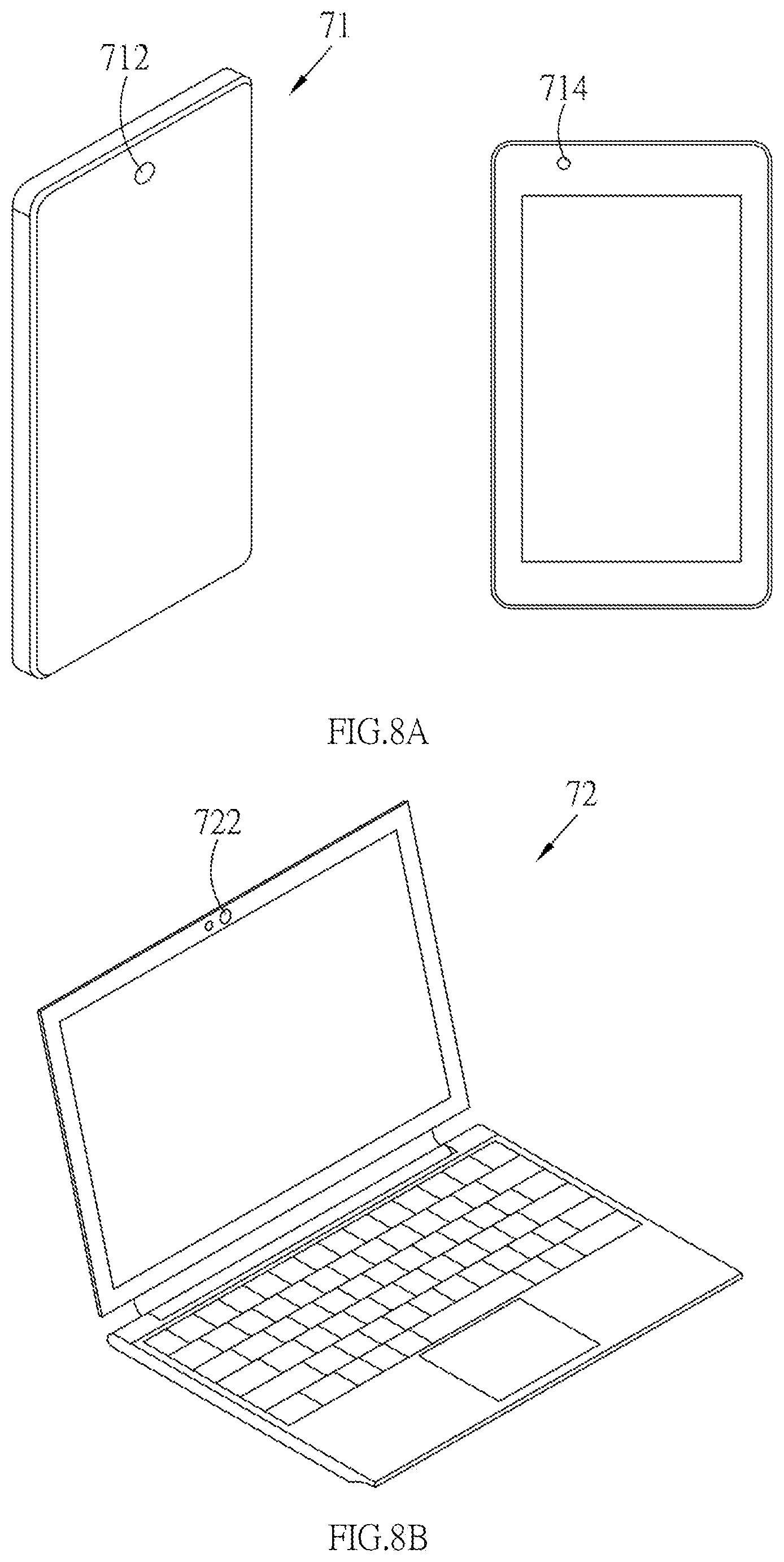
[0060] FIG. 8A is a schematic diagram, showing the optical image capturing module of the present invention is applied to the mobile communication device;
[0061] FIG. 8B is a schematic diagram, showing the optical image capturing module of the present invention is applied to the mobile information device;
[0062] FIG. 8C is a schematic diagram, showing the optical image capturing module of the present invention is applied to the smart watch;
[0063] FIG. 8D is a schematic diagram, showing the optical image capturing module of the present invention is applied to the smart head-wearing device;
[0064] FIG. 8E is a schematic diagram, showing the optical image capturing module of the present invention is applied to the safety monitoring device;
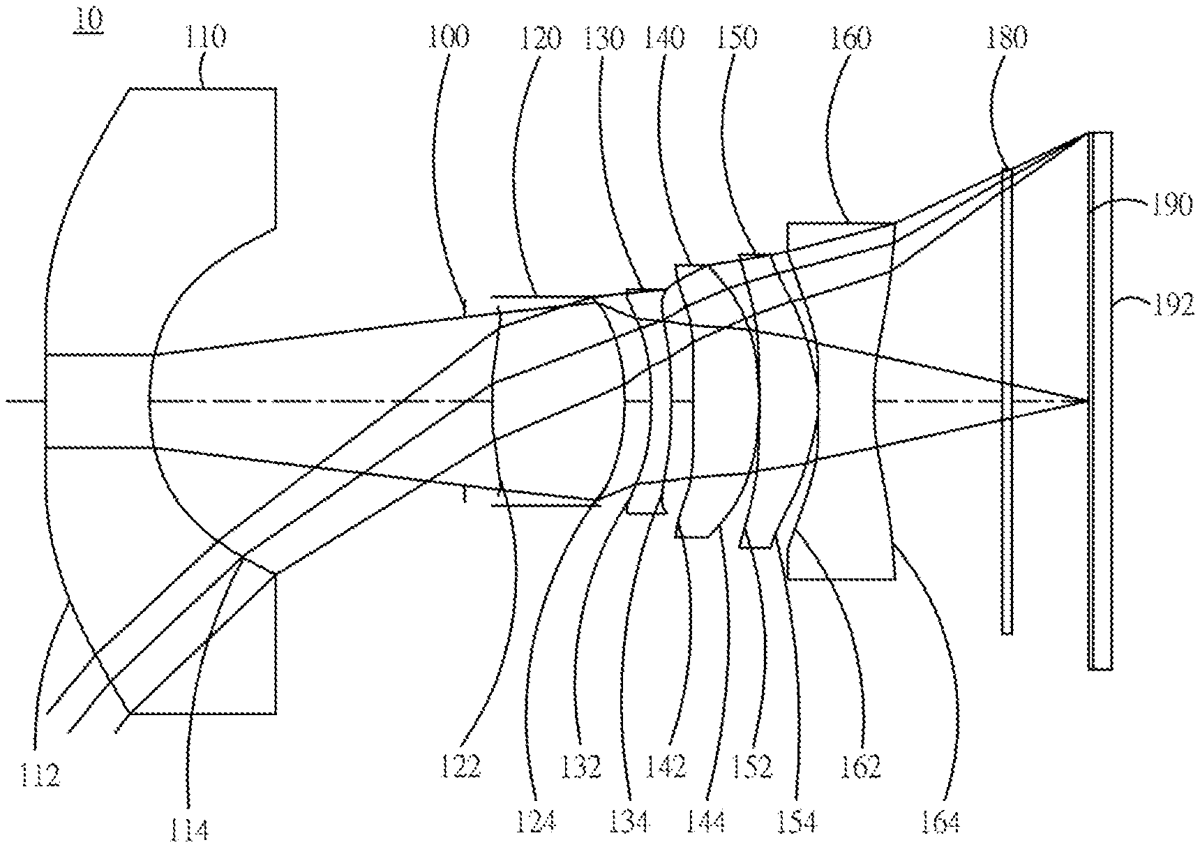
[0065] FIG. 8F is a schematic diagram, showing the optical image capturing module of the present invention is applied to the vehicle image device;
[0066] FIG. 8G is a schematic diagram, showing the optical image capturing module of the present invention is applied to the unmanned aircraft device;
[0067] FIG. 8H is a schematic diagram, showing the optical image capturing module of the present invention is applied to the extreme sport image device.
DETAILED DESCRIPTION OF THE INVENTION
[0068] An optical image capturing module of the present invention includes a structural design and an optical design, wherein structural embodiments will be described first.
[0069] As shown in FIG. 1A, an optical image capturing module according to a first structural embodiment of the present invention includes mainly includes a circuit assembly and a lens assembly. The circuit assembly includes an image sensing component S and a circuit substrate EB. A maximum value of a minimum length of an outer periphery of the image sensing component S which is perpendicular to a plane of an optical axis of the lens assembly is denoted by LS. In the current embodiment, the image sensing component S is fixed on the circuit substrate EB in a packaging mode. More specifically, the circuit substrate EB has an upper surface ESU and a lower surface ESD, which are located oppositely, and has a through hole EH penetrating through the upper surface ESU and the lower surface ESD, wherein the lower surface ESD of the circuit substrate EB has sensing surface, wherein a surface of the image sensing component S has a plurality of image contacts IP on the same side with the sensing surface. Each of the image contacts IP is electrically connected to one of the circuit contacts EP on the circuit substrate EB via a signal transmission element SC, so that the image sensing component S is fixed on an outside of the lower surface ESD of the circuit substrate EB, and the sensing surface directly faces the through hole EH. In the current embodiment, each of the signal transmission elements SC is a solder ball. In this way, when an image optical signal is sensed by the sensing surface of the image sensing component S and is transformed into an electrical signal, the electrical signal could be sent to the circuit contacts EP via the image contacts IP and the signal transmission elements SC, so that the circuit contacts EP could transmit the electrical signal to other external components for subsequent processing.
[0070] The lens assembly includes a fixed base FB1, a movable base MB1, a lens group L, and an IR-cut filter IR1. In the current embodiment, the fixed base FB1 is made of plastic material and is opaque, and has a focusing hole penetrating through both ends of the fixed base FB1, so that the fixed base FB1 is hollow. The fixed base FB1 is disposed on the upper surface ESU of the circuit substrate EB, so that the image sensing component S directly faces the focusing hole via the through hole EH. The movable base MB1 has a receiving hole penetrating through both ends of the movable base MB1, so that the movable base MB1 is hollow, wherein the receiving hole directly faces the sensing surface of the image sensing component S. More specifically, the movable base MB1 includes an inner holder LH1 and a lens barrel B1, wherein the inner holder LH1 is disposed in the fixed base FB1 and is located in the focusing hole, and is controllable to move relative to the fixed base FB1. The inner holder LH1 has an inner through hole DH1 penetrating through both ends of the inner holder LH1, so that the inner holder LH1 is hollow. The lens barrel B1 is disposed in the inner holder LH1 and is located in the inner through hole DH1, and is capable of being driven by the inner holder LH1 to move relative to the fixed base FB1. The lens barrel B1 has the receiving hole penetrating through both ends of the lens barrel B1, so that the lens barrel B1 is hollow.
[0071] The fixed base FB1 has a predetermined thickness TH1 (i.e., a distance from an outer wall of the fixed base FB1 to an inner wall of the inner through hole of the inner holder LH1 in a direction perpendicular to the optical axis of the lens group L), and a maximum value of a minimum length on a periphery of the fixed base FB1 perpendicular to the optical axis of the lens group L is denoted by PhiD. In addition, the lens barrel B1 has a predetermined thickness TH2 (i.e., a minimum thickness), and a maximum value of a minimum length on a periphery of the lens barrel B1 perpendicular to the optical axis of the lens group L is denoted by PhiC. In the current embodiment, a glue is coated between the lens barrel BI and the inner holder LH1, and the lens barrel B1 and the inner holder LH1 are fixed to each other via the glue, so that the lens barrel B1 is disposed in the inner holder LHI and is fixed in the inner through hole DH1.
[0072] The lens group L includes at least two lenses with refractive power, and optical embodiments will be described in detail later. The lens group L is disposed on the lens barrel BI of the movable base MB1 and is located in the receiving hole. In addition, an image plane of the lens group L is adjustable to be located on the sensing surface of the image sensing component S along with a movement of the movable base MB1, wherein the optical axis of the lens group L overlaps with a central normal of the sensing surface, so that light could pass through the lens group L in the receiving hole and the through hole EH of the circuit substrate EB, and could be projected onto the sensing surface. Moreover, a maximum diameter of an image-side surface of a lens of the lens group L closest to the image plane is denoted by PhiB, and a maximum effective diameter of the image-side surface of the lens of the tens group L closest to the image plane (i.e., the image space) could be also called optical exit pupil, and is denoted by PhiA.
[0073] The IR-cut filter IR1 is fixed on the circuit substrate EB and covers the through hole EH, so that the IR-cut filter IR1 is located above the image sensing component S and is located between the lens group L and the image sensing component S, thereby to filter out an excess infrared in the image light passing through the lens group L, enhancing the image quality. In practice, the IR-cut filter IR1 could be fixed on the fixed base FB1 or on the movable base MB1.
[0074] It is worth mentioning that, in order to overlap the optical axis of the lens group L with the central normal of the sensing surface of the image sensing component S, an outer side of the lens barrel B1 of the optical image capturing module of the current embodiment is not completely in contact with an inner periphery of the inner holder LH1, thereby to leave a slight gap, so that a curable glue could be coated between the inner holder LH1 and the lens barrel B1 in advance, and the optical axis of the lens group L and the central normal of the image sensing component S could be adjusted to be overlapped with each other, and then the curable glue is cured to fix the lens barrel B1 to the inner holder LH1, that is, an active alignment assembly is carried out. The precision optical image capturing modules or special applications (such as the assembly of multiple lenses) require the active alignment technology, and the optical image capturing module of the present invention could meet such requirement. It is worth mentioning that, the image sensing component S is located outside of the lower surface ESD of the circuit substrate EB, which could increase a back focal length and improve the optical quality.
[0075] In order to keep small in size and provide high imaging quality, the optical image capturing module of the current embodiment satisfies:
[0076] 0 mm<PhiA.ltoreq.17.4 mm; 0 mm<PhiC.ltoreq.17.7 mm; 0 mm<PhiD.ltoreq.18 mm; 0 mm<TH1.ltoreq.5 mm; 0 mm<TH2.ltoreq.5 mm; 0<PhiA/PhiD.ltoreq.0.99; 0 mm<TH1+TH2.ltoreq.1.5 mm; and 0<2*(TH1+TH2)/PhiA.ltoreq.0.95.
[0077] Preferably, the optical image capturing module of the current embodiment satisfies:
[0078] 0 mm<PhiA.ltoreq.13.5 mm; 0 mm<PhiC.ltoreq.14 mm; 0 mm<PhiD.ltoreq.1.5 mm; 0 mm<TH1.ltoreq.0.5 mm; 0 mm<TH2.ltoreq.0.5 mm; 0<PhiA/PhiD.ltoreq.0.97; 0 mm<TH1+TH2.ltoreq.1 mm; and 0<2*(TH1+TH2)/PhiA.ltoreq.0.5.
[0079] As shown in FIG. 1B to FIG. 1D, optical image capturing modules according to a second structural embodiment to a fourth structural embodiment are illustrated, each of which is slightly different from that of the first structural embodiment, but the effect of miniaturization and high optical quality could be achieved as well.
[0080] The optical image capturing modules according to the second structural embodiment is illustrated in FIG. 1B, which has almost the same structure with that of the first structural embodiment, except that an outer peripheral wall of a lens barrel B2 has an external thread OT2 thereon, and an inner wall of an inner through hole DH2 of an inner holder LH2 has an inner thread IT2 thereon, wherein the inner thread IT2 is adapted to be screwed with the external thread OT2, thereby to fix the lens barrel B2 in the inner holder LH2. In addition, the optical image capturing modules according to the second structural embodiment satisfies the conditions of the first structural embodiment, which could keep small in size and provide high imaging quality as well.
[0081] The optical image capturing modules according to the third structural embodiment is illustrated in FIG. 1C, which has almost the same structure with that of the first structural embodiment, except that a movable base MB3 is integrally formed as a monolithic unit, instead of being separated to a lens barrel and an inner holder, which reduces the time required for producing components and for assembling.
[0082] Moreover, the optical image capturing modules according to the third structural embodiment satisfies 0 mm<PhiA.ltoreq.17.4 mm, and a preferable range is 0 mm<PhiA.ltoreq.13.5 mm; 0 mm<PhiD.ltoreq.18 mm, and a preferable range is 0 mm<PhiD.ltoreq.15 mm; 0<PhiA/PhiD.ltoreq.0.99, and a preferable range is 0<PhiA/PhiD.ltoreq.0.97; 0 mm<TH1+TH2.ltoreq.1.5 mm, and a preferable range is 0 mm<TH1+TH2.ltoreq.1 mm; 0<2*(TH1+TH2)/PhiA.ltoreq.0.95, and a preferable range is 0<2*(TH1+TH2)/PhiA.ltoreq.0.5. In other words, the optical image capturing modules according to the third structural embodiment satisfies partially of the conditions of the first structural embodiment, which could keep small in size and provide high imaging quality as well.
[0083] The optical image capturing modules according to the fourth structural embodiment is illustrated in FIG. 1D, which has almost the same structure with that of the first structural embodiment, except that the circuit assembly further includes a bracket BH, wherein the bracket BH has a recess BHS. A portion of the bracket BH around an opening of the recess BHS is connected to the lower surface ESD of the circuit substrate EB, wherein the image sensing component S is located in the recess BHS. In this way, the bracket BH could support and protect the image sensing component S. In addition, when the signal transmission element SC is softened by heat during the assembly process, a relative position of the image sensing component S and the circuit substrate EB could be facilitated to control. In addition, the optical image capturing modules according to the fourth structural embodiment satisfies the conditions of the first structural embodiment, and could be fixed by a glue to carry out the active alignment assembly, which could keep small in size and provide high imaging quality as well. The bracket BH could also applied to the optical image capturing modules according to the second and third structural embodiments.
[0084] However, the signal transmission element is not limited to be a solder ball. In practice, the signal transmission element could be a projection, a pin, which are made of a conductor, or a group of their constituents, thereby to transmit the electrical signal.
[0085] Furthermore, the optical embodiments will be described in detail as follow. The optical image capturing module could work in three wavelengths, including 486.1 nm, 587.5 nm, and 656.2 nm, wherein 587.5 nm is the main reference wavelength and is the reference wavelength for obtaining the technical characters. The optical image capturing module could also work in five wavelengths, including 470 nm, 510 mn, 555 nm, 610 nm, and 650 nm wherein 555 nm is the main reference wavelength, and is the reference wavelength for obtaining the technical characters.
[0086] The optical image capturing module of the present invention satisfies 0.5.ltoreq..SIGMA.PPR/|.SIGMA.NPR|.ltoreq.15, and a preferable range is 1.ltoreq..SIGMA.PPR/|.SIGMA.NPR|.ltoreq.3.0, where PPR is a ratio of the focal length f of the optical image capturing module to a focal length fp of each of lenses with positive refractive power; NPR is a ratio of the focal length f of the optical image capturing module to a focal length fn of each of lenses with negative refractive power; .SIGMA.PPR is a sum of the PPRs of each positive lens; and .SIGMA.NPR is a sum of the NPRs of each negative lens. It is helpful for control of an entire refractive poWer and an entire length of the optical image capturing module.
[0087] The optical image capturing module further include an image sensor provided on the image plane. The optical image capturing module of the present invention satisfies HOS/HOI.ltoreq.50 and 0.5.ltoreq.HOS/f.ltoreq.150, and a preferable range is 1.ltoreq.HOS/HOI.ltoreq.40 and 1.ltoreq.HOS/f.ltoreq.140, where HOI is a half of a diagonal of an effective sensing area of the image sensor, i.e., the maximum image height, and HOS is a height of the optical image capturing module, i.e. a distance on the optical axis between the object-side surface of the first lens and the image plane. It is helpful for reduction of the size of the optical image capturing module for used in compact cameras.
[0088] The optical image capturing module of the present invention further is provided with an aperture to increase image quality.
[0089] In the optical image capturing module of the present invention, the aperture could be a front aperture or a middle aperture, wherein the front aperture is provided between the object and the first lens, and the middle is provided between the first lens and the image plane. The front aperture provides a long distance between an exit pupil of the optical image capturing module and the image plane, which allows more elements to be installed. The middle could enlarge a view angle of view of the optical image capturing module and increase the efficiency of, the image sensor. The optical image capturing module satisfies 0.1.ltoreq.InS/HOS.ltoreq.1.1, where InS is a distance between the aperture and the image surface. It is helpful for size reduction and wide angle.
[0090] The optical image capturing module of the present invention satisfies 0.1.ltoreq..SIGMA.TP/InTL.ltoreq.0.9, where InTL is a distance between the object-side surface of the first lens and the image-side surface of the sixth lens, and .SIGMA.TP is a sum of central thicknesses of the lenses on the optical axis. It is helpful for the contrast of image and yield rate of manufacture and provides a suitable back focal length for installation of other elements. In addition, the optical image capturing module of the present invention satisfies 0.1.ltoreq.InTL/HOS.ltoreq.0.95, which is helpful for reduction of the size of the optical image capturing module for used in compact cameras.
[0091] The optical image capturing system has a maximum image height HOI on the image plane vertical to the optical axis. A transverse aberration at 0.7 HOI in the positive direction of the tangential ray fan aberration after the longest operation wavelength of visible light passing through the edge of the entrance pupil is denoted by PLTA; a transverse aberration at 0.7 HOI in the positive direction of the tangential ray fan aberration after the shortest operation wavelength of visible light passing through the edge of the entrance pupil is denoted by PSTA; a transverse aberration at 0.7 HOI in the negative direction of the tangential ray fan aberration finer the longest operation wavelength of visible light passing through the edge of the entrance pupil is denoted by NLTA; a transverse aberration at 0.7 HOI in the negative direction of the tangential ray fan aberration after the shortest operation wavelength of visible light passing through the edge of the entrance pupil is denoted by NSTA; a transverse aberration at 0.7 HOI of the sagittal ray fan aberration after the longest operation wavelength of visible light passing through the edge of the entrance pupil is denoted by SLTA; a transverse aberration at 0.7 HOI of the sagittal ray fan aberration after the shortest operation wavelength of visible light passing through the edge of the entrance pupil is denoted by SSTA. In addition, the optical image capturing module has a better image performance when the optical image capturing module of the present invention satisfies PLTA.ltoreq.100 .mu.m; PSTA.ltoreq.100 .mu.m; NLTA.ltoreq.100 .mu.m; NSTA.ltoreq.100 .mu.m; SLTA.ltoreq.100 .mu.m; and SSTA.ltoreq.100 .mu.m.
[0092] The optical image capturing module of the present invention satisfies 0.001.ltoreq.|R1/R2|.ltoreq.25, and a preferable range is 0.01.ltoreq.|R1/R2|.ltoreq.12, where R1 is a radius of curvature of the object-side surface of the first lens, and R2 is a radius of curvature of the image-side surface of the first lens. It provides the first lens with a suitable positive refractive power to reduce the increase rate of the spherical aberration.
[0093] The optical image capturing module of the present invention satisfies -7<(R11-R12)/(R11+R12)<50, where R11 is a radius of curvature of the object-side surface of the sixth lens, and R12 is a radius of curvature of the image-side surface of the sixth lens. It may modify the astigmatic field curvature.
[0094] The optical image capturing module of the present invention satisfies IN12/f.ltoreq.60, where IN12 is a distance on the optical axis between the first lens and the second lens. It may correct chromatic aberration and improve the performance.
[0095] The optical image capturing module of the present invention satisfies IN56/f.ltoreq.3.0, where IN56 is a distance on the optical axis between the fifth lens and the sixth lens. It may correct chromatic aberration and improve the performance.
[0096] The optical image capturing module of the present invention satisfies 0.1.ltoreq.(TP1+IN12)/TP2.ltoreq.10, where TP1 is a central thickness of the first lens on the optical axis, and TP2 is a central thickness of the second lens on the optical axis. It may control the sensitivity of manufacture of the optical image capturing module and improve the performance.
[0097] The optical image capturing module of the present invention satisfies 0.1.ltoreq.(TP6+IN56)/TP5.ltoreq.15, where TP5 is a central thickness of the fifth lens on the optical axis, TP6 is a central thickness of the sixth lens on the optical axis, and IN56 is a distance between the fifth lens and the sixth lens. It may control the sensitivity of manufacture of the optical image capturing module and improve the performance.
[0098] The optical image capturing module of the present invention satisfies 0.1.ltoreq.TP4/(IN34+TP4+IN45)<1 where TP2 is a central thickness of the second lens on the optical axis, TP3 is a central thickness of the third lens on the optical axis, TP4 is a central thickness of the fourth lens on the optical axis, IN34 is a distance on the optical axis between the third lens and the fourth lens, IN45 is a distance on the optical axis between the fourth lens and the fifth lens, and InTL is a distance between the object-side surface of the first lens and the image-side surface of the seventh lens. It may fine tune and correct the aberration of the incident rays layer by layer, and reduce the height of the optical image capturing module.
[0099] The optical image capturing module satisfies 0 mm.ltoreq.HVT61.ltoreq.3 mm; 0 mm<HVT62.ltoreq.6 mm; 0.ltoreq.HVT61/HVT62; 0 mm.ltoreq.|SGC61|.ltoreq.0.5 mm; 0 mm<|SGC62|.ltoreq.2 mm; and 0<|SGC62|/(|SGC62|+TP6).ltoreq.0.9, where HVT61 a distance perpendicular to the optical axis between the critical point C61 on the object-side surface of the sixth lens and the optical axis; HVT62 a distance perpendicular to the optical axis between the critical point C62 on the image-side surface of the sixth lens and the optical axis; SGC61 is a distance on the optical axis between a point on the object-side surface of the sixth lens where the optical axis passes through and a point where the critical point C61 projects on the optical axis; SGC62 is a distance on the optical axis between a point on the image-side surface of the sixth lens where the optical axis passes through and a point where the critical point C62 projects on the optical axis. It is helpful to correct the off-axis view field aberration.
[0100] The optical image capturing module satisfies 0.2.ltoreq.HVT62/HOI.ltoreq.0.9, and preferably satisfies 0.3.ltoreq.HVT62/HOS.ltoreq.0.8. It may help to correct the peripheral aberration.
[0101] The optical image capturing module satisfies 0.ltoreq.HVT62/HOS.ltoreq.0.5, and preferably satisfies 0.2.ltoreq.HVT62/HOS.ltoreq.0.45. It may help to correct the peripheral aberration.
[0102] The optical image capturing module of the present invention satisfies 0<SGI611/(SGI611+TP6).ltoreq.0.9; 0<SGI621/(SGI621+TP6).ltoreq.0.9, and it is preferable to satisfy 0.1<SGI611/(SGI611+TP6).ltoreq.0.6; 0.1<SGI621/(SGI621+TP7).ltoreq.0.6, where SGI611 is a displacement on the optical axis from a point on the object-side surface of the sixth lens, through which the optical axis passes, to a point where the inflection point on the object-side surface, which is the closest to the optical axis, projects on the optical axis, and SGI621 is a displacement on the optical axis from a point on the image-side surface of the sixth lens, through which the optical axis passes, to a point where the inflection point on the image-side surface, which is the closest to the optical axis, projects on the optical axis.
[0103] The optical image capturing module of the present invention satisfies 0<SGI612/(SGI612+TP6).ltoreq.0.9; 0<SGI622/(SGI622+TP6).ltoreq.0.9, and it is preferable to satisfy 0.1<SGI612/(SGI612+TP6).ltoreq.0.6; 0.1.ltoreq.SGI622/(SGI622+TP6).ltoreq.0.6, where SGI612 is a displacement on the optical axis from a point on the object-side surface of the sixth lens, through which the optical axis passes, to a point where the inflection point on the object-side surface, which is the second closest to the optical axis, projects on the optical axis, and SGI622 is a displacement on the optical axis from a point on the image-side surface of the sixth lens, through which the optical axis passes, to a point where the inflection point on the object-side surface, which is the second closest to the optical axis, projects on the optical axis.
[0104] The optical image capturing module of the present invention satisfies 0.001 mm.ltoreq.|HIF611|.ltoreq.5 mm; 0.001 mm.ltoreq.|HIF621|.ltoreq.5, mm, and it is preferable to satisfy 0.1 mm.ltoreq.|HIF611|.ltoreq.3.5 mm; 1.5 mm.ltoreq.|HIF621|.ltoreq.3.5 mm, where HIF611 is a distance perpendicular to the optical axis between the inflection point on the object-side surface of the sixth lens, which is the closest to the optical axis, and the optical axis; HIF621 is a distance perpendicular to the optical axis between the inflection point on the image-side surface of the sixth lens, which is the closest to the optical axis, and the optical axis.
[0105] The optical image capturing module of the present invention satisfies 0.001 mm.ltoreq.|HIF612|.ltoreq.5 mm; 0.001 mm.ltoreq.|HIF622|.ltoreq.5 mm, and it is preferable to satisfy 0.1 mm.ltoreq.|HIF622|.ltoreq.3.5 mm; 0.1 mm.ltoreq.|HIF612|.ltoreq.3.5 mm, where HIF612 is a distance perpendicular to the optical axis between the inflection point on the object-side surface of the sixth lens, which is the second closest to the optical axis, and the optical axis; HIF622 is a distance perpendicular to the optical axis between the inflection point on the image-side surface of the sixth lens, which is the second closest to the optical axis, and the optical axis.
[0106] The optical image capturing module of the present invention satisfies 0.001 mm.ltoreq.|HIF613|.ltoreq.5 mm; 0.001 mm.ltoreq.|HIF623|.ltoreq.5 mm, and it is preferable to satisfy 0.1 mm.ltoreq.|HIF623|.ltoreq.3.5 mm; 0.1 mm.ltoreq.|HIF613|.ltoreq.3.5 mm, where HIF613 is a distance perpendicular to the optical axis between the inflection point on the object-side surface of the sixth lens, which is the third closest to the optical axis, and the optical axis; HIF623 is a distance perpendicular to the optical axis between the inflection point on the image-side surface of the sixth lens, which is the third closest to the optical axis, and the optical axis.
[0107] The optical image capturing module of the present invention satisfies 0.001 mm.ltoreq.|HIF614|.ltoreq.5 mm; 0.001 mm.ltoreq.|HIF624|.ltoreq.5 mm, and it is preferable to satisfy 0.1 mm; 0.1 mm.ltoreq.|HIF614|.ltoreq.3.5 mm, where HIF614 is a distance perpendicular to the optical axis between the inflection point on the object-side surface of the sixth lens, which is the fourth closest to the optical axis, and the optical axis; HIF624 is a distance perpendicular to the optical axis between the inflection point on the image-side surface of the sixth lens, which is the fourth closest to the optical axis, and the optical axis.
[0108] The optical image capturing module of the present invention satisfies 0<(TH1-TH2)/HOI.ltoreq.0.95; 0<(TH1+TH2)/HOS.ltoreq.0.95; 0<2*(TH1+TH2)/PhiA.ltoreq.0.95; and it is preferable to satisfy 0<(TH1+TH2)/HOI.ltoreq.0.5; 0<(TH1-TH2)/HOS.ltoreq.0.5; 0<2*(TH1+TH2)/PhiA.ltoreq.0.5.
[0109] In an embodiment, the lenses of high Abbe number and the lenses of low Abbe number are arranged in an interlaced arrangement that could be helpful for correction of aberration of the optical image capturing module.
[0110] An equation of aspheric surface is
z=ch.sup.2/[1+[1(k+1)c.sup.2h.sup.2].sup.0.5]+A4h.sup.4+A6h.sup.6+A8h.su- p.8+A10h.sup.10+A12h.sup.12+A14h.sup.14+A16h.sup.16+A18h.sup.18+A20h.sup.2- 0+ (1)
[0111] where z is a depression of the aspheric surface; k is conic constant; c is reciprocal of the radius of curvature; and A4, A6, A8, A10, A12, A14, A16, A18, and A20 are high-order aspheric coefficients.
[0112] In the optical image capturing module, the lenses could be made of plastic or glass. The plastic lenses may reduce the weight and lower the cost of the optical image capturing module, and the glass lenses may control the thermal effect and enlarge the space for arrangement of the refractive power of the optical image capturing module. In addition, the opposite surfaces (object-side surface and image-side surface) of the first to the seventh lenses could be aspheric that could obtain more control parameters to reduce aberration. The number of aspheric glass lenses could be less than the conventional spherical glass lenses, which is helpful for reduction of the height of the optical image capturing module.
[0113] When the lens has a convex surface, which means that the surface is convex around a position, through which the optical axis passes, and when the lens has a concave surface, which means that the surface is concave around a position, through which the optical axis passes.
[0114] The optical image capturing module of the present invention could be applied in a dynamic focusing optical image capturing module. It is superior in the correction of aberration and high imaging quality so that it could be allied in lots of fields.
[0115] The optical image capturing module of the present invention could further include a driving module to meet different demands, wherein the driving module could be coupled with the movable base and the lenses to move the lenses. The driving module could be a voice coil motor (VCM), which is used to move the lens for focusing, or could be an optical image stabilization (OIS) component, which is used to lower the possibility of having the problem of image blurring which is caused by subtle movements of the lens while shooting.
[0116] To meet different requirements, at least one lens among the first lens to the seventh lens of the optical image capturing module of the present invention could be a light filter, which filters out light of wavelength shorter than 500 nm. Such effect could be achieved by coating on at least one surface of the lens, or by using materials capable of filtering out short waves to make the lens.
[0117] To meet different requirements, the image plane of the optical image capturing module in the present invention could be either flat or curved. If the image plane is curved (e.g., a sphere with a radius of curvature), the incidence angle required for focusing light on the image plane could be decreased, which is not only helpful to shorten the length of the optical image capturing module (TTL), but also helpful to increase the relative illuminance.
[0118] We provide several optical embodiments--in conjunction with the accompanying drawings for the best understanding. In practice, the optical embodiments of the present invention could be applied to other structural embodiments.
First Optical Embodiment
[0119] As shown in FIG. 2A and FIG. 2B, an optical image capturing module 10 of the first optical embodiment of the present invention includes, along an optical axis from an object side to an image side, a first lens 110, an aperture 100, a second lens 120, a third lens 130, a fourth lens 140, a fifth lens 150, a sixth lens 160, an IR-cut filter 180, an image plane 190, and an image sensor 192.
[0120] The first lens 110 has negative refractive power and is made of plastic. An object-side surface 112 thereof, which faces the object side, is a concave aspheric surface, and an image-side surface 114 thereof, which faces the image side, is a concave aspheric surface. The object-side surface 112 has two inflection points. A profile curve length of the maximum effective half diameter of the object-side surface 112 of the first lens 110 is denoted by ARS11, and a profile curve length of the maximum effective half diameter of the image-side surface 114 of the first lens 110 is denoted by ARS12. A profile curve length of a half of the entrance pupil diameter (HEP) of the object-side surface 112 of the first lens 110 is denoted by ARE11, and a profile curve length of a half of the entrance pupil diameter (HEP) of the image-side surface 114 of the first lens 110 is denoted by ARE12. A thickness of the first lens 110 on the optical axis is denoted by TP1.
[0121] The first lens satisfies SGI111=-0.0031 nun; |SGI111|/(|SGI111|+TP1)=0.0016, where a displacement on the optical axis from a point on the object-side surface 112 of the first lens 110, through which the optical axis passes, to a point where the inflection point on the object-side surface 112, which is the closest to the optical axis, projects on the optical axis, is denoted by SGI111, and a displacement on the optical axis from a point on the image-side surface 114 of the first lens 110, through which the optical axis passes, to a point where the inflection point on the image-side surface 114, which is the closest to the optical axis, projects on the optical axis is denoted by SGI121.
[0122] The first lens 110 satisfies SGI112=1.3178 mm; |SGI121|/(|SGI112|+TP1)=0.4052, where a displacement on the optical axis from a point on the object-side surface 112 of the first lens 110, through which the optical axis passes, to a point where the inflection point on the object-side surface 112, which is the second closest to the optical axis, projects on the optical axis, is denoted by SGI112, and a displacement on the optical axis from a point on the image-side surface 114 of the first lens 110, through which the optical axis passes, to a point where the inflection point on the image-side surface 114, which is the second closest to the optical axis, projects on the optical axis is denoted by SGI122.
[0123] The first lens 110 satisfies HIF111=0.5557 mm; HIF111/HOI=0.1111, where a displacement perpendicular to the optical axis from a point on the object-side surface 112 of the first lens 110, through which the optical axis passes, to the inflection point, which is the closest to the optical axis is denoted by HIF111, and a displacement perpendicular to the optical axis from a point on the image-side surface 114 of the first lens 110, through which the optical axis passes, to the inflection point, which is the closest to the optical axis is denoted by HIF121.
[0124] The first lens 110 satisfies HIF112=5.3732 mm; HIF112/HOI=1.0746, where a displacement perpendicular to the optical axis from a point on the object-side surface 112 of the first lens 110, through which the optical axis passes, to the inflection point, which is the second closest to the optical axis is denoted by HIF 112, and a displacement perpendicular to the optical axis from a point on the image-side surface 114 of the first lens 110, through which the optical axis passes, to the inflection point, which is the second closest to the optical axis is denoted by HF122.
[0125] The second lens 120 has positive refractive power and is made of plastic. An object-side surface 122 thereof, which faces the object side, is a convex aspheric surface, and an image-side surface 124 thereof, which faces the image side, is a convex aspheric surface. The object-side surface 122 has an inflection point. A profile curve length of the maximum effective half diameter of the object-side surface 122 of the second lens 120 is denoted by ARS21, and a profile curve length of the maximum effective half diameter of the image-side surface 124 of the second lens 120 is denoted by ARS22. A profile curve length of a half of the entrance pupil diameter (HEP) of the object-side surface 122 of the second lens 120 is denoted by ARE21, and a profile curve length of a half of the entrance pupil diameter (HEP) of the image-side surface 124 of the second lens 120 is denoted by ARE22. A thickness of the second lens 120 on the optical axis is denoted by TP2.
[0126] The second lens 120 satisfies SGI211=0.1069 mm; |SGI211|/(|SGI211|+TP2)=0.0412; SGI221=0 mm; |ISGI221|/(|SGI221|+TP2)=0, where a displacement on the optical axis from a point on the object-side surface 122 of the second lens 120, through which the optical axis passes, to a point where the inflection point on the object-side surface 122, which is the closest to the optical axis, projects on the optical axis, is denoted by SGI211, and a displacement on the optical axis from a point on the image-side surface 124 of the second lens 120, through which the optical axis passes, to a point where the inflection point on the image-side surface 124, which is the closest to the optical axis, projects on the optical axis is denoted by SGI221.
[0127] The second lens 120 satisfies HIF211=1.1264 mm; HIF211/HOI=0.2253; HIF221=0 mm; HIF221/HOI=0, where a displacement perpendicular to the optical axis from a point on the object-side surface 122 of the second lens 120, through which the optical axis passes, to the inflection point, which is the closest to the optical axis is denoted by HIF211, and a displacement perpendicular to the optical axis from a point on the image-side surface 124 of the second lens 120, through which the optical axis passes, to the inflection point, which is the closest to the optical axis is denoted by HIF221.
[0128] The third lens 130 has negative refractive power and is made of plastic. An object-side surface 132, which faces the object side, is a concave aspheric surface, and an image-side surface 134, which faces the image side, is a convex aspheric surface. The object-side surface 132 has an inflection point, and the image-side surface 134 has an inflection point. The object-side surface 122 has an inflection point. A profile curve length of the maximum effective half diameter of the object-side surface 132 of the third lens 130 is denoted by ARS31, and a profile curve length of the maximum effective half diameter of the image-side surface 134 of the third lens 130 is denoted by ARS32. A profile curve length of a half of the entrance pupil diameter (HEP) of the object-side surface 132 of the third lens 130 is denoted by ARE31, and a profile curve length of a half of the entrance pupil diameter (HEP) of the image-side surface 134 of the third lens 130 is denoted by ARS32. A thickness of the third lens 130 on the optical axis is denoted by TP3.
[0129] The third lens 130 satisfies SGI311=-0.3041 mm; |SGI311|/(|SGI311|+TP3)=0.4445; SGI321=-0.1172 mm; |SGI321|/(|SGI321|+TP3)=0.2357, where SGI311 is a displacement on the optical axis from a point on the object-side surface 132 of the third lens 130, through which the optical axis passes, to a point where the inflection point on the object-side surface 132, which is the closest to the optical axis, projects on the optical axis, and SGI321 is a displacement on the optical axis from a point on the image-side surface 134 of the third lens 130, through which the optical axis passes, to a point where the inflection point on the image-side surface 134, which is the closest to the optical axis, projects on the optical axis.
[0130] The third lens 130 satisfies HIF311=1.5907 mm; HIF311/HOI=0.3181; HIF321=1.3380 mm; HIF321/HOI=0.2676, where HIF311 is a distance perpendicular to the optical axis between the inflection point on the object-side surface 132 of the third lens 130, which is the closest to the optical axis, and the optical axis; HIF321 is a distance perpendicular to the optical axis between the inflection point on the image-side surface 134 of the third lens 130, which is the closest to the optical axis, and the optical axis.
[0131] The fourth lens 140 has positive refractive power and is made of plastic. An object-side surface 142, which faces the object side, is a convex aspheric surface, and an image-side surface 144, which faces the image side, is a concave aspheric surface. The object-side surface 142 has two inflection points, and the image-side surface 144 has an inflection point. A profile curve length of the maximum effective half diameter of the object-side surface 142 of the fourth lens 140 is denoted by ARS41, and a profile curve length of the maximum effective half diameter of the image-side surface 144 of the fourth lens 140 is denoted by ARS42. A profile curve length of a half of the entrance pupil diameter (HEP) of the object-side surface 142 of the fourth lens 140 is denoted by ARE41, and a profile curve length of a half of the entrance pupil diameter (HEP) of the image-side surface 144 of the fourth lens 140 is denoted by ARE42. A thickness of the fourth lens 140 on the optical axis is TP4.
[0132] The fourth lens 140 satisfies SGI411=0.0070 mm; |SGI411|/(|SGI411|+TP4)=0.0056; SGI421=0.0006 mm; |SGI421|/(|SGI421|+TP4)=0.0005, where SGI411 is a displacement on the optical axis from a point on the object-side surface 142 of the fourth lens 140, through which the optical axis passes, to a point where the inflection point on the object-side surface 142, which is the closest to the optical axis, projects on the optical axis, and SGI421 is a displacement on the optical axis from a point on the image-side surface 144 of the fourth lens 140, through which the optical axis passes, to a point where the inflection point on the image-side surface 144, which is the closest to the optical axis, projects on the optical axis.
[0133] The fourth lens 140 satisfies SGI412=-0.2078 mm; |SGI412|/(|SGI412|+TP4)=0.1439, where SGI412 is a displacement on the optical axis from a point on the object-side surface 142 of the fourth lens 140, through which the optical axis passes, to a point where the inflection point on the object-side surface 142, which is the second closest to the optical axis, projects on the optical axis, and SGI422 is a displacement on the optical axis from a point on the image-side surface 144 of the fourth lens 140, through which the optical axis passes, to a point where the inflection point on the image-side surface 144, which is the second closest to the optical axis, projects on the optical axis.
[0134] The fourth lens 140 further satisfies HIF411=0.4706 mm; HIF411/HOI=0.0941; HIF421=0.1721 mm; HIF421/HOI=0.0344, where HIF411 is a distance perpendicular to the optical axis between the inflection point on the object-side surface 142 of the fourth lens 140, which is the closest to the optical axis, and the optical axis; HIF421 is a distance perpendicular to the optical axis between the inflection point on the image-side surface 144 of the fourth lens 140, which is the closest to the optical axis, and the optical axis.
[0135] The fourth lens 140 satisfies HIF412=2.0421 mm; HIF412/HOI=0.4084, where HIF412 is a distance perpendicular to the optical axis between the inflection point on the object-side surface 142 of the fourth lens 140, which is the second closest to the optical axis, and the optical axis; HIF422 is a distance perpendicular to the optical axis between the inflection point on the image-side surface 144 of the fourth lens 140, which is the second closest to the optical axis, and the optical axis.
[0136] The fifth lens 150 has positive refractive power and is made of plastic. An object-side surface 152, which faces the object side, is a convex aspheric surface, and an image-side surface 154, which faces the image side, is a convex aspheric surface. The object-side surface 152 has two inflection points, and the image-side surface 154 has an inflection point. A profile curve length of the maximum effective half diameter of the object-side surface 152 of the fifth lens 150 is denoted by ARS51, and a profile curve length of the maximum effective half diameter of the image-side surface 154 of the fifth lens 150 is denoted by ARS52. A profile curve length of a half of the entrance pupil diameter (HEP) of the object-side surface 152 of the fifth lens 150 is denoted by ARE51, and a profile curve length of a half of the entrance pupil diameter (HEP) of the image-side surface 154 of the fifth lens 150 is denoted by ARE52. A thickness of the fifth lens 150 on the optical axis is denoted by TPS.
[0137] The fifth lens 150 satisfies SGI511=0.00364 mm; SGI521=-0.63365 mm; |SGI511|/(|SGI511|+TP5)=0.00338; |SGI521|/(|SGI521|+TP5)=0.37154, where SGI511 is a displacement on the optical axis from a point on the object-side surface 152 of the fifth lens 150, through which the optical axis passes, to a point where the inflection point on the object-side surface 152, which is the closest to the optical axis, projects on the optical axis, and SGI521 is a displacement on the optical axis from a point on the image-side surface 154 of the fifth lens 150, through which the optical axis passes, to a point where the inflection point on the image-side surface 154, which is the closest to the optical axis, projects on the optical axis.
[0138] The fifth lens 150 satisfies SGI512=-0.32032 mm; |SGI512|/(|SGI512|+TP5)=0.23009, where SGI512 is a displacement on the optical axis from a point on the object-side surface 152 of the fifth lens 150, through which the optical axis passes, to a point where the inflection point on the object-side surface 152, which is the second closest to the optical axis, projects on the optical axis, and SGI522 is a displacement on the optical axis from a point on the image-side surface 154 of the fifth lens 150, through which the optical axis passes, to a point where the inflection point on the image-side surface 154, which is the second closest to the optical axis, projects on the optical axis.
[0139] The fifth lens 150 satisfies SGI513=0 mm; SGI523=0 mm; |SGI513|/(|SGI513|+TP5)=0; |SGI523|/(|SGI523|+TP5)=0, where SGI513 is a displacement on the optical axis from a point on the object-side surface 152 of the fifth lens 150, through which the optical axis passes, to a point where the inflection point on the object-side surface 152, which is the third closest to the optical axis, projects on the optical axis, and SGI523 is a displacement on the optical axis from a point on the image-side surface 154 of the fifth lens 150, through which the optical axis passes, to a point where the inflection point on the image-side surface 154, which is the third closest to the optical axis, projects on the optical axis.
[0140] The fifth lens 150 satisfies SGI514=0 mm; SGI524=0 mm; |SGI514|/(|SGI514|+TP5)=0; |SGI524|/(|SGI524|+TP5)=0, where SGI514 is a displacement on the optical axis from a point on the object-side surface 152 of the fifth lens 150, through which the optical axis passes, to a point where the inflection point on the object-side surface 152, which is the fourth closest to the optical axis, projects on the optical axis, and SGI524 is a displacement on the optical axis from a point on the image-side surface 154 of the fifth lens 150, through which the optical axis passes, to a point where the inflection point on the image-side surface 154, which is the fourth closest to the optical axis, projects on the optical axis.
[0141] The fifth lens 150 further satisfies HIF511=0.28212 mm; HIF521=2.13850 mm; HIF511/HOI=0.05642; HIF521/HOI=0.42770, where HIF511 is a distance perpendicular to the optical axis between the inflection point on the object-side surface 152 of the fifth lens 150, which is the closest to the optical axis, and the optical axis; HIF52I is a distance perpendicular to the optical axis between the inflection point on the image-side surface 154 of the fifth lens 150, which is the closest to the optical axis, and the optical axis.
[0142] The fifth lens 150 further satisfies HIF512=2.51384 mm; HIF512/HOI=0.50277, where HIF512 is a distance perpendicular to the optical axis between the inflection point on the object-side surface 152 of the fifth lens 150, which is the second closest to the optical axis, and the optical axis; HIF522 is a distance perpendicular to the optical axis between the inflection point on the image-side surface 154 of the fifth lens 150, which is the second closest to the optical axis, and the optical axis.
[0143] The fifth lens 150 further satisfies HIF513=0 mm; HIF513/HOI=0; HIF523=0 mm; HIF523/HOI=0, where HIF513 is a distance perpendicular to the optical axis between the inflection point on the object-side surface 152 of the fifth lens 150, which is the third closest to the optical axis, and the optical axis; HIF523 is a distance perpendicular to the optical axis between the inflection point on the image-side surface 154 of the fifth lens 150, which is the third closest to the optical axis, and the optical axis.
[0144] The fifth lens 150 further satisfies HIF514=0 mm; HIF514/HOI=0; HIF524=0 mm; HIF524/HOI=0, where HIF514 is a distance perpendicular to the optical axis between the inflection point on the object-side surface 152 of the fifth lens 150, which is the fourth closest to the optical axis, and the optical axis; HIF524 is a distance perpendicular to the optical axis between the inflection point on the image-side surface 154 of the fifth lens 150, which is the fourth closest to the optical axis, and the optical axis.
[0145] The sixth lens 160 has negative refractive power and is made of plastic. An object-side surface 162, which faces the object side, is a concave surface, and an image-side surface 164, which faces the image side, is a concave surface. The object-side surface 162 has two inflection points, and the image-side surface 164 has an inflection point. Whereby, the incident angle of each view field entering the sixth lens 160 could be effectively adjusted to improve aberration. A profile curve length of the maximum effective half diameter of the object-side surface 162 of the sixth lens 160 is denoted by ARS61, and a profile curve length of the maximum effective half diameter of the image-side surface 164 of the sixth lens 160 is denoted by ARS62. A profile curve length of a half of the entrance pupil diameter (HEP) of the object-side surface 162 of the sixth lens 160 is denoted by ARE61, and a profile curve length of a half of the entrance pupil diameter (HEP) of the image-side surface 164 of the sixth lens 160 is denoted by ARS62. A thickness of the sixth lens 160 on the optical axis is denoted by TP6.
[0146] The sixth lens 160 satisfies SGI611=-0.38558 mm; SGI621=0.12386 mm; |SGI611|/(|SGI611|+TP6)=0.27212; |SGI621|/(|SGI621|+TP6)=0.10722, where SGI611 is a displacement on the optical axis from a point on the object-side surface 162 of the sixth lens 160, through which the optical axis passes, to a point where the inflection point on the object-side surface 162, which is the closest to the optical axis, projects on the optical axis, and SGI621 is a displacement on the optical axis from a point on the image-side surface 164 of the sixth lens 160, through which the optical axis passes, to a point where the inflection point on the image-side surface 164, which is the closest to the optical axis, projects on the optical axis.
[0147] The sixth lens 160 satisfies. SGI612=-0.47400 mm; |SGI612|/(|SGI612|+TP6)=0.31488; SGI622=0 mm; |SGI622|/(|SGI622|+TP6)=0, where SGI612 is a displacement on the optical axis from a point on the object-side surface 162 of the sixth lens 160, through which the optical axis passes, to a point where the inflection point on the object-side surface 162, which is the second closest to the optical axis, projects on the optical axis, and SGI622 is a displacement on the optical axis from a point on the image-side surface 164 of the sixth lens 160, through which the optical axis passes, to a point where the inflection point on the image-side surface 164, which is the second closest to the optical axis, projects on the optical axis.
[0148] The sixth lens 160 further satisfies HIF611=2.24283 mm; HIF621=1.07376 mm; HIF611/HOI=0.44857; HIF621/HOI=0.21475, where HIF611 is a distance perpendicular to the optical axis between the inflection point on the object-side surface 162 of the sixth lens 160, which is the closest to the optical axis, and the optical axis; HIF621 is a distance perpendicular to the optical axis between the inflection point on the image-side surface 164 of the sixth lens 160, which is the closest to the optical axis, and the optical axis.
[0149] The sixth lens 160 further satisfies HIF612=2.48895 mm; HIF612/HOI=0.49779, where HIF612 is a distance perpendicular to the optical axis between the inflection point on the object-side surface 162 of the sixth lens 160, which is the second closest to the optical axis, and the optical axis; HIF622 is a distance perpendicular to the optical axis between the inflection point on the image-side surface 164 of the sixth lens 160, which is the second closest to the optical axis, and the optical axis.
[0150] The sixth lens 160 further satisfies HIF613=0 mm; HIF613/HOI=0; HIF623=0 mm; HIF623/HOI=0, where HIF613 is a distance perpendicular to the optical axis between the inflection point on the object-side surface 162 of the sixth lens 160, which is the third closest to the optical axis, and the optical axis; HIF623 is a distance perpendicular to the optical axis between the inflection point on the image-side surface 164 of the sixth lens 160, which is the third closest to the optical axis, and the optical axis.
[0151] The sixth lens 160 further satisfies HIF614=0 mm; HIF614/HOI=0; HIF624=0 mm; HIF624/HOI=0, where HIF614 is a distance perpendicular to the optical axis between the inflection point on the object-side surface 162 of the sixth lens 160, which is the fourth closest to the optical axis, and the optical axis; HIF624 is a distance perpendicular to the optical axis between the inflection point on the image-side surface 164 of the sixth lens 160, which is the fourth closest to the optical axis, and the optical axis.
[0152] The IR-cut filter 180 is made of glass and is disposed between the sixth lens 160 and the image plane 190. The IR-cut filter 180 gives no contribution to the focal length of the optical image capturing module.
[0153] The optical image capturing module 10 of the first optical embodiment has the following parameters, which are f=4.075 mm; f/HEP=1.4; HAF=50.001 degrees; and tan(HAF)=1.1918, where f is a focal length of the lens group; HAF is a half of the maximum field angle; and HEP is an entrance pupil diameter.
[0154] The parameters of the lenses of the first optical embodiment are f1=-7.828 mm; |f/f1|=0.52060; f6=-4.886; and |f1|>f6, where f1 is a focal length of the first lens 110; and f6 is a focal length of the sixth lens 160.
[0155] The first optical embodiment further satisfies |f2|+|f3|+|f4|+|f5|=95.50815; |f1|+|f6|=12.71352 and |f2|+|f3|+|f4|+|f5|>|f1|+|f6|, where f2 is a focal length of the second lens 120, f3 is a focal length of the third lens 130, f4 is a focal length of the fourth lens 140, f5 is a focal length of the fifth lens 150, and f6 is a focal length of the sixth lens 160.
[0156] The optical image capturing module 10 of the first optical embodiment further satisfies .SIGMA.PPR=f/f2+f/f4+f/f5=1.63290; .SIGMA.NPR=|f/f1|+|f/f3|+|f/f6|=1.51305; .SIGMA.PPR/|.SIGMA.NPR|=1.07921; |f/f2|=0.69101; |f/f3|=0.15834; |f/f4|=0.06883; |f/f5|=0.87305; and |f/f6|=0.83412, where PPR is a ratio of a focal length f of the optical image capturing module to a focal length fp of each of the lenses with positive refractive power; and NPR is a ratio of a focal length f of the optical image capturing module to a focal length fn of each of lenses with negative refractive power.
[0157] The optical image capturing module 10 of the first optical embodiment further satisfies InTL+BFL=HOS; HOS=19.54120 mm; HOI=5.0 mm; HOS/HOI=3.90824; HOS/f=4.7952; InS=11.685 mm; InTL/HOS=0.9171; and InS/HOS=0.59794, where InTL is a distance between the object-side surface 112 of the first lens 110 and the image-side surface 164 of the sixth lens 160; HOS is a height of the image capturing system, i.e. a distance between the object-side surface 112 of the first lens 110 and the image plane 190; InS is a distance between the aperture 100 and the image plane 190; HOI is a half of a diagonal of an effective sensing area of the image sensor 192, i.e., the maximum image height; and BFL is a distance between the image-side surface 164 of the sixth lens 160 and the image plane 190.
[0158] The optical image capturing module 10 of the first optical embodiment further satisfies .SIGMA.TP=8.13899 mm; and .SIGMA.TP/InTL=0.52477, where ETP is a sum of the thicknesses of the lenses 110-160 with refractive power. It is helpful for the contrast of image and yield rate of manufacture and provides a suitable back focal length for installation of other elements.
[0159] The optical image capturing module 10 of the first optical embodiment further satisfies |R1/R2|=129.9952, where R1 is a radius of curvature of the object-side surface 112 of the first lens 110, and R2 is a radius of curvature of the image-side surface 114 of the first lens 110. It provides the first lens 110 with a suitable positive refractive power to reduce the increase rate of the spherical aberration.
[0160] The optical image capturing module 10 of the first optical embodiment further satisfies (R11-R12)/(R11+R12)=1.27780, where R11 is a radius of curvature of the object-side surface 162 of the sixth lens 160, and R12 is a radius of curvature of the image-side surface 164 of the sixth lens 160. It may modify the astigmatic field curvature.
[0161] The optical image capturing module 10 of the first optical embodiment further satisfies .SIGMA.PP=f2+f4+f5 =69.770 mm; and f5/(f2+f4+f5)=0.067, where .SIGMA.PP is a sum of the focal lengths fp of each lens with positive refractive power. It is helpful to share the positive refractive power of a single lens to other positive lenses to avoid the significant aberration caused by the incident rays.
[0162] The optical image capturing module 10 of the first optical embodiment further satisfies .SIGMA.NP=f1+f3+f6=-38.451 mm; and f6/(f1+f3+f6)=0.127, where .SIGMA.NP is a sum of the focal lengths fn of each lens with negative refractive power. It is helpful to share the negative refractive power of the sixth lens 160 to the other negative lens, which avoid the significant aberration caused by the incident rays.
[0163] The optical image capturing module 10 of the first optical embodiment further satisfies IN12=6.418 mm; IN12/f=1.57491, where IN12 is a distance on the optical axis between the first lens 110 and the second lens 120. It may correct chromatic aberration and improve the performance.
[0164] The optical image capturing module 10 of the first optical embodiment further satisfies IN56=0.025 mm; IN56/f=0.00613, where IN56 is a distance on the optical axis between the fifth lens 150 and the sixth lens 160. It may correct chromatic aberration and improve the performance.
[0165] The optical image capturing module 10 of the first optical embodiment further satisfies TP1=1.934 mm; TP2=2.486 mm; and (TP1+IN12)/TP2=3.36005, where TP1 is a central thickness of the first lens 110 on the optical axis, and TP2 is a central thickness of the second lens 120 on the optical axis. It may control the sensitivity of manufacture of the optical image capturing module and improve the performance.
[0166] The optical image capturing module 10 of the first optical embodiment further satisfies TP5=1.072 mm; TP6=1.031 mm; and (TP6+IN56)/TP5=0.98555, where TP5 is a central thickness of the fifth lens 150 on the optical axis, TP6 is a central thickness of the sixth lens 160 on the optical axis, and 1N56 is a distance on the optical axis between the fifth lens 150 and the sixth lens 160. It may control the sensitivity of manufacture of the optical image capturing module and lower the total height of the optical image capturing module.
[0167] The optical image capturing module 10 of the first optical embodiment further satisfies IN34=0.401 mm; IN45=0.025 mm; and TP4/(IN34+TP4+IN45)32 0.74376, where TP4 is a central thickness of the fourth lens 140 on the optical axis; IN34 is a distance on the optical axis between the third lens 130 and the fourth lens 140; IN45 is a distance on the optical axis between the fourth lens 140 and the fifth lens 150. It may help to slightly correct the aberration caused by the incident rays and lower the total height of the optical image capturing module.
[0168] The optical image capturing module 10 of the first optical embodiment further satisfies InRS51=-0.34789 mm; InRS52=-0.88185 mm; |InRS51|/TP5=0.32458; and |InRS52|/TP5=0.82276, where InRS51 is a displacement from a point on the object-side surface 152 of the fifth lens 150 passed through by the optical axis to a point on the optical axis where a projection of the maximum effective semi diameter of the object-side surface 152 of the fifth lens 150 ends; InRS52 is a displacement from a point on the image-side surface 154 of the fifth lens 150 passed through by the optical axis to a point on the optical axis where a projection of the maximum effective semi diameter of the image-side surface 154 of the fifth lens 150 ends; and TP5 is a central thickness of the fifth lens 150 on the optical axis. It is helpful for manufacturing and shaping of the lenses and is helpful to reduce the size.
[0169] The optical image capturing module 10 of the first optical embodiment further satisfies HVT51=0.515349 mm; and HVT52=0 mm, where HVT51 is a distance perpendicular to the optical axis between the critical point on the object-side surface 152 of the fifth lens 150 and the optical axis; and HVT52 is a distance perpendicular to the optical axis between the critical point on the image-side surface 154 of the fifth lens 150 and the optical axis.
[0170] The optical image capturing module 10 of the first optical embodiment further satisfies InRS61=-0.58390 mm; InRS62=0.41976 mm; |InRS61|/TP6=0.56616; and |InRS62|/TP6=0.40700, where InRS61 is a displacement from a point on the object-side surface 162 of the sixth lens 160 passed through by the optical axis to a point on the optical axis where a projection of the maximum effective semi diameter of the object-side surface 162 of the sixth lens 160 ends; InRS62 is a displacement from a point on the image-side surface 164 of the sixth lens 160 passed through by the optical axis to a point on the optical axis where a projection of the maximum effective semi diameter of the image-side surface 164 of the sixth lens 160 ends; and TP6 is a central thickness of the sixth lens 160 on the optical axis. It is helpful for manufacturing and shaping of the lenses and is helpful to reduce the size.
[0171] The optical image capturing module 10 of the first optical embodiment satisfies HVT61=0 mm; and HVT62=0 mm, where HVT61 is a distance perpendicular to the optical axis between the critical point on the object-side surface 162 of the sixth lens 160 and the optical axis; and HVT62 is a distance perpendicular to the optical axis between the critical point on the image-side surface 164 of the sixth lens 160 and the optical axis.
[0172] The optical image capturing module 10 of the first optical embodiment satisfies HVT51/HOI=0.1031. It is helpful for correction of the aberration of the peripheral view field of the optical image capturing module.
[0173] The optical image capturing module 10 of the first optical embodiment satisfies HVT51/HOS=0.02634. It is helpful for correction of the aberration of the peripheral view field of the optical image capturing module.
[0174] The second lens 120, the third lens 130, and the sixth lens 160 have negative refractive power. The optical image capturing module 10 of the first optical embodiment further satisfies NA6/NA2.ltoreq.1, where NA2 is an Abbe number of the second lens 120; NA3 is an Abbe number of the third lens 130; and NA6 is an Abbe number of the sixth lens 160. It may correct the aberration of the optical image capturing module.
[0175] The optical image capturing module 10 of the first optical embodiment further satisfies ITDTI=2.124%; IODTl=5.076%, where TDT is TV distortion; and ODT is optical distortion.
[0176] The optical image capturing module 10 of the first optical embodiment further satisfies LS=12 mm; PhiA=2*(EHD62) 6.726 mm; PhiC=PhiA+2*TH2=7.026 mm; PhiD=PhiC+2*(TH1+TH2)=7.426 mm; TH1=0.2 mm; TH2=0.15 mm; PhiA/PhiD =0.9057; TH1+TH2=0.35 mm; (TH1+TH2)/HOI=0.035; (TH1+TH2)/HOS=0.0179; 2(TH1+TH2)/PhiA=0.1041; (TH1+TH2)/LS=0.0292, where EHD62 is a maximum effective half diameter of the image-side surface 164 of the sixth lens 160.
[0177] The parameters of the lenses of the first optical embodiment are listed in
[0178] Table 1 and Table 2.
TABLE-US-00001 TABLE 1 f = 4.075 mm; f/HEP = 1.4; HAF = 50.000 deg Focal Thickness Refractive Abbe length Surface Radius of curvature (mm) (mm) Material index number (mm) 0 Object plane plane 1 1.sup.st lens -40.99625704 1.934 plastic 1.515 56.55 -7.828 2 4.555209289 5.923 3 Aperture plane 0.495 4 2.sup.nd lens 5.333427366 2.486 plastic 1.544 55.96 5.897 5 -6.781659971 0.502 6 3.sup.rd lens -5.697794287 0.380 plastic 1.642 22.46 -25.738 7 -8.883957518 0.401 8 4.sup.th lens 13.19225664 1.236 plastic 1.544 55.96 59.205 9 21.55681832 0.025 10 5.sup.th lens 8.987806345 1.072 plastic 1.515 56.55 4.668 11 -3.158875374 0.025 12 6.sup.th lens -29.46491425 1.031 plastic 1.642 22.46 -4.886 13 3.593484273 2.412 14 Infrared plane 0.200 1.517 64.13 rays filter 15 plane 1.420 16 Image plane plane Reference wavelength (d-line): 555 mm; the position of blocking light: the effective half diameter of the clear aperture of the first surface is 5.800 mm; the effective diameter of the clear aperture of the third surface is 1.570 mm; the effective diameter of the clear aperture of the fifth surface is 1.950 mm.
TABLE-US-00002 TABLE 2 Coefficients of the aspheric surfaces Surface 1 2 3 4 5 6 k 4.310876E+01 -4.707622E+00 2.616025E+00 2.445397E+00 5.645686E+00 -2.117147E+01 A4 7.054243E-03 1.714312E-02 -8.377541E-03 -1.789549E-02 -3.379055E-03 -1.370959E-02 A6 -5.233264E-04 -1.502232E-04 -1.838068E-03 -3.657520E-03 -1.225453E-03 6.250200E-03 A8 3.077890E-05 -1.359611E-04 1.233332E-03 -1.131622E-03 -5.979572E-03 -5.854426E-03 A10 -1.260650E-06 2.680747E-05 -2.390895E-03 1.390351E-03 4.556449E-03 4.049451E-03 A12 3.319093E-08 -2.017491E-06 1.998555E-03 -4.152857E-04 -1.177175E-03 -1.314592E-03 A14 -5.051600E-10 6.604615E-08 -9.734019E-04 5.487286E-05 1.370522E-04 2.143097E-04 A16 3.380000E-12 -1.301630E-09 2.478373E-04 -2.919339E-06 -5.974015E-06 -1.399894E-05 Surface 8 9 10 11 12 13 k -5.287220E+00 6.200000E+01 -2.114008E+01 -7.699904E+00 -6.155476E+01 -3.120467E-01 A4 -2.937377E-02 -1.359965E-01 -1.263831E-01 -1.927804E-02 -2.492467E-02 -3.521844E-02 A6 2.743532E-03 6.628518E-02 6.965399E-02 2.478376E-03 -1.835360E-03 5.629654E-03 A8 -2.457574E-03 -2.129167E-02 -2.116027E-02 1.438785E-03 3.201343E-03 -5.466925E-04 A10 1.874319E-03 4.396344E-03 3.819371E-03 -7.013749E-04 -8.990757E-04 2.231154E-05 A12 -6.013661E-04 -5.542899E-04 -4.040283E-04 1.253214E-04 1.245343E-04 5.548990E-07 A14 8.792480E-05 3.768879E-05 2.280473E-05 -9.943196E-06 -8.788363E-06 -9.396920E-08 A16 -4.770527E-06 -1.052467E-06 -5.165452E-07 2.898397E-07 2.494302E-07 2.728360E-09
[0179] The figures related to the profile curve lengths obtained based on Table 1 and Table 2 are listed in the following table:
TABLE-US-00003 First optical embodiment (Reference wavelength (d-line): 555 mm) ARE ARE-1/2 2(ARE/HEP) ARE/TP ARE 1/2(HEP) value (HEP) % TP (%) 11 1.455 1.455 -0.00033 99.98% 1.934 75.23% 12 1.455 1.495 0.03957 102.72% 1.934 77.29% 21 1.455 1.465 0.00940 100.65% 2.486 58.93% 22 1.455 1.495 0.03950 102.71% 2.486 60.14% 31 1.455 1.486 0.03045 102.09% 0.380 391.02% 32 1.455 1.464 0.00830 100.57% 0.380 385.19% 41 1.455 1.458 0.00237 100.16% 1.236 117.95% 42 1.455 1.484 0.02825 101.94% 1.236 120.04% 51 1.455 1.462 0.00672 100.46% 1.072 136.42% 52 1.455 1.499 0.04335 102.98% 1.072 139.83% 61 1.455 1.465 0.00964 100.66% 1.031 142.06% 62 1.455 1.469 0.01374 100.94% 1.031 142.45% ARS (ARS/EHD) ARS/TP ARS EHD value ARS-EHD % TP (%) 11 5.800 6.141 0.341 105.88% 1.934 317.51% 12 3.299 4.423 1.125 134.10% 1.934 228.70% 21 1.664 1.674 0.010 100.61% 2.486 67.35% 22 1.950 2.119 0.169 108.65% 2.486 85.23% 31 1.980 2.048 0.069 103.47% 0.380 539.05% 32 2.084 2.101 0.017 100.83% 0.380 552.87% 41 2.247 2.287 0.040 101.80% 1.236 185.05% 42 2.530 2.813 0.284 111.22% 1.236 227.63% 51 2.655 2.690 0.035 101.32% 1.072 250.99% 52 2.764 2.930 0.166 106.00% 1.072 273.40% 61 2.816 2.905 0.089 103.16% 1.031 281.64% 62 3.363 3.391 0.029 100.86% 1.031 328.83%
[0180] The detail parameters of the first optical embodiment are listed in Table 1, in which the unit of the radius of curvature, thickness, and focal length are millimeter, and surface 0-16 indicates the surfaces of all elements in the system in sequence from the object side to the image side. Table 2 is the list of coefficients of the aspheric surfaces, in which k indicates the taper coefficient in the aspheric curve equation, and A1-A20 indicate the coefficients of aspheric surfaces from the first order to the twentieth order of each aspheric surface. The following optical embodiments have the similar diagrams and tables, which are the same as those of the first optical embodiment, so we do not describe it again.
[0181] The definitions of the mechanism component parameters of the following optical embodiments are the same as those of the first optical embodiment.
Second Optical Embodiment
[0182] As shown in FIG. 3A and FIG. 3B, an optical image capturing module 20 of the second optical embodiment of the present invention includes, along an optical axis from an object side to an image side, a first lens 210, a second lens 220, a third lens 230, an aperture 200, a fourth lens 240, a fifth lens 250, a sixth lens 260, a seventh lens 270, an IR-cut filter 280, an image plane 290, and an image sensor 292.
[0183] The first lens 210 has negative refractive power and is made of glass. An object-side surface 212 thereof, which faces the object side, is a convex spherical surface, and an image-side surface 214 thereof, which faces the image side, is a concave spherical surface.
[0184] The second lens 220 has negative refractive power and is made of glass. An object-side surface 222 thereof, which faces the object side, is a concave spherical surface, and an image-side surface 224 thereof, which faces the image side, is a convex spherical surface.
[0185] The third lens 230 has positive refractive power and is made of glass. An object-side surface 232, which faces the object side, is a convex spherical surface, and an image-side surface 234, which faces the image side, is a convex spherical surface.
[0186] The fourth lens 240 has positive refractive power and is made of glass. An object-side surface 242, which faces the object side, is a convex spherical surface, and an image-side surface 244, which faces the image side, is a convex spherical surface.
[0187] The fifth lens 250 has positive refractive power and is made of glass. An object-side surface 252, which faces the object side, is a convex spherical surface, and an image-side surface 254, which faces the image side, is a convex spherical surface.
[0188] The sixth lens 260 has negative refractive power and is made of glass. An object-side surface 262, which faces the object side, is a concave spherical surface, and an image-side surface 264, which faces the image side, is a concave spherical surface. Whereby, the incident angle of each view field entering the sixth lens 260 could be effectively adjusted to improve aberration.
[0189] The seventh lens 270 has negative refractive power and is made of glass. An object-side surface 272, which faces the object side, is a convex surface, and an image-side surface 274, which faces the image side, is a convex surface. It may help to shorten the back focal length to keep small in size, and may reduce an incident angle of the light of an off-axis field of view and correct the aberration of the off-axis field of view.
[0190] The IR-cut filter 280 is made of glass and is disposed between the seventh lens 270 and the image plane 290. The IR-cut filter 280 gives no contribution to the focal length of the optical image capturing module.
[0191] The parameters of the lenses of the second optical embodiment are listed in Table 3 and Table 4.
TABLE-US-00004 TABLE 3 f = 4.7601 mm; f/HEP = 2.2; HAF = 95.98 deg Focal Radius of curvature Thickness Refractive Abbe length Surface (mm) (mm) Material index number (mm) 0 Object 1E+18 1E+18 1 1.sup.st lens 47.71478323 4.977 glass 2.001 29.13 -12.647 2 9.527614761 13.737 3 2.sup.nd lens -14.88061107 5.000 glass 2.001 29.13 -99.541 4 -20.42646946 10.837 5 3.sup.rd lens 182.4762997 5.000 glass 1.847 23.78 44.046 6 -46.71963608 13.902 7 Aperture 1E+18 0.850 8 4.sup.th lens 28.60018103 4.095 glass 1.834 37.35 19.369 9 -35.08507586 0.323 10 5.sup.th lens 18.25991342 1.539 glass 1.609 46.44 20.223 11 -36.99028878 0.546 12 6.sup.th lens -18.24574524 5.000 glass 2.002 19.32 -7.668 13 15.33897192 0.215 14 7.sup.th lens 16.13218937 4.933 glass 1.517 64.20 13.620 15 -11.24007 8.664 16 Infrared 1E+18 1.000 BK_7 1.517 64.2 rays filter 17 1E+18 1.007 18 Image 1E+18 -0.007 plane Reference wavelength (d-line): 555 nm
TABLE-US-00005 TABLE 4 Coefficients of the aspheric surfaces Surface 1 2 3 4 5 6 8 k 0.000000E+00 0.000000E+00 0.000000E+00 0.000000E+00 0.000000E+00 0.000000E+00 0.000000E+00 A4 0.000000E+00 0.000000E+00 0.000000E+00 0.000000E+00 0.000000E+00 0.000000E+00 0.000000E+00 A6 0.000000E+00 0.000000E+00 0.000000E+00 0.000000E+00 0.000000E+00 0.000000E+00 0.000000E+00 A8 0.000000E+00 0.000000E+00 0.000000E+00 0.000000E+00 0.000000E+00 0.000000E+00 0.000000E+00 A10 0.000000E+00 0.000000E+00 0.000000E+00 0.000000E+00 0.000000E+00 0.000000E+00 0.000000E+00 A12 0.000000E+00 0.000000E+00 0.000000E+00 0.000000E+00 0.000000E+00 0.000000E+00 0.000000E+00 Surface 9 10 11 12 13 14 15 k 0.000000E+00 0.000000E+00 0.000000E+00 0.000000E+00 0.000000E+00 0.000000E+00 0.000000E+00 A4 0.000000E+00 0.000000E+00 0.000000E+00 0.000000E+00 0.000000E+00 0.000000E+00 0.000000E+00 A6 0.000000E+00 0.000000E+00 0.000000E+00 0.000000E+00 0.000000E+00 0.000000E+00 0.000000E+00 A8 0.000000E+00 0.000000E+00 0.000000E+00 0.000000E+00 0.000000E+00 0.000000E+00 0.000000E+00 A10 0.000000E+00 0.000000E+00 0.000000E+00 0.000000E+00 0.000000E+00 0.000000E+00 0.000000E+00 A12 0.000000E+00 0.000000E+00 0.000000E+00 0.000000E+00 0.000000E+00 0.000000E+00 0.000000E+00
[0192] An equation of the aspheric surfaces of the second optical embodiment is the same as that of the first optical embodiment, and the definitions are the same as well.
[0193] The exact parameters of the second optical embodiment based on Table 3 and Table 4 are listed in the following table:
TABLE-US-00006 Second optical embodiment (Reference wavelength: 555 nm) |f/f1| |f/f2| |f/f3| |f/f4| |f/f5| |f/f6| 0.3764 0.0478 0.1081 0.2458 0.2354 0.6208 |f/f7| .SIGMA. PPR .SIGMA. NPR .SIGMA. PPR/|.SIGMA. NPR| IN12/f IN67/f 0.3495 1.3510 0.6327 2.1352 2.8858 0.0451 |f1/f2| |f2/f3| (TP1 + IN12)/TP2 (TP7 + IN67)/TP6 0.1271 2.2599 3.7428 1.0296 HOS InTL HOS/HOI InS/HOS ODT % TDT % 81.6178 70.9539 13.6030 0.3451 -113.2790 84.4806 HVT11 HVT12 HVT21 HVT22 HVT31 HVT32 0.0000 0.0000 0.0000 0.0000 0.0000 0.0000 HVT61 HVT62 HVT71 HVT72 HVT72/HOI HVT72/HOS 0.0000 0.0000 0.0000 0.0000 0.0000 0.0000 PhiA PhiC PhiD TH1 TH2 HOI 11.962 mm 12.362 mm 12.862 mm 0.25 mm 0.2 mm 6 mm PhiA/PhiD TH1 + TH2 (TH1 + TH2)/HOI (TH1 + TH2)/HOS 2(TH1 + TH2)/PhiA InTL/HOS 0.9676 0.45 mm 0.075 0.0055 0.0752 0.8693 PSTA PLTA NSTA NLTA SSTA SLTA 0.060 mm -0.005 mm 0.016 mm 0.006 mm 0.020 mm -0.008 mm
[0194] The figures related to the profile curve lengths obtained based on Table 3 and Table 4 are listed in the following table:
TABLE-US-00007 Second optical embodiment (Reference wavelength: 555 nm) 1/2 ARE ARE-1/2 2(ARE/HEP) ARE/TP ARE (HEP) value (HEP) % TP (%) 11 1.082 1.081 -0.00075 99.93% 4.977 21.72% 12 1.082 1.083 0.00149 100.14% 4.977 21.77% 21 1.082 1.082 0.00011 100.01% 5.000 21.64% 22 1.082 1.082 -0.00034 99.97% 5.000 21.63% 31 1.082 1.081 -0.00084 99.92% 5.000 21.62% 32 1.082 1.081 -0.00075 99.93% 5.000 21.62% 41 1.082 1.081 -0.00059 99.95% 4.095 26.41% 42 1.082 1.081 -0.00067 99.94% 4.095 26.40% 51 1.082 1.082 -0.00021 99.98% 1.539 70.28% 52 1.082 1.081 -0.00069 99.94% 1.539 70.25% 61 1.082 1.082 -0.00021 99.98% 5.000 21.63% 62 1.082 1.082 0.00005 100.00% 5.000 21.64% 71 1.082 1.082 -0.00003 100.00% 4.933 21.93% 72 1.082 1.083 0.00083 100.08% 4.933 21.95% ARS (ARS/EHD) ARS/TP ARS EHD value ARS-EHD % TP (%) 11 20.767 21.486 0.719 103.46% 4.977 431.68% 12 9.412 13.474 4.062 143.16% 4.977 270.71% 21 8.636 9.212 0.577 106.68% 5.000 184.25% 22 9.838 10.264 0.426 104.33% 5.000 205.27% 31 8.770 8.772 0.003 100.03% 5.000 175.45% 32 8.511 8.558 0.047 100.55% 5.000 171.16% 41 4.600 4.619 0.019 100.42% 4.095 112.80% 42 4.965 4.981 0.016 100.32% 4.095 121.64% 51 5.075 5.143 0.067 101.33% 1.539 334.15% 52 5.047 5.062 0.015 100.30% 1.539 328.89% 61 5.011 5.075 0.064 101.28% 5.000 101.50% 62 5.373 5.489 0.116 102.16% 5.000 109.79% 71 5.513 5.625 0.112 102.04% 4.933 114.03% 72 5.981 6.307 0.326 105.44% 4.933 127.84%
[0195] The results of the equations of the second optical embodiment based on
[0196] Table 3 and Table 4 are listed in the following table:
TABLE-US-00008 Values related to the inflection points of the second optical embodiment (Reference wavelength: 555 nm) HIF111 0 HIF111/HOI 0 SGI111 0 |SGI111|/(|SGI111|+TP1) 0
Third Optical Embodiment
[0197] As shown in FIG. 4A and FIG. 4B, an optical image capturing module of the third optical embodiment of the present invention includes, along an optical axis from an object side to an image side, a first lens 310, a second lens 320, a third lens 330, an aperture 300, a fourth lens 340, a fifth lens 350, a sixth lens 360, a seventh lens 370, an IR-cut filter 380, an image plane 390, and an image sensor 392.
[0198] The first lens 310 has negative refractive power and is made of glass. An object-side surface 312 thereof, which faces the object side, is a convex spherical surface, and an image-side surface 314 thereof, which faces the image side, is a concave spherical surface.
[0199] The second lens 320 has negative refractive power and is made of glass. An object-side surface 322 thereof, which faces the object side, is a concave spherical surface, and an image-side surface 324 thereof, which faces the image side, is a convex spherical surface.
[0200] The third lens 330 has positive refractive power and is made of plastic. An object-side surface 332 thereof, which faces the object side, is a convex aspheric surface, and an image-side surface 334 thereof, which faces the image side, is a convex aspheric surface. The image-side surface 334 has an inflection point.
[0201] The fourth lens 340 has negative refractive power and is made of plastic. An object-side surface 342, which faces the object side, is a concave aspheric surface, and an image-side surface 344, which faces the image side, is a concave aspheric surface. The image-side surface 344 has an inflection point.
[0202] The fifth lens 350 has positive refractive power and is made of plastic. An object-side surface 352, which faces the object side, is a convex aspheric surface, and an image-side surface 354, which faces the image side, is a convex aspheric surface.
[0203] The sixth lens 360 has negative refractive power and is made of plastic. An object-side surface 362, which faces the object side, is a convex aspheric surface, and an image-side surface 364, which faces the image side, is a concave aspheric surface. The object-side surface 362 has an inflection point, and the image-side surface 364 has an inflection point. It may help to shorten the back focal length to keep small in size. Whereby, the incident angle of each view field entering the sixth lens 360 could be effectively adjusted to improve aberration.
[0204] The IR-cut filter 380 is made of glass and is disposed between the sixth lens 360 and the image plane 390. The IR-cut filter 390 gives no contribution to the focal length of the optical image capturing module.
[0205] The parameters of the lenses of the third optical embodiment are listed in Table 5 and Table 6.
TABLE-US-00009 TABLE 5 f = 2.808 mm; f/HEP = 1.6; HAF = 100 deg Radius of curvature Thickness Refractive Abbe Focal length Surface (mm) (mm) Material index number (mm) 0 Object 1E+18 1E+18 1 1.sup.st lens 71.398124 7.214 glass 1.702 41.15 -11.765 2 7.117272355 5.788 3 2.sup.nd lens -13.29213699 10.000 glass 2.003 19.32 -4537.460 4 -18.37509887 7.005 5 3.sup.rd lens 5.039114804 1.398 plastic 1.514 56.80 7.553 6 -15.53136631 -0.140 7 Aperture 1E+18 2.378 8 4.sup.th lens -18.68613609 0.577 plastic 1.661 20.40 -4.978 9 4.086545927 0.141 10 5.sup.th lens 4.927609282 2.974 plastic 1.565 58.00 4.709 11 -4.551946605 1.389 12 6.sup.th lens 9.184876531 1.916 plastic 1.514 56.80 -23.405 13 4.845500046 0.800 14 Infrared 1E+18 0.500 BK_7 1.517 64.13 rays filter 15 1E+18 0.371 16 Image 1E+18 0.005 plane Reference wavelength (d-line): 555 nm; the position of blocking light: none.
TABLE-US-00010 TABLE 6 Coefficients of the aspheric surfaces Surface 1 2 3 4 5 6 8 k 0.000000E+00 0.000000E+00 0.000000E+00 0.000000E+00 1.318519E-01 3.120384E+00 -1.494442E+01 A4 0.000000E+00 0.000000E+00 0.000000E+00 0.000000E+00 6.405246E-05 2.103942E-03 -1.598286E-03 A6 0.000000E+00 0.000000E+00 0.000000E+00 0.000000E+00 2.278341E-05 -1.050629E-04 -9.177115E-04 A8 0.000000E+00 0.000000E+00 0.000000E+00 0.000000E+00 -3.672908E-06 6.168906E-06 1.011405E-04 A10 0.000000E+00 0.000000E+00 0.000000E+00 0.000000E+00 3.748457E-07 -1.224682E-07 -4.919835E-06 Surface 9 10 11 12 13 k 2.744228E-02 -7.864013E+00 -2.263702E+00 -4.206923E+01 -7.030803E+00 A4 -7.291825E-03 1.405243E-04 -3.919567E-03 -1.679499E-03 -2.640099E-03 A6 9.730714E-05 1.837602E-04 2.683449E-04 -3.518520E-04 -4.507651E-05 A8 1.101816E-06 -2.173368E-05 -1.229452E-05 5.047353E-05 -2.600391E-05 A10 -6.849076E-07 7.328496E-07 4.222621E-07 -3.851055E-06 1.161811E-06
[0206] An equation of the aspheric surfaces of the third optical embodiment is the same as that of the first optical embodiment, and the definitions are the same as well.
[0207] The exact parameters of the third optical embodiment based on Table 5 and Table 6 are listed in the following table:
TABLE-US-00011 Third optical embodiment (Reference wavelength: 555 nm) |f/f1| |f/f2| |f/f3| |f/f4| |f/f5| |f/f6| 0.23865 0.00065 0.37172 0.56396 0.59621 0.11996 .SIGMA. PPR .SIGMA. NPR .SIGMA. PPR/|.SIGMA. NPR| IN12/f IN67/f TP4/(IN34 + TP4 + IN45) 1.77054 0.12058 14.68400 2.06169 0.49464 0.19512 |f1/f2| |f2/f3| (TP1 + IN12)/TP2 (TP6 + IN56)/TP5 0.00259 600.74778 1.30023 1.11131 HOS InTL HOS/HOI InS/HOS ODT % TDT % 42.31580 40.63970 10.57895 0.26115 -122.32700 93.33510 HVT51 HVT52 HVT61 HVT62 HVT62/HOI HVT62/HOS 0 0 2.22299 2.60561 0.65140 0.06158 PT2/TP3 TP3/TP4 InRS61 InRS62 |InRS61|/TP6 |InRS62|/TP6 7.15374 2.42321 -0.20807 -0.24978 0.10861 0.13038 PhiA PhiC PhiD TH1 TH2 HOI 6.150 mm 6.41 mm 6.71 mm 0.15 mm 0.13 mm 4 mm PhiA/PhiD TH1 + TH2 (TH1 + TH2)/HOI (TH1 + TH2)/HOS 2(TH1 + TH2)/PhiA InTL/HOS 0.9165 0.28 mm 0.07 0.0066 0.0911 0.9604 PSTA PLTA NSTA NLTA SSTA SLTA 0.014 mm 0.002 mm -0.003 mm -0.002 mm 0.011 mm -0.001 mm
[0208] The figures related to the profile curve lengths obtained based on Table 5 and Table 6 are listed in the following table:
TABLE-US-00012 Third optical embodiment (Reference wavelength: 555 nm) ARE 1/2(HEP) ARE value ARE-1/2(HEP) 2(ARE/HEP) % TP ARE/TP (%) 11 0.877 0.877 -0.00036 99.96% 7.214 12.16% 12 0.877 0.879 0.00186 100.21% 7.214 12.19% 21 0.877 0.878 0.00026 100.03% 10.000 8.78% 22 0.877 0.877 -0.00004 100.00% 10.000 8.77% 31 0.877 0.882 0.00413 100.47% 1.398 63.06% 32 0.877 0.877 0.00004 100.00% 1.398 62.77% 41 0.877 0.877 -0.00001 100.00% 0.577 152.09% 42 0.877 0.883 0.00579 100.66% 0.577 153.10% 51 0.877 0.881 0.00373 100.43% 2.974 29.63% 52 0.877 0.883 0.00521 100.59% 2.974 29.68% 61 0.877 0.878 0.00064 100.07% 1.916 45.83% 62 0.877 0.881 0.00368 100.42% 1.916 45.99% ARS EHD ARS value ARS-EHD (ARS/EHD) % TP ARS/TP (%) 11 17.443 17.620 0.178 101.02% 7.214 244.25% 12 6.428 8.019 1.592 124.76% 7.214 111.16% 21 6.318 6.584 0.266 104.20% 10.000 65.84% 22 6.340 6.472 0.132 102.08% 10.000 64.72% 31 2.699 2.857 0.158 105.84% 1.398 204.38% 32 2.476 2.481 0.005 100.18% 1.398 177.46% 41 2.601 2.652 0.051 101.96% 0.577 459.78% 42 3.006 3.119 0.113 103.75% 0.577 540.61% 51 3.075 3.171 0.096 103.13% 2.974 106.65% 52 3.317 3.624 0.307 109.24% 2.974 121.88% 61 3.331 3.427 0.095 102.86% 1.916 178.88% 62 3.944 4.160 0.215 105.46% 1.916 217.14%
[0209] The results of the equations of the third optical embodiment based on Table 5 and Table 6 are listed in the following table:
TABLE-US-00013 Values related to the inflection points of the third optical embodiment (Reference wavelength: 555 nm) HIF321 2.0367 HIF321/HOI 0.5092 SGI321 -0.1056 |SGI321|/(|SGI321| + TP3) 0.0702 HIF421 2.4635 HIF421/HOI 0.6159 SGI421 0.5780 |SGI421|/(|SGI421| + TP4) 0.5005 HIF611 1.2364 HIF611/HOI 0.3091 SGI611 0.0668 |SGI611|/(|SGI611| + TP6) 0.0337 HIF621 1.5488 HIF621/HOI 0.3872 SGI621 0.2014 |SGI621|/(|SGI621| + TP6) 0.0951
Fourth Optical Embodiment
[0210] As shown in FIG. 5A and FIG. 5B, an optical image capturing module 40 of the fourth optical embodiment of the present invention includes, along an optical axis from an object side to an image side, a first lens 410, a second lens 420, an aperture 400, a third lens 430, a fourth lens 440, a fifth lens 450, an IR-cut filter 480, an image plane 490, and an image sensor 492.
[0211] The first lens 410 has negative refractive power and is made of glass. An object-side surface 412 thereof, which faces the object side, is a convex spherical surface, and an image-side surface 414 thereof, which faces the image side, is a concave spherical surface.
[0212] The second lens 420 has negative refractive power and is made of plastic. An object-side surface 422 thereof, which faces the object side, is a concave aspheric surface, and an image-side surface 424 thereof, which faces the image side, is a concave aspheric surface. The object-side surface 422 has an inflection point.
[0213] The third lens 430 has positive refractive power and is made of plastic. An object-side surface 432 thereof, which faces the object side, is a convex aspheric surface, and an image-side surface 434 thereof, which faces the image side, is a convex aspheric surface. The object-side surface 432 has an inflection point.
[0214] The fourth lens 440 has positive refractive power and is made of plastic. An object-side surface 442, which faces the object side, is a convex aspheric surface, and an image-side surface 444, which faces the image side, is a convex aspheric surface. The object-side surface 442has an inflection point.
[0215] The fifth lens 450 has negative refractive power and is made of plastic. An object-side surface 452, which faces the object side, is a concave aspheric surface, and an image-side surface 454, which faces the image side, is a concave aspheric surface. The object-side surface 452 has two inflection points. It may help to shorten the back focal length to keep small in size.
[0216] The IR-cut filter 480 is made of glass and is disposed between the fifth lens 450 and the image plane 490. The IR-cut filter 480 gives no contribution to the focal length of the optical image capturing module.
[0217] The parameters of the lenses of the fourth optical embodiment are listed in Table 7 and Table 8.
TABLE-US-00014 TABLE 7 f = 2.7883 mm; f/HEP = 1.8; HAF = 101 deg Radius of curvature Thickness Refractive Abbe Focal length Surface (mm) (mm) Material index number (mm) 0 Object 1E+18 1E+18 1 1.sup.st lens 76.84219 6.117399 glass 1.497 81.61 -31.322 2 12.62555 5.924382 3 2.sup.nd lens -37.0327 3.429817 plastic 1.565 54.5 -8.70843 4 5.88556 5.305191 5 3.sup.rd lens 17.99395 14.79391 6 -5.76903 -0.4855 plastic 1.565 58 9.94787 7 Aperture 1E+18 0.535498 8 4.sup.th lens 8.19404 4.011739 plastic 1.565 58 5.24898 9 -3.84363 0.050366 10 5.sup.th lens -4.34991 2.088275 plastic 1.661 20.4 -4.97515 11 16.6609 0.6 12 Infrared 1E+18 0.5 BK_7 1.517 64.13 rays filter 13 1E+18 3.254927 14 Image 1E+18 -0.00013 plane Reference wavelength (d-line): 555 nm
TABLE-US-00015 TABLE 8 Coefficients of the aspheric surfaces Surface 1 2 3 4 5 6 8 k 0.000000E+00 0.000000E+00 0.131249 -0.069541 -0.324555 0.009216 -0.292346 A4 0.000000E+00 0.000000E+00 3.99823E-05 -8.55712E-04 -9.07093E-04 8.80963E-04 -1.02138E-03 A6 0.000000E+00 0.000000E+00 9.03636E-08 -1.96175E-06 -1.02465E-05 3.14497E-05 -1.18559E-04 A8 0.000000E+00 0.000000E+00 1.91025E-09 -1.39344E-08 -8.18157E-08 -3.15863E-06 1.34404E-05 A10 0.000000E+00 0.000000E+00 -1.18567E-11 -4.17090E-09 -2.42621E-09 1.44613E-07 -2.80681E-06 A12 0.000000E+00 0.000000E+00 0.000000E+00 0.000000E+00 0.000000E+00 0.000000E+00 0.000000E+00 Surface 9 10 11 k -0.18604 -6.17195 27.541383 A4 4.33629E-03 1.58379E-03 7.56932E-03 A6 -2.91588E-04 -1.81549E-04 -7.83858E-04 A8 9.11419E-06 -1.18213E-05 4.79120E-05 A10 1.28365E-07 1.92716E-06 -1.73591E-06 A12 0.000000E+00 0.000000E+00 0.000000E+00
[0218] An equation of the aspheric surfaces of the fourth optical embodiment is the same as that of the first optical embodiment, and the definitions are the same as well.
[0219] The exact parameters of the fourth optical embodiment based on Table 7 and Table 8 are listed in the following table:
TABLE-US-00016 Fourth optical embodiment (Reference wavelength: 555 nm) |f/f1| |f/f2| |f/f3| |f/f4| |f/f5| |f1/f2| 0.08902 0.32019 0.28029 0.53121 0.56045 3.59674 .SIGMA. PPR/ .SIGMA. PPR .SIGMA. NPR |.SIGMA. NPR| IN12/f IN45/f |f2/f3| 1.4118 0.3693 3.8229 2.1247 0.0181 0.8754 TP3/(IN23 + TP3 + IN34) (TP1 + IN12)/TP2 (TP5 + IN45)/TP4 0.73422 3.51091 0.53309 HOS InTL HOS/HOI InS/HOS ODT % TDT % 46.12590 41.77110 11.53148 0.23936 -125.266 99.1671 HVT41 HVT42 HVT51 HVT52 HVT52/HOI HVT52/HOS 0.00000 0.00000 0.00000 0.00000 0.00000 0.00000 TP2/TP3 TP3/TP4 InRS51 InRS52 |InRS51|/TP5 |InRS52|/TP5 0.23184 3.68765 -0.679265 0.5369 0.32528 0.25710 PhiA PhiC PhiD TH1 TH2 HOI 5.598 mm 5.858 mm 6.118 mm 0.13 mm 0.13 mm 4 mm PhiA/PhiD TH1 + TH2 (TH1 + TH2)/HOI (TH1 + TH2)/HOS 2(TH1 + TH2)/PhiA InTL/HOS 0.9150 0.26 mm 0.065 0.0056 0.0929 0.9056 PSTA PLTA NSTA NLTA SSTA SLTA -0.011 mm 0.005 mm -0.010 mm -0.003 mm 0.005 mm -0.00026 mm
[0220] The figures related to the profile curve lengths obtained based on Table 7 and Table 8 are listed in the following table:
TABLE-US-00017 Fourth optical embodiment (Reference wavelength: 555 nm) ARE 1/2(HEP) ARE value ARE-1/2(HEP) 2(ARE/HEP) % TP ARE/TP (%) 11 0.775 0.774 -0.00052 99.93% 6.117 12.65% 12 0.775 0.774 -0.00005 99.99% 6.117 12.66% 21 0.775 0.774 -0.00048 99.94% 3.430 22.57% 22 0.775 0.776 0.00168 100.22% 3.430 22.63% 31 0.775 0.774 -0.00031 99.96% 14.794 5.23% 32 0.775 0.776 0.00177 100.23% 14.794 5.25% 41 0.775 0.775 0.00059 100.08% 4.012 19.32% 42 0.775 0.779 0.00453 100.59% 4.012 19.42% 51 0.775 0.778 0.00311 100.40% 2.088 37.24% 52 0.775 0.774 -0.00014 99.98% 2.088 37.08% ARS EHD ARS value ARS-EHD (ARS/EHD) % TP ARS/TP (%) 11 23.038 23.397 0.359 101.56% 6.117 382.46% 12 10.140 11.772 1.632 116.10% 6.117 192.44% 21 10.138 10.178 0.039 100.39% 3.430 296.74% 22 5.537 6.337 0.800 114.44% 3.430 184.76% 31 4.490 4.502 0.012 100.27% 14.794 30.43% 32 2.544 2.620 0.076 102.97% 14.794 17.71% 41 2.735 2.759 0.024 100.89% 4.012 68.77% 42 3.123 3.449 0.326 110.43% 4.012 85.97% 51 2.934 3.023 0.089 103.04% 2.088 144.74% 52 2.799 2.883 0.084 103.00% 2.088 138.08%
[0221] The results of the equations of the fourth optical embodiment based on Table 7 and Table 8 are listed in the following table:
TABLE-US-00018 Values related to the inflection points of the fourth optical embodiment (Reference wavelength: 555 nm) HIF211 6.3902 HIF211/HOI 1.5976 SGI211 -0.4793 |SCI211|/(|SGI211| + TP2) 0.1226 HIF311 2.1324 HIF311/HOI 0.5331 SGI311 0.1069 |SGI311|/(|SGI311| + TP3) 0.0072 HIF411 2.0278 HIF411/HOI 0.5070 SGI411 0.2287 |SGI411|/(|SGI411| + TP4) 0.0539 HIF511 2.6253 HIF511/HOI 0.6563 SGI511 -0.5681 |SGI511|/(|SGI511| + TP5) 0.2139 HIF512 2.1521 HIF512/HOI 0.5380 SGI512 -0.8314 |SGI512|/(|SGI512| + TP5) 0.2848
Fifth Optical Embodiment
[0222] As shown in FIG. 6A and FIG. 6B, an optical image capturing module of the fifth optical embodiment of the present invention includes, along an optical axis from an object side to an image side, an aperture 500, a first lens 510, a second lens 520, a third lens 530, a fourth lens 540, an IR-cut filter 570, an image plane 580, and an image sensor 590.
[0223] The first lens 510 has positive refractive power and is made of plastic. An object-side surface 512, which faces the object side, is a convex aspheric surface, and an image-side surface 514, which faces the image side, is a convex aspheric surface. The object-side surface 512 has an inflection point.
[0224] The second lens 520 has negative refractive power and is made of plastic. An object-side surface 522 thereof, which faces the object side, is a convex aspheric surface, and an image-side surface 524 thereof, which faces the image side, is a concave aspheric surface. The object-side surface 522 has two inflection points, and the image-side surface 524 has an inflection point.
[0225] The third lens 530 has positive refractive power and is made of plastic. An object-side surface 532, which faces the object side, is a concave aspheric surface, and an image-side surface 534, which faces the image side, is a convex aspheric surface. The object-side surface 532 has three inflection points, and the image-side surface 534 has an inflection point.
[0226] The fourth lens 540 has negative refractive power and is made of plastic. An object-side surface 542, which faces the object side, is a concave aspheric surface, and an image-side surface 544, which faces the image side, is a concave aspheric surface. The object-side surface 542 has two inflection points, and the image-side surface 544 has an inflection point.
[0227] The IR-cut filter 570 is made of glass and is disposed between the fourth lens 540 and the image plane 580. The IR-cut filter 570 gives no contribution to the focal length of the optical image capturing module.
[0228] The parameters of the lenses of the fifth optical embodiment are listed in Table 9 and Table 10.
TABLE-US-00019 TABLE 9 f = 1.04102 mm; f/HEP = 1.4; HAF = 44.0346 deg Focal Radius of curvature Thickness Refractive Abbe length Surface (mm) (mm) Material index number (mm) 0 Object 1E+18 600 1 Aperture 1E+18 -0.020 2 1.sup.st lens 0.890166851 0.210 plastic 1.545 55.96 1.587 3 -29.11040115 -0.010 4 1E+18 0.116 5 2.sup.nd lens 10.67765398 0.170 plastic 1.642 22.46 -14.569 6 4.977771922 0.049 7 3.sup.rd lens -1.191436932 0.349 Plastic 1.545 55.96 0.510 8 -0.248990674 0.030 9 4.sup.th lens -38.08537212 0.176 plastic 1.642 22.46 -0.569 10 0.372574476 0.152 11 1E+18 0.210 BK_7 1.517 64.13 1E+18 12 1E+18 0.185 1E+18 13 1E+18 0.005 1E+18 Reference wavelength (d-line): 555 nm; the position of blocking light: he effective half diameter of the clear aperture of the fourth surface is 0.360 mm.
TABLE-US-00020 TABLE 10 Coefficients of the aspheric surfaces Surface 2 3 5 6 7 8 k -1.106629E+00 2.994179E-07 -7.788754E+01 -3.440335E+01 -8.522097E-01 -4.735945E+00 A4 8.291155E-01 -6.401113E-01 -4.958114E+00 -1.875957E+00 -4.878227E-01 -2.490377E+00 A6 -2.398799E+01 -1.265726E+01 1.299769E+02 8.568480E+01 1.291242E+02 1.524149E+02 A8 1.825378E+02 8.457286E+01 -2.736977E+03 -1.279044E+03 -1.979689E+03 -4.841033E+03 A10 -6.211133E+02 -2.157875E+02 2.908537E+04 8.661312E+03 1.456076E+04 8.053747E+04 A12 -4.719066E+02 -6.203600E+02 -1.499597E+05 -2.875274E+04 -5.975920E+04 -7.936887E+05 A14 0.000000E+00 0.000000E+00 2.992026E+05 3.764871E+04 1.351676E+05 4.811528E+06 A16 0.000000E+00 0.000000E+00 0.000000E+00 0.000000E+00 -1.329001E+05 -1.762293E+07 A18 0.000000E+00 0.000000E+00 0.000000E+00 0.000000E+00 0.000000E+00 3.579891E+07 A20 0.000000E+00 0.000000E+00 0.000000E+00 0.000000E+00 0.000000E+00 -3.094006E+07 Surface 9 10 k -2.277155E+01 -8.039778E-01 A4 1.672704E+01 -7.613206E+00 A6 -3.260722E+02 3.374046E+01 A8 3.373231E+03 -1.368453E+02 A10 -2.177676E+04 4.049486E+02 A12 8.951687E+04 -9.711797E+02 A14 -2.363737E+05 1.942574E+03 A16 3.983151E+05 -2.876356E+03 A18 -4.090689E+05 2.562386E+03 A20 2.056724E+05 -9.943657E+02
[0229] An equation of the aspheric surfaces of the fifth optical embodiment is the same as that of the first optical embodiment, and the definitions are the same as well.
[0230] The exact parameters of the fifth optical embodiment based on Table 9 and Table 10 are listed in the following table:
TABLE-US-00021 Fifth optical embodiment (Reference wavelength: 555 nm) InRS41 InRS42 HVT41 HVT42 ODT % TDT % -0.07423 0.00475 0.00000 0.53450 2.09403 0.84704 |f/f1| |f/f2| |f/f3| |f/f4| |f1/f2| |f2/f3| 0.65616 0.07145 2.04129 1.83056 0.10890 28.56826 .SIGMA. PPR .SIGMA. PPR .SIGMA. PPR/|.SIGMA. NPR| .SIGMA. PP .SIGMA. NP f1/.SIGMA. PP 2.11274 2.48672 0.84961 -14.05932 1.01785 1.03627 f4/.SIGMA. NP IN12/f IN23/f IN34/f TP3/f TP4/f 1.55872 0.10215 0.04697 0.02882 0.33567 0.16952 InTL HOS HOS/HOI InS/HOS InTL/HOS .SIGMA. TP/InTL 1.09131 1.64329 1.59853 0.98783 0.66410 0.83025 (TH1 + IN12)/TP2 (TH4 + IN34)/TP3 TP1/TP2 TP3/TP4 IN23/(TP2 + IN23 + TP3) 1.86168 0.59088 1.23615 1.98009 0.08604 |InRS41|/TP4 |InRS42|/TP4 HVT42/HOI HVT42/HOS InTL/HOS 0.4211 0.0269 0.5199 0.3253 0.6641 PhiA PhiC PhiD TH1 TH2 HOI 1.596 mm 1.996 mm 2.396 mm 0.2 mm 0.2 mm 1.028 mm PhiA/PhiD TH1 + TH2 (TH1 + TH2)/HOI (TH1 + TH2)/HOS 2(TH1 + TH2)/PhiA 0.7996 0.4 mm 0.3891 0.2434 0.5013 PSTA PLTA NSTA NLTA SSTA SLTA -0.029 mm -0.023 mm -0.011 mm -0.024 mm 0.010 mm 0.011 mm
[0231] The results of the equations of the fifth optical embodiment based on Table 9 and Table 10 are listed in the following table:
TABLE-US-00022 Values related to the inflection points of the fifth optical embodiment (Reference wavelength: 555 nm) HIF111 0.28454 HIF111/HOI 0.27679 SGI111 0.04361 |SGI111|/(|SGI111| + TP1) 0.17184 HIF211 0.04198 HIF211/HOI 0.04083 SGI211 0.00007 |SGI211|/(|SGI211| + TP2) 0.00040 HIF212 0.37903 HIF212/HOI 0.36871 SGI217 -0.03682 |SGI212|/(|SGI212| + TP2) 0.17801 HIF221 0.25058 HIF221/HOI 0.24376 SGI221 0.00695 |SGI221|/(|SGI221| + TP2) 0.03927 HIF311 0.14881 HIF311/HOI 0.14476 SGI311 -0.00854 |SGI311|/(|SGI311| + TP3) 0.02386 HIF312 0.31992 HIF312/HOI 0.31120 SGI312 -0.01783 |SGI312|/(|SGI312| + TP3) 0.04855 HIF313 0.32956 HIF313/HOI 0.32058 SGI313 -0.01801 |SGI313|/(|SGI313| + TP3) 0.04902 HIF321 0.36943 HIF321/HOI 0.35937 SGI321 -0.14878 |SGI321|/(|SGI321| + TP3) 0.29862 HIF411 0.01147 HIF411/HOI 0.01116 SGI411 -0.00000 |SGI411|/(|SGI411| + TP4) 0.00001 HIF412 0.22405 HIF412/HOI 0.21795 SGI412 0.01598 |SGI412|/(|SGI412| + TP4) 0.08304 HIF421 0.24105 HIF421/HOI 0.23448 SGI421 0.05924 |SGI421|/(|SGI421| + TP4) 0.25131
[0232] The figures related to the profile curve lengths obtained based on Table 9 and Table 10 are listed in the following table:
TABLE-US-00023 Fifth optical embodiment (Reference wavelength: 555 nm) ARE 1/2(HEP) ARE value ARE-1/2(HEP) 2(ARE/HEP) % TP ARE/TP (%) 11 0.368 0.374 0.00578 101.57% 0.210 178.10% 12 0.366 0.368 0.00240 100.66% 0.210 175.11% 21 0.372 0.375 0.00267 100.72% 0.170 220.31% 22 0.372 0.371 -0.00060 99.84% 0.170 218.39% 31 0.372 0.372 -0.00023 99.94% 0.349 106.35% 32 0.372 0.404 0.03219 108.66% 0.349 115.63% 41 0.372 0.373 0.00112 100.30% 0.176 211.35% 42 0.372 0.387 0.01533 104.12% 0.176 219.40% ARS EHD ARS value ARS-EHD (ARS/EHD) % TP ARS/TP (%) 11 0.368 0.374 0.00578 101.57% 0.210 178.10% 12 0.366 0.368 0.00240 100.66% 0.210 175.11% 21 0.387 0.391 0.00383 100.99% 0.170 229.73% 22 0.458 0.460 0.00202 100.44% 0.170 270.73% 31 0.476 0.478 0.00161 100.34% 0.349 136.76% 32 0.494 0.538 0.04435 108.98% 0.349 154.02% 41 0.585 0.624 0.03890 106.65% 0.176 353.34% 42 0.798 0.866 0.06775 108.49% 0.176 490.68%
Sixth Optical Embodiment
[0233] As shown in FIG. 7A and FIG. 7B, an optical image capturing module of the sixth optical embodiment of the present invention includes, along an optical axis from an object side to an image side, a first lens 610, an aperture 600, a second lens 620, a third lens 630, an IR-cut filter 670, an image plane 680, and an image sensor 690.
[0234] The first lens 610 has positive refractive power and is made of plastic. An object-side surface 612, which faces the object side, is a convex aspheric surface, and an image-side surface 614, which faces the image side, is a concave aspheric surface.
[0235] The second lens 620 has negative refractive power and is made of plastic. An object-side surface 622 thereof, which faces the object side, is a concave aspheric surface, and an image-side surface 624 thereof, which faces the image side, is a convex aspheric surface. The image-side surface 624 has an inflection point.
[0236] The third lens 630 has positive refractive power and is made of plastic. An object-side surface 632, which faces the object side, is a convex aspheric surface, and an image-side surface 634, which faces the image side, is a concave aspheric surface. The object-side surface 632 has two inflection points, and the image-side surface 634 has an inflection point.
[0237] The IR-cut filter 670 is made of glass and is disposed between the third lens 630 and the image plane 680. The IR-cut filter 670 gives no contribution to the focal length of the optical image capturing module.
[0238] The parameters of the lenses of the sixth optical embodiment are listed in Table 11 and Table 12.
TABLE-US-00024 TABLE 11 f = 2.41135 mm; f/HEP = 2.22; HAF = 36 deg Focal Radius of curvature Thickness Refractive Abbe length Surface (mm) (mm) Material index number (mm) 0 Object 1E+18 600 1 1.sup.st lens 0.840352226 0.468 plastic 1.535 56.27 2.232 2 2.271975602 0.148 3 Aperture 1E+18 0.277 4 2.sup.nd lens -1.157324239 0.349 plastic 1.642 22.46 -5.221 5 -1.968404008 0.221 6 3.sup.rd lens 1.151874235 0.559 plastic 1.544 56.09 7.360 7 1.338105159 0.123 8 Infrared 1E+18 0.210 BK7 1.517 64.13 rays filter 9 1E+18 0.547 10 Image 1E+18 0.000 plane Reference wavelength (d-line): 555 nm; the position of blocking light: the effective half diameter of the clear aperture of the first surface is 0.640 mm.
TABLE-US-00025 TABLE 12 Coefficients of the aspheric surfaces Surface 1 2 4 5 6 7 k -2.019203E-01 1.528275E+01 3.743939E+00 -1.207814E+01 -1.276860E+01 -3.034004E+00 A4 3.944883E-02 -1.670490E-01 -4.266331E-01 -1.696843E+00 -7.396546E-01 -5.308488E-01 A6 4.774062E-01 3.857435E+00 -1.423859E+00 5.164775E+00 4.449101E-01 4.374142E-01 A8 -1.528780E+00 -7.091408E+01 4.119587E+01 -1.445541E+01 2.622372E-01 -3.111192E-01 A10 5.133947E+00 6.365801E+02 -3.456462E+02 2.876958E+01 -2.510946E-01 1.354257E-01 A12 -6.250496E+00 -3.141002E+03 1.495452E+03 -2.662400E+01 -1.048030E-01 -2.652902E-02 A14 1.068803E+00 7.962834E+03 -2.747802E+03 1.661634E+01 1.462137E-01 -1.203306E-03 A16 7.995491E+00 -8.268637E+03 1.443133E+03 -1.327827E+01 -3.676651E-02 7.805611E-04
[0239] An equation of the aspheric surfaces of the sixth optical embodiment is the same as that of the first optical embodiment, and the definitions are the same as well.
[0240] The exact parameters of the sixth optical embodiment based on Table 11 and Table 12 are listed in the following table:
TABLE-US-00026 Sixth optical embodiment (Reference wavelength: 555 nm) |f/f1| |f/f2| |f/f3| |f1/f2| |f2/f3| TP1/TP2 1.08042 0.416186 0.32763 2.33928 1.40968 1.33921 .SIGMA. PPR .SIGMA. NPR .SIGMA. PPR/ IN12/f IN23/f TP2/TP3 1.40805 0.46186 |.SIGMA. NPR| 0.17636 0.09155 0.62498 3.04866 TP2/(IN12 + TP2 + IN23) (TP1 + IN12)/TP2 (TP7 +IN67)/TP6 0.35102 2.23183 2.13183 HOS InTL HOS/HOI InS/HOS |ODT| % |TDT| % 2.90175 0.02243 1.61928 0.78770 1.50000 0.71008 HVT21 HVT22 HVT31 HVT32 HVT33/HOI HVT32/HOS 0.00000 0.00000 0.46887 0.67544 0.37692 0.23277 PhiA PhiC PhiD TH1 TH2 HOI 2.716 mm 3.116 m 3.616 m 0.25 mm 0.2 mm 1.792 mm PhiA/PhiD TH1 + TH2 (TH1 + TH2)/HOI (TH1 + TH2)/HOS 2(TH1 + TH2)/PhiA InTL/HOS 0.7511 0.45 mm 0.2511 0.1551 0.3314 0.6970 PLTA PSTA NLTA NSTA SLTA SSTA -0.002 mm 0.008 mm 0.006 mm -0.008 mm -0.007 mm 0.006 mm
[0241] The results of the equations of the sixth optical embodiment based on Table 11 and Table 12 are listed in the following table:
TABLE-US-00027 Values related to the inflection points of the sixth optical embodiment (Reference wavelength: 555 nm) HIF221 0.5599 HIF221/HOI 0.3125 SGI221 -0.1487 |SGI221|/(|SGI221| + TP2) 0.2412 HIF311 0.2405 HIF311/HOI 0.1342 SGI311 0.0201 |SGI311|/(|SGI311| + TP3) 0.0413 HIF312 0.8255 HIF312/HOI 0.4607 SGI312 -0.0234 |SGI312|/(|SGI312| + TP3) 0.0476 HIF321 0.3505 HIF321/HOI 0.1956 SGI321 0.0371 |SGI321|/(|SGI321| + TP3) 0.0735
[0242] The figures related to the profile curve lengths obtained baSed on Table 11 and Table 12 are listed in the following table:
TABLE-US-00028 Sixth optical embodiment (Reference wavelength: 555 nm) ARE 1/2(HEP) ARE value ARE-1/2(HEP) 2(ARE/HEP) % TP ARE/TP (%) 11 0.546 0.598 0.052 109.49% 0.468 127.80% 12 0.500 0.506 0.005 101.06% 0.468 108.03% 21 0.492 0.528 0.036 107.37% 0.349 151.10% 22 0.546 0.572 0.026 104.78% 0.349 163.78% 31 0.546 0.548 0.002 100.36% 0.559 98.04% 32 0.546 0.550 0.004 100.80% 0.559 98.47% ARS EHD ARS value ARS-EHD (ARS/EHD) % TP ARS/TP (%) 11 0.640 0.739 0.099 115.54% 0.468 158.03% 12 0.500 0.506 0.005 101.06% 0.468 108.03% 21 0.492 0.528 0.036 107.37% 0.349 151.10% 22 0.706 0.750 0.044 106.28% 0.349 214.72% 31 1.118 1.135 0.017 101.49% 0.559 203.04% 32 1.358 1.489 0.131 109.69% 0.559 266.34%
[0243] The optical image capturing module of the present invention could be one of a group consisting of an electronic portable device, an electronic wearable device, an electronic monitoring device, an electronic information device, an electronic communication device, a machine vision device, and a vehicle electronic device. In addition, the optical image capturing module of the present invention could reduce the required mechanism space and increase the visible area of the screen by using different lens groups with different number of lens.
[0244] As shown in FIG. 8A, an optical image capturing module 712 and an optical image capturing module 714 (front lens) of the present invention are applied to a mobile communication device 71 (e.g. a smart phone). As shown in FIG. 8B, an optical image capturing module 722 of the present invention is applied to a mobile information device 72 (e.g. a notebook). As shown in FIG. 8C, an optical image capturing module 732 of the present invention is applied to a smart watch 73. As shown in FIG. 8D, an optical image capturing module 742 of the present invention is applied to a smart head-wearing device 74 (e.g. a smart hat). As shown in FIG. 8E, an optical image capturing module 752 of the present invention is applied to a safety monitoring device 75 (e.g. an IP cam). As shown in FIG. 8F, an optical image capturing module 762 of the present invention is applied to a vehicle image device 76. As shown in FIG. 8G, an optical image capturing module 772 of the present invention is applied to an unmanned aircraft device 77. As shown in FIG. 8H, an optical image capturing module 782 of the present invention is applied to an extreme sport image device 78.
[0245] It must be pointed out that the embodiments described above are only some embodiments of the present invention. All equivalent structures which employ the concepts disclosed in this specification and the appended claims should fall within the scope of the present invention.
* * * * *
D00000
D00001
D00002
D00003
D00004
D00005
D00006
D00007
D00008
D00009
D00010
D00011
D00012

D00013

D00014

XML
uspto.report is an independent third-party trademark research tool that is not affiliated, endorsed, or sponsored by the United States Patent and Trademark Office (USPTO) or any other governmental organization. The information provided by uspto.report is based on publicly available data at the time of writing and is intended for informational purposes only.
While we strive to provide accurate and up-to-date information, we do not guarantee the accuracy, completeness, reliability, or suitability of the information displayed on this site. The use of this site is at your own risk. Any reliance you place on such information is therefore strictly at your own risk.
All official trademark data, including owner information, should be verified by visiting the official USPTO website at www.uspto.gov. This site is not intended to replace professional legal advice and should not be used as a substitute for consulting with a legal professional who is knowledgeable about trademark law.