Broadband Achromatic Flat Optical Components By Dispersion-engineered Dielectric Metasurfaces
Yu; Nanfang ; et al.
U.S. patent application number 16/692551 was filed with the patent office on 2020-03-26 for broadband achromatic flat optical components by dispersion-engineered dielectric metasurfaces. This patent application is currently assigned to THE TRUSTEES OF COLUMBIA UNIVERSITY IN THE CITY OF NEW YORK. The applicant listed for this patent is THE TRUSTEES OF COLUMBIA UNIVERSITY IN THE CITY OF NEW YORK. Invention is credited to Adam Overvig, Sajan Shrestha, Nanfang Yu.
| Application Number | 20200096672 16/692551 |
| Document ID | / |
| Family ID | 64397096 |
| Filed Date | 2020-03-26 |


View All Diagrams
| United States Patent Application | 20200096672 |
| Kind Code | A1 |
| Yu; Nanfang ; et al. | March 26, 2020 |
BROADBAND ACHROMATIC FLAT OPTICAL COMPONENTS BY DISPERSION-ENGINEERED DIELECTRIC METASURFACES
Abstract
Techniques for creating a replacement for optical elements with diffractive planar components based on metasurfaces are provided. In one example, a substantially flat optical component for lensing incoming electromagnetic radiation having at least one wavelength and a first phase into outgoing electromagnetic radiation having a second phase is provided.
| Inventors: | Yu; Nanfang; (Fort Lee, NJ) ; Overvig; Adam; (Bronx, NY) ; Shrestha; Sajan; (New York, NY) | ||||||||||
| Applicant: |
|
||||||||||
|---|---|---|---|---|---|---|---|---|---|---|---|
| Assignee: | THE TRUSTEES OF COLUMBIA UNIVERSITY
IN THE CITY OF NEW YORK New York NY |
||||||||||
| Family ID: | 64397096 | ||||||||||
| Appl. No.: | 16/692551 | ||||||||||
| Filed: | November 22, 2019 |
Related U.S. Patent Documents
| Application Number | Filing Date | Patent Number | ||
|---|---|---|---|---|
| PCT/US2018/034460 | May 24, 2018 | |||
| 16692551 | ||||
| 62510670 | May 24, 2017 | |||
| Current U.S. Class: | 1/1 |
| Current CPC Class: | G02B 5/1842 20130101; B82Y 20/00 20130101; G02B 5/1871 20130101; G02B 2207/101 20130101; G02B 27/4211 20130101; G02B 1/002 20130101; G02B 27/0037 20130101; G02B 1/02 20130101; G02B 5/1857 20130101 |
| International Class: | G02B 1/00 20060101 G02B001/00; G02B 27/00 20060101 G02B027/00; G02B 1/02 20060101 G02B001/02; G02B 5/18 20060101 G02B005/18 |
Goverment Interests
NOTICE OF GOVERNMENT SUPPORT
[0002] This invention was made with government support under Contract Number HR0011-17-2-0017 awarded by the Defense Advanced Research Projects Agency and under Contract Number FA9550-14-1-0389 awarded by the Air Force Office of Scientific Research Multidisciplinary University Research Institute. The government has certain rights in the invention.
Claims
1. A substantially flat optical component for lensing incoming electromagnetic radiation having at least one wavelength and a first phase into outgoing electromagnetic radiation having a second phase, comprising: a substrate; and at least one metasurface, coupled to the substrate, comprising a plurality of optical meta-units to change at least the first phase to the second phase; wherein each optical meta-unit of the plurality of optical meta-units is positioned at a distance that is less than the wavelength from at least a different optical meta-unit; wherein the flat optical component is adapted to correct both chromatic and monochromatic aberrations across the wavelength.
2. The system of claim 1, wherein each of the plurality of meta-units comprises a meta-unit having a shape to diffractively scatter the electromagnetic radiation.
3. The system of claim 2, wherein the shape comprises an archetype shape having one or more varying geometrical parameters.
4. The system of claim 2, wherein each of the plurality of meta-units is configured to provide a range of optical phase offset and phase dispersion for a broadband achromatic metasurface lens.
5. The system of claim 2, wherein each of the plurality of meta-units is configured to provide a range of scattering amplitude for a broadband achromatic metasurface lens.
6. The system of claim 1, wherein each of the plurality of meta-units comprises a dielectric material.
7. The system of claim 6, wherein the dielectric material is selected from the group consisting of silicon, silicon nitride, gallium nitride, and titanium dioxide.
8. The system of claim 1, wherein the at least one metasurface comprises two or more metasurfaces.
9. The system of claim 8, wherein the two or more metasurfaces are adapted to correct for the monochromatic aberrations.
10. The system of claim 1, wherein the at least one metasurface comprises a first and a second layer.
11. The system of claim 10, wherein the first layer comprises a first geometry and a first material, and the second layer comprises a second geometry and/or a second material.
12. The system of claim 1, wherein the at least one metasurface is characterized by a varying thickness.
13. A method of making a substantially flat optical component for lensing incoming electromagnetic radiation having at least one wavelength and a first phase into outgoing electromagnetic radiation having a second phase, comprising: positioning a substrate; and forming at least one metasurface on the substrate comprising a plurality of optical meta-units to change at least the first phase to the second phase; wherein each optical meta-unit of the plurality of optical meta-units is positioned at a distance that is less than the wavelength from at least a different optical meta-unit; wherein the flat optical component is adapted to correct both chromatic and monochromatic aberrations across the wavelength.
14. The method of claim 13, wherein the forming comprises forming a substrate layer and a patterned film layer thereon having a thickness between 100 and 100,000 nm.
15. The method of claim 14, wherein the patterning is selected from the group consisting of using electron-beam lithography, photolithography, deep ultra-violet lithography, and imprint lithography.
16. The method of claim 13, wherein the forming comprises stacking two or more patterned film layers.
17. The method of claim 13, wherein the meta-units is selected from the group consisting of silicon, silicon nitride, gallium nitride, or titanium dioxide.
18. The method of claim 13, wherein the forming further comprises partially embedding the meta-units in the substrate.
19. The method of claim 13, wherein the meta-units comprise meta-units having varying shapes along at least a height direction.
20. The method of claim 13, wherein the meta-units vary in height.
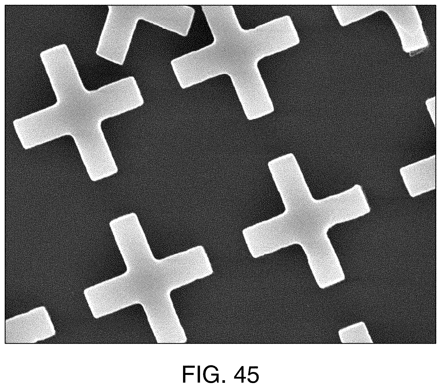
Description
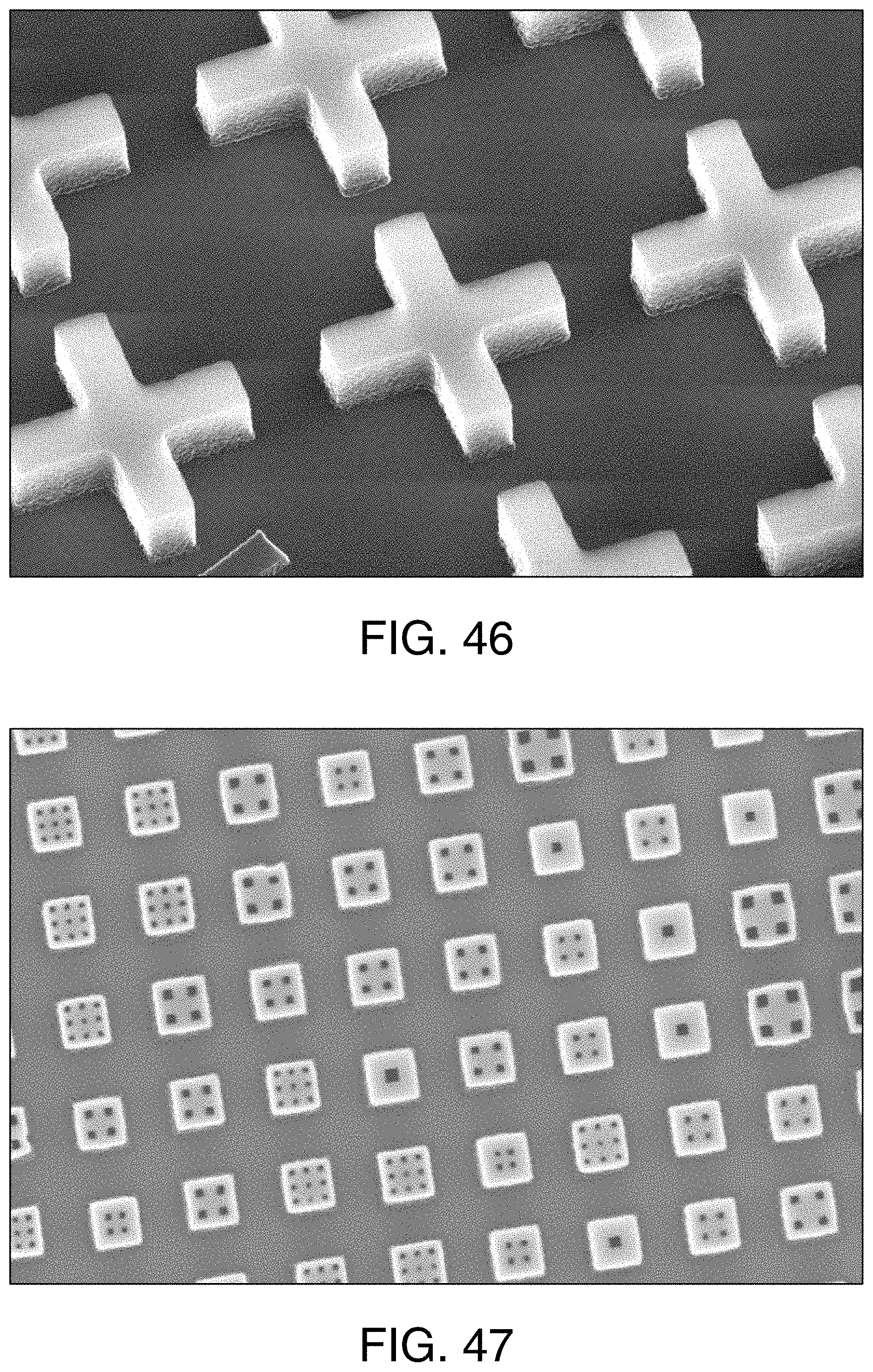
CROSS-REFERENCE TO RELATED APPLICATIONS
[0001] This application is a continuation of PCT/US2018/034460, filed on May 24, 2018, which claims priority to U.S. Provisional Application Ser. No. 62/510,670 filed on May 24, 2017, the contents of which are incorporated by reference herein and from which priority is claimed.
BACKGROUND
[0003] The replacement of bulk optical elements with diffractive planar components can solve certain weight and size constraints of optical devices. Certain optic devices suffer from large chromatic aberrations caused by lens dispersion. Metasurfaces can control optical wavefronts, and thus be used to realize flat metasurface lenses. Such lenses can reduce the size and complexity of certain imaging systems and realize new imaging modalities. Despite advances in metasurface fabrication techniques, certain optical devices made with metasurface lenses operate only at multiple or select wavelengths.
[0004] One challenge can be forming achromatic metalenses that produce the same focal length over a broad wavelength range. A second challenge can be forming broadband achromatic metalenses that work in the transmission mode for incident light waves with any arbitrary polarization state. Another challenge can be forming metalenses that can correct monochromatic aberrations, which cause degradation to imaging quality. There remains a need for improved techniques and systems for the metasurface lenses, which can correct both chromatic and monochromatic aberrations across a broad wavelength range, can control light with an arbitrary polarization state, and can work at either reflection or transmission mode.
SUMMARY
[0005] The disclosed subject matter provides techniques for creating a replacement for bulk optical elements with planar components based on metasurfaces.
[0006] In certain embodiments, a substantially flat optical component for lensing incoming electromagnetic radiation having at least one wavelength and a first phase profile into outgoing electromagnetic radiation having a second phase profile is provided. In certain examples, the optical components are made from a substrate and at least one metasurface. In certain examples, the optical components are made from several substrates and several metasurfaces. The metasurface can be made of a plurality of meta-units. Each meta-unit can be positioned at a distance that is less than the wavelength from at least a different optical meta-unit.
[0007] In accordance with some embodiments of the disclosed subject matter, each of the plurality of meta-units can have a certain shape to diffractively scatter the electromagnetic radiation. The plurality of meta-units can be configured to provide a range of optical phase and phase dispersion for a broadband achromatic metasurface lens.
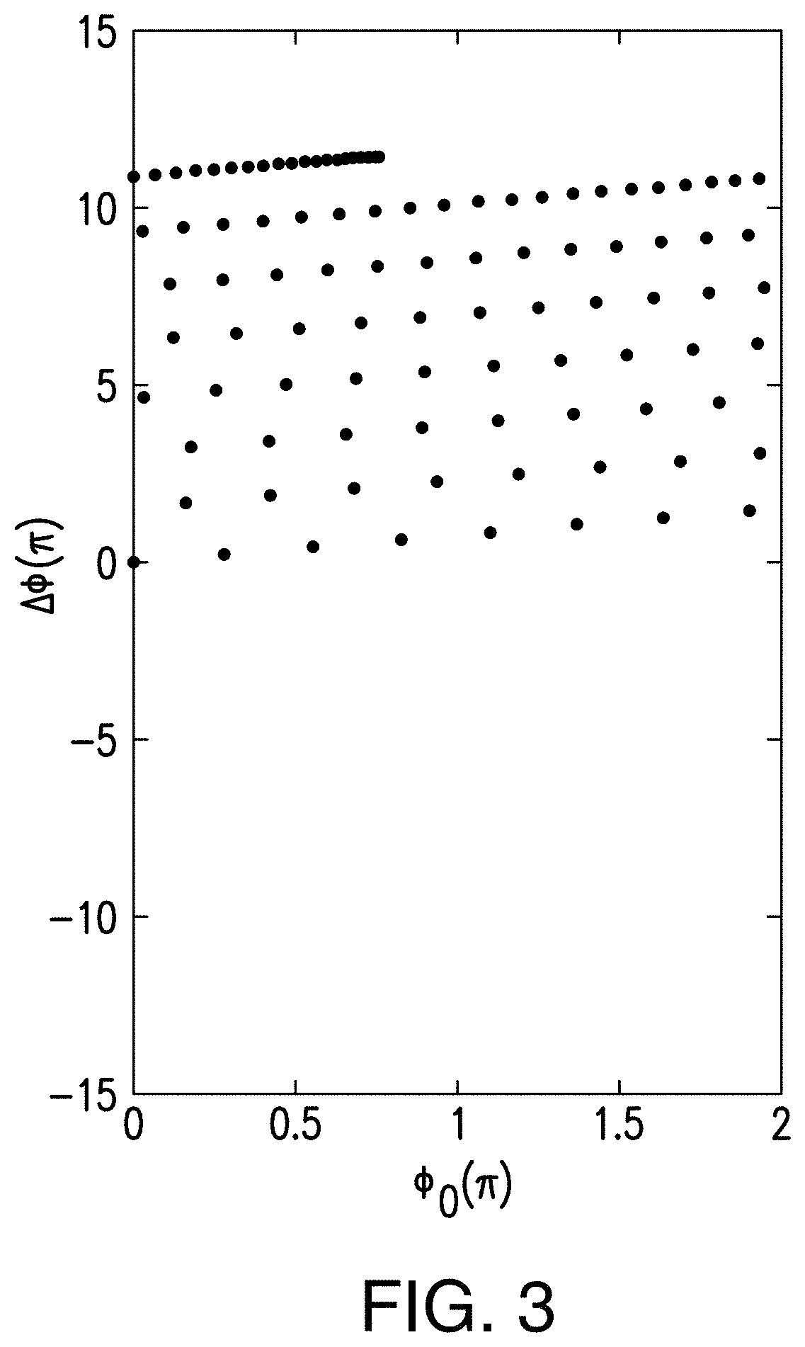
[0008] In certain embodiments, the plurality of meta-units can be made of a dielectric material. This dielectric material can be, for example, silicon, silicon nitride, gallium nitride, or titanium dioxide. In certain embodiments, the plurality of meta-units can be made of a metallic material. This metallic material can be, for example, aluminum, copper, silver, or gold.
[0009] In accordance with another embodiment of the disclosed subject matter, the metasurface is made of a patterned film layer. The film layer can be between 100 and 10,000 nm in thickness. The metasurface can be manufactured with machinery and techniques compatible with complementary metal oxide semiconductor (CMOS) fabrication facilities.
[0010] In accordance with embodiments of the disclosed subject matter, the meta-units can be partially or fully embedded in the substrate. The meta-units can vary in height. The meta-units can change shape along the height direction (for example, mushroom shaped).
[0011] The disclosed subject matter also provides fabrication methods for implementing the techniques described above. An example method of making a substantially flat optical component for lensing incoming electromagnetic radiation having at least one wavelength and a first phase profile into outgoing electromagnetic radiation having a second phase profile includes positioning a substrate and forming at least one metasurface on the substrate. Another example method of making a substantially flat optical component includes patterning several metasurfaces on several substrates and assembling them into a stack.
[0012] In some embodiments, the fabrication methods can include forming a substrate layer and a patterned film layer thereon having a thickness between 100 and 10,000 nm. The patterning can use electron-beam lithography, photolithography, deep ultra-violet lithography, or imprint lithography. The fabrication methods can also include partially or fully embedding the meta-units in the substrate.
BRIEF DESCRIPTION OF THE DRAWINGS
[0013] Further features and advantages of the present disclosure will become apparent from the following detailed description taken in conjunction with the accompanying figures showing illustrative embodiments of the present disclosure, in which:
[0014] FIG. 1A shows plots of the phase required for a converging lens, FIG. 1B shows plots of the phase required vs. wavelength at four locations labelled in (a), and FIG. 1C shows plots of typical phase vs. wavelength response of four dielectric meta-units.
[0015] FIG. 2 is a plot of phase dispersion profiles required for building achromatic metasurface lenses.
[0016] FIG. 3 is a plot showing Phase Offset and Phase Dispersion for creating a chromatic metasurface with focal length of 100 .mu.m, radius of 50 .mu.m, and operating wavelength range of 0.9-1.6 .mu.m.
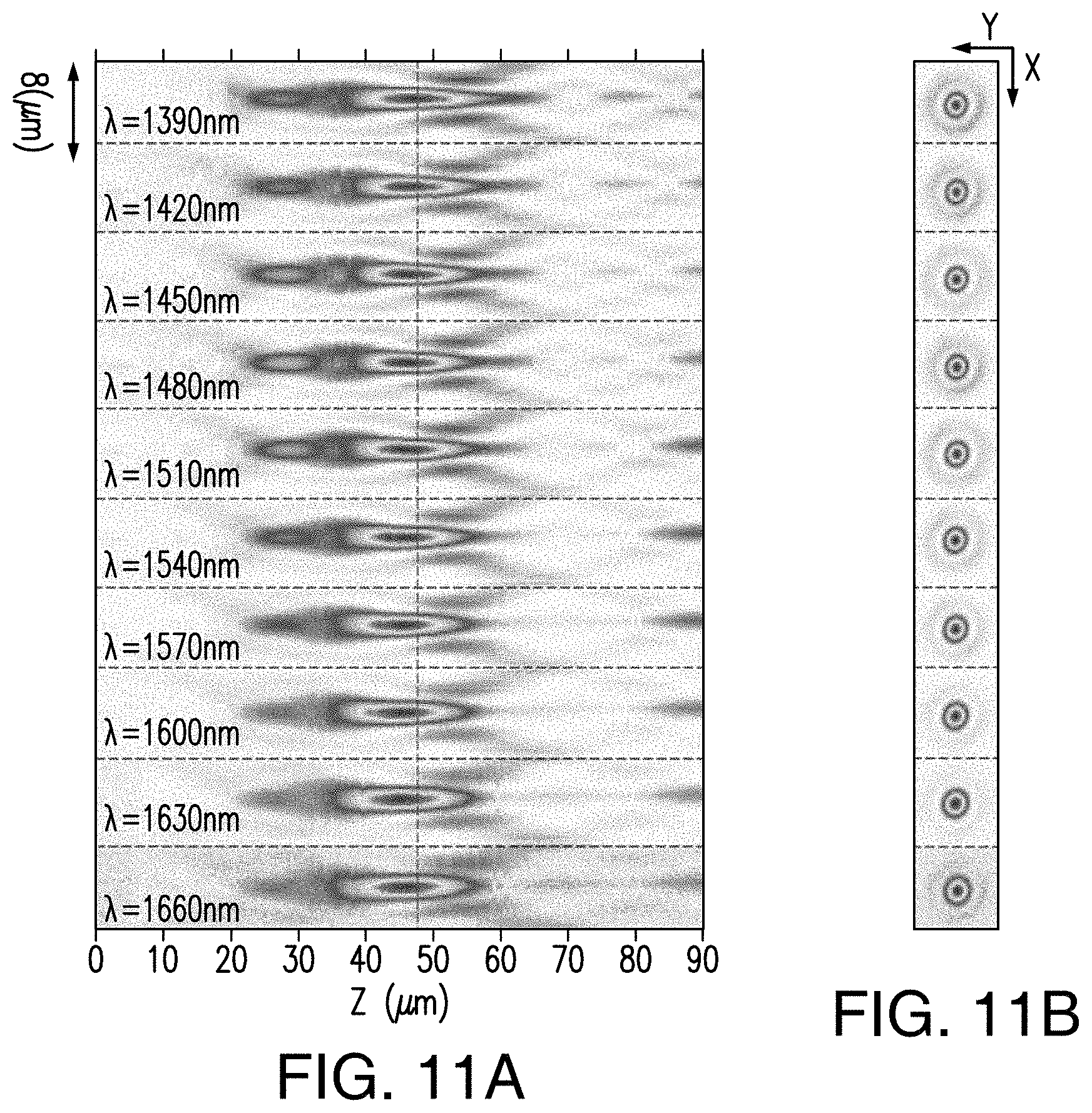
[0017] FIGS. 4A and 4B illustrate three example meta-unit libraries and the respective phase offset-dispersion space they can cover.
[0018] FIG. 5A is a diagram of a full-wave simulation showing the angular phase response of a sample meta-unit vs. wavelength. FIG. 5B is a diagram of a full-wave simulation showing the angular phase response of a sample meta-unit vs. wavelength. FIG. 5C is a diagram of a full-wave simulation showing the angular phase response of a sample meta-unit vs. wavelength. FIG. 5D is a diagram of a full-wave simulation showing the angular phase response of a sample meta-unit vs. wavelength.
[0019] FIGS. 6A and 6B show measured far-field intensity distributions of a focusing metasurface lens with a diameter of 100 .mu.m and numerical aperture (NA) of 0.24, where FIG. 6A is a plot of light intensity distributions on the longitudinal plane vs wavelength, and. FIG. 6B is a plot of light intensity distributions on the focal plane vs wavelength.
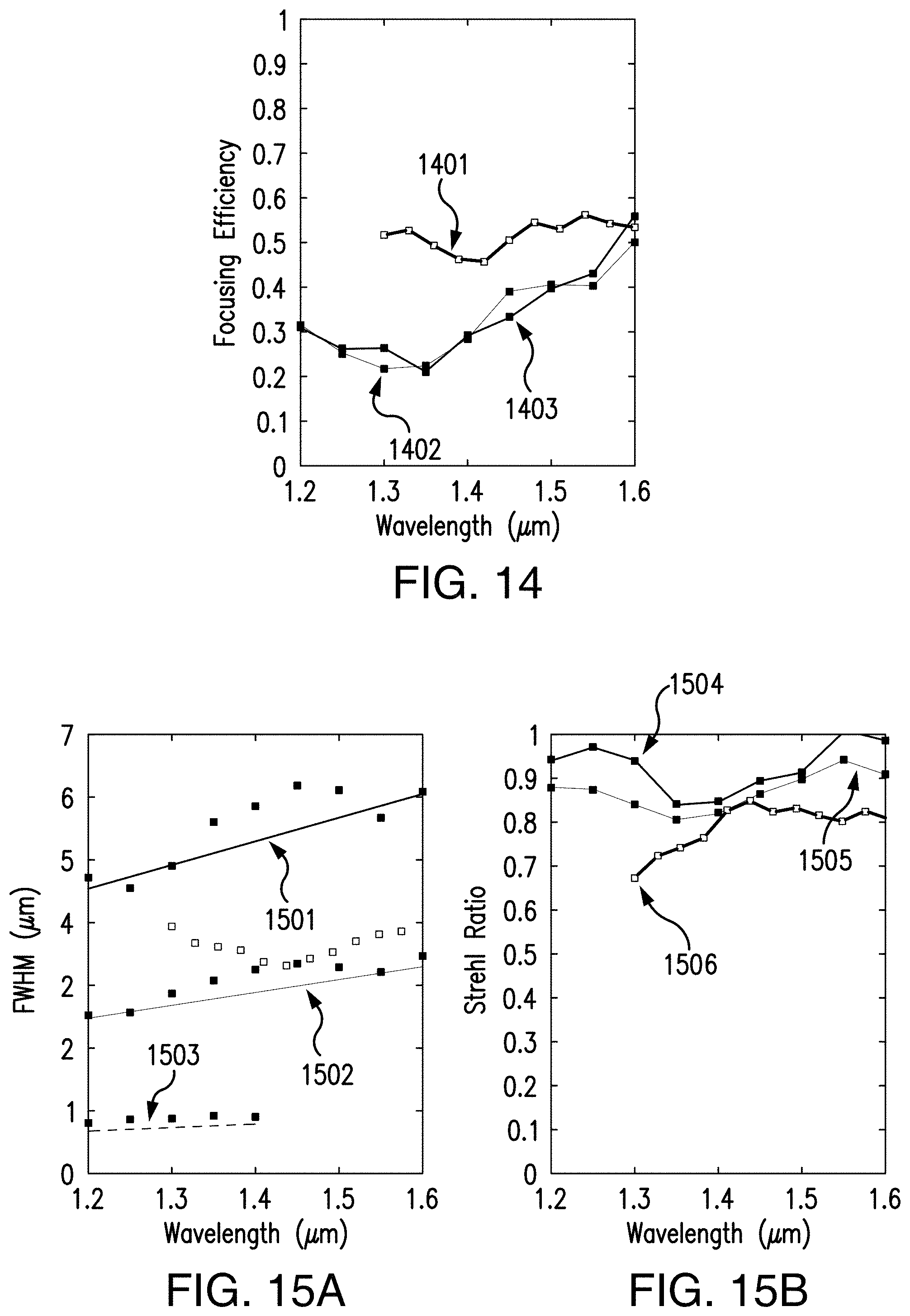
[0020] FIGS. 7A and 7B show measured far-field intensity distributions of a focusing metasurface lens with a diameter of 200 .mu.m and numerical aperture (NA) of 0.12, where FIG. 7A is a plot of light intensity distributions on the longitudinal plane vs wavelength, and FIG. 7B is a plot of light intensity distributions on the focal plane vs wavelength.
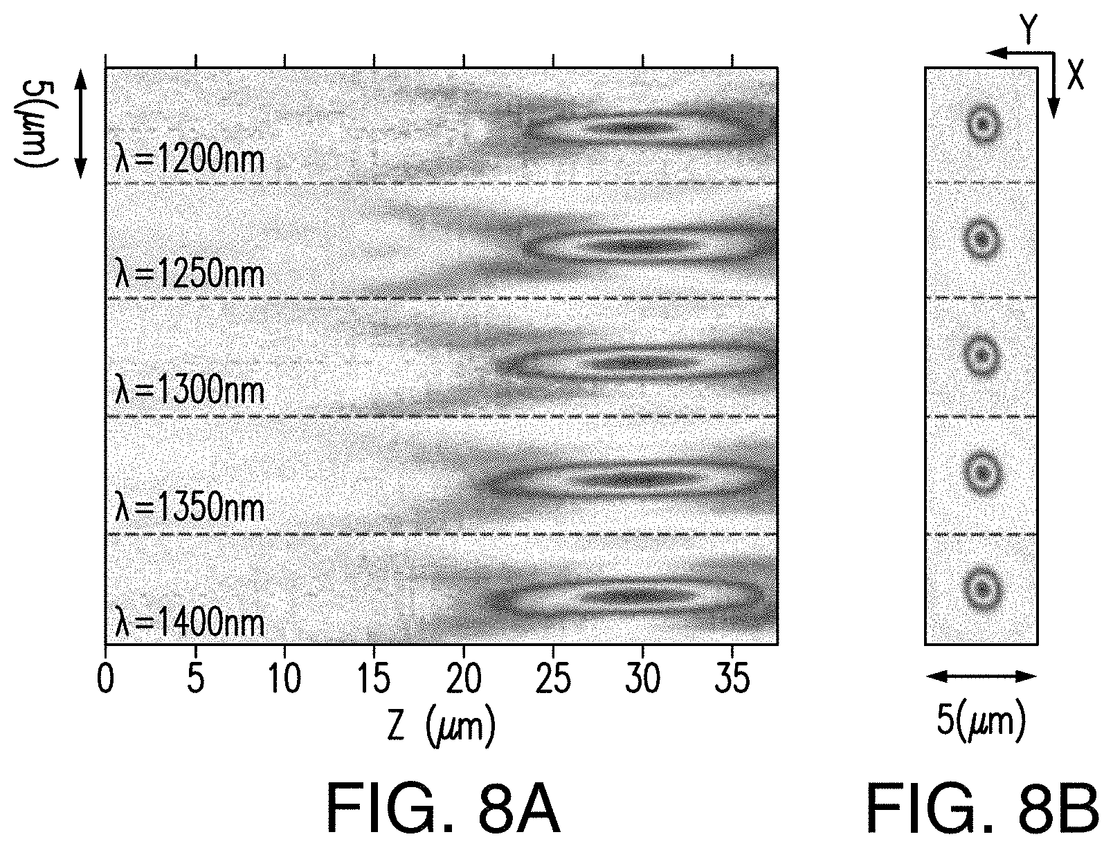
[0021] FIGS. 8A and 8B shows measured far-field intensity distributions of a focusing metasurface lens with a diameter of 100 .mu.m and numerical aperture (NA) of 0.85, where FIG. 8A is a plot of light intensity distributions on the longitudinal plane vs wavelength, and FIG. 8B is a plot of light intensity distributions on the focal plane vs wavelength.
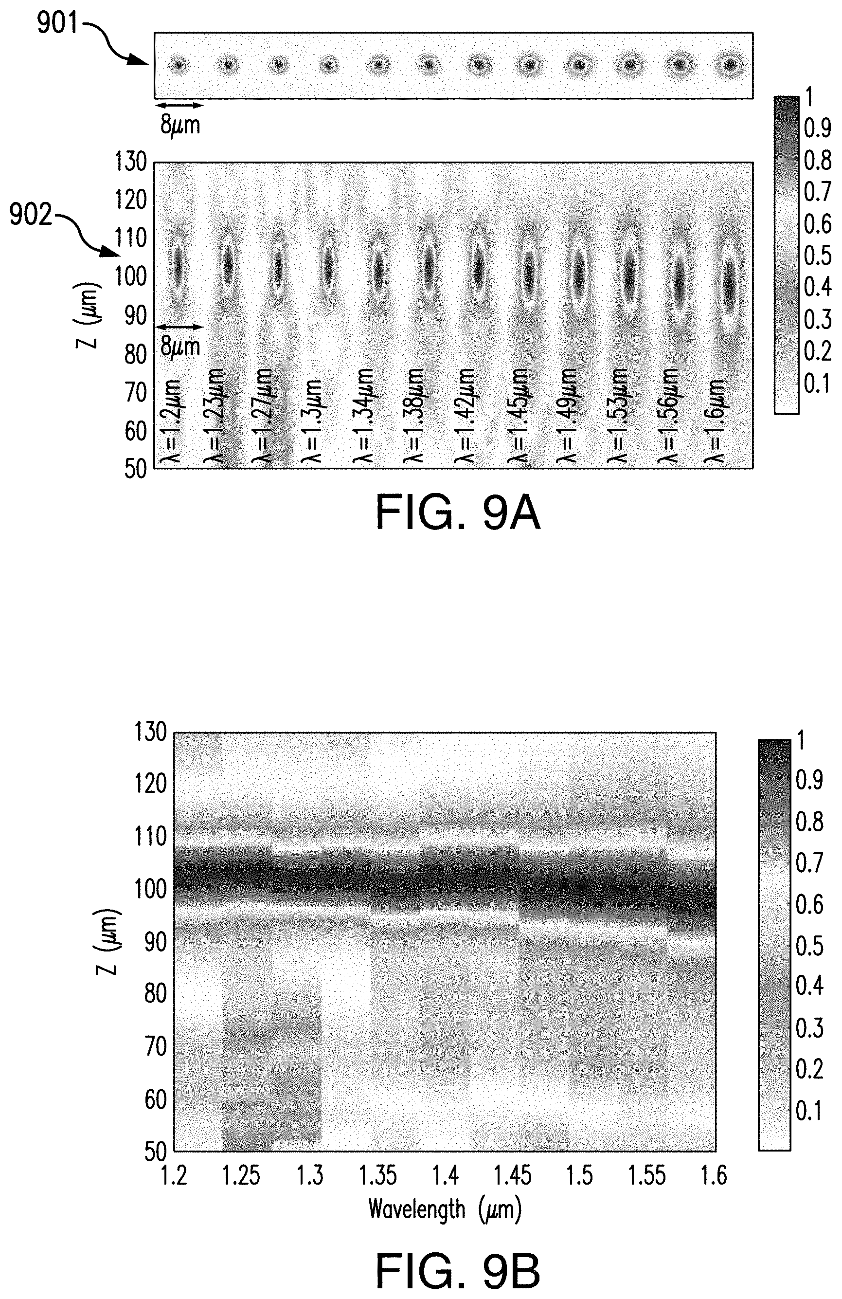
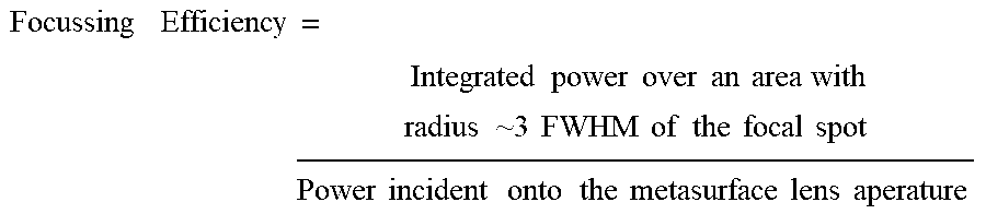
[0022] FIGS. 9A and 9B show simulated far-field intensity distribution of a focusing metasurface lens with a diameter of 100 .mu.m, focal distance of 100 .mu.m, and numerical aperture (NA) of 0.44 based on the 1400 nm tall meta-units, where FIG. 9A is a plot of light intensity distributions on the focal plane vs wavelength in the top panel, and a plot of light intensity distributions on the longitudinal plane vs wavelength in the bottom panel, and FIG. 9B shows s line scans of light intensity along the axis of the metasurface lens vs wavelength.
[0023] FIGS. 10A and 10B show simulated far-field intensity distribution of a focusing metasurface lens with a diameter of 100 .mu.m, focal distance of 20 .mu.m, and numerical aperture (NA) of 0.93 based on the 1400 nm tall meta-units, where FIG. 10A is a plot of light intensity distributions on the focal plane vs wavelength in the top panel and a plot of light intensity distributions on the longitudinal plane vs wavelength in the bottom panel, and FIG. 10B shows line scans of light intensity along the axis of the metasurface lens vs wavelength.
[0024] FIGS. 11A and 11B show measured far-field intensity distributions of a diverging metasurface lens with a diameter of 100 .mu.m, focal distance of 50 .mu.m, and numerical aperture (NA) of 0.7, where FIG. 11A is a plot of light intensity distributions on the longitudinal plane vs wavelength, and FIG. 11B is a plot of light intensity distributions on the focal plane vs wavelength.
[0025] FIG. 12A shows focal plane intensity distributions of a metasurface lens with diameter of 100 .mu.m and NA=0.24 at select wavelengths (Scale bar: 5 .mu.m), and FIG. 12B shows horizontal and vertical cuts (solid curves) across the corresponding measured focal spots in (a) compared with an ideal Airy spot (dashed curves).
[0026] FIG. 13 illustrates focal lengths as a function of wavelength for four experimentally demonstrated metasurface lenses.
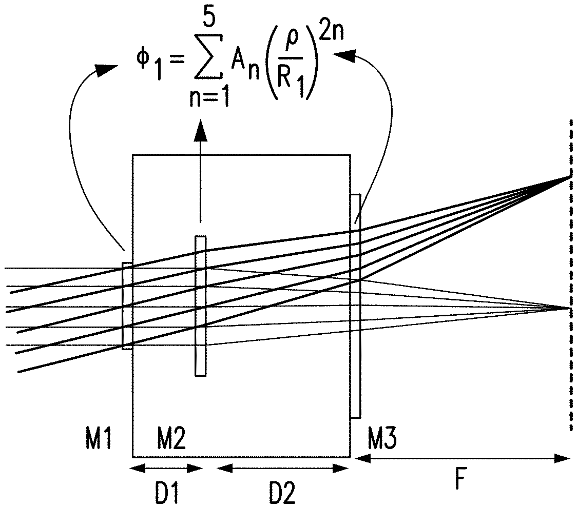
[0027] FIG. 14 shows measured focusing efficiencies of three experimentally demonstrated metalenses.
[0028] FIG. 15A shows extracted full-width at half-maximum (FWHM) of focal spots for four experimentally demonstrated metasurface lenses, and FIG. 15B shows calculated Strehl ratios for three experimentally demonstrated metasurface lenses.
[0029] FIGS. 16A-16D show optical and SEM images of an example fabricated metasurface lens working in the near-IR.
[0030] FIG. 17 is a SEM image of a small region of an example metasurface lens working in the near-IR.
[0031] FIG. 18 is a SEM image of a small region of an example metasurface lens working in the near-IR.
[0032] FIG. 19 is a SEM image of a small region of an example metasurface lens working in the near-IR.
[0033] FIG. 20 is a SEM image of a small region of an example metasurface lens working in the near-IR.
[0034] FIG. 21 is a SEM image of a small region of an example metasurface lens working in the near-IR.
[0035] FIG. 22 is a SEM image of a small region of an example a metasurface lens working in the near-IR.
[0036] FIG. 23 is a SEM image of a small region of an example metasurface lens working in the near-IR.
[0037] FIG. 24 is a SEM image of a small region of an example metasurface lens working in the near-IR.
[0038] FIG. 25 is a SEM image of a small region of an example metasurface lens working in the near-IR.
[0039] FIG. 26 is a SEM image of a small region of an example metasurface lens working in the near-IR.
[0040] FIG. 27 is an optical microscope image of an example chip with a number of amorphous-silicon near-IR metasurface lenses patterned on a quartz substrate.
[0041] FIG. 28 is an optical microscope image of an example near-IR metasurface lens patterned on a quartz substrate.
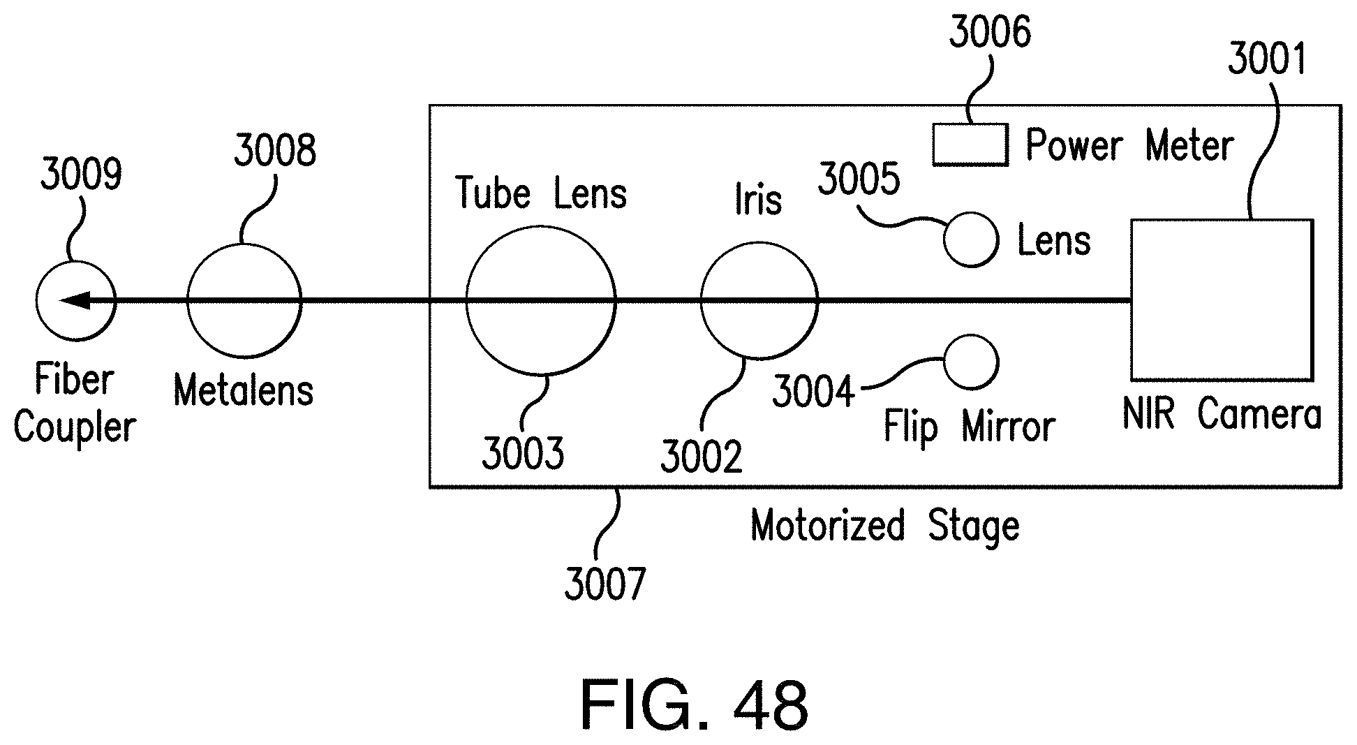
[0042] FIG. 29A illustrates an example technique for correcting chromatic and monochromatic aberrations in a metalens triplet consisting of three individual metalenses, and FIG. 29B shows an example metalens triplet.
[0043] FIGS. 30A-30C show ray-tracing results showing that the metalens triplet in FIG. 29 can correct both chromatic and monochromatic aberrations.
[0044] FIGS. 31A-31C are optical images of the elements of an example metalens triplet.
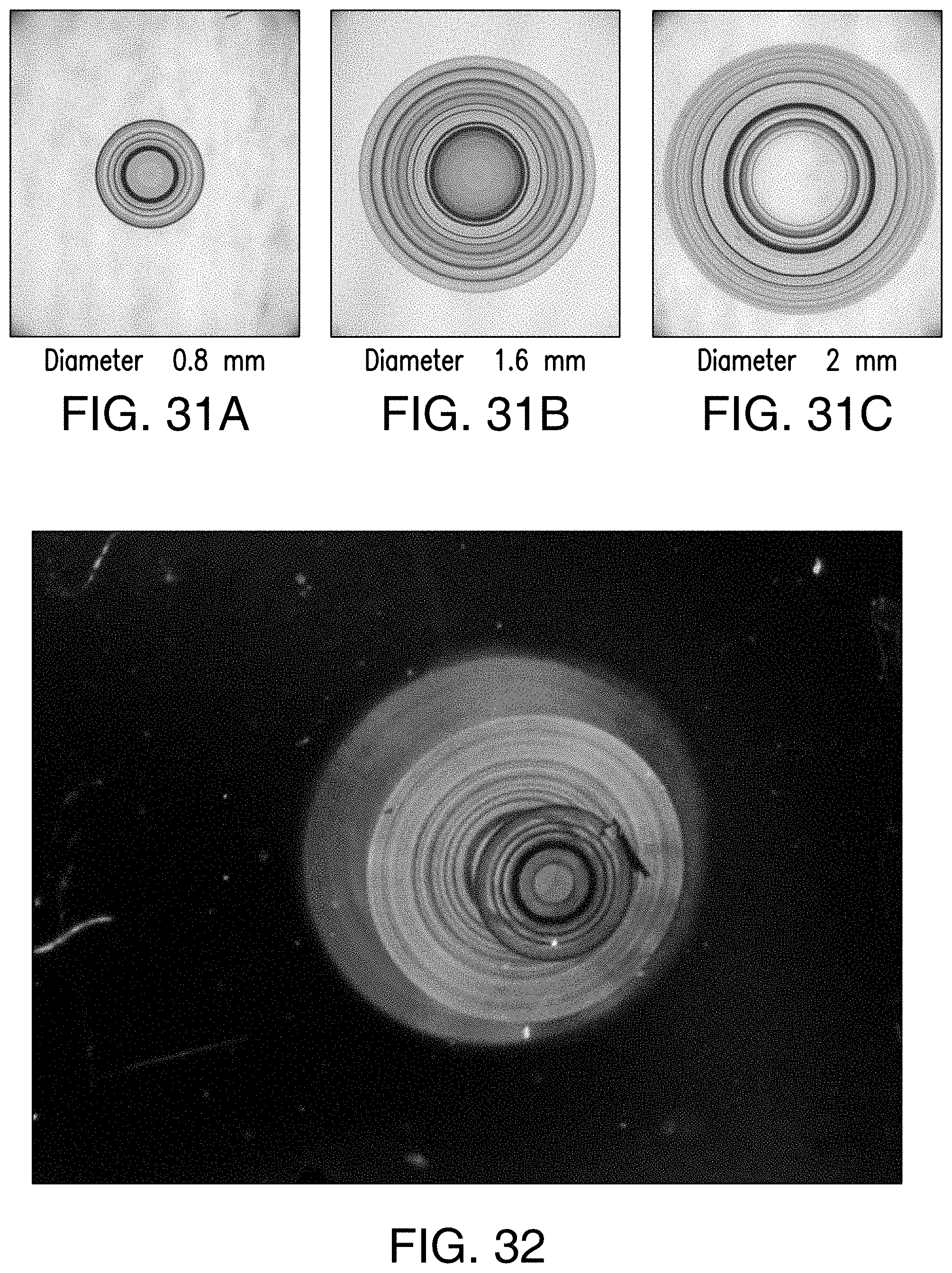
[0045] FIG. 32 is an example assembled metalens triplet used for imaging.
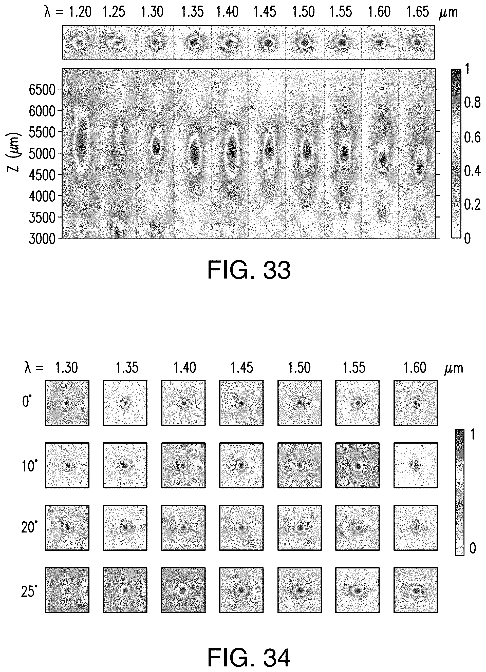
[0046] FIG. 33 shows measured far-field intensity distributions of the metalens triplet shown in FIG. 32, where (a) is a plot of light intensity distributions on the focal plane vs wavelength, and (b) is a plot of light intensity distributions on the longitudinal plane vs wavelength.
[0047] FIG. 34 shows measured intensity distributions on the focal plane at different wavelengths and a few incident angles for the metalens triplet shown in FIG. 32.
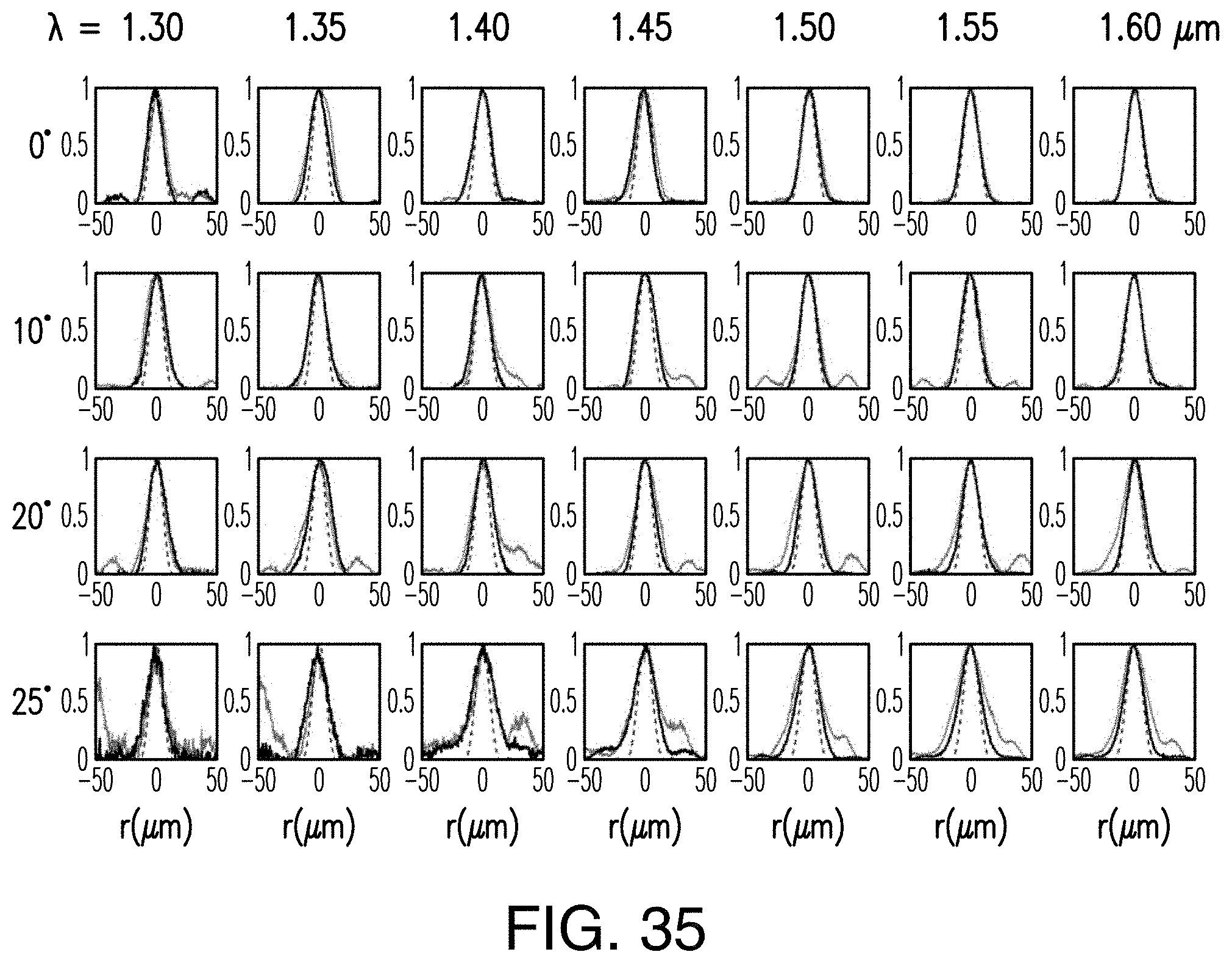
[0048] FIG. 35 shows line scans (solid curves) of measured intensity distributions shown in FIG. 34 compared with diffraction limited spots (dashed curves).
[0049] FIGS. 36A-36E show modulation transfer function (MTF) of an example metalens triplet.
[0050] FIGS. 37A-37C illustrate imaging of a USAF resolution target using an example metalens triplet under illumination sources with different bandwidths.
[0051] FIGS. 38A and 38B show imaging of the Siemens star and concentric ring with an example metalens triplet.
[0052] FIGS. 39A-39C show imaging reflection type objects illuminated with a broadband halogen lamp using an example metalens triplet.
[0053] FIG. 40 shows an example fabrication flow of amorphous silicon (a-Si) metasurface lenses.
[0054] FIG. 41 shows an example fabrication flow of TiO.sub.2 meta-units half-embedded in electron-beam resist PMMA.
[0055] FIG. 42 is an example fabrication flow of mushroom shaped meta-units for metasurface lenses.
[0056] FIG. 43 is an example fabrication flow of TiO.sub.2 meta-units with variable height in a single lithographic process.
[0057] FIG. 44 is an example fabrication flow of TiO.sub.2 meta-units using electron-beam sensitive TiO.sub.2 sol-gel.
[0058] FIG. 45 is a SEM image of example fabricated TiO.sub.2 meta-units based on direct electron-beam writing of TiO.sub.2 sol-gel.
[0059] FIG. 46 is a SEM image of example fabricated TiO.sub.2 meta-units based on direct electron-beam writing of TiO.sub.2 sol-gel.
[0060] FIG. 47 is a SEM image of example fabricated TiO.sub.2 meta-units based on direct electron-beam writing of TiO.sub.2 sol-gel.
[0061] FIG. 48 is a schematic depicting an example optical setup.
[0062] It is to be understood that both the foregoing general description and the following detailed description are exemplary and are intended to provide further explanation of the disclosed subject matter.
DETAILED DESCRIPTION
[0063] The systems and methods described herein provide for flat optical components to perform the function of a lens without chromatic aberration over a continuous and broad wavelength range and without monochromatic aberration over a certain range of incident angle of light. The disclosed subject matter can include a metasurface device. In some embodiments, the disclosed subject matter can have a thin, i.e., having a thickness near or smaller than the operating wavelengths, surface composed of optical nano-scatterers ("meta-units") spaced at subwavelength distances. In certain embodiment, shapes and placement of the disclosed subject matter can be designed to diffractively scatter incoming light into a desired output.
[0064] The disclosed subject matter can alter phase of the outgoing light waves. For example, a spatial profile of phase can be designed to perform a specific function, and the metasurfaces can be engineered to provide the phase required for that function. The meta-units can be made of dielectric materials, such as Silicon and Titanium Dioxide, which can have large refractive index but zero or low optical losses.
[0065] FIG. 1A provides plots of the phase required for a converging lens as a function of radial distance away from the center of the lens. Three wavelengths, shortest 101 (on top), intermediate 102 (in the middle), and longest 103 (on the bottom) are plotted for the free parameter C(.lamda.) given by the provided equations. The phase required at r.sub.0 can be zero for all wavelengths. FIG. 1B provides plots of the phase required vs wavelength at four locations (shown in FIG. 1A) along the radius of the lens. The highest curve 104 has the greatest phase dispersion, the second highest curve 105 has the second highest phase dispersion, the third highest curve 106 has the third highest phase dispersion, and the lowest curve 107 has the lowest phase dispersion. The dispersion profile for the positions #1-3 with this choice of free parameter C(.lamda.) can decrease as a function of increasing wavelength, which can match with the phase profiles provided by the meta-units (shown in FIG. 1C). The highest curve 108 has the greatest phase dispersion, the second highest curve 109 has the second highest phase dispersion, the third highest curve 110 has the third highest phase dispersion, and the lowest curve 111 has the lowest phase dispersion. The phase profile required for broadband metasurface lenses is given by the equation
.phi. ( r , .lamda. ) = - 2 .pi. .lamda. f 2 + r 2 + C ( .lamda. ) ( 3 ) where C ( .lamda. ) = 2 .pi. .lamda. f 2 + ( r 0 ) 2 ( 4 ) ##EQU00001##
[0066] In some embodiments, a degree of freedom C(.lamda.) within the governing equation for a metasurface lens (its optical phase profile) can be modified so the required phase dispersion according to the governing equation can match with the phase dispersion naturally achievable by the meta-units. In some embodiments, an error minimization including both choice of meta-units and choice of governing equation can be carried out to reduce both amplitude and phase mismatch between the ideal and the achievable metasurface lenses. For example, the error between the meta-units achievable and the metasurface lens governing equation chosen can be reduced or minimized by allowing variable choice between both meta-units and governing equation.
[0067] FIG. 2 illustrates a plot of phase dispersion profiles 200 at four locations along the radius of an exemplary achromatic metasurface lens. The highest curve 201 has the greatest phase dispersion, the second highest curve 202 has the second highest phase dispersion, the third highest curve 203 has the third highest phase dispersion, and the lowest curve 204 has the lowest phase dispersion. The linear profiles can be parametrized by a Phase Offset term (.PHI..sub.0) and the slope
( d .phi. d .omega. ) , ##EQU00002##
which represents the Phase Dispersion term.
[0068] FIG. 3, for the purpose of illustration and not limitation, provides a plot of phase offset-dispersion requirement space (represented by the area covered by dots) for a metasurface lens with focal length of 100 .mu.m and radius of 50 .mu.m with numerical aperture (NA) 0.44. The phase-offset can be wrapped over 0-2n interval. The free parameter C(.omega.) is given by the given equation with r.sub.0=50 .mu.m.
.phi. ( r , .lamda. ) = - 2 .pi. .lamda. f 2 + r 2 + C ( .lamda. ) ( 5 ) where C ( .lamda. ) = 2 .pi. .lamda. f 2 + ( r 0 ) 2 ( 6 ) where r 0 = 50 m ( 7 ) ##EQU00003##
[0069] FIG. 4A shows three meta-unit libraries and the phase offset-dispersion space they can cover. Each library contains a few meta-unit archetypes, each representing a sub-class of meta-units composed of the archetype's basic shape but with varying in-plane geometrical parameters. The meta-units are assumed to be made of amorphous silicon and patterned on a quartz substrate. In the phase offset-dispersion space, x-axis is phase of the lowest frequency (or largest wavelength, .lamda.=1.6 .mu.m), and y-axis is phase dispersion, .DELTA..PHI.=d.PHI./d.omega..times..DELTA..omega., for the chosen bandwidth .DELTA..omega. (i.e., .lamda.=1.2-1.6 .mu.m). Meta-unit library 1 contains singular pillars, annular pillars, and concentric rings. The meta-units' height is 800 nm. Note the great expanse of coverage of the phase-dispersion space compared to only employing the conventional choice of singular pillars. Meta-unit library 2 has the same three meta-unit archetypes as meta-unit library 1 but the height of the meta-units is increased to 1,400 nm. The range of dispersion achieved is nearly doubled. Meta-unit library 3 keeps the same height as Meta-unit library 2 but switches to archetypes with four-fold symmetry instead of rotational symmetry. This switch expands the number of archetypes to include crosses and inscribed crosses. The coverage of the phase phase-dispersion space is further improved. FIG. 4B shows five exemplary meta-units with very different optical phase dispersion. The meta-units are effectively truncated waveguides. The first meta-unit shown in the first row of FIG. 4B is the most dispersive type of meta-units: the shorted wavelength has very good overlap with the meta-unit, which is a rod with intermediate radius, whereas the longest wavelength does not have as good an overlap. This creates a very dispersive phase response. The last meta-unit shown in the fifth row of FIG. 4B is the least dispersion type of meta-units: all the wavelengths have similar modal overlap with the meta-unit cross-section, which is a small annular ring.
[0070] The disclosed subject matter can introduce a range of novel meta-unit structures and can utilize them to provide the phase dispersion required for broadband functionality. In some embodiments, the meta-units can be distal from the center of the metasurface lens and contribute to the focal spot at large angles.
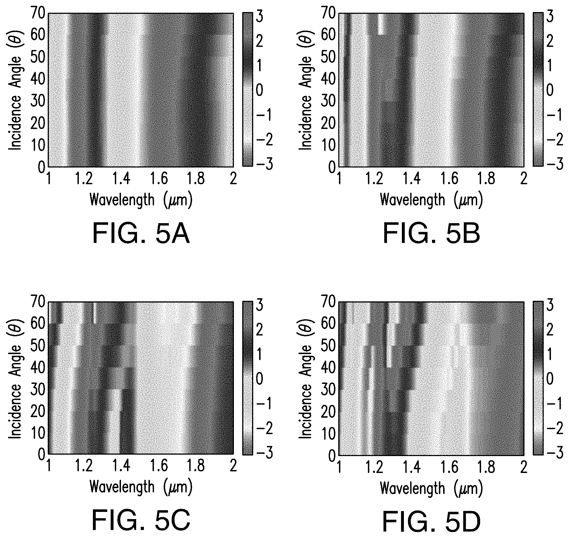
[0071] FIGS. 5A-5D show angular phase response of a few exemplary meta-units. The meta-units can be excited by plane waves at a direction normal to the surface of the substrate. The phase of forward scattered light can be monitored at a half circle centered at the meta-unit, and the radius of the circle can be many times the wavelength (far-field regime). Different observation angles can be indicated by .theta.. Each angular response diagram shows that the wavefronts of light scattered by the meta-units are not spherical in shape: the phase response along the substrate normal direction (.theta.=0) can be different from the phase response along .theta.=45-degree direction. Meta-units could be chosen according to their locations on a metasurface lens and their angular phase response.
[0072] The disclosed subject matter can include a multi-angle metasurface. The multi-angle metasurface can have different metasurface responses for different angles of incident. In some embodiments, the disclosed subject matter can be utilized to remove focal plane aberrations, to concentrate solar rays to one spot or to capture all incident angles of a small footprint on-chip detector.
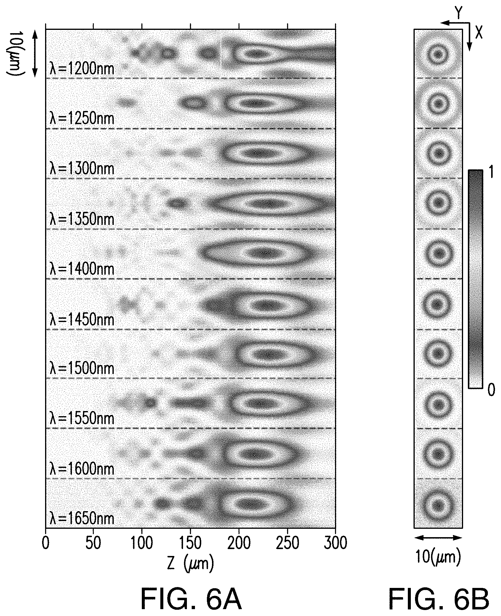
[0073] FIGS. 6A-6B, for the purpose of illustration and not limitation, show measured far-field intensity distributions of a focusing metasurface lens with a diameter of 100 .mu.m and numerical aperture (NA) of 0.24. FIG. 6A shows measured light intensity distributions on the longitudinal plane, showing achromatic focusing over a wide range of wavelengths. FIG. 6B shows measured light intensity distributions on the focal plane, showing that diffraction limited focal spots are obtained over a wide range of wavelengths.
[0074] FIGS. 7A-7B show measured far-field intensity distributions of a focusing metasurface lens with a diameter of 200 .mu.m and numerical aperture (NA) of 0.12. FIG. 7A shows measured light intensity distributions on the longitudinal plane, showing achromatic focusing over a wide range of wavelengths. FIG. 7B shows measured light intensity distributions on the focal plane, showing that diffraction limited focal spots are obtained over a wide range of wavelengths.
[0075] FIGS. 8A-8B show measured far-field intensity distributions of a focusing metasurface lens with a diameter of 100 .mu.m and numerical aperture (NA) of 0.85. FIG. 8A shows measured light intensity distributions on the longitudinal plane, showing achromatic focusing over a wavelength range of .lamda.=1,200-1,400 nm. FIG. 8B shows measured light intensity distributions on the focal plane, showing that diffraction limited focal spots are obtained over a wavelength range of .lamda.=1,200-1,400 nm.
[0076] FIGS. 9A-9B show simulated far-field intensity distribution of a focusing metasurface lens with a diameter of 100 .mu.m, focal distance of 100 .mu.m, and numerical aperture (NA) of 0.44 based on the 1400 nm tall meta-units. The simulation is conducted with finite-difference time-domain techniques. Top panel of FIG. 9A shows simulated light intensity distributions on the focal plane, showing that diffraction limited focal spots are obtained over a wide range of wavelengths. Bottom panel of FIG. 9A shows simulated light intensity distributions on the longitudinal plane, showing achromatic focusing over a wide range of wavelengths. FIG. 9B shows line scans of light intensity along the axis of the metasurface lens, showing achromatic focusing over a wide range of wavelengths.
[0077] FIGS. 10A and 10B show simulated far-field intensity distribution of a focusing metasurface lens with a diameter of 100 .mu.m, focal distance of 20 .mu.m, and numerical aperture (NA) of 0.93 based on the 1400 nm tall meta-units. Top panel of FIG. 10A shows simulated light intensity distributions on the focal plane, showing that diffraction limited focal spots are obtained over a wide range of wavelengths. Bottom panel of FIG. 10A shows simulated light intensity distributions on the longitudinal plane, showing achromatic focusing over a wide range of wavelengths. FIG. 10B shows line scans of light intensity along the axis of the metasurface lens, showing achromatic focusing over a wide range of wavelengths.
[0078] FIGS. 11A and 11B show measured far-field intensity distributions of a diverging metasurface lens with a diameter of 100 .mu.m, focal distance of 50 .mu.m, and numerical aperture (NA) of 0.7. Measured focal spots are virtual spots behind the metasurface, where the wavefront originates. FIG. 11A shows measured light intensity distributions on the longitudinal plane, showing achromatic performance over a wide range of wavelengths. FIG. 11B shows measured light intensity distributions on the focal plane, showing that diffraction limited virtual focal spots are obtained over a wide range of wavelengths.
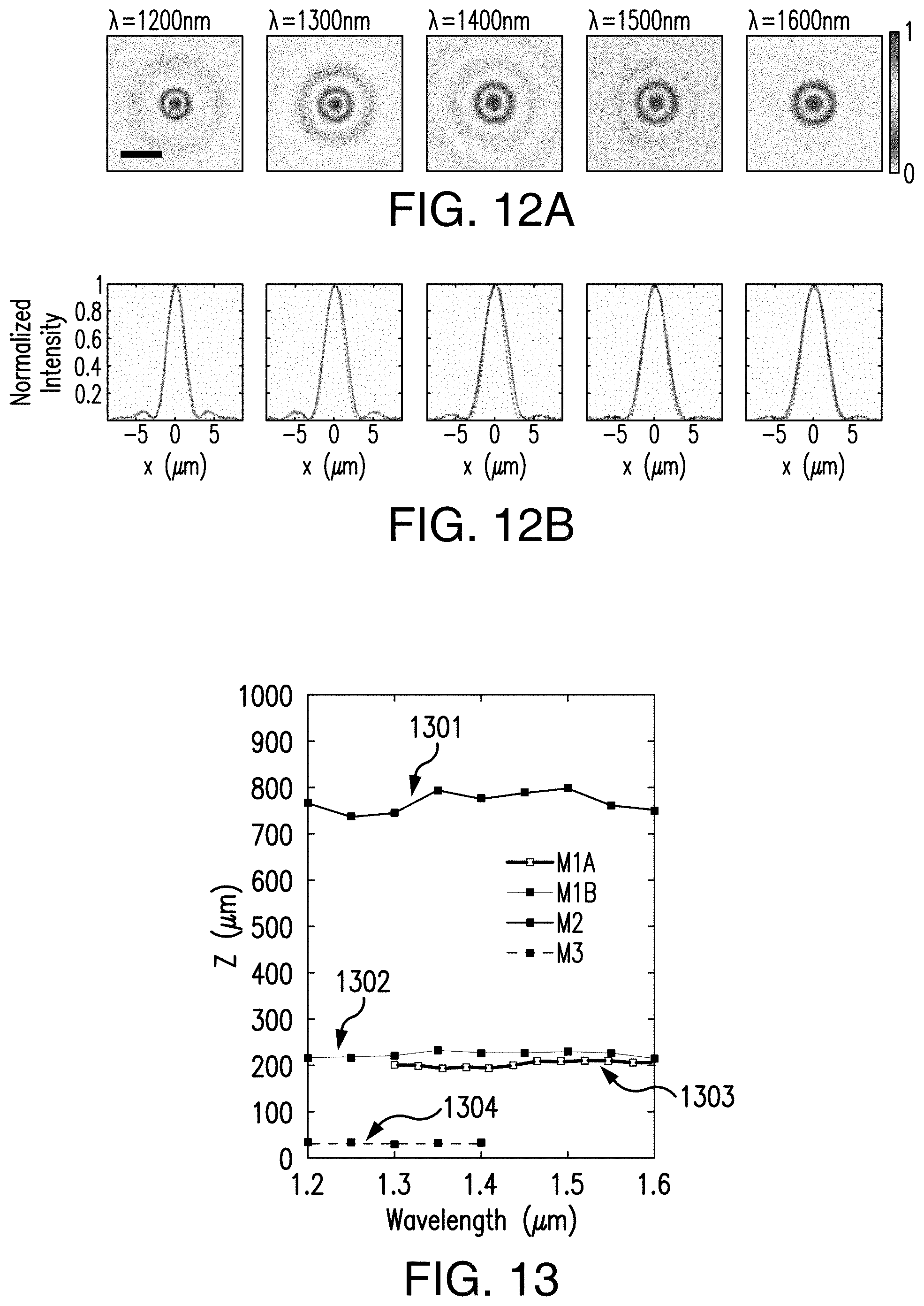
[0079] FIG. 12A shows measured focal plane intensity distributions of a metasurface lens with diameter of 100 .mu.m and NA=0.24 at select wavelengths. FIG. 12B shows horizontal and vertical cuts across the measured focal spots in FIG. 12A compared with an ideal Airy spot, showing that the focal spots are diffraction limited.
[0080] FIG. 13 shows measured focal distances as a function of wavelength for four experimentally demonstrated metasurface lenses, showing that the maximum shift from the mean focal length is limited to 2-5% for the entire design bandwidth and indicating that the metasurface lenses are able to correct chromatic aberration. The first plot 1301 has the greatest Z value, the second plot 1302 has the second greatest Z value, the third plot 1303 has the third greatest Z value, and the fourth plot 1304 has the lowest Z value.
[0081] FIG. 14 shows measured focusing efficiencies of three experimentally demonstrated metalenses. The first plot 1401 has the greatest focusing efficiency, the second plot 1402 has the second greatest peak focusing efficiency, and the third plot 1403 has the lowest peak focusing efficiency. In some embodiments, transmission and focusing efficiencies can be quantified. The transmission efficiency of metasurface lenses can be defined as
Transmission = Power transmitted through the metasurface lens aperature Power incident onto the metasurface lens aperature ##EQU00004##
[0082] Thus, determining transmission efficiency involves measuring optical power transmitted through the area of a metasurface lens (i.e., quartz substrate covered by silicon metasurface structures) and optical power transmitted through just the quartz substrate of the same area as the metasurface lens.
[0083] In some embodiments, the focusing efficiency of metasurface lenses can be defined as:
Focussing Efficiency = Integrated power over an area with radius ~ 3 FWHM of the focal spot Power incident onto the metasurface lens aperature ##EQU00005##
[0084] Thus, determining focusing efficiency involves measuring optical power that is concentrated onto a circular aperture on the focal plane that has a diameter approximately three times the FWHM of the focal spot and optical power transmitted through the area of a metasurface lens.
[0085] FIG. 15A is extracted full-width at half-maximum (FWHM) of focal spots for four experimentally demonstrated metasurface lenses. Straight lines represent theoretical FWHM. FIG. 15A contains three plots. The first plot 1501 has the greatest FWHM value, the second plot 1502 has the second greatest FWHM value, and the third plot 1503 has the third greatest FWHM value. FIG. 15B contains three plots. The first plot 1504 has the greatest Strehl ratio, the second plot 1505 has the second greatest Strehl ratio, and the third plot 1506 has the third greatest Strehl ratio. FIG. 15B shows calculated Strehl ratios for three experimentally demonstrated metasurface lenses. The values are around or above 0.8 for all wavelengths, satisfying the condition for diffraction limited focal spots.
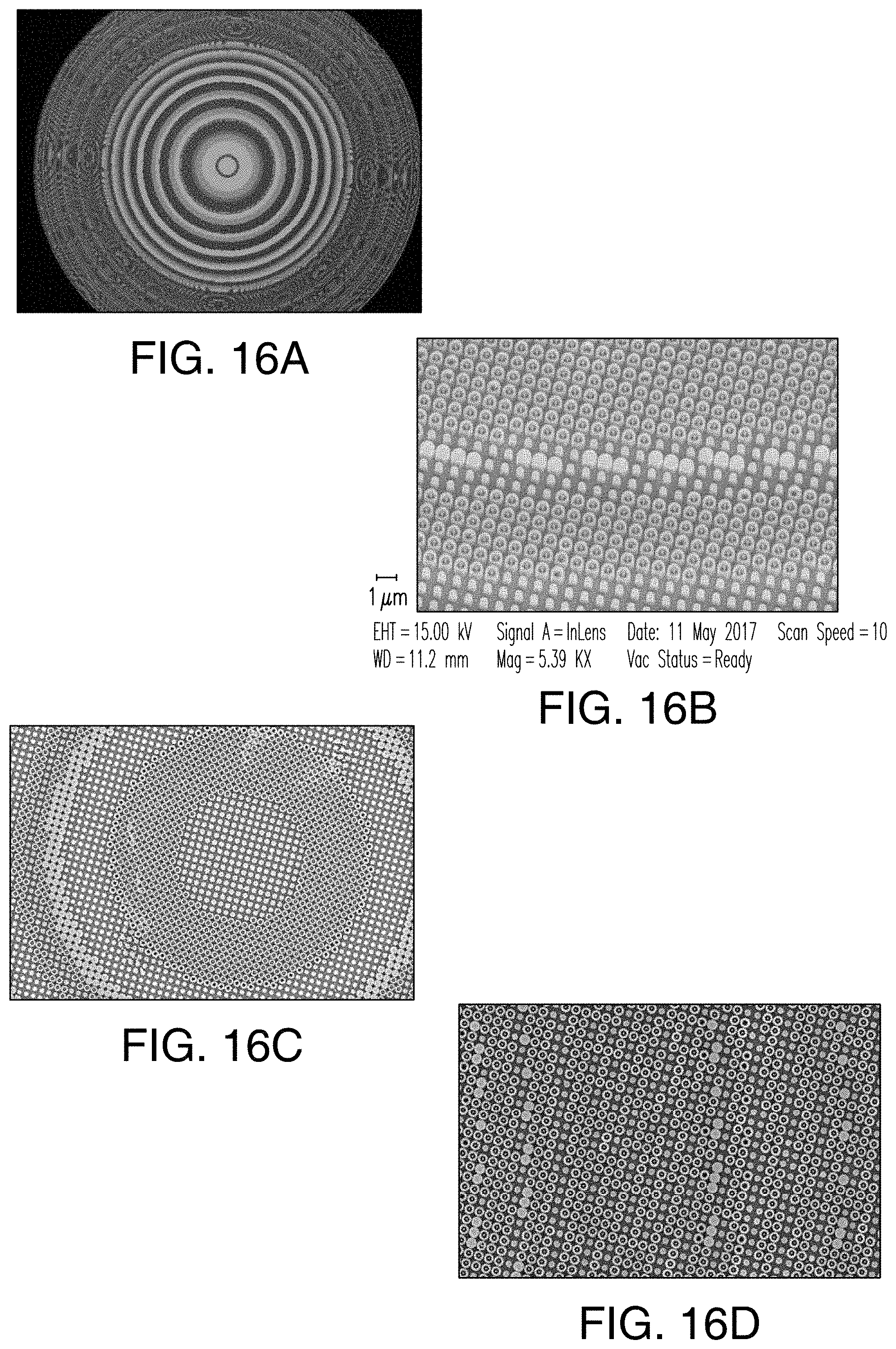
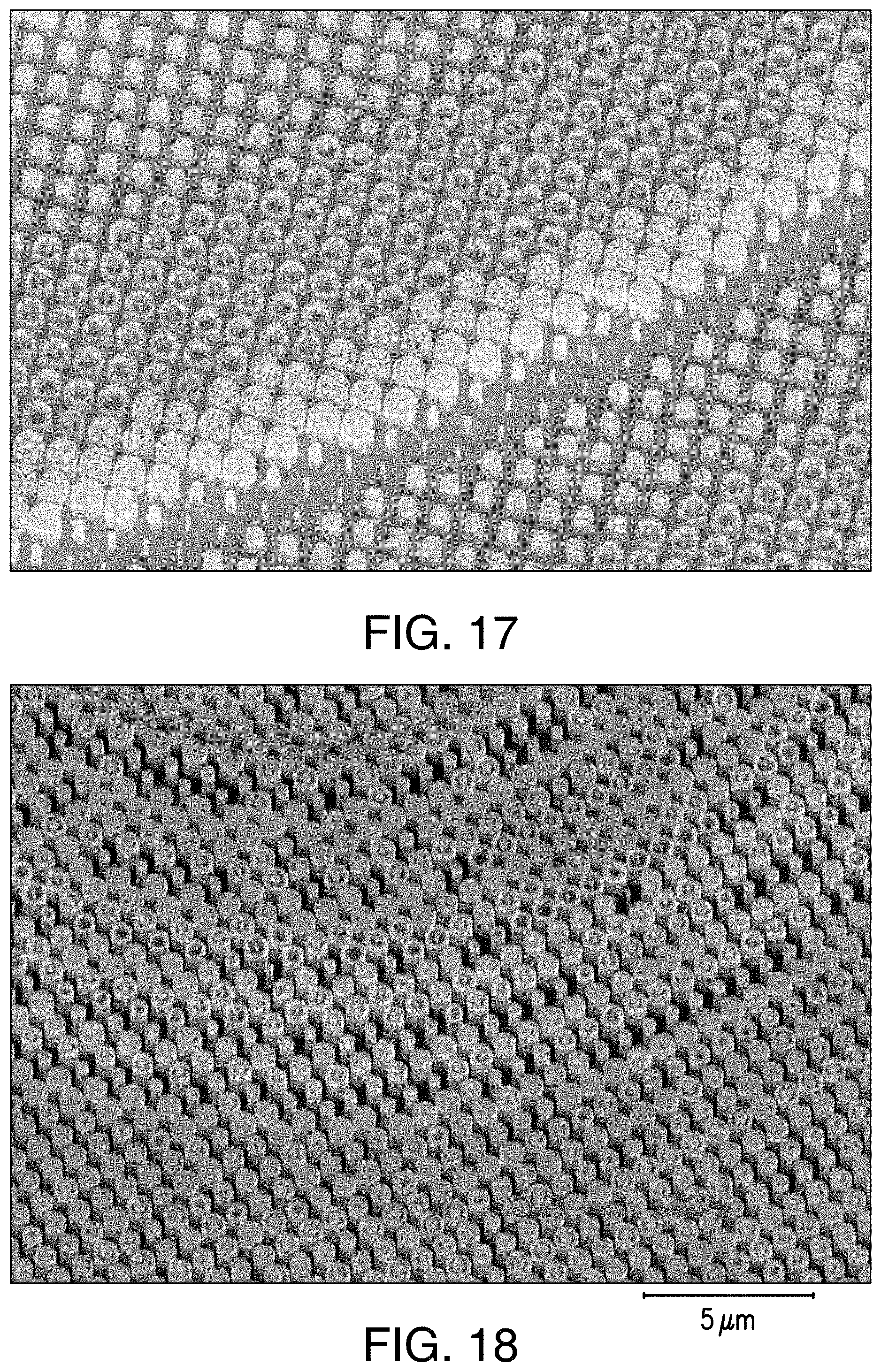
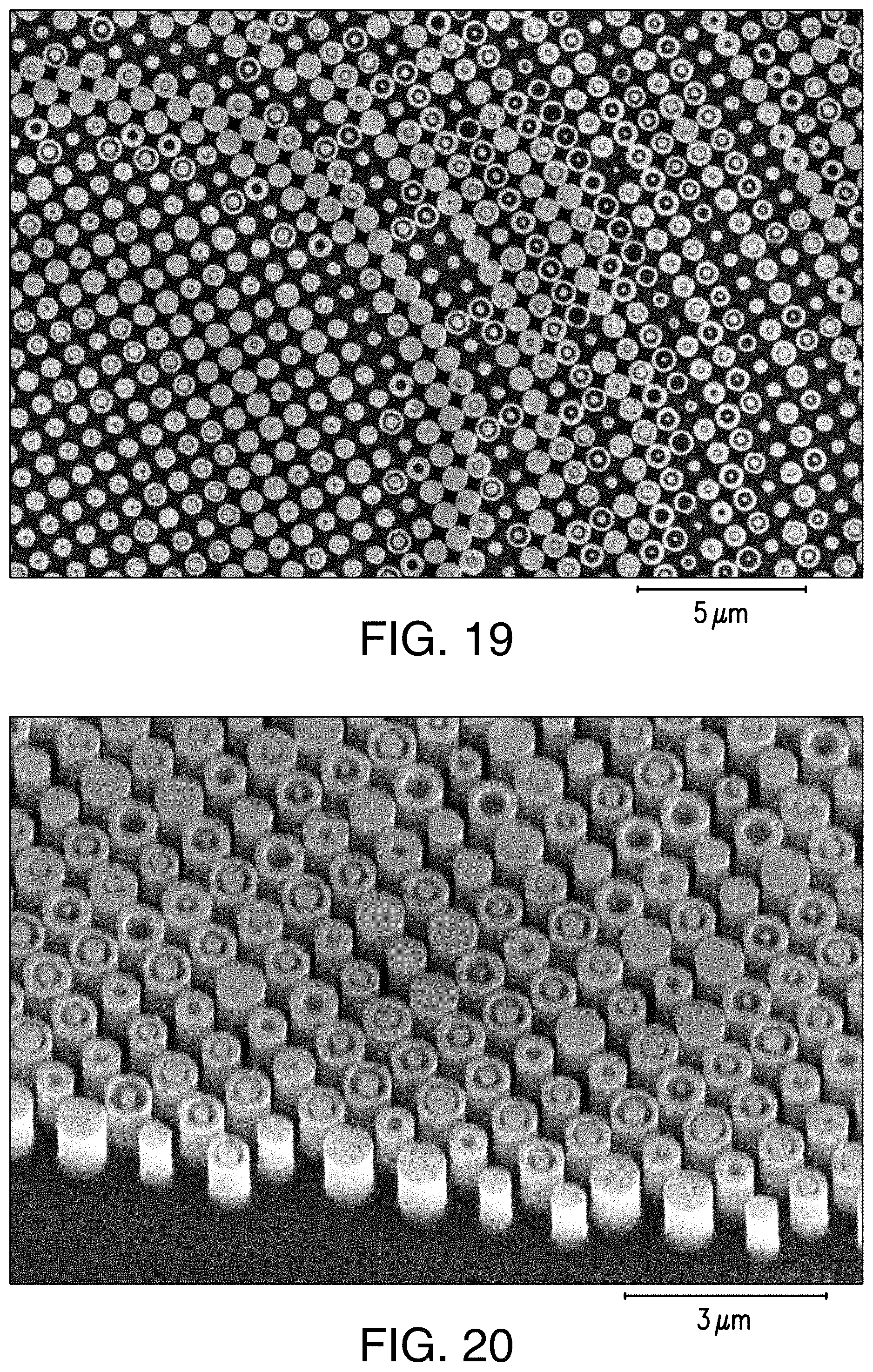
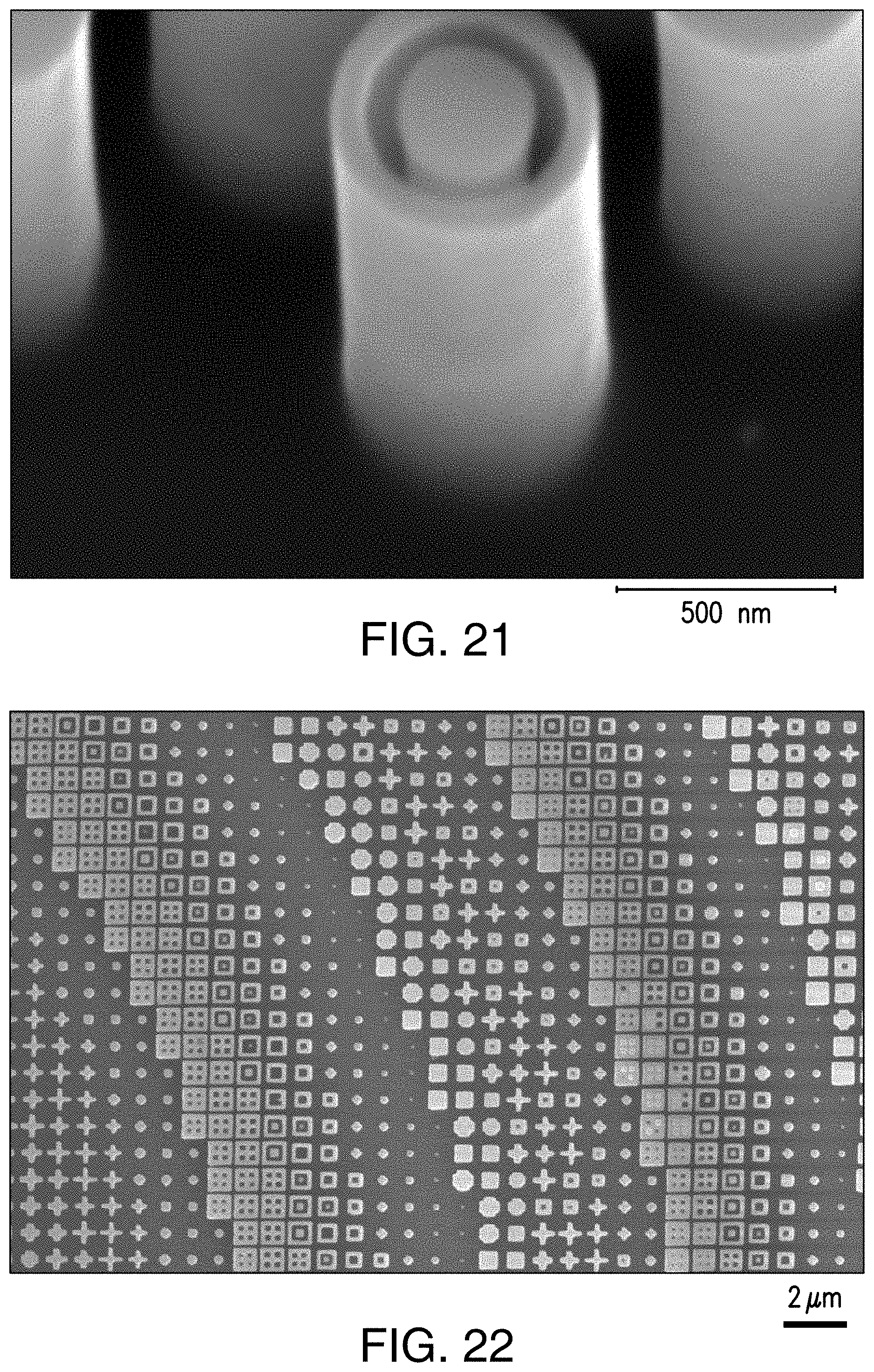
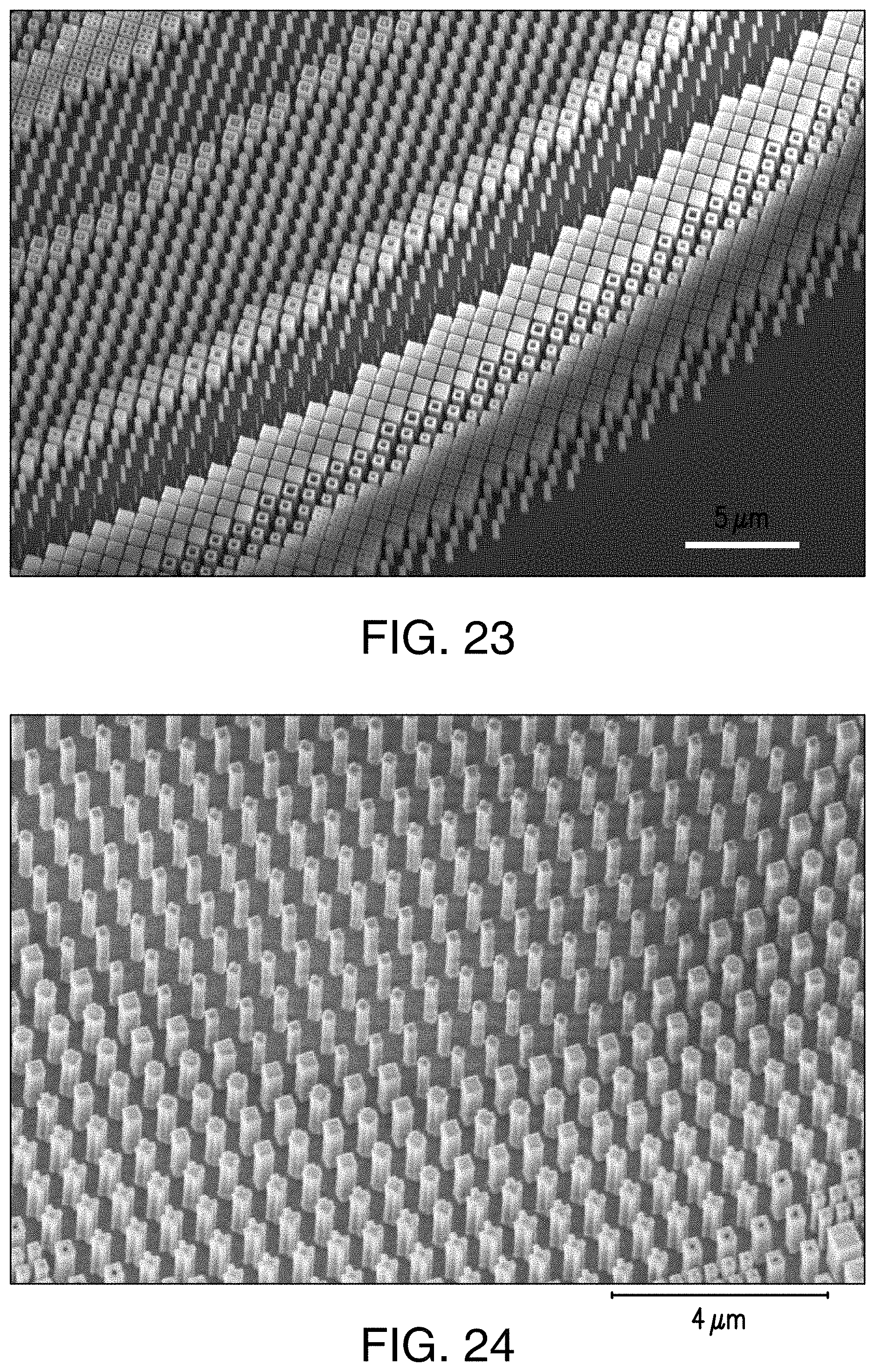
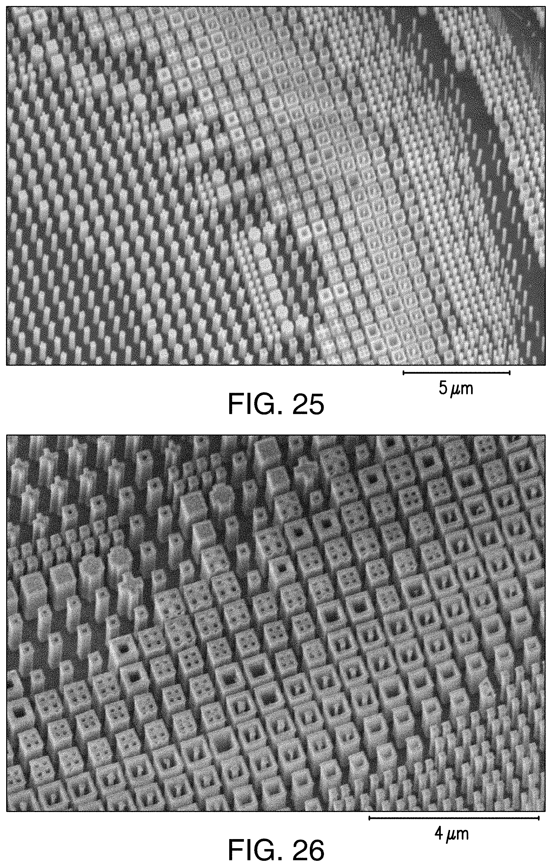
[0086] FIG. 16A is an optical image of an example fabricated metasurface lens working in the near-IR. FIGS. 16B-16D are scanning electron microscope (SEM) images of regions of an example metasurface lens working in the near-IR. FIG. 17 is an SEM image of a region of an example metasurface lens working in the near-IR. FIGS. 18-21 are SEM images of regions of an example metasurface lens working in the near-IR. FIGS. 22 and 23 are SEM images of regions of an example metasurface lens working in the near-IR. FIGS. 24-26 are SEM images of regions of an example metasurface lens working in the near-IR. All these exemplary metasurface lenses are made of amorphous silicon patterned on quartz substrates.
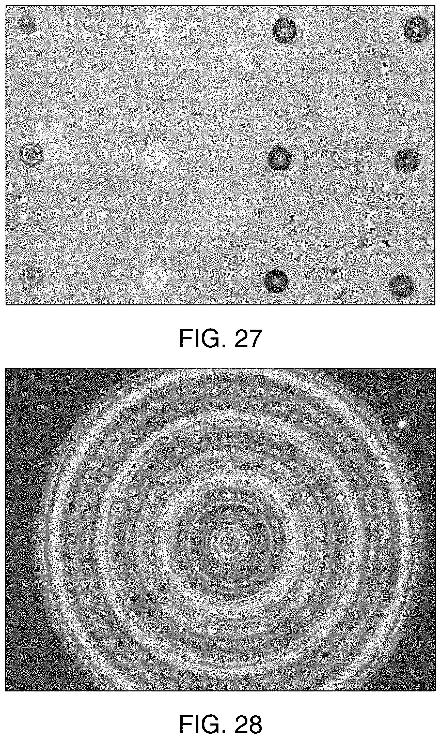
[0087] FIG. 27 provides an optical microscope image of an example chip with a number of amorphous-silicon near-IR metasurface lenses patterned on a quartz substrate. The diameters of the lenses are all 300 .mu.m. FIG. 28 provides an optical microscope image of an amorphous-silicon near-IR metasurface lenses patterned on a quartz substrate.
[0088] FIG. 29A shows optimization scheme for correcting both chromatic and monochromatic aberrations in a metalens triplet consisting of three individual metalenses. A ray-tracing method is used to optimize the metalens triplet. The goal of optimization is to minimize optical spot size at the focal plane at various incident angles and wavelengths. The phase profile of each metasurface is prescribed by an even order polynomial with 5 parameters, so in total 15 parameters are used for optimization. The following equation describes the phase profile:
.PHI. 1 = n = 1 5 An ( P R 1 ) 2 n ( 10 ) ##EQU00006##
[0089] FIG. 29B shows the phase profiles of the three metasurfaces for one particular realization of a metalens triplet. The first phase profile is given by the large U-shaped curve 2901, the second phase profile is given by the small upside down U shaped curve 2902, and the third phase profile is given by the large upside down U shaped curve 2903. Parameters for this particular realization are listed under the figure.
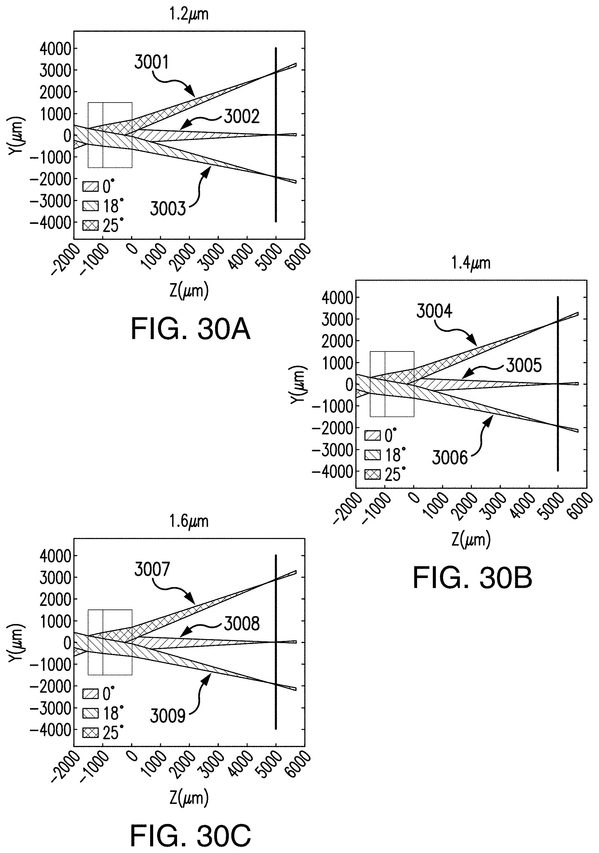
[0090] FIGS. 30A-30C are ray-tracing results showing good performance of a metalens triplet at three exemplary incident angles and three operation wavelengths. The left most graph with operation wavelength 1.2 .mu.m 3000, contains tree exemplary incident angles. The highest 3001 is 25 degrees; the middle 3002, is 0 degrees; and the lowest 3003 is 18 degrees. The middle graph with operation wavelength 1.4 .mu.m 3004, contains tree exemplary incident angles. The highest 3005 is 25 degrees; the middle 3006, is 0 degrees; and the lowest 3007 is 18 degrees. The left most graph with operation wavelength 1.6 .mu.m 3008, contains tree exemplary incident angles. The highest 3009 is 25 degrees; the middle 3010, is 0 degrees; and the lowest 3011 is 18 degrees. FIGS. 31A-31C are optical images of three elements of a metasurface triplet fabricated using electron-beam lithography and FIG. 32 is an optical image of the assembled triplet.
[0091] FIG. 33 shows measured far-field intensity distributions of the metalens triplet shown in FIG. 32. Measured light intensity distributions on the focal plane are shown in the top panel, showing that the focal spots are diffraction limited over a broad range of wavelengths. Measured light intensity distributions on the longitudinal plane are shown in the bottom panel, showing that the focal distances are about 5 mm over a wavelength of .lamda.=1.3-1.6 .mu.m. FIG. 34 shows measured intensity distributions on the focal plane at different wavelengths and a few incident angles for the metalens triplet shown in FIG. 32. The results show that up to 20 degrees of angle of incidence the focal spots have little distortion, which indicates good suppression of monochromatic aberrations. When incident angle increases to 25 degrees, the focal spots start to show distortion for the shortest wavelengths. The line scans of the focal spots illustrated in FIG. 35 shows the same story. Modulation transfer function (MTF) of the metalens triplet can be calculated by conducting Fourier transform of the measured focal spots, and the results are shown in FIGS. 36A-36E. FIGS. 36A-36D are MTFs calculated at four wavelengths. FIG. 36E shows MTFs integrated over the 1.3 to 1.6 .mu.m wavelength range at several incident angles. The MTF curves do not decrease significantly compared to the MTF of the diffraction-limited case as incident angle increases, which indicates that monochromatic aberrations are suppressed.
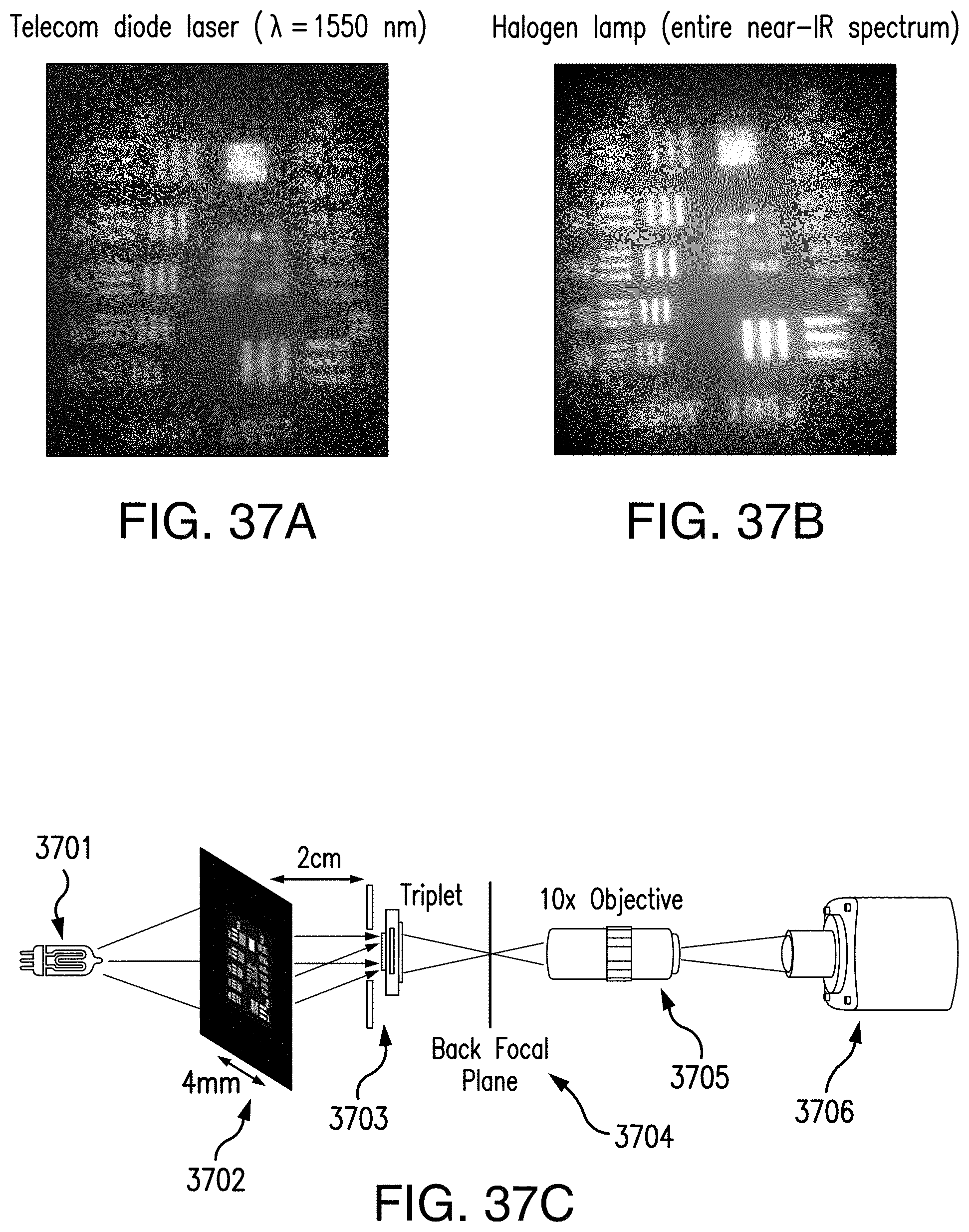
[0092] FIGS. 37A and 37B show results of imaging the USAF resolution target using the metalens triplet. FIG. 37A is an image taken with the target illuminated with a diode laser with very narrow linewidth around .lamda.=1550 nm. FIG. 37B is an image taken with the target illuminated with a broadband halogen lamp emitting broadband near-infrared radiation from .lamda.=700 nm to 1700 nm. Comparison of the two images shows that the image taken with the diode laser is sharper, but the degradation when the halogen lamp is used is not significant. This indicates that the metalens triplet can correct chromatic aberrations. FIG. 37C is a schematic of the experimental setup. The setup includes a fiber coupler 3701, a resulting image 3702, a triplet 3703, a back focal plane 3704, 10.times. Objective 3705, and a camera operating in the near-IR 3706.
[0093] FIGS. 38A and 38B show results of imaging of the Siemens star and concentric ring using the metalens triplet. FIG. 38A is an image taken with the target illuminated with the diode laser emitting at .lamda.=1550 nm. FIG. 38B is an image taken with the target illuminated with the broadband halogen lamp. The degradation of the image when the halogen lamp is used is not significant, indicating that the metalens triplet can correct chromatic aberrations. FIGS. 39A and 39B show results of imaging reflection type objects illuminated with the broadband halogen lamp using the metalens triplet. FIG. 39A is an image of Columbia Engineering logo printed on an A4 paper. The field of view is about .+-.15 degrees. FIG. 39B is an image of a USAF resolution target printed on an A4 paper. The field of view is also about .+-.15 degrees. The sharp features of the images indicate monochromatic aberrations have been suppressed. FIG. 39C is a schematic of the experimental setup. The setup includes a resulting image 3901, a fiber coupler 3902, a triplet 3903, a back focal plane 3904, 10x Objective 3905, and a camera operating in the near-IR 3906.
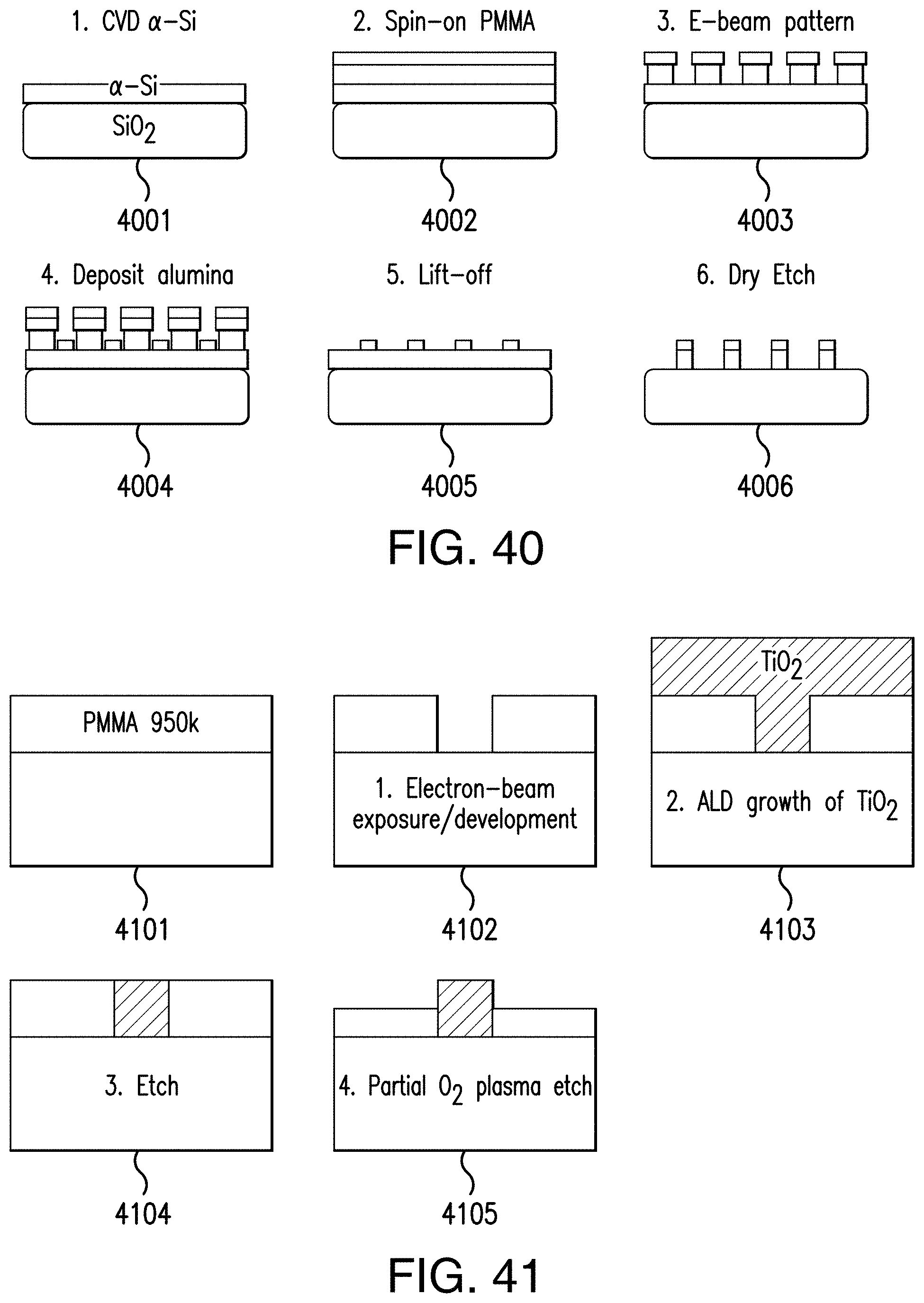
[0094] FIG. 40 illustrates an example fabrication flow for metasurface lenses 4000 based on amorphous silicon (a-Si) and operating in the near-infrared. Fabrication can be undertaken with processes compatible with complementary metal oxide semiconductor (CMOS) fabrication facilities. Materials used can include any CMOS compatible low-loss dielectric material operating within the bandwidth desired. This can make the choice of a-Si nanostructures resting on a silicon dioxide substrate. At 4001, the a-Si film can be grown atop the silicon dioxide substrate with chemical vapor deposition to heights of 100 to 10,000 nm. At 4002, electron-beam lithography (generalizable to optical lithography, deep UV lithography, or nanoimprint lithography) can be used to pattern the designed metasurface pattern into a resist layer (poly(methyl methacrylate), or PMMA) that can be deposited on top of the a-Si layer by a standard spin-deposition technique. At 4003, the patterns can be developed by submersion into a developing solution of Isopropyl alcohol and distilled water (3:1 to 6:4 ratio) at temperatures between 0 and 10 degrees Celsius, for a time between 1 and 3 minutes. At 4004, an etching mask material such as alumina or silica can be deposited by physical vapor deposition to a thickness of between 10 and 50 nm. At 4005, the pattern can be lifted off by dissolving the remaining resist layer in an organic solvent such as acetone or N-methyl-2-pyrrolidone at a temperature of between 25 and 90 degrees Celsius, for a time between 1 and 12 hours. At 4006, the material remaining atop the a-Si layer can be the etching mask determined by the electron-beam lithography. This pattern can be transferred into the a-Si layer by reactive ion etching, yielding the final device composed of silicon metasurfaces on silicon dioxide substrate after an optional process to remove the etching mask layer by a wet chemical process.
[0095] In some embodiments, fabrication of meta-units is disclosed. FIG. 41 provides an example fabrication flow of TiO.sub.2 meta-units (purple) for metasurface lenses. At 4101, a layer of electron-beam resist, e.g., PMMA 950 k, is spin coated. Next 4102, an electron beam exposure is applied to define metasurface lens patterns. At 4103, TiO.sub.2 is deposited using atomic layer deposition (ALD). At 4104, an etch is used to planarize the surface of the device. At 4105, a partial oxygen plasma etch is used to remove a layer of PMMA. Higher aspect ratio TiO.sub.2 meta-units can be allowed in this scheme due to being partially embedded in the PMMA resist layer for mechanical stability. The portion of the meta-units exposed to air can have large index contrast, yielding large coverage in the phase offset-dispersion space compared to meta-units purely embedded in the PMMA resist. Having partially embedded meta-units can allow overall taller structures, yielding larger coverage in the phase offset-dispersion space than removing the resist entirely.
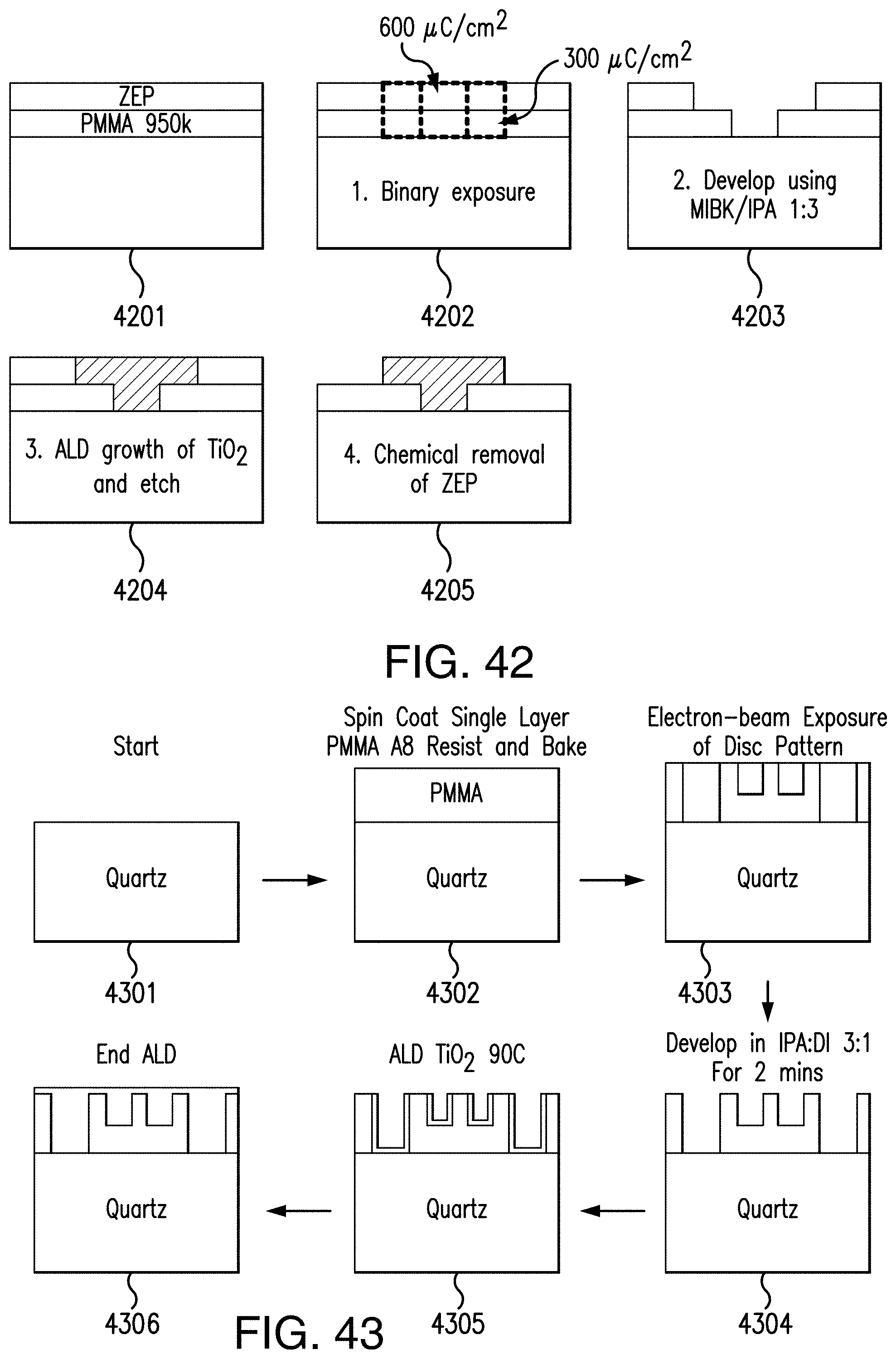
[0096] FIG. 42 provides an example fabrication flow of mushroom shaped TiO.sub.2 meta-units (purple) 4200 for metasurface lenses. A single electron-beam writing procedure can be used with two electron-beam resist layers offering orthogonal developing chemistries. At 4201, a dual layer of electron-beam resists consisting of PMMA 950 k and ZEP are spin coated. At 4202, binary electron beam exposure is applied over two regions of different sizes with different doses. At 4203, part of the electron beam resists are removed using MIBK and IPA. At 4204, TiO.sub.2 is deposited and the surface of the device is planarized. At 4205, ZEP is chemically removed. In some embodiments, a developer ratio of MIBK/IPA can be 1:3, where the top layer (ZEP) can be developed at a lower dosage than is required for the bottom layer (PMMA). This can allow a 3D shape to be fabricated in a single lithographic process, with variable cross sections in each layer (constrained such that the cross section of the top layer is larger than the cross section of the bottom layer).
[0097] FIG. 43 illustrates an example fabrication flow of TiO.sub.2 meta-units with variable height in a single lithographic procedure. At 4301, a quartz substrate is provided. At 4302, a single layer of electron beam resist PMMA is spin coated and the layer is baked. At 4303, a procedure employing electron beam exposure of the metasurface lens pattern is used. At 4304, a developing process in IPA/de-ionized water is used to remove exposed electron resist. At 4305, a layer of TiO.sub.2 is deposited using atomic layer deposition (ALD). Continued deposits of TiO.sub.2 and planarization of the surface of the device results at 4306. The "gray-scale" lithographic method can be applied to achieve a mold of resist (PMMA in this case) with variable depth. This can allow the vertical degree of freedom in a way similar to the mushroom shaped meta-units shown in FIG. 42.
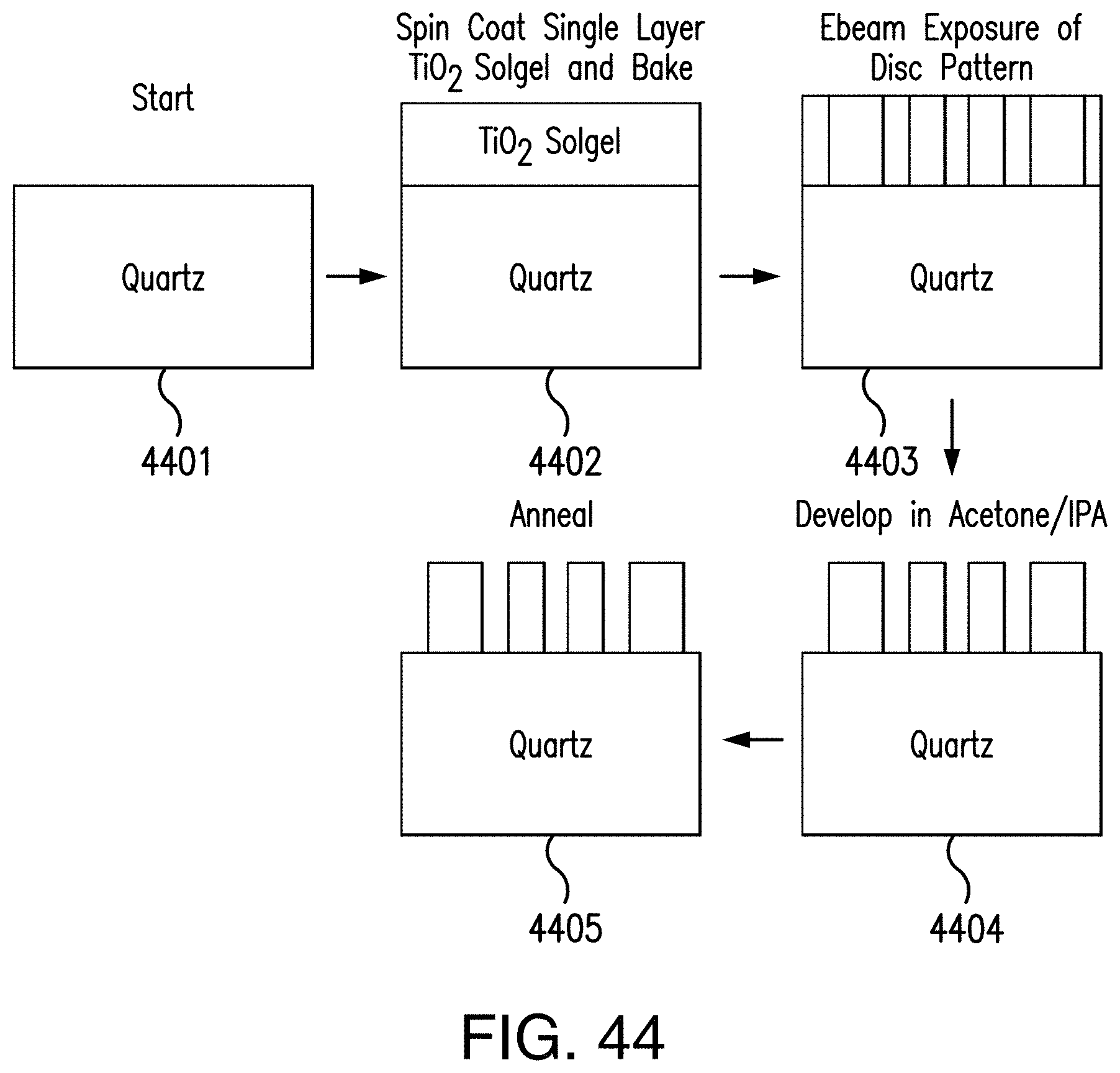
[0098] FIG. 44 provides an example fabrication flow of TiO.sub.2 meta-units using electron-beam sensitive TiO.sub.2 sol-gel. At 4401, a quartz substrate is provided. Next 4402, a single layer of TiO.sub.2 solgel is spin coated and baked. At 4403, a procedure employing electron beam exposure of the metasurface lenses is used. At 4404, a developing process in acetone/IPA is used. At 4405, the device is annealed to remove organic components. The sol-gel can behave like a negative resist with the electron-beam exposed regions becoming insoluble in acetone. Post development annealing can result in the formation of TiO.sub.2 nanostructures. The annealing process can result in shrinkage of the nanostructured due to evaporation of organic chemicals. For this fabrication process, deposition or etching can be avoided.
[0099] In some embodiments, an electron beam sensitive TiO.sub.2 sol-gel can be synthesized by mixing equimolar ratio of metal alkoxide precursor Titanium(IV) n-butoxide Ti(OBu.sup.n).sub.4 with .beta.-diketone 1-Benzoylacetone (BzAc) in ethanol solvent at room temperature and low humidity environment. BzAc can stabilize Ti(OBu.sub.n).sub.4 reducing its hydrolytic reactivity and forms chelate rings with it. When the chelate rings are broken due to exposure to electron beam, the sol-gel can be rendered insoluble to organic solvents like acetone. The resulting sol-gel nanostructures can be converted to pure TiO.sub.2 by annealing in the temperature range 300.degree.-500.degree. C. Other synthesis methods can involve adding glacial acetic to the previous solution to prevent precipitation during aging process.
[0100] FIG. 45 provides a SEM image of an example fabricated TiO.sub.2 meta-units based on direct electron-beam writing of TiO.sub.2 sol-gel. Cross shaped structures with 2-.mu.m arms and 2-.mu.m period were fabricated on a silicon substrate. This image was taken on Apr. 30, 2017 at 2:59:17 PM with the following values: HV=10.00 kV; spot=2.0; det=TLD; mode=SE; mag=20,000.times.; 6.35 .mu.m; WD=5.1 mm.
[0101] FIG. 46 provides a SEM image of fabricated TiO.sub.2 meta-units based on direct electron-beam writing of TiO.sub.2 sol-gel. Cross shaped structures with 2-.mu.m arms and 2-.mu.m period were fabricated on a silicon substrate viewed at 30.degree.. This image was taken on Apr. 30, 2017 at 3:20:13 PM with the following values: HV=10.00 kV; spot=2.0; det=TLD; mode=SE; mag=20,000.times.; 6.35 .mu.m; and WD=5.3 mm.
[0102] FIG. 47 provides a SEM image of fabricated TiO.sub.2 meta-units based on direct electron-beam writing of TiO.sub.2 sol-gel. Each meta-unit is a distinct element of our meta-unit library. This image was taken on May 11, 2017 at 19:02:36 PM with the following values: EHT=15.00 kV; Signal A=InLens; WD=3.1 mm; Mag=20.01 K X; Vac Status=Ready; Gun Vacuum=7.53e-010 mbar; and System Vacuum=3.14e-006 mbar.
[0103] In an exemplary embodiment of the disclosed subject matter, a schematic for depicting the optical setup is provided. Referring to FIG. 48, for the purpose of illustration and not limitation, the setup 4800 can include an NIR Camera 4801, an iris 4802, a tube lens 4803, a flip mirror 4804, a lens 4805, and a power meter 4806, all mounted onto a motorized stage 4807. A metalens 4808 and a fiber coupler 4809 can also be included. In some embodiments, the NIR camera 4801 takes in light that must pass first through the fiber coupler 4809, then through the metalens 4808, then through the tube lens 4803, and finally through the iris 4802. In some embodiments, a flip mirror 4804, allows passing the light from a lens 4805, to a power meter 4806, for efficiency measurements.
[0104] The description herein merely illustrates the principles of the disclosed subject matter. Various modifications and alterations to the described embodiments will be apparent to those skilled in the art in view of the teachings herein. Accordingly, the disclosure herein is intended to be illustrative, but not limiting, of the scope of the disclosed subject matter.
* * * * *
D00000
D00001
D00002
D00003
D00004
D00005
D00006
D00007
D00008
D00009
D00010
D00011
D00012
D00013
D00014
D00015
D00016
D00017
D00018
D00019
D00020
D00021

D00022
D00023
D00024
D00025
D00026

D00027
D00028

D00029

D00030
D00031
D00032
D00033
D00034
D00035


XML
uspto.report is an independent third-party trademark research tool that is not affiliated, endorsed, or sponsored by the United States Patent and Trademark Office (USPTO) or any other governmental organization. The information provided by uspto.report is based on publicly available data at the time of writing and is intended for informational purposes only.
While we strive to provide accurate and up-to-date information, we do not guarantee the accuracy, completeness, reliability, or suitability of the information displayed on this site. The use of this site is at your own risk. Any reliance you place on such information is therefore strictly at your own risk.
All official trademark data, including owner information, should be verified by visiting the official USPTO website at www.uspto.gov. This site is not intended to replace professional legal advice and should not be used as a substitute for consulting with a legal professional who is knowledgeable about trademark law.