Composite Thermistor Chip And Preparation Method Thereof
DUAN; Zhaoxiang ; et al.
U.S. patent application number 16/618949 was filed with the patent office on 2020-03-19 for composite thermistor chip and preparation method thereof. The applicant listed for this patent is EXSENSE ELECTRONICS TECHNOLOGY CO., LTD.. Invention is credited to Qixing BAI, Zhaoxiang DUAN, Limin TANG, Jun YANG, Jiankai YE.
| Application Number | 20200090840 16/618949 |
| Document ID | / |
| Family ID | 62210296 |
| Filed Date | 2020-03-19 |


| United States Patent Application | 20200090840 |
| Kind Code | A1 |
| DUAN; Zhaoxiang ; et al. | March 19, 2020 |
COMPOSITE THERMISTOR CHIP AND PREPARATION METHOD THEREOF
Abstract
A composite thermistor chip includes a thermosensitive ceramic chip, a metal electrode and a glass glaze resistor, wherein the thermosensitive ceramic chip has a front side and a back side, the metal electrode includes a first terminal electrode, a second terminal electrode and a third electrode layer; the first terminal electrode and the second terminal electrode are respectively arranged at two ends of the front side of the thermosensitive ceramic chip, and the glass glaze resistor is arranged on the front side of the thermosensitive ceramic chip, two ends of the glass glaze resistor are respectively connected to the first terminal electrode and the second terminal electrode; and the back side of the thermosensitive ceramic chip is covered with the third electrode layer.
| Inventors: | DUAN; Zhaoxiang; (Zhaoqing City, Guangdong, CN) ; YE; Jiankai; (Zhaoqing City, Guangdong, CN) ; YANG; Jun; (Zhaoqing City, Guangdong, CN) ; BAI; Qixing; (Zhaoqing City, Guangdong, CN) ; TANG; Limin; (Zhaoqing City, Guangdong, CN) | ||||||||||
| Applicant: |
|
||||||||||
|---|---|---|---|---|---|---|---|---|---|---|---|
| Family ID: | 62210296 | ||||||||||
| Appl. No.: | 16/618949 | ||||||||||
| Filed: | October 31, 2018 | ||||||||||
| PCT Filed: | October 31, 2018 | ||||||||||
| PCT NO: | PCT/CN2018/112857 | ||||||||||
| 371 Date: | December 3, 2019 |
| Current U.S. Class: | 1/1 |
| Current CPC Class: | H01C 7/042 20130101; G01K 7/22 20130101; H01C 1/1413 20130101; H01C 17/30 20130101; H01C 7/041 20130101; H01C 17/006 20130101; H01C 17/065 20130101; H01C 17/281 20130101; H01C 1/142 20130101 |
| International Class: | H01C 1/14 20060101 H01C001/14; H01C 1/142 20060101 H01C001/142; H01C 17/00 20060101 H01C017/00; H01C 7/04 20060101 H01C007/04; G01K 7/22 20060101 G01K007/22 |
Foreign Application Data
| Date | Code | Application Number |
|---|---|---|
| Dec 20, 2017 | CN | 201711380975.1 |
Claims
1-10. (canceled)
11. A composite thermistor chip, comprising a thermosensitive ceramic chip, a metal electrode and a glass glaze resistor; the thermosensitive ceramic chip has a front side and a back side; the metal electrode comprises a first terminal electrode, a second terminal electrode and a third electrode layer; the first terminal electrode and the second terminal electrode are respectively arranged at two ends of the front side of the thermosensitive ceramic chip; the glass glaze electrode is arranged on the front side of the thermosensitive ceramic chip, two ends of the glass glaze resistor are respectively connected to the first terminal electrode and the second terminal electrode; and the back side of the thermosensitive ceramic chip is covered with the third electrode layer.
12. The composite thermistor chip of claim 11, wherein the metal electrode is made from a precious metal.
13. The composite thermistor chip of claim 11, wherein the thermosensitive ceramic chip is made from a negative temperature coefficient thermosensitive ceramic material.
14. The composite thermistor chip of claim 11, wherein the glass glaze resistor is prepared by printing and sintering glass glaze resistor paste on the thermosensitive ceramic chip.
15. A preparation method of the composite thermistor chip of claim 11, comprising following steps: (1) mixing raw materials according to a conventional negative temperature coefficient thermosensitive ceramic material formula, and then sequentially ball-milling, drying, screening, pre-sintering, grinding, drying and screening the raw materials to prepare negative temperature coefficient thermosensitive ceramic powder for later use; (2) placing the prepared negative temperature coefficient thermosensitive ceramic powder into a mold, placing the mold in an isostatic press to press the negative temperature coefficient therniosensitive ceramic powder, taking a formed ceramic ingot out of the mold after pressure relief, then sintering the ceramic ingot, and afterwards, slicing the ceramic ingot to obtain a thermosensitive ceramic substrate; (3) printing a metal electrode layer on a surface of the thermosensitive ceramic substrate; (4) printing glass glaze resistor pastes on the surface of the thermosensitive ceramic substrate, and conducting sintering after the glass glaze resistor pastes are dried to obtain glass glaze resistors printed on the thermosensitive ceramic substrate; and (5) conducting laser resistance trimming on the glass glaze resistors, and then dividing the thermosensitive ceramic substrate to obtain single composite thermistor chips.
16. The preparation method of claim 15, wherein in step (2), the negative temperature coefficient thermosensitive ceramic powder is pressed in the isostatic press at a pressure of 200-400 MPa for 10-50 s.
17. The preparation method of claim 15, wherein in step (4), sintering is conducted at a temperature of 800-900.degree. C. for 10-30 min.
Description
CROSS REFERENCE TO RELATED APPLICATIONS
[0001] This application is a national application of PCT/CN2018/112857, filed on Oct. 31, 2018. The contents of PCT/CN2018/112857 are all hereby incorporated by reference.
FIELD OF TECHNOLOGY
[0002] The following relates to the technical field of electronic components, in particular to a composite thermistor chip and a preparation method thereof.
BACKGROUND
[0003] With the innovation of electronic products, more and more electronic products have possessed a temperature sensing or detection function, wherein the core component used to fulfill temperature detection is a thermistor chip. Due to the fact that the resistance of the thermistor chips varies with temperature variations, the temperature of a position where the thermistor chips are located can be determined in terms of the resistance of the thermistor chips, so as to fulfill temperature sensing or detection.
[0004] FIG. 1 is a structural view of a conventional thermistor chip. As shown in FIG. 1, the conventional thermistor chip includes a thermosensitive ceramic chip 1' and metal electrodes 2' printed on two surfaces of the thermosensitive ceramic chip 1'. As shown in FIG. 2, a method for preparing the conventional thermistor chip includes the steps: preparation of thermosensitive ceramic powder, sintering of a ceramic ingot, slicing, printing of precious metal electrodes, sintering, size calculation and cutting.
SUMMARY
[0005] An aspect relates to a composite thermistor chip which has an adjustable characteristic temperature curve and is simple in structure, easy to prepare, and low in cost.
[0006] The technical solution adopted in embodiments as follows:
[0007] A composite thermistor chip includes a thermosensitive ceramic chip, a metal electrode and a glass glaze resistor, wherein the thermosensitive ceramic chip has a front side and a back side, the metal electrode includes a first terminal electrode and a second terminal electrode, the first terminal electrode and the second terminal electrode are respectively arranged at two ends of either the front side or the back side of the thermosensitive ceramic chip, and the glass glaze resistor is arranged on the front side or the back side of the thermosensitive ceramic chip.
[0008] In some embodiments, the metal electrode further includes a third electrode layer; the first terminal electrode, the second terminal electrode, and the glass glaze resistor are all arranged on the front side of the thermosensitive ceramic chip; two ends of the glass glaze resistor are respectively connected to the first terminal electrode and the second terminal electrode; and the back side of the thermosensitive ceramic chip is covered with the third electrode layer. In this case, an equivalent circuit of the composite thermistor chip can be regarded as a circuit structure formed by a fixed resistor and two cascading thermistors connected with the fixed resistor in parallel.
[0009] In some embodiments, the glass glaze resistor is arranged on the front side of the thermosensitive ceramic chip, and the first terminal electrode and the second terminal electrode are respectively arranged at two ends of the back side of the thermosensitive ceramic chip. In this case, an equivalent circuit of the composite thermistor chip can be regarded as a circuit structure formed by a fixed resistor and two thermistors connected with the fixed resistor in series.
[0010] Furthermore, the metal electrode is made from a precious metal.
[0011] Furthermore, the thermosensitive ceramic chip is made from an NTC thermosensitive ceramic material ("NTC" is the abbreviation of "negative temperature coefficient").
[0012] Furthermore, the glass glaze resistor is prepared by printing and sintering glass glaze resistor paste on the thermosensitive ceramic chip.
[0013] Embodiments of the disclosure also disclose a preparation method of any one of the composite thermistor chips mentioned above. The preparation method includes the following steps: pressing NTC thermosensitive ceramic powder and then sintering the NTC thermosensitive ceramic powder to form a ceramic ingot, cutting the ceramic ingot into a thermosensitive ceramic substrate, printing a metal electrode layer and glass glaze resistors on the thermosensitive ceramic substrate, then sintering the thermosensitive ceramic substrate, and afterwards, dividing the sintered thermosensitive ceramic substrate to obtain single composite thermistor chips.
[0014] Furthermore, the preparation method specifically includes the following steps:
[0015] (1) Mixing raw materials according to a conventional NTC thermosensitive ceramic material formula, and then sequentially ball-milling, drying, screening, pre-sintering, grinding, drying and screening the raw materials to prepare NTC thermosensitive ceramic powder for later use;
[0016] (2) Placing the prepared NTC thermosensitive ceramic powder into a mold, placing the mold in an isostatic press to press the NTC thermosensitive ceramic powder, taking a formed ceramic ingot out of the mold after pressure relief, then sintering the ceramic ingot, and afterwards, slicing the ceramic ingot to obtain a thermosensitive ceramic substrate;
[0017] (3) Printing a metal electrode layer on a surface of the thermosensitive ceramic substrate;
[0018] (4) Printing glass glaze resistor pastes on the surface of the thermosensitive ceramic substrate, and conducting sintering after the glass glaze resistor pastes are dried to obtain glass glaze resistors printed on the thermosensitive ceramic substrate; and
[0019] (5) Conducting laser resistance trimming on the glass glaze resistors, and then dividing the thermosensitive ceramic substrate to obtain single composite thermistor chips.
[0020] Furthermore, in step (2), the NTC thermosensitive ceramic powder is pressed in the isostatic press at a pressure of 200-400 MPa for 10-50 s.
[0021] Furthermore, in step (4), sintering is conducted at a temperature of 800-900.degree. C. for 10-30 min, and the metal electrode layer and the glass glaze resistor pastes are sintered at the same time.
[0022] For the sake of a better understanding and implementation, embodiments of the disclosure are detailed below in combination with the accompanying drawings.
BRIEF DESCRIPTION OF THE DRAWINGS
[0023] FIG. 1 is a structural view of a conventional thermistor chip;
[0024] FIG. 2 is a flow diagram of a preparation process of the conventional thermistor chip;
[0025] FIG. 3 is a structural view of a composite thermistor chip in Embodiment 1;
[0026] FIG. 4 is an equivalent circuit diagram of the composite thermistor chip in Embodiment 1;
[0027] FIG. 5 is a structural view of a composite thermistor chip in Embodiment 2;
[0028] FIG. 6 is an equivalent circuit diagram of the composite thermistor chip in Embodiment 2;
[0029] FIG. 7 is a flow diagram of a preparation method in Embodiment 3;
[0030] FIG. 8 is a comparison diagram of the resistance-temperature curves of the composite thermistor chip in Embodiment 1, the composite thermistor chip in Embodiment 2, and the conventional thermistor chip.
DETAILED DESCRIPTION
Embodiment 1
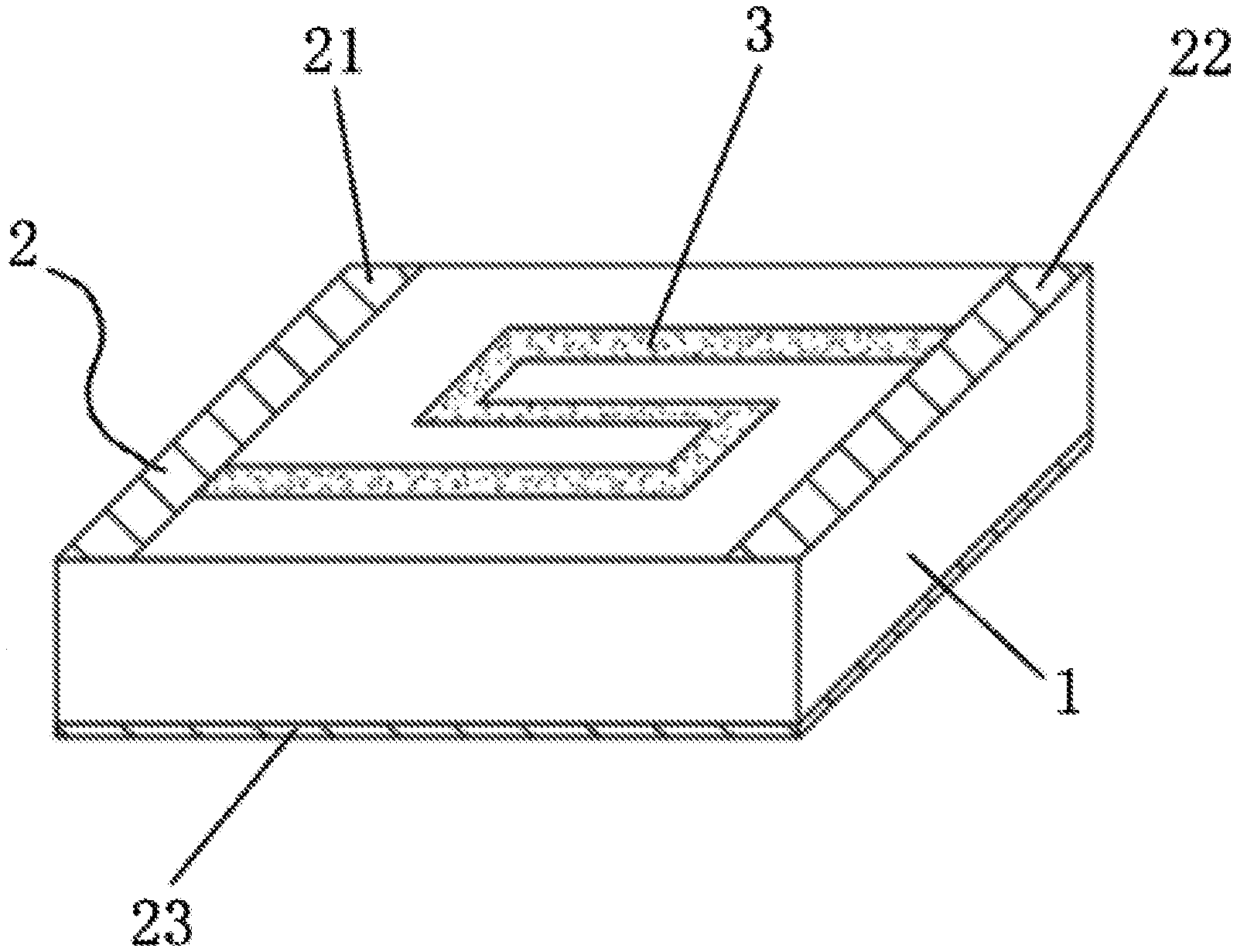
[0031] Please refer to FIG. 3, which is a structural view of a composite thermistor chip in this embodiment.
[0032] In this embodiment, the composite thermistor chip includes a thermosensitive ceramic chip 1, a metal electrode 2, and a glass glaze resistor 3.
[0033] The thermosensitive ceramic chip 1 is a rectangular ceramic chip, has two surfaces respectively serving as a front side and a back side, and has a thickness of 200-2000 .mu.m.
[0034] The metal electrode 2 includes a first terminal electrode 21, a second terminal electrode 22, and a third electrode layer 23. The first terminal electrode 21 and the second terminal electrode 22 are respectively arranged at two ends of the front side of the thermosensitive ceramic chip 1. The back side of the thermosensitive ceramic chip 1 is covered with the third electrode layer 23.
[0035] The glass glaze resistor 3 is arranged on the front side of the thermosensitive ceramic chip 1 and has two ends respectively connected to the first terminal electrode 21 and the second terminal electrode 22. The resistance of the glass glaze resistor 3 is 10 k.OMEGA..
[0036] Specifically, the thermosensitive ceramic chip 1 is made from an NTC thermosensitive ceramic material having a material constant of B(25/85)=3435K, and the NTC thermosensitive ceramic material is prepared by sintering metal oxides such as the oxide of manganese, cobalt, nickel, copper and iron, etc. The metal electrode 2 is made from a precious metal and is preferably made from sliver. The glass glaze resistor 3 is prepared by printing and sintering glass glaze resistor paste on the thermosensitive ceramic chip 1 and is easy to prepare, and the printing form can be adjusted according to actual requirements. The glass glaze resistance paste is a marketable product, which is composed of metal oxide, glass powder and organic binder, and the metal oxide is the oxide of precious metals such as silver, palladium, ruthenium, rhodium, etc.
[0037] The first terminal electrode 21 and the second terminal electrode 22 respectively serve as a positive electrode and a negative electrode. FIG. 4 is an equivalent circuit diagram of the composite thermistor chip in this embodiment, wherein the glass glaze resistor 3 is equivalent to a fixed resistor R, the thermosensitive ceramic chip 1 is equivalent to two cascading thermistors RT connected with the fixed resistor R in parallel.
Embodiment 2
[0038] Please refer to FIG. 5, which is a structural view of a composite thermistor chip in this embodiment.
[0039] In this embodiment, the composite thermistor chip includes a thermosensitive ceramic chip 1, a metal electrode 2, and a glass glaze resistor 3.
[0040] The thermosensitive ceramic chip 1 is a rectangular ceramic chip, has two surfaces respectively serving as a front side and a back side, and has a thickness of 200-2000 .mu.m.
[0041] The metal electrode 2 includes a first terminal electrode 21 and a second terminal electrode 22. The first terminal electrode 21 and the second terminal electrode 22 are respectively arranged at two ends of the back side of the thermosensitive ceramic chip 1.
[0042] The glass glaze resistor 3 is arranged on the front side of the thermosensitive ceramic chip 1. The resistance of the glass glaze resistor 3 is 10 k.OMEGA..
[0043] Specifically, the thermosensitive ceramic chip 1 is made from an NTC thermosensitive ceramic material having a material constant of B(25/85)=3435K, and the NTC thermosensitive ceramic material is prepared by sintering metal oxides such as the oxide of manganese, cobalt, nickel, copper and iron, etc. The metal electrode 2 is made from a precious metal and is preferably made from sliver. The glass glaze resistor 3 is prepared by printing and sintering glass glaze resistor paste on the thermosensitive ceramic chip 1 and is easy to prepare, and the printing form can be adjusted according to actual requirements. The glass glaze resistance paste is a marketable product, which is composed of metal oxide, glass powder and organic binder, and the metal oxide is the oxide of precious metals such as silver, palladium, ruthenium, rhodium, etc.
[0044] The first terminal electrode 21 and the second terminal electrode 22 respectively serve as a positive electrode and a negative electrode. FIG. 6 is an equivalent circuit diagram of the composite thermistor chip in this embodiment, wherein the glass glaze resistor 3 is equivalent to a fixed resistor R, the thermosensitive ceramic chip 1 is equivalent to two thermistors RT connected with the fixed resistor R in series.
Embodiment 3
[0045] Please refer to FIG. 7 which is a flow diagram of a preparation method in this embodiment.
[0046] In this embodiment, a preparation method of the composite thermistor chip in Embodiment 1 or the composite thermistor chip in Embodiment 2 specifically includes the following steps:
[0047] (1) Mixing raw materials according to a conventional NTC thermosensitive ceramic material formula, and then sequentially ball-milling, drying, screening, pre-sintering, grinding, drying and screening the raw materials to prepare NTC thermosensitive ceramic powder 4 for later use;
[0048] (2) Loosely placing the prepared NTC thermosensitive ceramic powder 4 into a rubber mold, then compacting the NTC thermosensitive ceramic powder 4, and afterwards, placing the rubber mold in an isostatic press to press the NTC thermosensitive ceramic powder 4 under a pressure of 200-400 MPa for 10-50 s, taking a formed cuboid ceramic ingot 5 out of the mold after pressure relief, then sintering the ceramic ingot 5 at a temperature to obtain a compact ceramic ingot 5, and afterwards, using an inner diameter slicer to slice the ceramic ingot 5 in terms of a set thickness to obtain a thermosensitive ceramic substrate 6;
[0049] (3) Printing silver pastes on a surface of the thermosensitive ceramic substrate 6, and drying the silver pastes to obtain a silver metal electrode layer 20 printed on the thermosensitive ceramic substrate 6;
[0050] Specifically, when the composite thermistor chip in Embodiment 1 is prepared, the metal electrode layer 20 includes a plurality of parallel terminal electrodes printed on a front side of the thermosensitive ceramic substrate 6 and an electrode layer printed on a whole back side of the thermosensitive ceramic substrate 6; or
[0051] when the composite thermistor chip in Embodiment 2 is prepared, the metal electrode layer 20 includes a plurality of parallel terminal electrodes printed on the back side of the thermosensitive ceramic substrate 6;
[0052] (4) Printing glass glaze resistor pastes on the surface of the thermosensitive ceramic substrate 6 in a form that can be adjusted according to a desired resistance and the area of the thermosensitive ceramic substrate 6; and conducting sintering at a temperature of 840.degree. C. for 10-30 min after the glass glaze resistor pastes are dried to obtain a plurality of glass glaze resistors 3 printed on the thermosensitive ceramic substrate 6;
[0053] Specifically, when the composite thermistor chip in Embodiment 1 is prepared, the glass glaze resistors 3 are printed on the front side of the thermosensitive ceramic substrate 6 and arrayed in a matrix manner, and two ends of each glass glaze resistor 3 are respectively connected to two adjacent terminal electrodes; or
[0054] when the composite thermistor chip in Embodiment 2 is prepared, the glass glaze resistors 3 are printed on the front side of the thermosensitive ceramic substrate 6 and arrayed in a matrix manner;
[0055] (5) Conducting laser resistance trimming on the glass glaze resistors 3 to improve resistance precision, and then dividing the thermosensitive ceramic substrate 6 to obtain single composite thermistor chips, wherein:
[0056] the thermosensitive ceramic substrate 6 is divided into thermosensitive ceramic chips 1, the metal electrode layer 20 is divided into metal electrodes 2, and each composite thermistor chip includes one glass glaze resistor 3.
[0057] The preparation method includes few steps and has only one extra step of printing the glass glaze resistors compared with the method for preparing the conventional thermistor chip, thereby being easy to implement and low in preparation cost; and the printing positions of the metal resistor and the glass glaze resistor can be adjusted as needed, so that the composite thermistor chip having a desired resistant-temperature curve is obtained.
[0058] The resistant-temperature curves (RT curves) of the composite thermistor chip in Embodiment 1, the composite thermistor chip in Embodiment 2, and the conventional thermistor chip are obtained by testing. The conventional thermistor chip is made from an NTC thermosensitive ceramic material having a material constant of B(25/85)=3435K, and the composite thermistor chip in Embodiment 1, the composite thermistor chip in Embodiment 2 and the conventional thermistor chip are identical in specification and size.
[0059] As shown in FIG. 8, the RT curves of the composite thermistor chip in Embodiment 1 and the composite thermistor chip in Embodiment 2 are different and deviate from the RT curve of the conventional thermistor chip, which means that a new temperature characteristic curve can be formed by disposing the glass glaze resistors 3 at different positions, and accordingly, thermistors having different applications and functions are obtained.
[0060] The glass glaze resistor is added to form the novel composite thermistor chip, wherein the glass glaze resistor is made from a material different from that of the thermosensitive ceramic chip, has a small temperature coefficient and can be regarded as a fixed resistor, so that the composite thermistor chip has a temperature characteristic curve different from that of the conventional thermistor chip; the temperature characteristic curve of the composite thermistor chip not only depends on a formula of a thermosensitive ceramic material adopted by the composite thermistor chip, but also depends on the resistance and position of the glass glaze resistor, as well as the position of the metal electrode, so that the temperature characteristic curve of the composite thermistor chip is adjustable, thus, satisfying different usage requirements and special production requirements which cannot be met by conventional thermistor chips.
[0061] On the whole, the glass glaze resistor serving as a fixed resistor is added to the circuit in series/parallel, so that the temperature characteristic curve of the thermosensitive ceramic chip can be greatly changed to obtain different temperature characteristic curves, and new applications and functions are achieved.
[0062] The embodiments which are specifically detailed above are only several illustrative ones of the invention and should not be regarded as restrictive to the patent scope of the invention. It should be noted that various transformations and improvements achieved by those ordinarily skilled in this field without deviating from the concept of the invention also fall within the protection scope of the invention.
* * * * *
D00000
D00001
D00002
D00003
D00004
D00005
D00006
XML
uspto.report is an independent third-party trademark research tool that is not affiliated, endorsed, or sponsored by the United States Patent and Trademark Office (USPTO) or any other governmental organization. The information provided by uspto.report is based on publicly available data at the time of writing and is intended for informational purposes only.
While we strive to provide accurate and up-to-date information, we do not guarantee the accuracy, completeness, reliability, or suitability of the information displayed on this site. The use of this site is at your own risk. Any reliance you place on such information is therefore strictly at your own risk.
All official trademark data, including owner information, should be verified by visiting the official USPTO website at www.uspto.gov. This site is not intended to replace professional legal advice and should not be used as a substitute for consulting with a legal professional who is knowledgeable about trademark law.