Semiconductor Device And Method For Manufacturing The Same
YAMAZAKI; Shunpei ; et al.
U.S. patent application number 16/674161 was filed with the patent office on 2020-03-05 for semiconductor device and method for manufacturing the same. The applicant listed for this patent is Semiconductor Energy Laboratory Co., Ltd.. Invention is credited to Masayuki SAKAKURA, Shunpei YAMAZAKI.
| Application Number | 20200075635 16/674161 |
| Document ID | / |
| Family ID | 43426798 |
| Filed Date | 2020-03-05 |


View All Diagrams
| United States Patent Application | 20200075635 |
| Kind Code | A1 |
| YAMAZAKI; Shunpei ; et al. | March 5, 2020 |
SEMICONDUCTOR DEVICE AND METHOD FOR MANUFACTURING THE SAME
Abstract
It is an object to manufacture and provide a highly reliable display device including a thin film transistor with a high aperture ratio which has stable electric characteristics. In a manufacturing method of a semiconductor device having a thin film transistor in which a semiconductor layer including a channel formation region is formed using an oxide semiconductor film, a heat treatment for reducing moisture and the like which are impurities and for improving the purity of the oxide semiconductor film (a heat treatment for dehydration or dehydrogenation) is performed. Further, an aperture ratio is improved by forming a gate electrode layer, a source electrode layer, and a drain electrode layer using conductive films having light transmitting properties.
| Inventors: | YAMAZAKI; Shunpei; (Setagaya, JP) ; SAKAKURA; Masayuki; (Tochigi, JP) | ||||||||||
| Applicant: |
|
||||||||||
|---|---|---|---|---|---|---|---|---|---|---|---|
| Family ID: | 43426798 | ||||||||||
| Appl. No.: | 16/674161 | ||||||||||
| Filed: | November 5, 2019 |
Related U.S. Patent Documents
| Application Number | Filing Date | Patent Number | ||
|---|---|---|---|---|
| 16191952 | Nov 15, 2018 | 10522568 | ||
| 16674161 | ||||
| 15695162 | Sep 5, 2017 | 10157936 | ||
| 16191952 | ||||
| 15342373 | Nov 3, 2016 | 9754974 | ||
| 15695162 | ||||
| 14730259 | Jun 4, 2015 | 9490277 | ||
| 15342373 | ||||
| 14486187 | Sep 15, 2014 | 9054138 | ||
| 14730259 | ||||
| 13856590 | Apr 4, 2013 | 8835920 | ||
| 14486187 | ||||
| 13658201 | Oct 23, 2012 | 8441011 | ||
| 13856590 | ||||
| 12832334 | Jul 8, 2010 | 8324027 | ||
| 13658201 | ||||
| Current U.S. Class: | 1/1 |
| Current CPC Class: | H01L 2924/0002 20130101; H01L 27/1225 20130101; H01L 33/42 20130101; H01L 21/02565 20130101; H01L 29/7869 20130101; H01L 27/124 20130101; H01L 27/1255 20130101; H01L 27/1248 20130101; H01L 21/02554 20130101; H01L 2924/0002 20130101; H01L 2924/00 20130101; H01L 29/66969 20130101 |
| International Class: | H01L 27/12 20060101 H01L027/12; H01L 21/02 20060101 H01L021/02; H01L 29/786 20060101 H01L029/786; H01L 33/42 20060101 H01L033/42; H01L 29/66 20060101 H01L029/66 |
Foreign Application Data
| Date | Code | Application Number |
|---|---|---|
| Jul 10, 2009 | JP | 2009-164265 |
Claims
1. (canceled)
2. A method for manufacturing a semiconductor device comprising the steps of: forming a gate electrode; forming a gate insulating layer over the gate electrode; forming an oxide semiconductor layer over the gate insulating layer; performing a first heat treatment at a temperature higher than or equal to 400.degree. C. on the oxide semiconductor layer, whereby a carrier concentration of the oxide semiconductor layer is increased; forming a source electrode and a drain electrode over the oxide semiconductor layer after the first heat treatment; forming an oxide insulating layer over and in contact with a part of the oxide semiconductor layer, whereby the carrier concentration of the oxide semiconductor layer is decreased; and performing a second heat treatment after forming the oxide insulating layer, wherein the part of the oxide semiconductor layer has a carrier concentration of less than 1.times.10.sup.18/cm.sup.3 after the second heat treatment, and wherein the source electrode and the drain electrode each comprises a conductive film having a light-transmitting property.
3. The method for manufacturing a semiconductor device according to claim 2, wherein the first heat treatment is performed under a nitrogen atmosphere, a rare gas atmosphere, or an oxygen atmosphere.
4. The method for manufacturing a semiconductor device according to claim 3, further comprising a step of cooling the oxide semiconductor layer after the first heat treatment under the oxygen atmosphere.
5. The method for manufacturing a semiconductor device according to claim 2, wherein the first heat treatment is performed under reduced pressure.
6. The method for manufacturing a semiconductor device according to claim 2, wherein the carrier concentration of the oxide semiconductor layer increased by the first heat treatment is higher than or equal to 1.times.10.sup.18/cm.sup.3 by the first heat treatment.
7. The method for manufacturing a semiconductor device according to claim 2, wherein the gate electrode comprises a transparent conductive film.
8. The method for manufacturing a semiconductor device according to claim 2, wherein the oxide semiconductor layer comprises indium, gallium and zinc.
9. The method for manufacturing a semiconductor device according to claim 2, wherein a temperature of the second heat treatment is higher than or equal to 150.degree. C. and lower than 350.degree. C.
10. The method for manufacturing a semiconductor device according to claim 2, further comprising a step of forming a pixel electrode over the oxide insulating layer, wherein the pixel electrode is electrically connected to one of the source electrode and the drain electrode.
11. The method for manufacturing a semiconductor device according to claim 10, wherein the part of the oxide semiconductor layer comprises a channel formation region, and wherein the pixel electrode overlaps with the channel formation region.
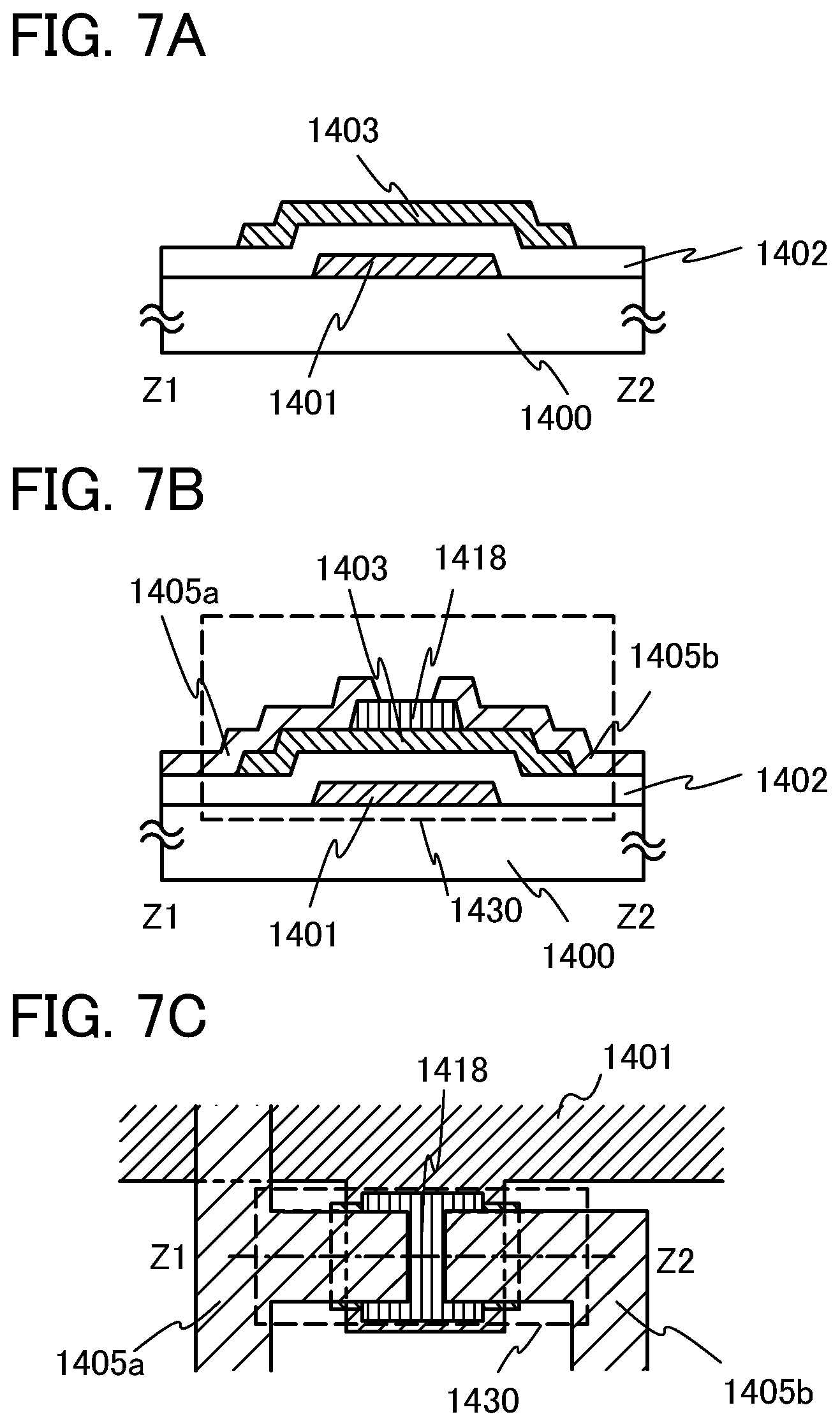
12. A method for manufacturing a semiconductor device comprising the steps of: forming a gate electrode; forming a gate insulating layer over the gate electrode; forming an oxide semiconductor layer over the gate insulating layer; performing dehydration or dehydrogenation on the oxide semiconductor layer by a first heat treatment at a temperature of higher than or equal to 400.degree. C., whereby a carrier concentration of the oxide semiconductor layer is increased; forming a source electrode and a drain electrode over the oxide semiconductor layer after the first heat treatment; forming an oxide insulating layer over and in contact with a part of the oxide semiconductor layer, whereby the carrier concentration of the oxide semiconductor layer is decreased; and performing a second heat treatment after forming the oxide insulating layer, wherein the part of the oxide semiconductor layer has a carrier concentration of less than 1.times.10.sup.18/cm.sup.3 after the second heat treatment, and wherein the source electrode and the drain electrode each comprises a conductive film having a light-transmitting property.
13. The method for manufacturing a semiconductor device according to claim 12, wherein the first heat treatment is performed under a nitrogen atmosphere, a rare gas atmosphere, or an oxygen atmosphere.
14. The method for manufacturing a semiconductor device according to claim 13, further comprising a step of cooling the oxide semiconductor layer after the first heat treatment under the oxygen atmosphere.
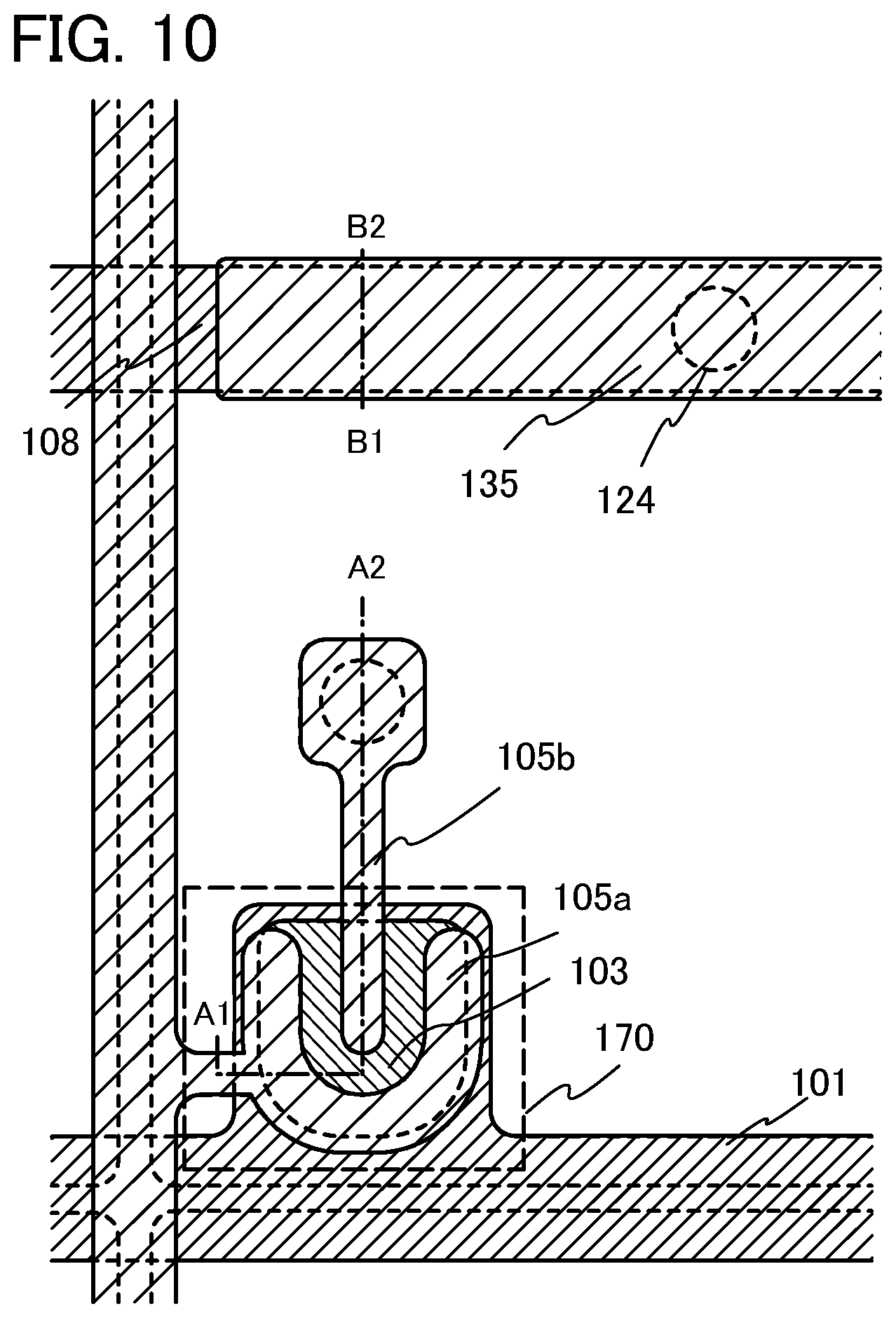
15. The method for manufacturing a semiconductor device according to claim 12, wherein the first heat treatment is performed under reduced pressure.
16. The method for manufacturing a semiconductor device according to claim 12, wherein the carrier concentration of the oxide semiconductor layer increased by the first heat treatment is higher than or equal to 1.times.10.sup.18/cm.sup.3 by the first heat treatment.
17. The method for manufacturing a semiconductor device according to claim 12, wherein the gate electrode comprises a transparent conductive film.
18. The method for manufacturing a semiconductor device according to claim 12, wherein the oxide semiconductor layer comprises indium, gallium and zinc.
19. The method for manufacturing a semiconductor device according to claim 12, wherein a temperature of the second heat treatment is higher than or equal to 150.degree. C. and lower than 350.degree. C.
20. The method for manufacturing a semiconductor device according to claim 12, further comprising a step of forming a pixel electrode over the oxide insulating layer, wherein the pixel electrode is electrically connected to one of the source electrode and the drain electrode.
21. The method for manufacturing a semiconductor device according to claim 20, wherein the part of the oxide semiconductor layer comprises a channel formation region, and wherein the pixel electrode overlaps with the channel formation region.
Description
TECHNICAL FIELD
[0001] The present invention relates to a semiconductor device having a circuit formed using a thin film transistor (hereinafter referred to as TFT) and a manufacturing method thereof. For example, the present invention relates to electro-optical devices typified by liquid crystal display panels, or electronic devices which have light-emitting display devices containing an organic light-emitting element as a component.
[0002] Note that in this specification, a semiconductor device refers to all devices that can function by utilizing semiconductor characteristics. An electro-optical device, a semiconductor circuit, and an electronic appliance are all semiconductor devices.
BACKGROUND ART
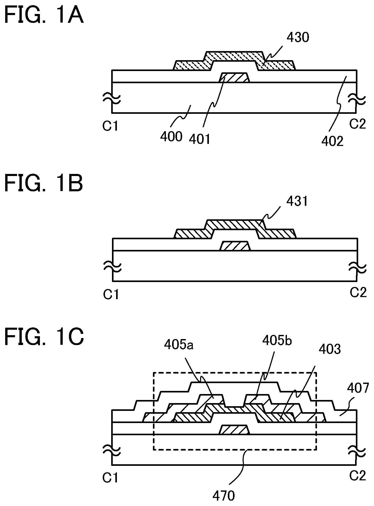
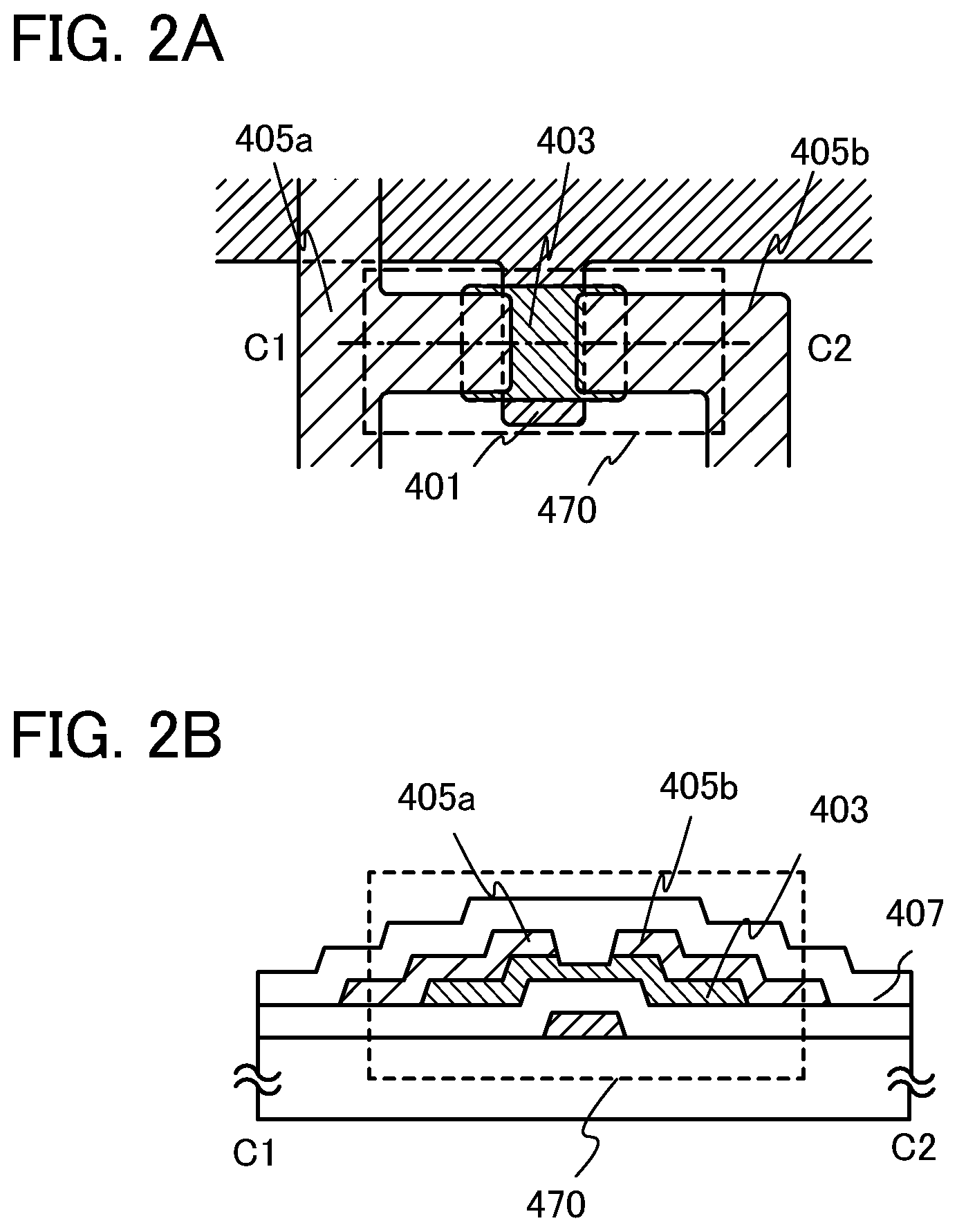
[0003] Note that as a method for providing a metal auxiliary wiring for a transparent electrode of an electro-optical element, a method by which the metal auxiliary wiring is provided so as to overlap with an upper surface of the transparent electrode or a lower surface of the transparent electrode and to be electrically connected to the transparent electrode has been known (for example, see Patent Document 1).
[0004] A structure in which an additional capacitor electrode provided for an active matrix substrate is formed of a conductive film having a light transmitting property of ITO, SnO.sub.2, or the like and an auxiliary wiring formed of a metal film is provided in contact with the additional capacitor electrode in order to reduce the electric resistance of the additional capacitor electrode has been known (see Patent Document 2).
[0005] Note that it has been known that, as each of a gate electrode, a source electrode, and a drain electrode of a field effect transistor formed using an amorphous oxide semiconductor film, a transparent electrode of indium tin oxide (ITO), indium zinc oxide, ZnO, SnO.sub.2, or the like, a metal electrode of Al, Ag, Cr, Ni, Mo, Au, Ti, Ta, or the like, or a metal electrode of an alloy containing any of the above elements can be used; and, by stacking two or more of these layers, contact resistance may be reduced or interface intensity may be improved (for example, see Patent Document 3).
[0006] Note that it has been known that, as a material of each of a source electrode, a drain electrode, a gate electrode and an auxiliary capacitor electrode of a transistor formed using an amorphous oxide semiconductor, a metal such as indium (In), aluminum (Al), gold (Au), or silver (Ag), or an oxide material such as indium oxide (In.sub.2O.sub.3), tin oxide (SnO.sub.2), zinc oxide (ZnO), cadmium oxide (CdO), cadmium indium oxide (CdIn.sub.2O.sub.4), cadmium tin oxide (Cd.sub.2SnO.sub.4), or zinc tin oxide (Zn.sub.2SnO.sub.4) can be used; and the same material or different materials may be used for the gate electrode, the source electrode, and the drain electrode (for example, see Patent Documents 4 and 5).
REFERENCE
[0007] [Patent Document 1] Japanese Published Patent Application No. H02-82221 [Patent Document 2] Japanese Published Patent Application No. H02-310536
[Patent Document 3] Japanese Published Patent Application No. 2008-243928
[Patent Document 4] Japanese Published Patent Application No. 2007-109918
[Patent Document 5] Japanese Published Patent Application No. 2007-115807
DISCLOSURE OF INVENTION
[0008] However, since a conductive film having a light transmitting property is used just for an electrode material in a conventional display panel which uses an oxide semiconductor, an aperture ratio cannot be improved. In addition, when a display device is manufactured using metal oxide, its reliability has not been taken into consideration.
[0009] In view of the above, an object of one embodiment of the present invention is to improve both the aperture ratio and reliability of a display device formed using metal oxide.
[0010] In a manufacturing method of a semiconductor device having a thin film transistor in which a semiconductor layer including a channel formation region is formed using an oxide semiconductor film, a heat treatment for reducing moisture and the like which are impurities and for improving the purity of the oxide semiconductor film (a heat treatment for dehydration or dehydrogenation) is performed. Further, impurities such as moisture existing not only in the oxide semiconductor film but also in a gate insulating layer and at interfaces between the oxide semiconductor film and a film above and in contact therewith and between the oxide semiconductor film and a film below and in contact therewith are reduced.
[0011] One embodiment of the present invention disclosed in this specification is a manufacturing method of a semiconductor device which includes the steps of: forming a gate electrode layer including metal oxide over a substrate having an insulating surface; forming a gate insulating layer over the gate electrode layer; forming an oxide semiconductor layer over the gate insulating layer; dehydrating or dehydrogenating the oxide semiconductor layer; forming a source electrode layer and a drain electrode layer including metal oxide over the dehydrated or dehydrogenated oxide semiconductor layer; forming a protective insulating layer in contact with part of the oxide semiconductor layer, over the gate insulating layer, the oxide semiconductor layer, the source electrode layer, and the drain electrode layer; and forming a pixel electrode layer including metal oxide over the protective insulating layer.
[0012] For dehydration or dehydrogenation, a heat treatment is performed in an oxygen atmosphere, in an inert gas atmosphere such as nitrogen or a rare gas (argon, helium, or the like), or under a reduced pressure at a temperature greater than or equal to 350.degree. C. or preferably greater than or equal to 400.degree. C. and less than the strain point of the substrate, whereby an impurity such as moisture contained in the oxide semiconductor layer is reduced.
[0013] Dehydration or dehydrogenation of the oxide semiconductor is conducted with conditions of the heat treatment such that at least a peak at around 300.degree. C. of two peaks of water are/is not detected when the dehydrated or dehydrogenated oxide semiconductor layer is measured with thermal desorption spectroscopy (TDS) while the temperature is increased to 450.degree. C. Therefore, even when a thin film transistor using the dehydrated or dehydrogenated oxide semiconductor layer is subjected to TDS at a temperature as high as 450.degree. C., at least a peak of water at around 300.degree. C. is not detected.
[0014] Then, slow cooling is performed from the heating temperature T at which the oxide semiconductor layer is dehydrated or dehydrogenated to a temperature low enough to prevent water from coming in again, specifically to a temperature which is more than 100.degree. C. lower than the heating temperature T, or more preferably to a temperature less than or equal to 100.degree. C.
[0015] A gas atmosphere in which the heating temperature T is decreased may be switched to a gas atmosphere different from that in which the temperature is increased to the heating temperature T.
[0016] Electric characteristics of a thin film transistor are improved and a thin film transistor having mass productivity and high performance is realized, by using an oxide semiconductor film which is formed by reducing moisture contained in the film by the heat treatment for dehydration or dehydrogenation and then subjected to slow cooling (or cooling) in an atmosphere containing no moisture (the dew point temperature of which is less than or equal to -40.degree. C. or preferably, less than or equal to -60.degree. C.).
[0017] In this specification, a heat treatment in an oxygen atmosphere, in an inert gas atmosphere such as nitrogen or a rare gas (argon, helium, or the like), or under a reduced pressure is called a heat treatment for dehydration or dehydrogenation. For convenience, dehydration or dehydrogenation in this specification refers to not only elimination of H.sub.2 by a heat treatment but also elimination of H, OH, or the like by a heat treatment.
[0018] In the case where a heat treatment is performed in an inert gas atmosphere such as nitrogen or a rare gas (argon, helium, or the like) or under a reduced pressure, it can be said that: an oxide semiconductor layer which has been of an i-type becomes an oxygen deficiency type layer and has low resistance by the heat treatment, i.e., becomes an n-type (such as n.sup.- or n.sup.+); and then, by forming an oxide insulating film in contact with the oxide semiconductor layer, the oxide semiconductor layer is placed into a state where oxygen is in excess so as to have a higher resistance, i.e., becomes an i-type. Thus, a semiconductor device including a thin film transistor which has favorable electric characteristics and high reliability can be manufactured and provided.
[0019] In the case where the heat treatment is performed in an inert gas atmosphere such as nitrogen or a rare gas (argon, helium, or the like) or under a reduced pressure, and then the atmosphere is switched to an oxygen atmosphere so that slow cooling is performed, an oxide semiconductor layer which has been of an i-type becomes an oxygen deficiency type layer and has low resistance by the heat treatment, i.e., becomes an n-type (such as n.sup.- or n.sup.+), and then, the oxide semiconductor layer is placed into a state where oxygen is in excess by the slow cooling in the oxygen atmosphere so as to have a higher resistance, i.e., becomes an i-type.
[0020] In addition, in the case where the heat treatment for dehydration or dehydrogenation is performed in an oxygen atmosphere, moisture in the oxide semiconductor layer is released, whereby the oxide semiconductor layer can be placed into a state where oxygen is in excess.
[0021] The term "oxide semiconductor" used in this specification is represented by InMO.sub.3(ZnO).sub.m (m>0), and a thin film transistor in which the thin film of the oxide semiconductor is used as an oxide semiconductor layer is manufactured. Note that M represents one or more metal elements selected from Ga, Fe, Ni, Mn, and Co. As an example, M may be Ga or may include the above metal element in addition to Ga; for example, M may be Ga and Ni or may be Ga and Fe. Moreover, in the above oxide semiconductor, in some cases, a transition metal element such as Fe or Ni or an oxide of the transition metal is contained as an impurity element in addition to a metal element contained as M. In this specification, among the oxide semiconductor whose structures are expressed by InMO.sub.3 (ZnO).sub.m (m>0), an oxide semiconductor which includes Ga as M is referred to as an In--Ga--Zn--O-based oxide semiconductor and a thin film of the In--Ga--Zn--O-based oxide semiconductor is referred to as an In--Ga--Zn--O-based non-single-crystal film.
[0022] As the metal oxide applied to the oxide semiconductor layer, any of the following metal oxide can be applied besides the above: an In--Sn--Zn--O-based metal oxide; an In--Al--Zn--O-based metal oxide; a Sn--Ga--Zn--O-based metal oxide; an Al--Ga--Zn--O-based metal oxide; a Sn--Al--Zn--O-based metal oxide; an In--Zn--O-based metal oxide; a Sn--Zn--O-based metal oxide; an Al--Zn--O-based metal oxide; an In--O-based metal oxide; a Sn--O-based metal oxide; and a Zn--O-based metal oxide. Alternatively, the silicon oxide may be included in the oxide semiconductor layer formed using the above metal oxide.
[0023] The oxide semiconductor preferably includes In, or more preferably, In and Ga. Dehydration or dehydrogenation is effective in changing the oxide semiconductor layer into an i-type (intrinsic).
[0024] In the case where the heat treatment for dehydration or dehydrogenation is performed after the oxide semiconductor layer is formed, the oxide semiconductor layer which is amorphous is changed into a microcrystalline film or a polycrystalline film in some cases depending on the condition of the heat treatment or the material of the oxide semiconductor layer. Further, the oxide semiconductor layer is partially crystallized in some cases; for example, crystal grains (nanocrystals) may be included in the amorphous structure. Even when the oxide semiconductor layer is changed into a microcrystalline film or a polycrystalline film, the thin film transistor can obtain switching characteristics as long as the oxide semiconductor layer is placed into a state where oxygen is in excess to have a higher resistance, i.e., to become an i-type.
[0025] However, the oxide semiconductor layer is preferably amorphous in order to reduce off-current of the TFT and to achieve low power consumption.
[0026] In order to be amorphous even after the heat treatment for dehydration or dehydrogenation which follows the formation of the oxide semiconductor layer, the oxide semiconductor layer preferably has a small thickness of less than or equal to 50 nm. By making the thickness of the oxide semiconductor layer small, crystallization in the oxide semiconductor layer at the time of the heat treatment after the formation thereof can be suppressed.
[0027] Alternatively, in order to be amorphous even after the heat treatment for dehydration or dehydrogenation which follows the formation of the oxide semiconductor layer, the oxide semiconductor layer is made to include silicon oxide (SiO.sub.x (X>0)) which inhibits crystallization, and thus can be prevented from being crystallized when the heat treatment is performed after the oxide semiconductor layer is formed in the manufacturing process.
[0028] Note that in this specification, off current is current which flows between a source electrode and a drain electrode when a transistor is in an off state. For example, in an n-channel transistor, the off current is current which flows between a source electrode and a drain electrode when gate voltage is lower than threshold voltage of the transistor.
[0029] Further, a gate electrode layer, a source electrode layer, a drain electrode layer, a pixel electrode layer, another electrode layer, or another wiring layer can be formed by a sputtering method, a vacuum evaporation method (such as an electron beam evaporation method), an arc discharge ion plating method or a spray method using a conductive material having a visible light transmitting property such as the following metal oxide: an In--Sn--Zn--O-based metal oxide; an In--Al--Zn--O-based metal oxide; a Sn--Ga--Zn--O-based metal oxide; an Al--Ga--Zn--O-based metal oxide; a Sn--Al--Zn--O-based metal oxide; an In--Zn--O-based metal oxide; a Sn--Zn--O-based metal oxide; an Al--Zn--O-based metal oxide; an In--O-based metal oxide; a Sn--O-based metal oxide; and a Zn--O-based metal oxide. Further, the silicon oxide may be included in a wiring layer or an electrode layer which is formed of the above metal oxide.
[0030] As other materials which may be used for the gate electrode layer, the source electrode layer, the drain electrode layer, the pixel electrode layer, another electrode layer, or another wiring layer, an Al--Zn--O-based non-single-crystal film including nitrogen, which is an Al--Zn--O--N-based non-single-crystal film, a Zn--O--N-based non-single-crystal film including nitrogen, or a Sn--Zn--O--N-based non-single-crystal film including nitrogen may be used. Note that the relative proportion (atomic %) of zinc in an Al--Zn--O--N-based oxide semiconductor film is less than or equal to 47 atomic % and is larger than the relative proportion (atomic %) of aluminum in the oxide semiconductor film. The relative proportion (atomic %) of aluminum in the oxide semiconductor film is larger than the relative proportion (atomic %) of nitrogen in a conductive film having a light transmitting property. Note that the unit of the relative proportion in the conductive film having a light transmitting property is atomic percent, and the relative proportion is evaluated by analysis using an electron probe X-ray microanalyzer (EPMA).
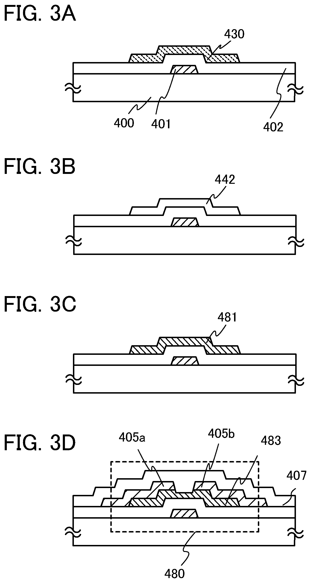
[0031] An aperture ratio of a display device can be improved by using a conductive film having a visible light transmitting property for the gate electrode layer, the source electrode layer, the drain electrode layer, the pixel electrode layer, another electrode layer, or another wiring layer. In addition, when a material having a light transmitting property is used also for the oxide semiconductor layer, the aperture ratio can be further improved. By using a film having a light transmitting property for components (a wiring and a semiconductor layer) of a thin film transistor, particularly in a small liquid crystal display device, a high aperture ratio can be achieved even when the size of a pixel is miniaturized for an increase in the number of scan lines, for example, so as to realize high definition of a display image. Further, by using a film having a light transmitting property for components of a thin film transistor, a high aperture ratio can be achieved even when one pixel is divided into a plurality of sub-pixels in order to realize a wide viewing angle. In other words, an aperture ratio can be high even when a group of thin film transistors is densely arranged and an area of a display region can be sufficiently secured. For example, in the case where one pixel includes two to four sub-pixels, an aperture ratio can be improved because not only the thin film transistor but also their respective storage capacitor has a light transmitting property.
[0032] Also in a light-emitting display device, a high aperture ratio can be achieved by using a film having a light transmitting property for components (a wiring and a semiconductor layer) of a thin film transistor even when a plurality of thin film transistors is placed in one pixel. In a light-emitting display device using a light-emitting element, a plurality of thin film transistors is included in a pixel portion, and a portion in which a gate electrode of a thin film transistor is electrically connected to a source wiring or a drain wiring of another transistor is also included in the pixel portion. For example, even when two to seven thin film transistors and a storage capacitor are included in one pixel in a light-emitting display device, a high aperture ratio can be achieved because the thin film transistors and the storage capacitor have a light transmitting property.
[0033] In addition, when the gate electrode layer, the source electrode layer, the drain electrode layer, the pixel electrode layer, another electrode layer, and another wiring layer are formed using the same material, a common sputtering target and a common manufacturing apparatus can be used; therefore, cost of the material of these layers and an etchant (or an etching gas) which is used in etching can be reduced, resulting in a reduction in manufacturing cost.
[0034] In this specification, a film having a visible light transmitting property refers to a film with a thickness which realizes a visible light transmittance of 75% to 100%. Such a film is referred to also as a transparent conductive film. A conductive film which is semitransparent to visible light may be used as metal oxide for the gate electrode layer, the source electrode layer, the drain electrode layer, the pixel electrode layer, another electrode layer, or another wiring layer. When a conductive film is semitransparent to visible light, it has a transmittance of visible light of 50% to 75%.
[0035] The thickness of each of the gate electrode layer, the source electrode layer, the drain electrode layer, the pixel electrode layer, another electrode layer, and another wiring layer is set to greater than or equal to 30 nm and less than or equal to 200 nm. A thickness which allows each layer to have a light transmitting property or to be semitransparent to visible light may be selected.
[0036] Further, the gate insulating layer and the oxide semiconductor film may be processed successively (also referred to as successive processing, in situ process, or successive formation) without exposure to air. When the gate insulating layer and the oxide semiconductor film are successively processed without exposure to air, the gate insulating layer and the oxide semiconductor film can be formed without contamination of an interface thereof by atmospheric components or impurity elements floating in air, such as moisture or hydrocarbon. Therefore, variation in characteristics between the thin film transistors can be reduced.
[0037] Note that the term "successive processing" in this specification means that during a series of a first treatment step by a PCVD method or a sputtering method to a second treatment step by a PCVD method or a sputtering method, an atmosphere in which a substrate to be processed is disposed is not contaminated by a contaminant atmosphere such as air, and is constantly controlled to be vacuum, an inert gas atmosphere (a nitrogen atmosphere or a rare gas atmosphere) or an oxygen atmosphere. By the successive processing, film formation or the like can be performed while preventing moisture or the like from attaching again to the substrate to be processed which is cleaned.
[0038] Performing the process from the first treatment step to the second treatment step in the same chamber is within the scope of the successive processing in this specification.
[0039] In addition, the following is also within the scope of the successive processing in this specification: in the case of performing the process from the first treatment step to the second treatment step in different chambers, the substrate is transferred after the first treatment step to another chamber without being exposed to air and subjected to the second treatment.
[0040] Note that between the first treatment step and the second treatment step, a substrate transfer step, an alignment step, a slow-cooling step, a step of heating or cooling the substrate to a temperature which is necessary for the second step or the like may be provided. Such a process is also within the scope of the successive processing in this specification.
[0041] A step in which liquid is used, such as a cleaning step, wet etching, or resist formation, may be provided between the first treatment step and the second treatment step. This case is not within the scope of the successive treatment in this specification.
[0042] A semiconductor device having a structure which is obtained by the above manufacturing method is a semiconductor device including: a gate electrode layer over a substrate having an insulating surface; a gate insulating layer over the gate electrode layer; an oxide semiconductor layer over the gate insulating layer; a source electrode layer and a drain electrode layer over the oxide semiconductor layer; a protective insulating layer in contact with part of the oxide semiconductor layer, over the gate insulating layer, the oxide semiconductor layer, the source electrode layer, and the drain electrode layer; and a pixel electrode layer including metal oxide over the protective insulating layer. In the above structure, the gate electrode layer, the gate insulating layer, the oxide semiconductor layer, the source electrode layer, the drain electrode layer, the protective insulating layer, and the pixel electrode layer have a light transmitting property. The pixel electrode layer overlaps with the oxide semiconductor layer and the gate electrode layer.
[0043] With the above structure, at least one of the above problems is resolved.
[0044] In the above structure, although the pixel electrode layer overlaps with the oxide semiconductor layer and the gate electrode layer, the overlapping region can also serve as a display region, whereby a high aperture ratio can be realized. The pixel electrode layer which overlaps with the oxide semiconductor layer and the gate electrode layer may be a pixel electrode layer of an adjacent pixel. In other words, a structure can be employed in which the pixel electrode layer electrically connected to the oxide semiconductor layer with the source electrode layer and the drain electrode layer therebetween overlaps not with the channel formation region of the oxide semiconductor layer but with the pixel electrode layer of an adjacent pixel.
[0045] In a terminal portion in which a plurality of terminal electrodes connected to an external terminal such as an FPC is placed, the terminal electrodes can be formed using the same material and process as the gate electrode layer, the source electrode layer, the drain electrode layer, or the pixel electrode layer.
[0046] Further, the storage capacitors in the pixel portion of the liquid crystal display device or the light-emitting display device include a capacitor wiring layer which is formed of a conductive material having a visible light transmitting property, a capacitor electrode layer which is formed of a conductive material having a visible light transmitting property, and the gate insulating layer that is used as a dielectric. Note that the capacitor wiring layer in this case can be formed using the same material and process as the gate electrode layer. In addition, the capacitor electrode layer can be formed using the same material and process as the source electrode layer or the drain electrode layer.
[0047] Alternatively, the storage capacitors in the pixel portion of the liquid crystal display device or the light-emitting display device may include a capacitor wiring layer formed of a conductive material having a visible light transmitting property, a pixel electrode layer which is formed of a conductive material having a visible light transmitting property, and the protective insulating layer that is used as a dielectric. The capacitor wiring layer in this case can be formed using the same material and process as the source electrode layer or the drain electrode layer.
[0048] Moreover, as a display device including a thin film transistor, a light-emitting display device in which a light-emitting element is used and a display device in which an electrophoretic display element is used, which is also referred to as electronic paper, are given in addition to a liquid crystal display device.
[0049] There is no particular limitation on the foregoing liquid crystal display device, and a liquid crystal display device using TN liquid crystal, IPS liquid crystal, OCB liquid crystal, STN liquid crystal, VA liquid crystal, ECB liquid crystal, GH liquid crystal, polymer dispersed liquid crystal, discotic liquid crystal, or the like can be used. Among them, a normally black liquid crystal panel, such as a transmissive liquid crystal display device utilizing a vertical alignment (VA) mode is preferable. Some examples are given as a vertical alignment mode. For example, an MVA (multi-domain vertical alignment) mode, a PVA (patterned vertical alignment) mode, an ASV mode, or the like can be employed. Specifically, one pixel is divided into a plurality of sub-pixels and a projection portion is provided in a position of a counter substrate corresponding to the center of each sub-pixel, so that a multi-domain pixel is formed. Such a driving method, in which one pixel is divided into a plurality of sub-pixels and a projection portion is provided at a position of a counter substrate which corresponds to the center of each sub-pixel so that orientation division (multi-domain) of one pixel is performed and a wide viewing angle is achieved, is referred to as sub-pixel driving. It is to be noted that the projection portion may be provided over/on either one or both of the counter substrate and the element substrate. The projection portion makes liquid crystal molecules orient radially and improves controllability of the orientation.
[0050] Further, an electrode for driving liquid crystal, that is, a pixel electrode may have a top view shape like a comb-shape or a zigzagged shape so that a direction in which voltage is applied may be varied. Further, a multi-domain pixel may be formed utilizing photo-alignment.
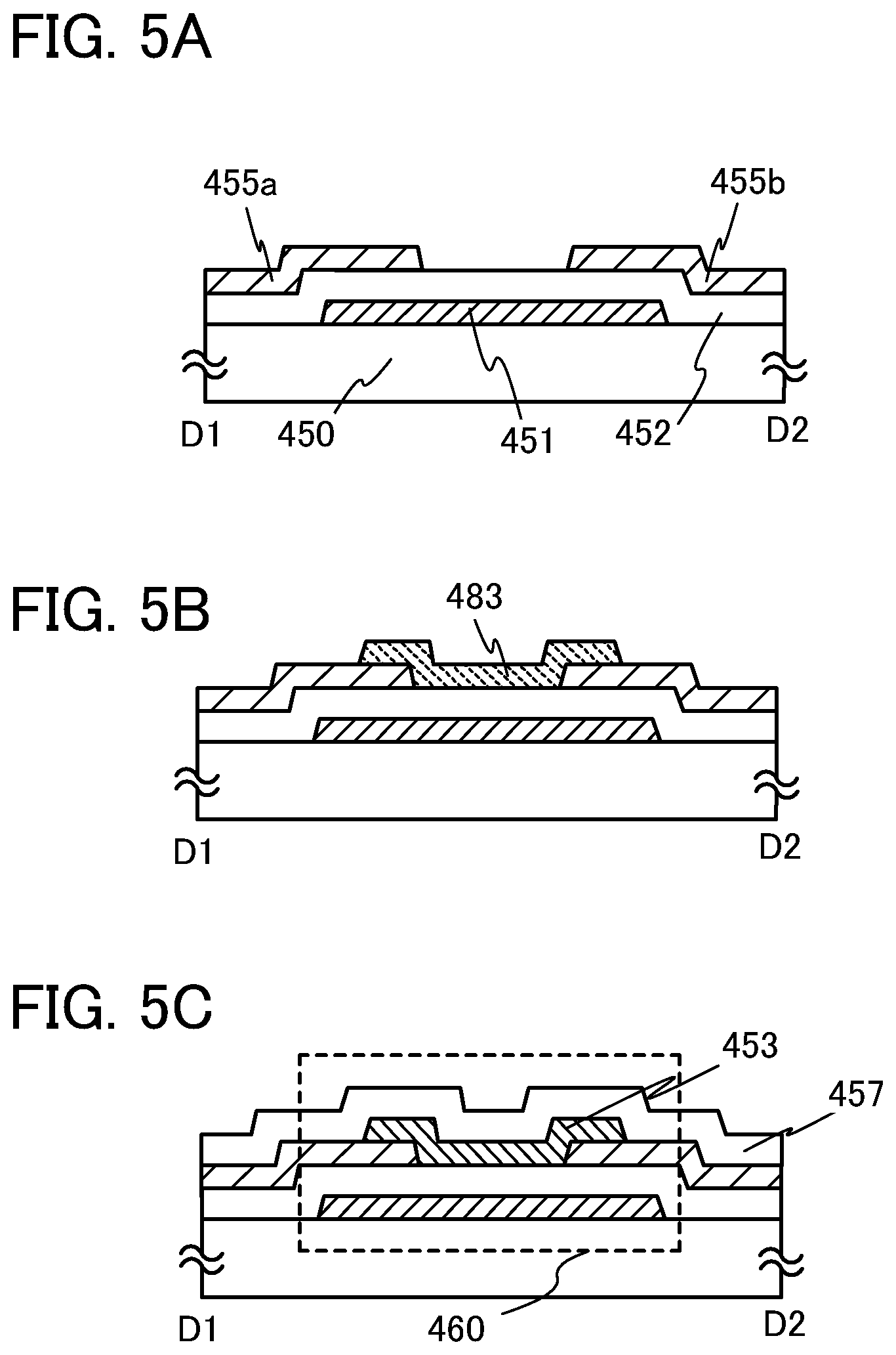
[0051] Since a thin film transistor is easily broken due to static electricity or the like, a protective circuit for protecting the thin film transistor in the pixel portion is preferably provided over the same substrate for a gate line or a source line. The protective circuit is preferably formed with a non-linear element including an oxide semiconductor.
[0052] In a pixel portion of a display device, by using a film having a light transmitting property for components of a thin film transistor, a high aperture ratio can be achieved even when the size of a pixel is miniaturized for an increase in the number of scan lines, for example, so as to realize high definition of a display image. Further, by using a film having a light transmitting property for components of a thin film transistor, a high aperture ratio can be achieved even when one pixel is divided into a plurality of sub-pixels in order to realize a wide viewing angle.
BRIEF DESCRIPTION OF DRAWINGS
[0053] In the accompanying drawings:
[0054] FIGS. 1A to 1C are cross-sectional views illustrating manufacturing steps of one embodiment of the present invention;
[0055] FIGS. 2A and 2B are a plan view and a cross-sectional view, respectively, illustrating one embodiment of the present invention;
[0056] FIGS. 3A to 3D are cross-sectional views illustrating manufacturing steps of one embodiment of the present invention;
[0057] FIGS. 4A to 4C are cross-sectional views illustrating manufacturing steps of one embodiment of the present invention;
[0058] FIGS. 5A to 5C are cross-sectional views illustrating manufacturing steps of one embodiment of the present invention;
[0059] FIGS. 6A and 6B are a plan view and a cross-sectional view, respectively, illustrating one embodiment of the present invention;
[0060] FIGS. 7A and 7B are cross-sectional views illustrating manufacturing steps of one embodiment of the present invention, and FIG. 7C is a plan view illustrating one embodiment of the present invention;
[0061] FIGS. 8A to 8D are cross-sectional views illustrating manufacturing steps of one embodiment of the present invention;
[0062] FIGS. 9A to 9C are cross-sectional views illustrating manufacturing steps of one embodiment of the present invention;
[0063] FIG. 10 is a plan view illustrating one embodiment of the present invention;
[0064] FIG. 11 is a plan view illustrating one embodiment of the present invention;
[0065] FIGS. 12A and 12C are cross-sectional views and FIGS. 12B and 12D are plan views illustrating one embodiment of the present invention;
[0066] FIGS. 13A to 13C are perspective views illustrating one embodiment of the present invention;
[0067] FIGS. 14A and 14B are block diagrams illustrating one embodiment of the present invention;
[0068] FIG. 15 is a timing chart illustrating one embodiment of the present invention;
[0069] FIG. 16 is an equivalent circuit diagram of a pixel in a semiconductor device;
[0070] FIGS. 17A to 17C are cross-sectional views each illustrating a semiconductor device;
[0071] FIGS. 18A and 18B are diagrams each illustrating a semiconductor device;
[0072] FIGS. 19A and 19B are diagrams each illustrating a semiconductor device; and
[0073] FIG. 20 is a diagram illustrating a semiconductor device.
BEST MODE FOR CARRYING OUT THE INVENTION
[0074] Hereinafter, embodiments of the present invention will be described in detail with reference to the accompanying drawings. However, the present invention is not limited to the description below, and it is easily understood by those skilled in the art that modes and details disclosed herein can be modified in various ways. Therefore, the present invention is not construed as being limited to description of the embodiments.
Embodiment 1
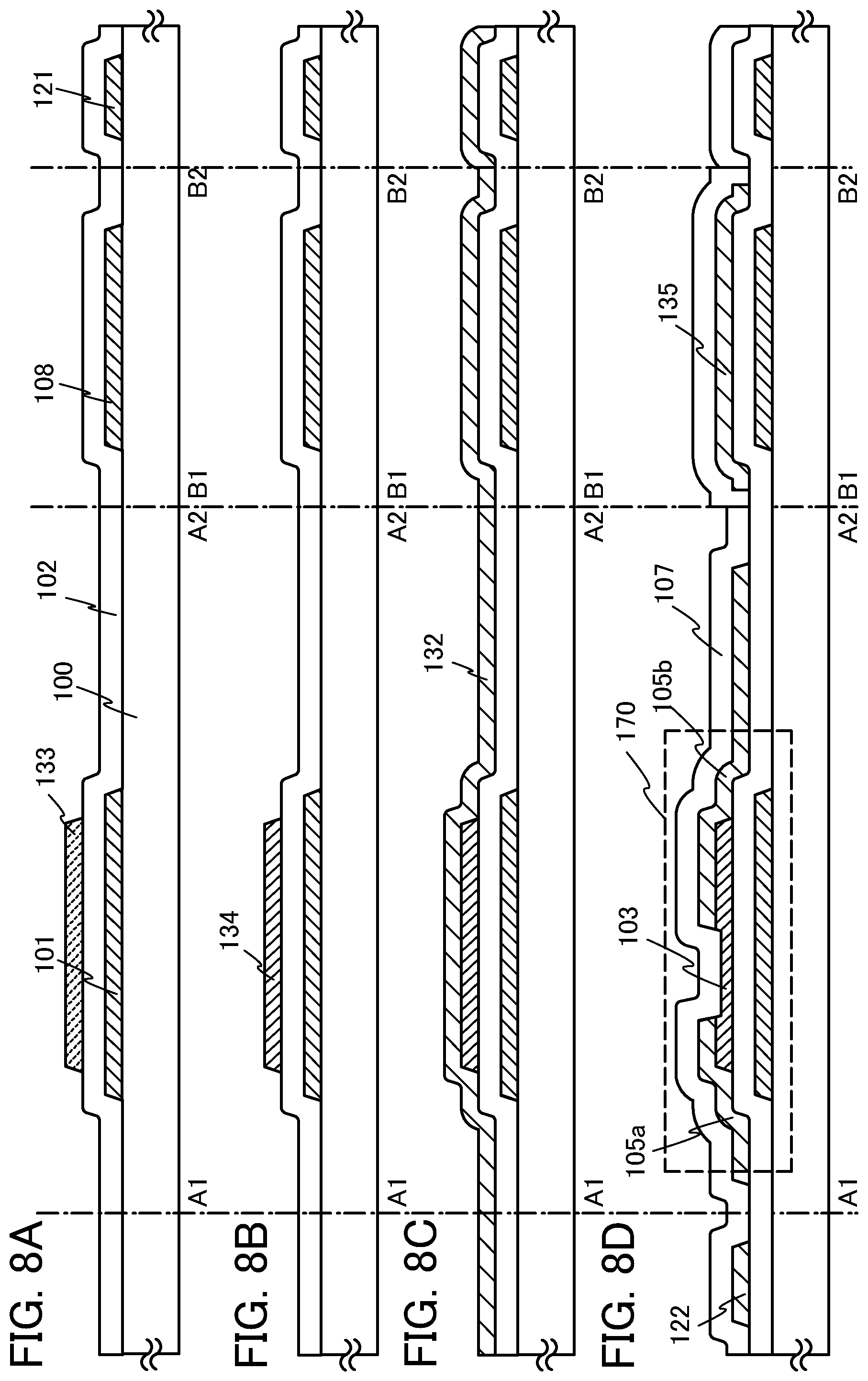
[0075] A semiconductor device and a method for manufacturing a semiconductor device will be described with reference to FIGS. 1A to 1C and FIGS. 2A and 2B. In FIG. 2B, a thin film transistor 470 which is one type of a structure called a channel-etch type is illustrated.
[0076] FIG. 2A is a plan view of the thin film transistor 470 included in a semiconductor device, and FIG. 2B is a cross-sectional view taken along line C1-C2 of FIG. 2A. The thin film transistor 470 is a bottom gate thin film transistor and includes, over a substrate 400 having an insulating surface, a gate electrode layer 401, a gate insulating layer 402, an oxide semiconductor layer 403, a source electrode layer 405a, and a drain electrode layer 405b. In addition, an oxide insulating film 407 is provided to cover the thin film transistor 470 and be in contact with the oxide semiconductor layer 403.
[0077] The substrate 400 having an insulating surface, the gate electrode layer 401, the gate insulating layer 402, the oxide semiconductor layer 403, the source electrode layer 405a, the drain electrode layer 405b, and the oxide insulating film 407 are all formed using a material having a visible light transmitting property. Thus, the thin film transistor 470 has a light transmitting property and an aperture ratio can be improved in the case where the thin film transistor 470 is placed in a pixel portion of a display device.
[0078] As for the oxide semiconductor layer 403, at least after an oxide semiconductor film is formed, a heat treatment (a heat treatment for dehydration or dehydrogenation) for reducing moisture and the like which are impurities is performed. The heat treatment for dehydration or dehydrogenation and slow cooling follow the formation of an oxide insulating film in contact with the oxide semiconductor layer, and the like; accordingly, the carrier of the oxide semiconductor layer is reduced to lead to an improvement in the reliability of the thin film transistor 470.
[0079] Impurities such as moisture are reduced not only in the oxide semiconductor layer 403 but also in the gate insulating layer 402, at interfaces between the oxide semiconductor layer 403 and a film above and in contact therewith and between the oxide semiconductor layer 403 and a film below and in contact therewith which are specifically an interface between the gate insulating layer 402 and the oxide semiconductor layer 403 and an interface between the oxide insulating film 407 and the oxide semiconductor layer 403.
[0080] Hereinafter, cross-sectional views which describe the manufacturing process of the thin film transistor 470 illustrated in FIG. 2B are in FIGS. 1A to 1C.
[0081] In FIG. 1A, the gate electrode layer 401 is provided over the substrate 400 having an insulating surface.
[0082] Although there is no particular limitation on a substrate which can be used as the substrate 400 having an insulating surface, it is necessary that the substrate have at least enough heat resistance to a heat treatment to be performed later. As the substrate 400 having an insulating surface, a glass substrate formed of barium borosilicate glass, aluminoborosilicate glass, or the like can be used.
[0083] In the case where a glass substrate is used and the temperature at which the heat treatment is to be performed later is high, a glass substrate whose strain point is greater than or equal to 730.degree. C. is preferably used. As a glass substrate, a glass material such as aluminosilicate glass, aluminoborosilicate glass, or barium borosilicate glass is used, for example. Note that by containing a larger amount of barium oxide (BaO) than boric acid, a glass substrate is heat-resistant and of more practical use. Therefore, a glass substrate containing BaO and B.sub.2O.sub.3 so that the amount of BaO is larger than that of B.sub.2O.sub.3 is preferably used.
[0084] Note that a substrate formed of an insulator such as a ceramic substrate, a quartz substrate, or a sapphire substrate may be used instead of the above glass substrate. Alternatively, crystallized glass or the like can be used.
[0085] Further, an insulating film serving as a base film may be provided between the substrate 400 and the gate electrode layer 401. The base film has a function of preventing diffusion of an impurity element from the substrate 400, and can be formed to have a single-layer or stacked-layer structure using one or more of a silicon nitride film, a silicon oxide film, a silicon nitride oxide film, and a silicon oxynitride film.
[0086] As the material of the gate electrode layer 401, a conductive material having a visible light transmitting property such as the following materials can be employed: an In--Sn--Zn--O-based metal oxide; an In--Al--Zn--O-based metal oxide; a Sn--Ga--Zn--O-based metal oxide; an Al--Ga--Zn--O-based metal oxide; a Sn--Al--Zn--O-based metal oxide; an In--Zn--O-based metal oxide; a Sn--Zn--O-based metal oxide; an Al--Zn--O-based metal oxide; an In--O-based metal oxide; a Sn--O-based metal oxide; and a Zn--O-based metal oxide. The thickness of the gate electrode layer 401 is selected as appropriate to be within the range of 30 nm to 200 nm. As a deposition method of the metal oxide used for the gate electrode layer 401, a sputtering method, a vacuum evaporation method (an electron beam evaporation method or the like), an arc discharge ion plating method or a spray method is used.
[0087] Next, the gate insulating layer 402 is formed over the gate electrode layer 401.
[0088] The gate insulating layer 402 can be formed to have a single-layer or stacked layer structure using a silicon oxide layer, a silicon nitride layer, a silicon oxynitride layer, or a silicon nitride oxide layer by a plasma CVD method, a sputtering method, or the like. For example, a silicon oxynitride layer may be formed using SiH.sub.4, oxygen, and nitrogen as a film formation gas by a plasma CVD method.
[0089] Then, an oxide semiconductor film is formed to a thickness of greater than or equal to 2 nm and less than or equal to 200 nm over the gate insulating layer 402.
[0090] Note that before the oxide semiconductor film is formed by a sputtering method, dust on a surface of the gate insulating layer 402 is preferably removed by reverse sputtering in which an argon gas is introduced and plasma is generated. The reverse sputtering refers to a method in which, without application of a voltage to a target side, an RF power source is used for application of a voltage to a substrate side in an argon atmosphere to generate plasma in the vicinity of the substrate to modify a surface. Note that instead of argon, nitrogen, helium, oxygen or the like may be used.
[0091] The oxide semiconductor film is formed by a sputtering method with use of an In--Ga--Zn--O-based oxide semiconductor target. Alternatively, the oxide semiconductor film can be formed by a sputtering method in a rare gas (typically argon) atmosphere, in an oxygen atmosphere, or in an atmosphere including a rare gas (typically argon) and oxygen.
[0092] The gate insulating layer 402 and the oxide semiconductor film may be formed successively without exposure to air. When the gate insulating layer 402 and the oxide semiconductor film are successively formed without exposure to air, the gate insulating layer 402 and the oxide semiconductor film can be formed without contamination of an interface thereof by atmospheric components or impurity elements floating in air, such as moisture or hydrocarbon. Therefore, variation in characteristics between the thin film transistors can be reduced.
[0093] Then, the oxide semiconductor film is processed into an oxide semiconductor layer (a first oxide semiconductor layer 430), which is an island-shaped oxide semiconductor layer, by a photolithography step (see FIG. 1A).
[0094] Next, the first oxide semiconductor layer 430 is dehydrated or dehydrogenated. A temperature at which a first heat treatment for dehydration or dehydrogenation is performed is greater than or equal to 350.degree. C. and less than the strain point of the substrate, preferably greater than or equal to 400.degree. C. Here, the substrate is introduced into an electric furnace which is one of heat treatment apparatuses and the first oxide semiconductor layer 430 is subjected to a heat treatment in an oxygen atmosphere; then, the slow cooling is performed in the oxygen atmosphere, whereby a second oxide semiconductor layer 431 is formed (see FIG. 1B). The slow cooling is performed from the heating temperature T at which the oxide semiconductor layer is dehydrated or dehydrogenated to a temperature low enough to prevent water from coming in again, specifically to a temperature which is more than 100.degree. C. lower than the heating temperature T. Alternatively, the slow cooling is performed to a temperature lower than a temperature of a second heat treatment which is to be performed later and then the substrate is taken out of the heat treatment apparatus. The oxide semiconductor layer is subjected to the heat treatment in the oxygen atmosphere, whereby an impurity such as water contained in the oxide semiconductor layer can be removed and at the same time, the second oxide semiconductor layer 431 is placed into a state where oxygen is in excess. The oxide semiconductor layer is crystallized and changed into a microcrystalline film or a polycrystalline film in some cases depending on the condition of the first heat treatment or the material of the oxide semiconductor layer.
[0095] Note that in the first heat treatment, it is preferable that water, hydrogen, and the like be not contained in the oxygen gas. Alternatively, the purity of the oxygen gas which is introduced into the heat treatment apparatus is preferably greater than or equal to 6N (99.9999%) or more preferably greater than or equal to 7N (99.99999%) (that is, the impurity concentration in the oxygen is less than or equal to 1 ppm, or preferably less than or equal to 0.1 ppm).
[0096] The first heat treatment is performed for greater than or equal to 0.5 hours and less than or equal to 10 hours, where the rate of temperature increase of the electric furnace is preferably greater than or equal to 0.1.degree. C./min and less than or equal to 20.degree. C./min. Further, the rate of temperature decrease in the electric furnace is preferably greater than or equal to 0.1.degree. C./min and less than or equal to 15.degree. C./min.
[0097] As a result, the reliability of the thin film transistor to be formed later can be improved.
[0098] Further, instead of the heating method in which an electric furnace is used, a rapid heating method such as a gas rapid thermal anneal (GRTA) method using a heated gas or a lamp rapid thermal anneal (LRTA) method using lamp light can be used for the first heat treatment.
[0099] In the case where the heat treatment apparatus is a multi-chamber type, a chamber for the first heat treatment can be different from that for a cooling treatment. Typically, the oxide semiconductor layer over the substrate is heated in a first chamber which is filled with an oxygen gas and whose temperature is increased to greater than or equal to 400.degree. C. and less than the strain point of the substrate. Then, through a transfer chamber into which an oxygen gas is introduced, the substrate on which the above first heat treatment is performed is transferred into a second chamber which is filled with oxygen and whose temperature is less than or equal to 100.degree. C. or preferably room temperature, and is subjected to the cooling treatment. Through the above steps, throughput can be improved.
[0100] Alternatively, the oxide semiconductor film before being processed into the island-shaped oxide semiconductor layer can also be subjected to the first heat treatment in an oxygen atmosphere. In that case, after the first heat treatment and the cooling treatment of the oxide semiconductor film, the substrate is taken out of the heating device and a photolithography step is performed.
[0101] Before the oxide semiconductor film is formed, the gate insulating layer may be subjected to a heat treatment (at a temperature greater than or equal to 400.degree. C. and less than the strain point of the substrate) in an inert gas (nitrogen or a rare gas such as helium, neon, or argon) atmosphere, in an oxygen atmosphere, or under a reduced pressure so that an impurity such as hydrogen and water in the layer is removed.
[0102] Next, a conductive film is formed over the gate insulating layer 402 and the second oxide semiconductor layer 431. As a deposition method of the conductive film, a sputtering method, a vacuum evaporation method (an electron beam evaporation method or the like), an arc discharge ion plating method, or a spray method is used.
[0103] As the material of the conductive film, a conductive material having a visible light transmitting property such as the following materials can be employed: an In--Sn--Zn--O-based metal oxide; an In--Al--Zn--O-based metal oxide; a Sn--Ga--Zn--O-based metal oxide; an Al--Ga--Zn--O-based metal oxide; a Sn--Al--Zn--O-based metal oxide; an In--Zn--O-based metal oxide; a Sn--Zn--O-based metal oxide; an Al--Zn--O-based metal oxide; an In--O-based metal oxide; a Sn--O-based metal oxide; and a Zn--O-based metal oxide. The thickness of the conductive film is selected as appropriate to be within the range of 30 nm to 200 nm.
[0104] Then, the second oxide semiconductor layer 431 and the conductive film are selectively etched by a photolithography step so as to form the oxide semiconductor layer 403, the source electrode layer 405a, and the drain electrode layer 405b. Note that only part of the oxide semiconductor layer is etched to be the oxide semiconductor layer having a groove (depression). When oxygen ashing is performed at the time of removing a resist mask which is used at this photolithography step, oxygen is introduced into an exposed region of the oxide semiconductor layer.
[0105] Next, the oxide insulating film 407 serving as a protective insulating layer is formed in contact with part of the oxide semiconductor layer 403, whereby the thin film transistor 470 can be manufactured (see FIG. 1C). The oxide insulating film 407 is formed to have a thickness of at least greater than or equal to 1 nm and can be appropriately formed by a method in which an impurity such as water or hydrogen is prevented from entering the oxide insulating film 407, for example, by a CVD method or a sputtering method. Here, the oxide insulating film 407 is formed by a sputtering method. The oxide insulating film 407, which is formed in contact with the low-resistance oxide semiconductor layer, does not contain an impurity such as moisture, a hydrogen ion, or OH.sup.- and is formed using an inorganic insulating film which prevents intrusion of these from the outside. Typically, a silicon oxide film, a silicon nitride oxide film, an aluminum oxide film, or an aluminum oxynitride film is used. Alternatively, a silicon nitride film or an aluminum nitride film on and in contact with the oxide insulating film 407 may be formed. The silicon nitride film does not contain an impurity such as moisture, a hydrogen ion, or OH.sup.- and prevents intrusion of these from the outside.
[0106] In this embodiment, a silicon oxide film with a thickness of 300 nm is formed as the oxide insulating film 407. A substrate temperature at the time of the film formation may be greater than or equal to room temperature and less than or equal to 300.degree. C.; in this embodiment, the substrate temperature is 100.degree. C. The silicon oxide film can be formed by a sputtering method in a rare gas (typically argon) atmosphere, in an oxygen atmosphere, or in an atmosphere including a rare gas (typically argon) and oxygen. As a target, a silicon oxide target or a silicon target can be used; for example, the silicon oxide film can be formed using a silicon target by a sputtering method in an atmosphere including oxygen and nitrogen.
[0107] Further, after the oxide insulating film 407 is formed, the thin film transistor 470 may be subjected to the second heat treatment (preferably at a temperature greater than or equal to 150.degree. C. and less than 350.degree. C.) in a nitrogen atmosphere or in an oxygen atmosphere. For example, the second heat treatment is performed in a nitrogen atmosphere at 250.degree. C. for one hour. By the second heat treatment, the oxide semiconductor layer 403 is heated while being in contact with the oxide insulating film 407; thus, variation in electric characteristics of the thin film transistor 470 can be reduced.
Embodiment 2
[0108] A semiconductor device and a method for manufacturing a semiconductor device which are different from Embodiment 1 will be described with reference to FIGS. 3A to 3D. The portion that is identical to or has a function similar to those described in Embodiment 1 can be formed in a manner similar to that described in Embodiment 1; therefore, repetitive description is omitted.
[0109] FIGS. 3A to 3D are cross-sectional views illustrating a manufacturing process of a thin film transistor 480. The structure of the thin film transistor 480 which is illustrated in FIG. 3D is called an inverted coplanar type (also called a bottom-contact type).
[0110] Similarly to Embodiment 1, the gate electrode layer 401 is provided over the substrate 400 having an insulating surface. An insulating film serving as a base film may be provided between the substrate 400 and the gate electrode layer 401.
[0111] Next, similarly to Embodiment 1, the gate insulating layer 402 is formed over the gate electrode layer 401. Then, an oxide semiconductor film is formed over the gate insulating layer 402.
[0112] The oxide semiconductor film is then processed into an oxide semiconductor layer (the first oxide semiconductor layer 430), which is an island-shaped oxide semiconductor layer, by a photolithography step (see FIG. 3A). Note that FIG. 3A is the same as FIG. 1A.
[0113] Next, the first oxide semiconductor layer 430 is dehydrated or dehydrogenated. A temperature at which a first heat treatment for dehydration or dehydrogenation is performed is greater than or equal to 350.degree. C. and less than the strain point of the substrate, preferably greater than or equal to 400.degree. C. Here, the substrate is introduced into an electric furnace which is one of heat treatment apparatuses and the first oxide semiconductor layer 430 is subjected to a heat treatment in an inert gas (nitrogen or a rare gas such as helium, neon, or argon) atmosphere or under a reduced pressure, whereby a second oxide semiconductor layer 442 is formed (see FIG. 3B). By the heat treatment in an inert gas atmosphere or under a reduced pressure, the resistance of the oxide semiconductor layer is reduced (a carrier concentration thereof is increased preferably to greater than or equal to 1.times.10.sup.18/cm.sup.3) and a low-resistance oxide semiconductor layer (the second oxide semiconductor layer 442) can be formed.
[0114] Note that in the first heat treatment, it is preferable that water, hydrogen, and the like be not contained in the nitrogen or the rare gas such as helium, neon, or argon. Alternatively, the purity of the nitrogen or the rare gas such as helium, neon, or argon which is introduced into the heat treatment apparatus is preferably greater than or equal to 6N, or more preferably greater than or equal to 7N (that is, the impurity concentration is less than or equal to 1 ppm, or preferably less than or equal to 0.1 ppm). In this embodiment, the dehydration or dehydrogenation is performed by heating the electric furnace, which has a nitrogen atmosphere and to which the substrate is introduced, to a temperature greater than or equal to 350.degree. C. and less than or equal to 600.degree. C., or preferably greater than or equal to 400.degree. C.; then, introduction of the nitrogen or the rare gas is stopped and a heater is turned off.
[0115] After the heating, slow cooling is performed in an oxygen atmosphere so that a third oxide semiconductor layer 481 is formed (see FIG. 3C). The slow cooling is performed in an oxygen atmosphere from the heating temperature T at which the oxide semiconductor layer is dehydrated or dehydrogenated to a temperature low enough to prevent water from coming in again, specifically to a temperature more than 100.degree. C. lower than the heating temperature T. Alternatively, the slow cooling is performed in an oxygen atmosphere to a temperature lower than a temperature of a second heat treatment which is to be performed later and then the substrate is taken out of the heat treatment apparatus. In this embodiment, the slow cooling is performed after the heater of the electric furnace is turned off and oxygen is introduced into the electric furnace. It is preferable that an impurity such as water or hydrogen be not contained in the introduced oxygen. Alternatively, the purity of the oxygen which is introduced into a chamber from a gas supply source is less than or equal to 6N, or preferably less than or equal to 7N (that is, the impurity concentration in the oxygen is less than or equal to 1 ppm, or preferably less than or equal to 0.1 ppm).
[0116] As a result, the reliability of the thin film transistor to be formed later can be improved.
[0117] Note that in the case where the first heat treatment is performed under a reduced pressure, cooling may be performed by introducing oxygen into the electric furnace after the heat treatment and returning the pressure to an atmospheric pressure.
[0118] In the case where the heat treatment apparatus is a multi-chamber type, a chamber for the first heat treatment can be different from that for a cooling treatment. Typically, the oxide semiconductor layer over the substrate is heated in a first chamber which is filled with nitrogen or a rare gas and whose temperature is increased to greater than or equal to 400.degree. C. and less than the strain point of the substrate. Then, the slow cooling is performed to a temperature low enough to prevent water from coming in again, specifically to a temperature which is more than 100.degree. C. lower than the heating temperature T. Next, through a transfer chamber into which nitrogen or a rare gas is introduced, the substrate on which the above first heat treatment is performed is transferred into a second chamber which is filled with oxygen and whose temperature is less than or equal to 100.degree. C. or preferably room temperature, and is subjected to the cooling treatment. Through the above steps, throughput can be improved.
[0119] Alternatively, the oxide semiconductor film before being processed into the island-shaped oxide semiconductor layer can also be subjected to the first heat treatment in an inert gas atmosphere or under a reduced pressure. In that case, after the first heat treatment and the cooling treatment, the substrate is taken out of the heating device and a photolithography step is performed.
[0120] Before the oxide semiconductor film is formed, the gate insulating layer may be subjected to a heat treatment (at a temperature greater than or equal to 400.degree. C. and less than the strain point of the substrate) in an inert gas (nitrogen or a rare gas such as helium, neon, or argon) atmosphere, in an oxygen atmosphere, or under a reduced pressure so that an impurity such as hydrogen and water in the layer is removed.
[0121] Then, a conductive film is formed over the gate insulating layer 402 and the third oxide semiconductor layer 481.
[0122] As the material of the conductive film, a conductive material having a visible light transmitting property such as the following materials can be employed: an In--Sn--Zn--O-based metal oxide; an In--Al--Zn--O-based metal oxide; a Sn--Ga--Zn--O-based metal oxide; an Al--Ga--Zn--O-based metal oxide; a Sn--Al--Zn--O-based metal oxide; an In--Zn--O-based metal oxide; a Sn--Zn--O-based metal oxide; an Al--Zn--O-based metal oxide; an In--O-based metal oxide; a Sn--O-based metal oxide; and a Zn--O-based metal oxide. The thickness of the conductive film is selected as appropriate to be within the range of 30 nm to 200 nm.
[0123] Then, the third oxide semiconductor layer 481 and the conductive film are selectively etched by a photolithography step so as to form an oxide semiconductor layer 483, the source electrode layer 405a and the drain electrode layer 405b. Note that only part of the oxide semiconductor layer is etched to be the oxide semiconductor layer having a groove (depression). When oxygen ashing is performed at the time of removing a resist mask which is used at this photolithography step, oxygen is introduced into an exposed region of the oxide semiconductor layer.
[0124] Next, the oxide insulating film 407 serving as a protective insulating layer is formed in contact with part of the oxide semiconductor layer 483, whereby the thin film transistor 480 can be manufactured (see FIG. 3D). The oxide insulating film 407 is formed to have a thickness of at least greater than or equal to 1 nm and can be appropriately formed by a method in which an impurity such as water or hydrogen is prevented from entering the oxide insulating film 407, for example, by a CVD method or a sputtering method. Here, the oxide insulating film 407 is formed by a sputtering method. The oxide insulating film 407, which is formed in contact with the low-resistance oxide semiconductor layer, does not contain an impurity such as moisture, a hydrogen ion, or OH.sup.- and is formed using an inorganic insulating film which prevents intrusion of these from the outside. Typically, a silicon oxide film, a silicon nitride oxide film, an aluminum oxide film, or an aluminum oxynitride film is used. Alternatively, a silicon nitride film or an aluminum nitride film on and in contact with the oxide insulating film 407 may be formed. The silicon nitride film does not contain an impurity such as moisture, a hydrogen ion, or OH.sup.- and prevents intrusion of these from the outside.
[0125] In this embodiment, a silicon oxide film with a thickness of 300 nm is formed as the oxide insulating film 407. A substrate temperature at the time of the film formation may be greater than or equal to room temperature and less than or equal to 300.degree. C.; in this embodiment, the substrate temperature is 100.degree. C. The silicon oxide film can be formed by a sputtering method in a rare gas (typically argon) atmosphere, in an oxygen atmosphere, or in an atmosphere including a rare gas (typically argon) and oxygen. As a target, a silicon oxide target or a silicon target can be used; for example, the silicon oxide film can be formed using a silicon target by a sputtering method in an atmosphere including oxygen and nitrogen.
[0126] Further, after the oxide insulating film 407 is formed, the thin film transistor 480 may be subjected to the second heat treatment (preferably at a temperature greater than or equal to 150.degree. C. and less than 350.degree. C.) in a nitrogen atmosphere or in an oxygen atmosphere. For example, the second heat treatment is performed in a nitrogen atmosphere at 250.degree. C. for one hour. By the second heat treatment, the oxide semiconductor layer 483 is heated while being in contact with the oxide insulating film 407; thus, variation in electric characteristics of the thin film transistor 480 can be reduced.
[0127] This embodiment can be freely combined with Embodiment 1.
Embodiment 3
[0128] A semiconductor device and a method for manufacturing a semiconductor device which are different from Embodiments 1 and 2 will be described with reference to FIGS. 4A to 4C. The portion that is identical to or has a function similar to those described in Embodiments 1 and 2 can be formed in a manner similar to that described in Embodiments 1 and 2; therefore, repetitive description is omitted.
[0129] FIGS. 4A to 4C are cross-sectional views illustrating a manufacturing process of a thin film transistor 440. The structure of the thin film transistor 440 which is illustrated in FIG. 4C is called a channel stop type.
[0130] Similarly to Embodiment 1, the gate electrode layer 401 is provided over the substrate 400 having an insulating surface. An insulating film serving as a base film may be provided between the substrate 400 and the gate electrode layer 401.
[0131] Next, similarly to Embodiment 1, the gate insulating layer 402 is formed over the gate electrode layer 401. Then, an oxide semiconductor film is formed over the gate insulating layer 402.
[0132] Then, the oxide semiconductor film is processed into an oxide semiconductor layer (the first oxide semiconductor layer 430), which is an island-shaped oxide semiconductor layer, by a photolithography step (see FIG. 4A). Note that FIG. 4A is the same as FIG. 1A.
[0133] Next, the first oxide semiconductor layer 430 is dehydrated or dehydrogenated. A temperature at which a first heat treatment for dehydration or dehydrogenation is performed is greater than or equal to 350.degree. C. and less than the strain point of the substrate, preferably greater than or equal to 400.degree. C. Here, the substrate is introduced into an electric furnace which is one of heat treatment apparatuses and the first oxide semiconductor layer 430 is subjected to a heat treatment in an inert gas (nitrogen or a rare gas such as helium, neon, or argon) atmosphere or under a reduced pressure, whereby a second oxide semiconductor layer 444 is formed (see FIG. 4B).
[0134] Note that in the first heat treatment, it is preferable that water, hydrogen and the like be not contained in the nitrogen or the rare gas such as helium, neon, or argon. Alternatively, the purity of the nitrogen or the rare gas such as helium, neon, or argon which is introduced into the heat treatment apparatus is preferably greater than or equal to 6N (99.9999%) or more preferably greater than or equal to 7N (99.99999%) (that is, the impurity concentration is less than or equal to 1 ppm, or preferably less than or equal to 0.1 ppm). In this embodiment, the dehydration or dehydrogenation is performed by heating the electric furnace, which has a nitrogen atmosphere and to which the substrate is introduced, to a temperature greater than or equal to 350.degree. C. and less than or equal to 600.degree. C., or preferably greater than or equal to 400.degree. C.; then, a heater is turned off and slow cooling is performed. By the heat treatment and the slow cooling in an inert gas atmosphere or under a reduced pressure, the resistance of the oxide semiconductor layer is reduced (a carrier concentration thereof is increased preferably to greater than or equal to 1.times.10.sup.18/cm.sup.3) and a low-resistance oxide semiconductor layer (the second oxide semiconductor layer 444) can be formed.
[0135] Note that in the case where the heat treatment is performed under a reduced pressure, cooling may be performed by introducing an inert gas into the electric furnace after the heat treatment and returning the pressure to an atmospheric pressure.
[0136] In the case where the heat treatment apparatus is a multi-chamber type, a chamber for the heat treatment can be different from that for a cooling treatment. Typically, the oxide semiconductor layer over the substrate is heated in a first chamber which is filled with nitrogen or a rare gas and whose temperature is increased to greater than or equal to 200.degree. C. and less than or equal to 600.degree. C., or preferably greater than or equal to 400.degree. C. and less than or equal to 450.degree. C. Then, the slow cooling is performed to a temperature low enough to prevent water from coming in again, specifically to a temperature more than 100.degree. C. lower than the heating temperature T. Next, through a transfer chamber into which nitrogen or a rare gas is introduced, the substrate on which the above heat treatment is performed is transferred into a second chamber which is filled with nitrogen or a rare gas and whose temperature is less than or equal to 100.degree. C. or preferably room temperature, and is subjected to the cooling treatment. Through the above steps, throughput can be improved.
[0137] Alternatively, the oxide semiconductor film before being processed into the island-shaped oxide semiconductor layer can also be subjected to the heat treatment in an inert gas atmosphere or under a reduced pressure. In that case, after the oxide semiconductor film is subjected to the heat treatment in the inert gas atmosphere or under a reduced pressure, the slow cooling to a temperature greater than or equal to room temperature and less than 100.degree. C. is performed; then, the substrate is taken out of the heating device and a photolithography step is performed.
[0138] Before the oxide semiconductor film is formed, the gate insulating layer may be subjected to a heat treatment (at a temperature greater than or equal to 400.degree. C. and less than the strain point of the substrate) in an inert gas (nitrogen or a rare gas such as helium, neon, or argon) atmosphere, in an oxygen atmosphere, or under a reduced pressure so that an impurity such as hydrogen and water in the layer is removed.
[0139] Then, a conductive film is formed over the gate insulating layer 402 and the second oxide semiconductor layer 444.
[0140] As the material of the conductive film, a conductive material having a visible light transmitting property such as the following materials can be employed: an In--Sn--Zn--O-based metal oxide; an In--Al--Zn--O-based metal oxide; a Sn--Ga--Zn--O-based metal oxide; an Al--Ga--Zn--O-based metal oxide; a Sn--Al--Zn--O-based metal oxide; an In--Zn--O-based metal oxide; a Sn--Zn--O-based metal oxide; an Al--Zn--O-based metal oxide; an In--O-based metal oxide; a Sn--O-based metal oxide; and a Zn--O-based metal oxide. The thickness of the conductive film is selected as appropriate to be within the range of 30 nm to 200 nm.
[0141] Then, the second oxide semiconductor layer 444 and the conductive film are selectively etched by a photolithography step so as to form the oxide semiconductor layer, the source electrode layer 405a, and the drain electrode layer 405b. Note that only part of the oxide semiconductor layer is etched to be the oxide semiconductor layer having a groove (depression). When oxygen ashing is performed at the time of removing a resist mask which is used at this photolithography step, oxygen is introduced into an exposed region of the oxide semiconductor layer.
[0142] Next, the oxide insulating film 407 serving as a protective insulating layer is formed in contact with part of the oxide semiconductor layer. The oxide insulating film 407 is formed to have a thickness of at least greater than or equal to 1 nm and can be appropriately formed by a method in which an impurity such as water or hydrogen is prevented from entering the oxide insulating film 407, for example, by a CVD method or a sputtering method. Here, the oxide insulating film 407 is formed by a sputtering method. The oxide insulating film 407, which is formed in contact with the low-resistance oxide semiconductor layer, does not contain an impurity such as moisture, a hydrogen ion, or OH.sup.- and is formed using an inorganic insulating film which prevents intrusion of these from the outside. Typically, a silicon oxide film, a silicon nitride oxide film, an aluminum oxide film, or an aluminum oxynitride film is used. Alternatively, a silicon nitride film or an aluminum nitride film on and in contact with the oxide insulating film 407 may be formed. The silicon nitride film does not contain an impurity such as moisture, a hydrogen ion, or OH.sup.- and prevents intrusion of these from the outside.
[0143] By forming the oxide insulating film 407 in contact with the low-resistance second oxide semiconductor layer 444 by a sputtering method, a PCVD method, or the like, resistance is increased at least in a region of the low-resistance oxide semiconductor layer 444, which is in contact with the oxide insulating film 407 (a carrier concentration thereof is decreased to preferably less than 1.times.10.sup.18/cm.sup.3), and thus the region can be a high-resistance oxide semiconductor region. Further, the resistance of regions of the low-resistance oxide semiconductor layer 444 which overlap with the source electrode layer 405a and the drain electrode layer 405b, is still low, and thus two low-resistance oxide semiconductor regions with the high-resistance oxide semiconductor region therebetween are obtained. It is important to increase and decrease the carrier concentration of the oxide semiconductor layer by the heating in an inert gas atmosphere (or under a reduced pressure), the slow cooling, the formation of the oxide insulating film, and the like during the manufacturing process of the semiconductor device. The oxide semiconductor layer 444 becomes an oxide semiconductor layer 443 (a third oxide semiconductor layer) which has the high-resistance oxide semiconductor region and the low-resistance oxide semiconductor regions, and the thin film transistor 440 can be formed. Note that the high-resistance oxide semiconductor region serves as a channel formation region of the thin film transistor 440.
[0144] Note that by forming the low-resistance oxide semiconductor regions in the oxide semiconductor layer 443 which overlap with the drain and source electrode layers, reliability can be increased when a drive circuit is formed. Specifically, by forming the low-resistance oxide semiconductor regions, a structure is realized in which the drain electrode layer, the low-resistance oxide semiconductor region, and the channel formation region can vary in conductivity in this order. Thus, in a transistor which operates while being connected to a wiring which supplies the drain electrode layer with a high power source potential VDD, the low-resistance oxide semiconductor region serves as a buffer so that a local high electric field is not applied even when a high electric field is applied between the gate electrode layer and the drain electrode layer; in this manner, the transistor can have a structure with an increased withstand voltage.
[0145] In addition, by forming the low-resistance oxide semiconductor regions in the oxide semiconductor layer 443 which overlap with the drain and source electrode layers, leakage current in the channel formation region can be reduced when a drive circuit is formed. Specifically, by forming the low-resistance oxide semiconductor regions, leakage current flowing between the drain electrode layer and the source electrode layer passes through the drain electrode layer, the low-resistance oxide semiconductor region on the drain electrode layer side, the channel formation region, the low-resistance oxide semiconductor region on the source electrode layer side, and the source electrode layer in this order. At this time, the leakage current which flows from the low-resistance oxide semiconductor region on the drain electrode layer side to the channel formation region can be concentrated in the vicinity of the interface between the gate insulating layer and the channel formation region, which has high resistance when the transistor is turned off, whereby the leakage current at a back channel portion (part of the surface of the channel formation region which is apart from the gate electrode layer) can be reduced.
[0146] Further, after the oxide insulating film 407 is formed, the thin film transistor 440 may be subjected to a second heat treatment (preferably at a temperature greater than or equal to 150.degree. C. and less than 350.degree. C.) in a nitrogen atmosphere or in an oxygen atmosphere. For example, the second heat treatment is performed in a nitrogen atmosphere at 250.degree. C. for one hour. By the second heat treatment, the oxide semiconductor layer 443 is heated while being in contact with the oxide insulating film 407; thus, variation in electric characteristics of the thin film transistor 440 can be reduced.
[0147] This embodiment can be freely combined with Embodiment 1 or 2.
Embodiment 4
[0148] A semiconductor device and a method for manufacturing the semiconductor device are described with reference to FIGS. 5A to 5C and FIGS. 6A and 6B.
[0149] FIG. 6A is a plan view of a thin film transistor 460 included in a semiconductor device, and FIG. 6B is a cross-sectional view taken along line D1-D2 of FIG. 6A. The thin film transistor 460 is a bottom gate thin film transistor and includes, over a substrate 450 having an insulating surface, a gate electrode layer 451, a gate insulating layer 452, a source electrode layer 455a, a drain electrode layer 455b, and an oxide semiconductor layer 453. In addition, an oxide insulating film 457 is provided to cover the thin film transistor 460 and be in contact with the oxide semiconductor layer 453. An In--Ga--Zn--O-based non-single-crystal film is used for the oxide semiconductor layer 453.
[0150] In the thin film transistor 460, the gate insulating layer 452 exists in the entire region including the thin film transistor 460, and the gate electrode layer 451 is provided between the gate insulating layer 452 and the substrate 450 which is a substrate having an insulating surface. The source electrode layer 455a and the drain electrode layer 455b are provided over the gate insulating layer 452. Further, the oxide semiconductor layer 453 is provided over the gate insulating layer 452, the source electrode layer 455a and the drain electrode layer 455b. Although not illustrated, a wiring layer is provided over the gate insulating layer 452 in addition to the source electrode layer 455a and the drain electrode layer 455b, and the wiring layer extends beyond the peripheral portion of the oxide semiconductor layer 453.
[0151] The substrate 450 having an insulating surface, the gate electrode layer 451, the gate insulating layer 452, the oxide semiconductor layer 453, the source electrode layer 455a, the drain electrode layer 455b, and the oxide insulating film 457 are all formed using a material having a visible light transmitting property. Thus, the thin film transistor 460 has a light transmitting property and an aperture ratio can be improved in the case where the thin film transistor 460 is placed in a pixel portion of a display device.
[0152] The oxide semiconductor layer 453 is subjected to a heat treatment (a heat treatment for dehydration or dehydrogenation) for reducing moisture and the like which are impurities and slow cooling at least after the oxide semiconductor film is formed; then, the oxide insulating film 457 is formed in contact with the oxide semiconductor layer 453. In this manner, the oxide semiconductor film is used as a channel formation region.
[0153] FIGS. 5A to 5C are cross-sectional views illustrating steps of manufacturing the thin film transistor 460 which is illustrated in FIG. 6B.
[0154] The gate electrode layer 451 is provided over the substrate 450 which is a substrate having an insulating surface. Further, an insulating film serving as a base film may be provided between the substrate 450 and the gate electrode layer 451. The base film has a function of preventing diffusion of an impurity element from the substrate 450, and can be formed to have a single-layer or stacked-layer structure using one or more of a silicon nitride film, a silicon oxide film, a silicon nitride oxide film, and a silicon oxynitride film.
[0155] As the material of the gate electrode layer 451, a conductive material having a visible light transmitting property such as the following materials can be employed: an In--Sn--Zn--O-based metal oxide; an In--Al--Zn--O-based metal oxide; a Sn--Ga--Zn--O-based metal oxide; an Al--Ga--Zn--O-based metal oxide; a Sn--Al--Zn--O-based metal oxide; an In--Zn--O-based metal oxide; a Sn--Zn--O-based metal oxide; an Al--Zn--O-based metal oxide; an In--O-based metal oxide; a Sn--O-based metal oxide; and a Zn--O-based metal oxide. The thickness of the gate electrode layer 451 is selected as appropriate to be within the range of 30 nm to 200 nm.
[0156] Next, the gate insulating layer 452 is formed over the gate electrode layer 451.
[0157] The gate insulating layer 452 can be formed to have a single-layer or stacked layer structure using a silicon oxide layer, a silicon nitride layer, a silicon oxynitride layer, or a silicon nitride oxide layer by a plasma CVD method, a sputtering method, or the like. For example, a silicon oxynitride layer may be formed using SiH.sub.4, oxygen, and nitrogen as a film formation gas by a plasma CVD method.
[0158] Then, a conductive film is formed over the gate insulating layer 452 and processed into the island-shaped source electrode layer 455a and the island-shaped drain electrode layer 455b by a photolithography step (see FIG. 5A).
[0159] As the material of the conductive film, a conductive material having a visible light transmitting property such as the following materials can be employed: an In--Sn--Zn--O-based metal oxide; an In--Al--Zn--O-based metal oxide; a Sn--Ga--Zn--O-based metal oxide; an Al--Ga--Zn--O-based metal oxide; a Sn--Al--Zn--O-based metal oxide; an In--Zn--O-based metal oxide; a Sn--Zn--O-based metal oxide; an Al--Zn--O-based metal oxide; an In--O-based metal oxide; a Sn--O-based metal oxide; and a Zn--O-based metal oxide. The thickness of the conductive film is selected as appropriate to be within the range of 30 nm to 200 nm.
[0160] Then, an oxide semiconductor film is formed over the gate insulating layer 452, the source electrode layer 455a and the drain electrode layer 455b, and processed into an island-shaped oxide semiconductor layer 483 (the first oxide semiconductor layer) by a photolithography step (see FIG. 5B). When oxygen ashing is performed at the time of removing a resist mask which is used at this photolithography step, oxygen is introduced into an exposed region of the oxide semiconductor layer.
[0161] Note that before the oxide semiconductor film is formed by a sputtering method, dust on a surface of the gate insulating layer 452 is preferably removed by reverse sputtering in which an argon gas is introduced and plasma is generated.
[0162] The oxide semiconductor layer 483 is subjected to the first heat treatment for dehydration or dehydrogenation. A temperature at which the first heat treatment for dehydration or dehydrogenation is performed is greater than or equal to 350.degree. C. and less than the strain point of the substrate, preferably greater than or equal to 400.degree. C.
[0163] As the first heat treatment for dehydration or dehydrogenation, a heat treatment in an inert gas (nitrogen or a rare gas such as helium, neon, or argon) atmosphere, in an oxygen atmosphere, or under a reduced pressure is performed. After that, the slow cooling is performed from the heating temperature T at which the oxide semiconductor layer is dehydrated or dehydrogenated to a temperature low enough to prevent water from coming in again, specifically to a temperature which is more than 100.degree. C. lower than the heating temperature T. Alternatively, the slow cooling is performed to a temperature lower than a temperature of a second heat treatment which is to be performed later and then the substrate is taken out of the heat treatment apparatus.
[0164] In this embodiment, similarly to Embodiment 1, the oxide semiconductor layer 453 in which impurities such as moisture in the layer are reduced is formed by the first heat treatment performed in an oxygen atmosphere and the slow cooling performed in the oxygen atmosphere. There is no particular limitation on the combination of the first heat treatment and the slow cooling, and the combination and order described in any one of Embodiments 1 to 3 can be used.
[0165] Note that in the first heat treatment, it is preferable that water, hydrogen, and the like be not contained in the inert gas (nitrogen or a rare gas such as helium, neon, or argon) atmosphere or in the oxygen atmosphere. Alternatively, the purity of the gas which is introduced into the heat treatment apparatus is preferably greater than or equal to 6N (99.9999%) or more preferably greater than or equal to 7N (99.99999%) (that is, the impurity concentration in the atmosphere is less than or equal to 1 ppm, or preferably less than or equal to 0.1 ppm).
[0166] As a result, the reliability of the thin film transistor to be formed later can be improved.
[0167] Alternatively, the oxide semiconductor film before being processed into the island-shaped oxide semiconductor layer can also be subjected to the first heat treatment in an oxygen atmosphere. In that case, after the first heat treatment and the cooling treatment of the oxide semiconductor film, the substrate is taken out of the heating device and a photolithography step is performed.
[0168] Before the oxide semiconductor film is formed, the gate insulating layer may be subjected to a heat treatment (at a temperature greater than or equal to 400.degree. C. and less than the strain point of the substrate) in an inert gas (nitrogen or a rare gas such as helium, neon, or argon) atmosphere, in an oxygen atmosphere, or under a reduced pressure so that an impurity such as hydrogen and water in the layer is removed.
[0169] Next, the oxide insulating film 457 is formed in contact with the oxide semiconductor layer 453 by a sputtering method or a PCVD method, whereby the thin film transistor 460 can be manufactured (see FIG. 5C). In this embodiment, a silicon oxide film with a thickness of 300 nm is formed as the oxide insulating film 457. A substrate temperature at the time of the film formation may be greater than or equal to room temperature and less than or equal to 300.degree. C.; in this embodiment, the substrate temperature is 100.degree. C.
[0170] Further, after the oxide insulating film 457 is formed, the thin film transistor 460 may be subjected to the second heat treatment (preferably at a temperature greater than or equal to 150.degree. C. and less than 350.degree. C.) in a nitrogen atmosphere or in an oxygen atmosphere. For example, the second heat treatment is performed at 250.degree. C. for one hour in a nitrogen atmosphere. By the second heat treatment, the oxide semiconductor layer 453 is heated while being in contact with the oxide insulating film 457; thus, variation in electric characteristics of the thin film transistor 460 can be reduced.
[0171] This embodiment can be freely combined with Embodiment 1, 2, or 3.
Embodiment 5
[0172] In this embodiment, an example of a channel stop type thin film transistor 1430 is described with reference to FIGS. 7A to 7C. An example of a plan view of a thin film transistor is illustrated in FIG. 7C, a cross-sectional view taken along dotted line Z1-Z2 of which corresponds to FIG. 7B. This embodiment is an example in which gallium is not included in an oxide semiconductor layer of the thin film transistor 1430.
[0173] First, a gate electrode layer 1401 is provided over a substrate 1400.
[0174] Additionally, an insulating film serving as a base film may be provided between the substrate 1400 and the gate electrode layer 1401. The base film has a function of preventing diffusion of an impurity element from the substrate 1400, and can be formed to have a single-layer or stacked-layer structure using one or more of a silicon nitride film, a silicon oxide film, a silicon nitride oxide film, and a silicon oxynitride film.
[0175] As the material of the gate electrode layer 1401, a conductive material having a visible light transmitting property such as the following materials can be employed: an In--Sn--Zn--O-based metal oxide; an In--Al--Zn--O-based metal oxide; a Sn--Ga--Zn--O-based metal oxide; an Al--Ga--Zn--O-based metal oxide; a Sn--Al--Zn--O-based metal oxide; an In--Zn--O-based metal oxide; a Sn--Zn--O-based metal oxide; an Al--Zn--O-based metal oxide; an In--O-based metal oxide; a Sn--O-based metal oxide; and a Zn--O-based metal oxide. The thickness of the gate electrode layer 1401 is selected as appropriate to be within the range of 30 nm to 200 nm.
[0176] Next, a gate insulating layer 1402 is formed so as to cover the gate electrode layer 1401. An oxide semiconductor layer is formed over the gate insulating layer 1402.
[0177] In this embodiment, the oxide semiconductor layer is formed using a Sn--Zn--O-based oxide semiconductor by a sputtering method. When gallium is not used for the oxide semiconductor layer, use of an expensive target in formation of the oxide semiconductor layer can be avoided, so that cost can be reduced.
[0178] Just after deposition of an oxide semiconductor film or after being processed into an island-shaped oxide semiconductor layer, dehydration or dehydrogenation is performed.
[0179] As the first heat treatment for dehydration or dehydrogenation, a heat treatment in an inert gas (nitrogen or a rare gas such as helium, neon, or argon) atmosphere, in an oxygen atmosphere, or under a reduced pressure is performed. A temperature at which the first heat treatment is performed is greater than or equal to 350.degree. C. and less than the strain point of the substrate, preferably greater than or equal to 400.degree. C. After that, slow cooling is performed from the heating temperature T at which the oxide semiconductor layer is dehydrated or dehydrogenated to a temperature low enough to prevent water from coming in again, specifically to a temperature which is more than 100.degree. C. lower than the heating temperature T. Alternatively, the slow cooling is performed to a temperature lower than a temperature of a second heat treatment which is to be performed later and then the substrate is taken out of the heat treatment apparatus.
[0180] In this embodiment, similarly to Embodiment 1, an oxide semiconductor layer 1403 in which impurities such as moisture in the layer are reduced is formed by the first heat treatment performed in an oxygen atmosphere and the slow cooling performed in the oxygen atmosphere (see FIG. 7A). There is no particular limitation on the combination of the first heat treatment and the slow cooling, and the combination and order described in any one of Embodiments 1 to 3 can be used.
[0181] Note that in the first heat treatment, it is preferable that water, hydrogen and the like be not contained in the inert gas (nitrogen or a rare gas such as helium, neon, or argon) atmosphere or in the oxygen atmosphere. Alternatively, the purity of the gas which is introduced into the heat treatment apparatus is preferably greater than or equal to 6N or more preferably greater than or equal to 7N (that is, the impurity concentration in the atmosphere is less than or equal to 1 ppm, or preferably less than or equal to 0.1 ppm).
[0182] As a result, the reliability of the thin film transistor to be formed later can be improved.
[0183] Alternatively, the oxide semiconductor film before being processed into the island-shaped oxide semiconductor layer can also be subjected to the first heat treatment in an oxygen atmosphere. In that case, after the first heat treatment and the cooling treatment of the oxide semiconductor film, the substrate is taken out of the heating device and a photolithography step is performed.
[0184] Before the oxide semiconductor film is formed, the gate insulating layer may be subjected to a heat treatment (at a temperature greater than or equal to 400.degree. C. and less than the strain point of the substrate) in an inert gas (nitrogen or a rare gas such as helium, neon, or argon) atmosphere, in an oxygen atmosphere, or under a reduced pressure so that an impurity such as hydrogen and water in the layer is removed.
[0185] Next, a channel protective layer 1418 is provided on and in contact with the oxide semiconductor layer 1403. By providing the channel protective layer 1418, damage to a channel formation region of the oxide semiconductor layer 1403 (e.g., a reduction in thickness due to plasma or an etchant in etching) can be prevented in the manufacturing process. Thus, the thin film transistor 1430 can have improved reliability.
[0186] Further, the channel protective layer 1418 can be successively formed without exposure to air after the heat treatment for dehydration or dehydrogenation. Successive film formation without exposure to air makes it possible to form the oxide semiconductor layer 1403 and the channel protective layer 1418, the interface of which is not contaminated by atmospheric components or impurity elements floating in air, such as moisture or hydrocarbon. Therefore, variation in characteristics between the thin film transistors can be reduced.
[0187] The channel protective layer 1418 can be formed using an inorganic material which contains oxygen (e.g., silicon oxide, silicon oxynitride, or silicon nitride oxide). As a method for forming the channel protective layer 1418, a vapor deposition method such as a plasma CVD method or a thermal CVD method or a sputtering method can be used. After the formation of the channel protective layer 1418, the shape thereof is processed by etching. Here, the channel protective layer 1418 is formed in such a manner that a silicon oxide film is formed by a sputtering method and processed by etching using a mask formed by photolithography. When oxygen ashing is performed at the time of removing a resist mask which is used at this photolithography step, oxygen is introduced into an exposed region of the oxide semiconductor layer.
[0188] Then, a conductive film is formed over the channel protective layer 1418 and the oxide semiconductor layer 1403.
[0189] As the material of the conductive film, a conductive material having a visible light transmitting property such as the following materials can be employed: an In--Sn--Zn--O-based metal oxide; an In--Al--Zn--O-based metal oxide; a Sn--Ga--Zn--O-based metal oxide; an Al--Ga--Zn--O-based metal oxide; a Sn--Al--Zn--O-based metal oxide; an In--Zn--O-based metal oxide; a Sn--Zn--O-based metal oxide; an Al--Zn--O-based metal oxide; an In--O-based metal oxide; a Sn--O-based metal oxide; and a Zn--O-based metal oxide. The thickness of the conductive film is selected as appropriate to be within the range of 30 nm to 200 nm.
[0190] Next, the conductive film is selectively etched using a mask formed by photolithography so as to form a source electrode layer 1405a and a drain electrode layer 1405b over the channel protective layer 1418 and the oxide semiconductor layer 1403; thus, the thin film transistor 1430 is manufactured (see FIG. 7B).
[0191] This embodiment can be freely combined with Embodiment 1, 2, or 3.
Embodiment 6
[0192] In this embodiment, a manufacturing example of a liquid crystal display device in which the thin film transistor described in Embodiment 1 is placed in a pixel portion is described with reference to FIGS. 8A to 8D, FIGS. 9A to 9C, FIG. 10, FIG. 11, FIGS. 12A to 12D, FIGS. 13A to 13C, FIGS. 14A and 14B, and FIG. 15.
[0193] In FIG. 8A, a glass substrate formed of barium borosilicate glass, aluminoborosilicate glass, or the like can be used as a substrate 100 having a light transmitting property. As the substrate 100 having a light transmitting property, a large-area substrate having a size of, for example, 1000 mm.times.1200 mm, 1100 mm.times.1250 mm, or 1150 mm.times.1300 mm may be used. When such a large-area substrate is used, a plurality of liquid crystal display devices can be manufactured using one substrate and the manufacturing cost can be reduced. In this embodiment, a glass substrate having a size of 600 mm.times.720 mm is used.
[0194] Next, after a conductive film having a visible light transmitting property is formed over an entire surface of the substrate 100, a first photolithography step is performed. to form a resist mask, and unnecessary portions of the conductive film are removed by etching to form wirings and an electrode (a gate wiring including a gate electrode layer 101, a capacitor wiring 108, and a first terminal 121). At this time, the etching is performed so that at least end portions of the gate electrode layer 101 have a tapered shape.
[0195] In the case of using a large-area substrate, instead of using an expensive photomask for a photolithography, a resist mask may be formed by an ink-jet method. When the resist mask is formed by an ink-jet method, the manufacturing cost can be reduced. Note that a resist mask may be formed by an ink-jet method in at least one step of the photolithography process below in order to reduce the manufacturing cost.
[0196] As the material of the gate wiring including the gate electrode layer 101, the capacitor wiring 108, and the first terminal 121 of a terminal portion, a conductive material having a visible light transmitting property such as the following materials can be employed: an In--Sn--Zn--O-based metal oxide; an In--Al--Zn--O-based metal oxide; a Sn--Ga--Zn--O-based metal oxide; an Al--Ga--Zn--O-based metal oxide; a Sn--Al--Zn--O-based metal oxide; an In--Zn--O-based metal oxide; a Sn--Zn--O-based metal oxide; an Al--Zn--O-based metal oxide; an In--O-based metal oxide; a Sn--O-based metal oxide; and a Zn--O-based metal oxide. Each thickness of the gate wiring including the gate electrode layer 101, the capacitor wiring 108, and the first terminal 121 of a terminal portion is selected as appropriate to be within the range of 30 nm to 200 nm. As a deposition method of the conductive film, a sputtering method, a vacuum evaporation method (an electron beam evaporation method or the like), an arc discharge ion plating method, a spray method, or an ink-jet method is used. In the case of forming the conductive film by an ink-jet method, the photolithography step becomes unnecessary and a further cost reduction can be achieved.
[0197] In this embodiment, as the conductive film, an In--Sn--O-based conductive film is formed using an In--Sn--O-based target by a sputtering method. The conductive film may be subjected to a heat treatment in order to have low resistance after being formed. The target is formed by attaching a target material to a backing plate (a board for attaching a target thereto). As for the attachment of the target to the backing plate, the target may be divided and attached to one backing plate. When the target is divided, warpage of the target can be relaxed in the attachment of the target to the backing plate. In particular, when the thin film is formed over a large substrate, such divided targets can be suitably used for a target which is upsized in accordance with the size of the large substrate. Needless to say, one target may be attached to one backing plate.
[0198] Examples of a sputtering method include an RF sputtering method in which a high-frequency power source is used as a sputtering power source, a DC sputtering method, and a pulsed DC sputtering method in which a bias is applied in a pulsed manner. An RF sputtering method is mainly used in the case where an insulating film is formed, and a DC sputtering method is mainly used in the case where a metal film is formed.
[0199] In addition, there is also a multi-source sputtering apparatus in which a plurality of targets of different materials can be set. With the multi-source sputtering apparatus, films of different materials can be formed to be stacked in the same chamber, or a film of plural kinds of materials can be formed by electric discharge at the same time in the same chamber.
[0200] In addition, there are a sputtering apparatus provided with a magnet system inside the chamber and used for a magnetron sputtering, and a sputtering apparatus used for an ECR sputtering in which plasma generated with the use of microwaves is used without using glow discharge.
[0201] Furthermore, as a deposition method by sputtering, there are also a reactive sputtering method in which a target substance and a sputtering gas component are chemically reacted with each other during deposition to form a thin compound film thereof, and a bias sputtering in which a voltage is also applied to a substrate during deposition.
[0202] Next, a gate insulating layer 102 is formed over the entire surface of the gate electrode layer 101. The gate insulating layer 102 is formed to a thickness of greater than or equal to 50 nm and less than or equal to 250 nm by a sputtering method, a PCVD method, or the like. The gate insulating layer 102 is formed to have a single-layer structure or a stacked-layer structure using an inorganic insulating film such as a silicon oxide film, a silicon oxynitride film, a silicon nitride oxide film, a silicon nitride film, or a tantalum oxide film.
[0203] In this embodiment, the gate insulating layer 102 having a thickness of 100 nm is formed over the gate electrode layer 101 in the following manner: a monosilane gas (SiH.sub.4), nitrous oxide (N.sub.2O), and a rare gas are introduced into a chamber of a high-density plasma apparatus as source gases, and high density plasma is generated under a pressure of 10 Pa to 30 Pa. The gate insulating layer 102 is a silicon oxynitride film. In this embodiment, the high-density plasma apparatus refers to an apparatus which can realize a plasma density of greater than or equal to 1.times.10.sup.11/cm.sup.3. For example, plasma is generated by applying a microwave power of 3 kW to 6 kW so that the insulating film is formed. When the insulating film is formed, the flow ratio of a monosilane gas (SiH.sub.4) to nitrous oxide (N.sub.2O) which are introduced into the chamber is in the range of 1:10 to 1:200. In addition, as a rare gas which is introduced into the chamber, helium, argon, krypton, xenon, or the like can be used. In particular, argon, which is inexpensive, is preferably used.
[0204] In addition, since the gate insulating layer 102 formed with the high-density plasma apparatus has a uniform thickness, the gate insulating layer 102 has excellent step coverage. Further, by forming the insulating film using the high-density plasma apparatus, the thickness of the insulating film can be controlled precisely.
[0205] The insulating film obtained with the high-density plasma apparatus is greatly different from an insulating film formed with a conventional parallel plate PCVD apparatus. The insulating film obtained with the high-density plasma apparatus has an etching rate which is lower than that of the insulating film formed with the conventional parallel plate PCVD apparatus by greater than or equal to 10% or greater than or equal to 20% in the case where the etching rates with the same etchant are compared to each other. Thus, it can be said that the insulating film obtained with the high-density plasma apparatus is a dense film.
[0206] Next, an oxide semiconductor film (an In--Ga--Zn--O-based non-single-crystal film) is formed over the gate insulating layer 102. It is effective to form the In--Ga--Zn--O-based non-single-crystal film without exposure to air after the plasma treatment because dust or moisture can be prevented from being attached to an interface between the gate insulating layer and the semiconductor film. Here, the oxide semiconductor film is formed in an oxygen atmosphere, in an argon atmosphere, or in an atmosphere including argon and oxygen under the conditions where a target is an oxide semiconductor target containing In, Ga, and Zn (an In--Ga--Zn--O-based oxide semiconductor target (In.sub.2O.sub.3:Ga.sub.2O.sub.3:ZnO=1:1:1)) with a diameter of 8 inches, the distance between the substrate and the target is 170 mm, the pressure is 0.4 Pa, and the direct current (DC) power supply is 0.5 kW. Note that use of a pulse direct current (DC) power supply is preferable because this can reduce dust and make the film thickness uniform. The In--Ga--Zn--O-based non-single-crystal film is formed to have a thickness of 2 nm to 200 nm. As the oxide semiconductor film, an In--Ga--Zn--O-based non-single-crystal film with the thickness of 50 nm is formed using the In--Ga--Zn--O-based oxide semiconductor target by a sputtering method. The oxide semiconductor film preferably has a thickness of less than or equal to 50 nm in order to be kept amorphous. Especially in a channel-etched thin film transistor, the oxide semiconductor film is further etched so that a small-thickness region, i.e., a channel formation region, has a thickness less than or equal to 30 nm and a small-thickness region of the completed thin film transistor has a thickness greater than or equal to 5 nm and less than or equal to 20 nm. In addition, it is preferable that the channel width of the completed thin film transistor be greater than or equal to 0.5 .mu.m and less than or equal to 10 .mu.m.
[0207] A target is formed by attaching a target material to a backing plate (a board for attaching a target thereto) and vacuum packing. In formation of the oxide semiconductor layer, in order to obtain excellent electric characteristics of a thin film transistor, it is preferable that the backing plate including the target material attached thereto be set in a sputtering apparatus while being kept away from moisture and the like in the air as much as possible. It is preferable that the target be kept away from moisture and the like in the air as much as possible not only at the time of setting the target material to the sputtering apparatus, but also during the period up to vacuum-packing, during which manufacturing the target, attaching the target materials to the backing plate, and the like are performed.
[0208] Next, a second photolithography step is performed to form a resist mask, and then the oxide semiconductor film is etched. For example, unnecessary portions are removed by wet etching using a mixed solution of phosphoric acid, acetic acid, and nitric acid, so that a first oxide semiconductor layer 133 is formed (see FIG. 8A). Note that etching here is not limited to wet etching and dry etching may also be performed.
[0209] As an etching gas for dry etching, a gas containing chlorine (a chlorine-based gas such as chlorine (Cl.sub.2), boron chloride (BCl.sub.3), silicon chloride (SiCl.sub.4), or carbon tetrachloride (CCl.sub.4)) is preferably used.
[0210] Alternatively, a gas containing fluorine (a fluorine-based gas such as carbon tetrafluoride (CF.sub.4), sulfur fluoride (SF.sub.6), nitrogen fluoride (NF.sub.3), or trifluoromethane (CHF.sub.3)); oxygen (O.sub.2); any of these gases to which a rare gas such as helium (He) or argon (Ar) is added; or the like can be used.
[0211] As the dry etching method, a parallel plate RIE (reactive ion etching) method or an ICP (inductively coupled plasma) etching method can be used. In order to etch the film into a desired shape, the etching conditions (the amount of electric power applied to a coil-shaped electrode, the amount of electric power applied to an electrode on the substrate side, the temperature of the electrode on the substrate side, or the like) are adjusted as appropriate.
[0212] As an etchant used for wet etching, a mixed solution of phosphoric acid, acetic acid, and nitric acid, or the like can be used. Alternatively, ITO07N (produced by KANTO CHEMICAL CO., INC.) may also be used.
[0213] The etchant used in the wet etching is removed by cleaning together with the material which is etched off. The waste liquid including the etchant and the material etched off may be purified to recycle the materials contained in the waste liquid. When a material such as indium included in the oxide semiconductor layer is collected from the waste liquid after the etching and reused, the resources can be efficiently used and thus the cost can be reduced.
[0214] The etching conditions (such as an etchant, etching time, and temperature) are adjusted as appropriate depending on the material so that the film can be etched into a desired shape.
[0215] The first oxide semiconductor layer 133 is subjected to a first heat treatment for dehydration or dehydrogenation. After the first oxide semiconductor layer 133 is subjected to the first heat treatment in an oxygen atmosphere, slow cooling in the oxygen atmosphere is performed.
[0216] The first heat treatment is performed at a temperature of 650.degree. C. in an oxygen atmosphere for one hour, for example. The slow cooling is performed from the heating temperature T at which the oxide semiconductor layer is dehydrated or dehydrogenated to a temperature low enough to prevent water from coming in again, specifically to a temperature which is more than 100.degree. C. lower than the heating temperature T so that a second oxide semiconductor layer 134 is formed. Alternatively, the slow cooling is performed to a temperature lower than a temperature of a second heat treatment which is to be performed later and then the substrate is taken out of the heat treatment apparatus. The oxide semiconductor layer is subjected to the heat treatment in the oxygen atmosphere, whereby an impurity such as water contained in the oxide semiconductor layer can be removed and at the same time, the second oxide semiconductor layer 134 is placed into a state where oxygen is in excess (see FIG. 8B). The oxide semiconductor layer is crystallized and changed into a microcrystalline film or a polycrystalline film in some cases depending on the condition of the first heat treatment or the material of the oxide semiconductor layer.
[0217] Then, a conductive film 132 having a light transmitting property is formed over the second oxide semiconductor layer 134 by a sputtering method, a vacuum evaporation method (an electron beam evaporation method or the like), an arc discharge ion plating method, a spray method, or an ink-jet method (see FIG. 8C).
[0218] A conductive material having a visible light transmitting property such as the following materials can be employed as the material of the conductive film 132 having a light transmitting property: an In--Sn--Zn--O-based metal oxide; an In--Al--Zn--O-based metal oxide; a Sn--Ga--Zn--O-based metal oxide; an Al--Ga--Zn--O-based metal oxide; a Sn--Al--Zn--O-based metal oxide; an In--Zn--O-based metal oxide; a Sn--Zn--O-based metal oxide; Al--Zn--O-based metal oxide; an In--Zn--O-based metal oxide; a Sn--O-based metal oxide; and a Zn--O-based metal oxide. The thickness of the conductive film 132 having a light transmitting property is selected as appropriate to be within the range of 30 nm to 200 nm.
[0219] In this embodiment, an example is described in which the first heat treatment for dehydration or dehydrogenation is performed before the conductive film 132 having a light transmitting property is formed; however, the present invention is not particularly limited thereto and the first heat treatment may be performed after the conductive film 132 having a light transmitting property is formed. When the first heat treatment is performed after the conductive film 132 having a light transmitting property is formed, the oxide semiconductor layer can be dehydrated or dehydrogenated and at the same time, the conductive film 132 having a light transmitting property can have improved crystallinity and low resistance by this heat treatment.
[0220] Next, a third photolithography step is performed to form a resist mask and then unnecessary portions are etched away, so that a source electrode layer 105a, a drain electrode layer 105b, a capacitor electrode 135, and a second terminal 122 are formed. Wet etching or dry etching is employed as an etching method at this time. In this etching step, an exposed region of the oxide semiconductor layer is partly etched so that an oxide semiconductor layer 103 having a depression is formed. Therefore, a region of the oxide semiconductor layer 103, which does not overlap with the source electrode layer 105a and the drain electrode layer 105b has a small thickness. In FIG. 8D, the etching for forming the source electrode layer 105a, the drain electrode layer 105b and the oxide semiconductor layer is performed at a time by dry etching. Accordingly, end portions of the oxide semiconductor layer 103 and the source electrode layer 105a are aligned with each other and are continuous while end portions of the oxide semiconductor layer 103 and the drain electrode layer 105b are aligned with each other and are continuous (these end portions are located above the gate electrode layer 101).
[0221] In the third photolithography step, the second terminal 122 which is formed using the same material as the source electrode layer 105a or the drain electrode layer 105b is left in the terminal portion. Note that the second terminal 122 is electrically connected to a source wiring (a source wiring including the source electrode layer 105a).
[0222] In addition, in the third photolithography step, a storage capacitor is formed by the capacitor wiring 108 and the capacitor electrode 135 which is formed using the same material as the source electrode layer 105a or the drain electrode layer 105b using the gate electrode layer 102 as a dielectric.
[0223] Further, with use of a resist mask having regions with a plurality of thicknesses (typically, two different thicknesses) which is formed using a multi-tone mask, the number of resist masks can be reduced, which realizes a simplified process and lower cost.
[0224] Next, the resist mask is removed. When oxygen ashing is performed at the time of removing the resist mask, oxygen is introduced into an exposed region of the oxide semiconductor layer 103. Then, a first protective insulating layer 107 serving as a protective insulating layer is formed in contact with part of the oxide semiconductor layer 103. The first protective insulating layer 107 is formed using, typically a silicon oxide film, a silicon oxynitride film, an aluminum oxide film, an aluminum oxynitride film or the like. Needless to say, the first protective insulating layer 107 is an insulating film having a light transmitting property.
[0225] Then, a heat treatment may be performed after the first protective insulating layer 107 is formed. The heat treatment may be performed at a temperature greater than or equal to 150.degree. C. and less than 350.degree. C. in an oxygen atmosphere or in a nitrogen atmosphere. By the heat treatment, the oxide semiconductor layer 103 is heated while being in contact with the first protective insulating layer 107; thus, the oxide semiconductor layer 103 can be made to have a higher resistance, whereby electric characteristics of the transistor can be improved and variation in electric characteristics of the transistor can be reduced. The timing of this heat treatment (at a temperature greater than or equal to 150.degree. C. and less than or equal to 350.degree. C., preferably) is not particularly limited as long as it is after the formation of the first protective insulating layer 107. When this heat treatment also serves as a heat treatment in another step, e.g., a heat treatment in formation of a resin film or a heat treatment for reducing the resistance of a conductive film having a light transmitting property, the number of steps can be prevented from increasing.
[0226] Through the above steps, a thin film transistor 170 can be completed.
[0227] After that, a second protective insulating layer 131 is formed (see FIG. 9A). The second protective insulating layer 131 is formed using an inorganic insulating film containing no impurities such as moisture, a hydrogen ion, or OH.sup.-, which prevents intrusion of these from the outside; typically, a silicon nitride film, an aluminum nitride film, a silicon nitride oxide film, an aluminum oxynitride film or the like is used. Needless to say, the second protective insulating layer 131 is an insulating film having a light transmitting property.
[0228] Further, the second protective insulating layer 131 is preferably in contact with the gate insulating layer 102 or an insulating film serving as a base which is provided below the second protective insulating layer 131, whereby intrusion of an impurity such as moisture, a hydrogen ion, or OH.sup.- from a side surface of the substrate is prevented. The above structure is effective particularly when a silicon nitride film is used for the gate insulating layer 102 or the insulating film serving as a base which is in contact with the second protective insulating layer 131.
[0229] Next, a fourth photolithography step is performed to form a resist mask. The first protective insulating layer 107, the second protective insulating layer 131, and the gate insulating layer 102 are etched to form a contact hole 125 that reaches the drain electrode layer 105b. In addition, a contact hole 127 that reaches the second terminal 122 and a contact hole 126 that reaches the first terminal 121 are also formed in the same etching step. A cross-sectional view at this stage is illustrated in FIG. 9B. Note that FIG. 10 is a plan view at this stage and cross-sectional views taken along dotted lines A1-A2 and B1-B2 of which correspond to FIG. 9B. In addition, as illustrated in FIG. 10, a contact hole 124 that reaches the capacitor electrode 135 is also formed in the same etching step.
[0230] Next, the resist mask is removed, and then a conductive film having a light transmitting property is formed. The conductive film having a light transmitting property is formed using indium oxide (In.sub.2O.sub.3), indium oxide-tin oxide alloy (In.sub.2O.sub.3--SnO.sub.2, abbreviated to ITO), or the like by a sputtering method, a vacuum evaporation method, or the like. An Al--Zn--O-based non-single-crystal film including nitrogen, examples of which are an Al--Zn--O--N-based non-single-crystal film, a Zn--O--N-based non-single-crystal film including nitrogen, and a Sn--Zn--O--N-based non-single-crystal film including nitrogen, may be used as the conductive film. Note that the relative proportion (atomic %) of zinc in an Al--Zn--O--N-based oxide semiconductor film is less than or equal to 47 atomic % and is larger than the relative proportion (atomic %) of aluminum in the oxide semiconductor film. The relative proportion (atomic %) of aluminum in the oxide semiconductor film is larger than the relative proportion (atomic %) of nitrogen in the conductive film having a light transmitting property. Such a material is etched with a hydrochloric acid-based solution. However, since a residue is easily generated particularly in etching ITO, indium oxide-zinc oxide alloy (In.sub.2O.sub.3--ZnO) may be used to improve etching processability. Further, when a heat treatment for reducing the resistance of the conductive film having a light transmitting property is performed, the heat treatment can serve as a heat treatment for increasing resistance of the oxide semiconductor layer 103, which results in improvement of electric characteristics of the transistor and reduction of variation in the electric characteristics thereof.
[0231] Next, a fifth photolithography step is performed to form a resist mask. Then, an unnecessary portion is etched away, so that a pixel electrode layer 110 is formed. Note that the pixel electrode layer 110 is electrically connected to the capacitor electrode 135 through the contact hole which is formed in the first protective insulating layer 107 and the second protective insulating layer 131.
[0232] In addition, in the fifth photolithography step, the first terminal 121 and the second terminal 122 are covered with the resist mask, and conductive films 128 and 129 having light transmitting properties are left in the terminal portions. The conductive films 128 and 129 having light transmitting properties serve as an electrode or a wiring connected to an FPC. The conductive film 128 having a light transmitting property which is formed over the first terminal 121 is a connection terminal electrode which functions as an input terminal of the gate wiring. The conductive film 129 having a light transmitting property which is formed over the second terminal 122 is a connection terminal electrode serving as an input terminal of a source wiring.
[0233] Then, the resist mask is removed. A cross-sectional view at this stage is illustrated in FIG. 9C. A plan view at this stage is illustrated in FIG. 11, cross-sectional vies taken along dotted lines A1-A2 and B1-B2 of which correspond to FIG. 9C. Although an example is described in which the pixel electrode layer 110 overlaps with the channel formation region and the gate electrode layer 101 of the thin film transistor 170 to which the pixel electrode layer 110 is electrically connected, the present invention is not particularly limited thereto and the channel formation region of the thin film transistor 170 may overlap with a pixel electrode layer of an adjacent pixel, which is not electrically connected to the channel formation region. When the conductive film having a light transmitting property, which is the pixel electrode layer 110 here, is formed so as to overlap with the channel formation region of the thin film transistor 170, in a bias-temperature stress test (hereinafter, referred to as a BT test) for examining reliability of a thin film transistor, the amount of change in threshold voltage of the thin film transistor 170 between before and after the BT test can be reduced.
[0234] FIGS. 12A and 12B are respectively a cross-sectional view and a plan view of a gate wiring terminal portion at this stage. FIG. 12A is a cross-sectional view taken along line E1-E2 of FIG. 12B. In FIG. 12A, a conductive film 155 having a light transmitting property which is formed over a first protective insulating layer 154 and a second protective insulating layer 157 is a connection terminal electrode which functions as an input terminal. Furthermore, in the terminal portion of FIG. 12A, a first terminal 151 formed of the same material as the gate wiring and a connection electrode layer 153 formed of the same material as the source wiring overlap with each other with a gate insulating layer 152 interposed therebetween, and are electrically connected to each other through the conductive film 155 having a light transmitting property. Note that the portion where the conductive film 128 having a light transmitting property is in contact with the first terminal 121 in FIG. 9C corresponds to a portion where the conductive film 155 having a light transmitting property is in contact with the first terminal 151 in FIG. 12A.
[0235] FIGS. 12C and 12D are respectively a cross-sectional view and a plan view of a source wiring terminal portion which is different from that illustrated in FIG. 9C. FIG. 12C is a cross-sectional view taken along line F1-F2 of FIG. 12D. In FIG. 12C, the conductive film 155 having a light transmitting property which is formed over the first protective insulating layer 154 and the second protective insulating layer 157 is a connection terminal electrode which functions as an input terminal. Furthermore, in the terminal portion of FIG. 12C, an electrode layer 156 formed of the same material as the gate wiring is located below a second terminal 150 electrically connected to the source wiring and overlaps with the second terminal 150 with the gate insulating layer 152 therebetween. The electrode layer 156 is not electrically connected to the second terminal 150, and a capacitor to prevent noise or static electricity can be formed if the potential of the electrode layer 156 is set to a potential different from that of the second terminal 150, such as floating, GND, or 0 V. Further, the second terminal 150 is electrically connected to the conductive film 155 having a light transmitting property with the first protective insulating layer 154 and the second protective insulating layer 157 therebetween.
[0236] A plurality of gate wirings, source wirings, and capacitor wirings are provided depending on the pixel density. Also in the terminal portion, the first terminal at the same potential as the gate wiring, the second terminal at the same potential as the source wiring, a third terminal at the same potential as the capacitor wiring, and the like are each arranged in plurality. The number of each of the terminals may be any number, and the number of the terminals may be determined by a practitioner as appropriate.
[0237] Through these five photolithography steps, the storage capacitor and a pixel thin film transistor portion including the thin film transistor 170 of a bottom-gate staggered thin film transistor can be completed using the five photomasks. By disposing the thin film transistor and the storage capacitor in each pixel of a pixel portion in which pixels are arranged in a matrix form, one of substrates for manufacturing an active matrix display device can be obtained. In this specification, such a substrate is referred to as an active matrix substrate for convenience.
[0238] In the case of manufacturing an active matrix liquid crystal display device, an active matrix substrate and a counter substrate provided with a counter electrode are bonded to each other with a liquid crystal layer interposed therebetween. Note that a common electrode electrically connected to the counter electrode on the counter substrate is provided over the active matrix substrate, and a fourth terminal electrically connected to the common electrode is provided in the terminal portion. The fourth terminal is provided so that the common electrode is set to a fixed potential such as GND or 0 V.
[0239] Alternatively, a structure of a storage capacitor is not limited to that described in this embodiment; for example, instead of providing the capacitor wiring, the pixel electrode layer may overlap with a gate wiring of an adjacent pixel with the protective insulating layer and the gate insulating layer interposed therebetween, so that a storage capacitor is formed.
[0240] As a method by which a liquid crystal layer is provided between an active matrix substrate and a counter substrate and sealed, there are a liquid crystal dripping method, a liquid crystal injection method, and the like. FIGS. 13A to 13C illustrate an example of a liquid crystal panel in which a liquid crystal layer is provided between the active matrix substrate and the counter substrate, and an FPC 1924 is attached. In a display panel 1908 of FIG. 13A, a first substrate 1920 for which a pixel electrode layer is provided and a second substrate 1923 facing the first substrate 1920 are attached to each other with a sealant 1922. The sealant 1922 is formed so as to surround a display portion 1921. A liquid crystal layer is provided in a region surrounded by the first substrate 1920, the second substrate 1923, and the sealant 1922. In the display panel 1908 illustrated in FIG. 13A, liquid crystal is sealed by utilizing a liquid crystal dripping method, and attaching the substrates under a reduced pressure. The gap between the pair of substrates is maintained with a spacer; specifically, a spherical spacer, a columnar spacer, a filler in a sealant, or the like. Note that the spacer may be selected as appropriate depending on a liquid crystal mode (a TN mode, a VA mode, an IPS mode, or the like) for driving the display panel 1908. Note that although the second substrate is not always provided with an electrode in an IPS mode, in other liquid crystal modes the second substrate is often provided with a counter electrode; and in such a case, when the pair of substrates is attached, connection for electrically connecting the counter electrode to a terminal electrode provided on the first substrate is also carried out.
[0241] FIG. 13B illustrates a structural example of a panel manufactured utilizing a method of sealing liquid crystal which differs from that of FIG. 13A. Note that in FIG. 13B, portions which are the same as those in FIG. 13A are denoted by the same reference numerals as those used in FIG. 13A. In the display panel illustrated in FIG. 13B, liquid crystal is injected through an inlet for injecting liquid crystal which is formed by a first sealant 1925, using a liquid crystal injecting method or the like, and then the inlet for injecting liquid crystal is sealed by a second sealant 1926.
[0242] FIG. 13C illustrates a structural example of a panel which differs from that of FIG. 13A. In FIG. 13C, portions which are the same as those in FIG. 13A are denoted by the same reference numerals as those used in FIG. 13A. In a panel in FIG. 13C, a driver IC 1927 for driving a display portion is mounted on the first substrate 1920, so that circuits are integrated.
[0243] A desired optical film such as a polarizer, an anti-reflection film, or a color filter may be provided, as appropriate, for the display panels illustrated in FIGS. 13A to 13C, if necessary.
[0244] Block diagrams in FIGS. 14A and 14B shows a structure of an active matrix liquid crystal display device which corresponds to FIG. 13C. In FIG. 14A, a structure of a display portion 1301 which is provided over a substrate 1300 and a driving portion 1302 which is connected to the outside of the substrate 1300 is illustrated. The driving portion 1302 includes a signal line driver circuit 1303, a scan line driver circuit 1304, and the like. In the display portion 1301, a plurality of pixels 1305 is provided in matrix.
[0245] In FIG. 14A, a scan signal is supplied from the scan line driver circuit 1304 to a scan line 1306 through an external connection terminal 1309. In addition, data is supplied from the signal line driver circuit 1303 to a signal line 1308 through the external connection terminal 1309. A scan signal from the scan line 1306 is supplied in such a manner that the pixels 1305 are sequentially selected from a first row of the scan line 1306.
[0246] Note that in this embodiment, the driving portion 1302 is formed outside of the substrate 1300 and can be mounted on an FPC (flexible printed circuit) by a TAB (tape automated bonding) method. Alternatively, the driving portion 1302 can be mounted on the substrate 1300 by a chip on glass (COG) method.
[0247] Note that the driving portion 1302 is formed outside of the substrate 1300 and formed using a transistor which uses a single crystal semiconductor in this embodiment. Therefore, advantages such as improvement in driving frequency, low power consumption by a reduction in driving voltage, and suppression of variations in output signals can be obtained in the driving portion 1302. Note also that a signal, voltage, current, or the like is input from the scan line driver circuit 1304 and the signal line driver circuit 1303 through the external connection terminal 1309.
[0248] In FIG. 14A, the scan line driver circuit 1304 is connected to n scan lines 1306 G.sub.1 to G.sub.n. Considering the case where the minimum image unit is composed of three pixels of R (red), G (green), and B (blue), the signal line driver circuit 1303 is connected to 3m signal lines in total: m signal lines S.sub.R1 to S.sub.Rm corresponding to R; m signal lines S.sub.G1 to S.sub.Gm corresponding to G, and m signal lines S.sub.B1 to S.sub.Bm corresponding to B. That is, as illustrated in FIG. 14B, each color element is provided with a signal line and data is supplied from the signal line to the pixel corresponding to each color element, so that the pixels 1305 can express a desired color.
[0249] A timing chart of FIG. 15 illustrates scan signals for selecting the scan lines 1306 (e.g., G.sub.1 and G.sub.n) in the respective row-selection periods (scan period of one row of pixels of the display device) in one frame period, and a data signal of the signal line 1308 (e.g., SRI).
[0250] Note that block diagrams in FIGS. 14A and 14B, each pixel is provided with the thin film transistor 170, which is an n-channel transistor. Also in FIG. 15, description is made on the driving of a pixel in the case of controlling on or off of an n-channel transistor.
[0251] In the timing chart of FIG. 15, a row-selection period is 1/(120.times.n) second on the assumption that one frame period during which an image of one screen is displayed is set to at least 1/120 second (.apprxeq.8.3 ms) (more preferably, 1/240 second) so that an afterimage is not visible to an observer and the number of scan lines is set to n. In the case of a display device including 2000 scan lines (considering so-called 4k2k images with 4096.times.2160 pixels, 3840.times.2160 pixels, or the like), a row-selection period is 1/240000 second (.apprxeq.4.2 .mu.s) if signal delay or the like due to a wiring is not taken into consideration.
[0252] Since the thin film transistor 170 which is arranged in each pixel has a light transmitting property, a high aperture ratio can be realized even when the number of scan lines is increased to, for example, 2000.
[0253] In an active matrix liquid crystal display device (for example, a TN type liquid crystal display device), pixel electrode layers arranged in a matrix form are driven to form a display pattern on a screen. Specifically, voltage is applied between a selected pixel electrode layer and a counter electrode corresponding to the pixel electrode layer, and thus, a liquid crystal layer disposed between the pixel electrode layer and the counter electrode is optically modulated. This optical modulation is recognized as a display pattern by a viewer.
[0254] In the TN-type liquid crystal display device, liquid crystal is arranged in a twisted state at 90.degree. between the pair of the substrates, and the absorption axis direction of the polarizing element is arranged in approximately parallel or perpendicular to the rubbing direction. In such a TN-type liquid crystal display device, when no voltage is applied to the pixel electrode layer, incident light from a light source such as a backlight becomes linear polarization in a polarizing element on the light source side, and this linear polarization is transmitted along the twist of the liquid crystal layer. In addition, when the transmission axis of the other polarizing element is aligned with an azimuth of the linear polarization, the linear polarization is all emitted to display white (normally white display).
[0255] Further, in the case of a full-color liquid crystal display device, a color filter is provided and color display is performed when no voltage is applied to the pixel electrode layer. Alternatively, when a voltage is applied to the pixel electrode layer, incident light from a light source becomes linear polarization in the polarizing element on the light source side, and the direction of a unit vector showing an average orientation direction of a liquid crystal molecule axis included in the liquid crystal layer is the approximately perpendicular to the substrate surface. Therefore, the linear polarization is transmitted without changing of an azimuth thereof on the light source side, and the azimuth is aligned with the absorption axis of the other polarizing element, and black display is obtained.
[0256] In this embodiment, an example of the TN-type liquid crystal display device is shown; however, it is not particularly limited, and the present invention can be applied to various modes of liquid crystal display devices. For example, as a method for improving viewing angle characteristics, the present invention can be applied to a lateral electric field method (also referred to as IPS) in which an electric field in the horizontal direction to the main surface of the substrate is applied to the liquid crystal layer. In addition, the present invention can be applied to a method in which a vertical alignment film is used as an alignment film with the use of a nematic liquid crystal material having negative dielectric anisotropy as a liquid crystal material. This method in which the vertical alignment film is used is one of voltage control birefringence (also referred to as ECB) methods, and transmittance is controlled utilizing birefringence of the liquid crystal molecules.
[0257] As a method for improving response speed, response speed of the liquid crystal layer may be improved so as to response a moving image with the use of ferroelectric liquid crystal and antiferroelectric liquid crystal.
[0258] Alternatively, a liquid crystal exhibiting a blue phase for which an alignment film is unnecessary may be used. A blue phase is one of liquid crystal phases, which appears just before a cholesteric phase changes into an isotropic phase while temperature of cholesteric liquid crystal is increased. Since the blue phase appears within an only narrow range of temperature, a liquid crystal composition containing a chiral agent at greater than or equal to 5 wt % so as to improve the temperature range is used for the liquid crystal layer. The liquid crystal composition which includes a liquid crystal showing a blue phase and a chiral agent has a short response time of less than or equal to 1 msec, has optical isotropy, which makes the alignment process unneeded, and has a small viewing angle dependence.
[0259] Further, the present invention can be applied to a transmission-type liquid crystal display device in which an OCB (optical compensate birefringence) mode is employed. The OCB mode improves response speed of a liquid crystal layer by the liquid crystal layer between a pair of substrates being made to be in a state referred to as bend alignment. A pretilt angle of the first alignment film in contact with the liquid crystal layer and a pretilt angle of the second alignment film in contact with the liquid crystal layer are reversed, whereby the bend alignment is made. In this OCB mode, the liquid crystal layer is needed to be transferred from splay alignment that is an initial state to the bend alignment state.
[0260] Furthermore, the present invention can be applied to a transmission-type liquid crystal display device in which a vertical alignment mode is employed. In the transmission-type liquid crystal display device in which the vertical alignment mode is employed, one pixel is set to be a plurality of sub-pixels, and a projection portion is provided in an opposite substrate positioned in a center part of each of sub-pixels, whereby orientation division (multi-domain) of one pixel is performed; accordingly, a driving method for achieving a wide viewing angle may be employed. This driving method is referred to as sub-pixel driving.
[0261] Since the thin film transistor 170 which is arranged in each pixel has a light transmitting property, a high aperture ratio can be realized even when one pixel is divided into a plurality of sub-pixels for sub-pixel driving in order to realize a wide viewing angle.
[0262] In displaying moving images, a liquid crystal display device has a problem in that a long response time of liquid crystal molecules themselves causes afterimages or blurring of moving images. In order to improve the moving-image characteristics of a liquid crystal display device, a driving method called black insertion is employed in which black is displayed on the whole screen every other frame period.
[0263] Further, there is another driving method which is so-called double-frame rate driving. In the double-frame rate driving, a vertical synchronizing frequency is set 1.5 times or more, preferably 2 times or more as high as a usual vertical synchronizing frequency, whereby moving image characteristics are improved.
[0264] Further alternatively, in order to improve the moving-image characteristics of a liquid crystal display device, a driving method may be employed, in which a plurality of LEDs (light-emitting diodes) or a plurality of EL light sources is used to form a surface light source as a backlight, and each light source of the surface light source is independently driven in a pulsed manner in one frame period. As the surface light source, three or more kinds of LEDs may be used and an LED emitting white light may be used. Since a plurality of LEDs can be controlled independently, the light emission timing of LEDs can be synchronized with the timing at which a liquid crystal layer is optically modulated. According to this driving method, LEDs can be partly turned off; therefore, an effect of reducing power consumption can be obtained particularly in the case of displaying an image having a large part on which black is displayed on one screen.
[0265] By combining these driving methods, the display characteristics of a liquid crystal display device, such as moving-image characteristics, can be improved as compared to those of conventional liquid crystal display devices.
[0266] The n-channel transistor disclosed in this specification includes an oxide semiconductor film which is used for a channel formation region and has excellent dynamic characteristics; thus, it can be combined with these driving methods.
[0267] The use of an oxide semiconductor for a thin film transistor leads to a reduction in manufacturing cost. Since moisture and the like which are impurities are reduced for increasing purity of the oxide semiconductor film by a heat treatment for dehydration or dehydrogenation, it is not necessary to use an ultrapure oxide semiconductor target and a special sputtering apparatus provided with a deposition chamber whose dew point temperature is lowered. Therefore, a semiconductor device including a thin film transistor which has favorable electric characteristics and high reliability can be manufactured.
[0268] The channel formation region in the oxide semiconductor layer is a high-resistance region; thus, electric characteristics of the thin film transistor are stabilized and increase in off current or the like can be prevented. Therefore, a semiconductor device including a thin film transistor which has favorable electric characteristics and high reliability can be provided.
[0269] This embodiment can be implemented in appropriate combination with the structures described in the other embodiments.
Embodiment 7
[0270] An example of a light-emitting display device will be described as a semiconductor device. As a display element included in a display device, a light-emitting element utilizing electroluminescence is described here. Light-emitting elements utilizing electroluminescence are classified according to whether a light-emitting material is an organic compound or an inorganic compound. In general, the former is referred to as an organic EL element, and the latter is referred to as an inorganic EL element.
[0271] In the organic EL element, by application of a voltage to a light-emitting element, electrons and holes are separately injected from a pair of electrodes into a layer containing a light-emitting organic compound, and thus current flows. Then, the carriers (electrons and holes) recombine, so that the light-emitting organic compound is excited. The light-emitting organic compound returns to a ground state from the excited state, thereby emitting light. Owing to such a mechanism, this light-emitting element is referred to as a current-excitation light-emitting element.
[0272] The inorganic EL elements are classified according to their element structures into a dispersion-type inorganic EL element and a thin-film inorganic EL element. The dispersion-type inorganic EL element has a light-emitting layer where particles of a light-emitting material are dispersed in a binder, and its light emission mechanism is donor-acceptor recombination type light emission which utilizes a donor level and an acceptor level. The thin-film inorganic EL element has a structure where a light-emitting layer is sandwiched between dielectric layers, which are further sandwiched between electrodes, and its light emission mechanism is localized type light emission that utilizes inner-shell electron transition of metal ions. Note that description is made here using an organic EL element as a light-emitting element.
[0273] FIG. 16 is a diagram illustrating an example of a pixel structure to which digital time grayscale driving can be applied, as an example of a semiconductor device.
[0274] The structure and operation of a pixel which can be driven by a digital time grayscale method will be described. An example is described here in which one pixel includes two n-channel transistors each using an oxide semiconductor layer for a channel formation region.
[0275] A pixel 6400 includes a switching transistor 6401, a driving transistor 6402, a light-emitting element 6404, and a capacitor 6403. A gate of the switching transistor 6401 is connected to a scan line 6406, a first electrode (one of a source electrode and a drain electrode) of the switching transistor 6401 is connected to a signal line 6405, and a second electrode (the other of the source electrode and the drain electrode) of the switching transistor 6401 is connected to a gate of the driving transistor 6402. The gate of the driving transistor 6402 is connected to a power source line 6407 through the capacitor 6403, a first electrode of the driving transistor 6402 is connected to the power source line 6407, and a second electrode of the driving transistor 6402 is connected to a first electrode (pixel electrode layer) of the light-emitting element 6404. A second electrode of the light-emitting element 6404 corresponds to a common electrode 6408. The common electrode 6408 is electrically connected to a common potential line provided over the same substrate.
[0276] Note that the second electrode (the common electrode 6408) of the light-emitting
D00000
D00001
D00002
D00003
D00004
D00005
D00006
D00007
D00008
D00009
D00010
D00011
D00012
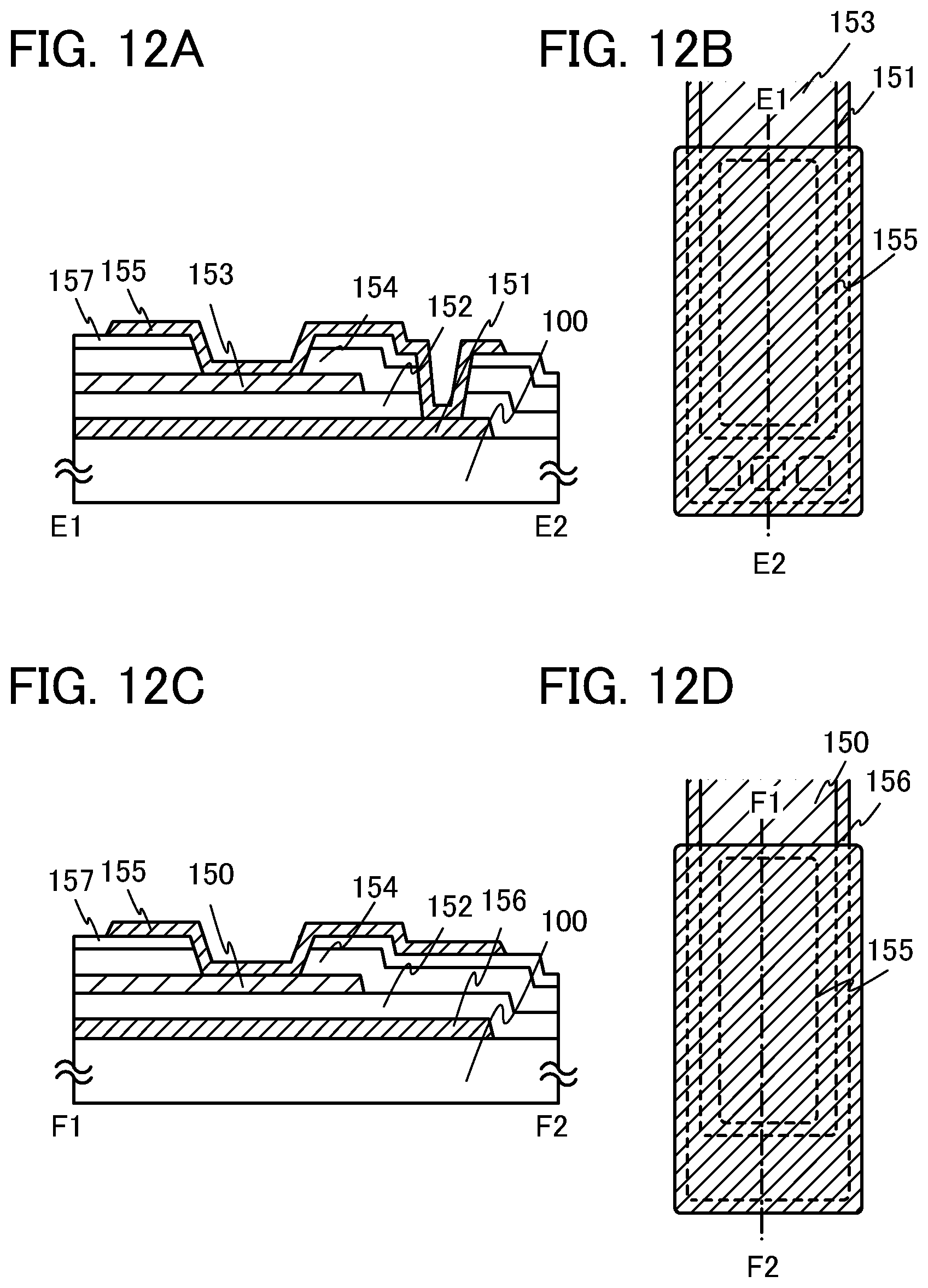
D00013

D00014

D00015

D00016
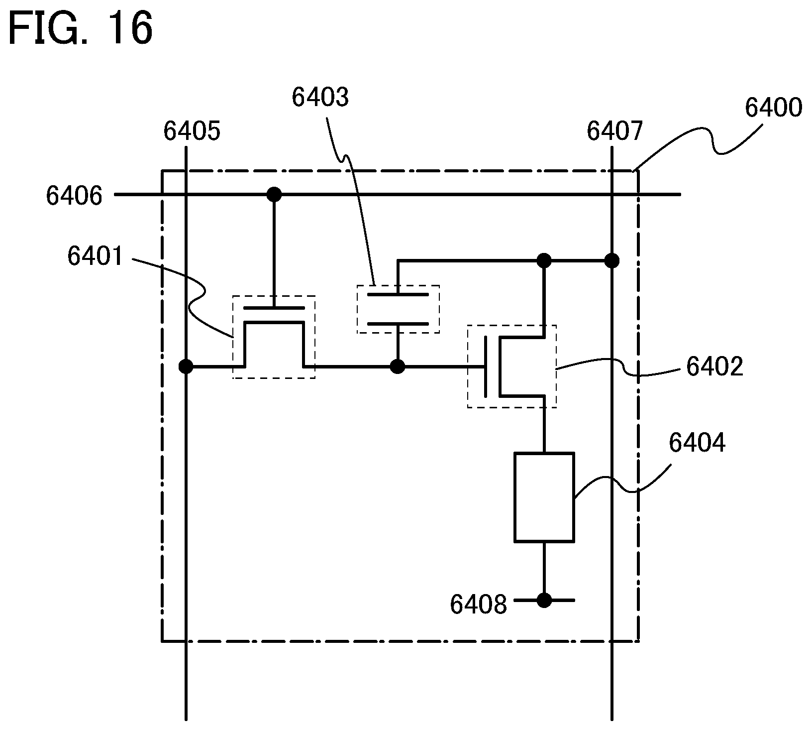
D00017

D00018

D00019

D00020

XML
uspto.report is an independent third-party trademark research tool that is not affiliated, endorsed, or sponsored by the United States Patent and Trademark Office (USPTO) or any other governmental organization. The information provided by uspto.report is based on publicly available data at the time of writing and is intended for informational purposes only.
While we strive to provide accurate and up-to-date information, we do not guarantee the accuracy, completeness, reliability, or suitability of the information displayed on this site. The use of this site is at your own risk. Any reliance you place on such information is therefore strictly at your own risk.
All official trademark data, including owner information, should be verified by visiting the official USPTO website at www.uspto.gov. This site is not intended to replace professional legal advice and should not be used as a substitute for consulting with a legal professional who is knowledgeable about trademark law.