Display Device and Driving Method Thereof
Yamazaki; Shunpei ; et al.
U.S. patent application number 16/657289 was filed with the patent office on 2020-03-05 for display device and driving method thereof. This patent application is currently assigned to Semiconductor Energy Laboratory Co., Ltd.. The applicant listed for this patent is Semiconductor Energy Laboratory Co., Ltd.. Invention is credited to Daisuke Kubota, Shunpei Yamazaki.
| Application Number | 20200074940 16/657289 |
| Document ID | / |
| Family ID | 60659711 |
| Filed Date | 2020-03-05 |


View All Diagrams
| United States Patent Application | 20200074940 |
| Kind Code | A1 |
| Yamazaki; Shunpei ; et al. | March 5, 2020 |
Display Device and Driving Method Thereof
Abstract
Power consumption of a display device is reduced. Display quality of a display device is improved. A high-quality image can be displayed regardless of a usage environment. The display device includes a first display element, a second display element, and a control portion. The first display device reflects visible light. The second display element emits visible light. The control portion is configured to drive the first display element and the second display element at the same time such that a maximum value of luminance of light emitted from the second display element is greater than or equal to 1% and less than or equal to 50% of maximum luminance on the assumption that maximum luminance of light which is emitted from the second display element is 100%.
| Inventors: | Yamazaki; Shunpei; (Tokyo, JP) ; Kubota; Daisuke; (Atsugi, JP) | ||||||||||
| Applicant: |
|
||||||||||
|---|---|---|---|---|---|---|---|---|---|---|---|
| Assignee: | Semiconductor Energy Laboratory
Co., Ltd. Kanagawa-ken JP |
||||||||||
| Family ID: | 60659711 | ||||||||||
| Appl. No.: | 16/657289 | ||||||||||
| Filed: | October 18, 2019 |
Related U.S. Patent Documents
| Application Number | Filing Date | Patent Number | ||
|---|---|---|---|---|
| 15623736 | Jun 15, 2017 | 10453401 | ||
| 16657289 | ||||
| Current U.S. Class: | 1/1 |
| Current CPC Class: | G09G 5/10 20130101; G09G 2360/144 20130101; G09G 2300/023 20130101; G09G 3/20 20130101; G09G 2330/021 20130101; G09G 2320/0626 20130101; G02F 2201/44 20130101; G09G 2340/0407 20130101; G02F 1/133555 20130101; G09G 3/3648 20130101; G09G 2300/046 20130101; G09G 2300/0456 20130101; G09G 3/34 20130101 |
| International Class: | G09G 3/34 20060101 G09G003/34; G09G 5/10 20060101 G09G005/10; G09G 3/20 20060101 G09G003/20 |
Foreign Application Data
| Date | Code | Application Number |
|---|---|---|
| Jun 17, 2016 | JP | 2016-121002 |
Claims
1. A method for driving a display device, the display device comprising: a first display element configured to reflect visible light; and a second display element configured to emit visible light, wherein when the first display element and the second display element are driven concurrently to display an image, a maximum value of luminance of light emitted from the second display element is greater than or equal to 5% and less than or equal to 50% of a maximum luminance of the second display element.
Description
[0001] This application is a continuation of copending U.S. application Ser. No. 15/623,736, filed on Jun. 15, 2017 which is incorporated herein by reference.
TECHNICAL FIELD
[0002] One embodiment of the present invention relates to a display device. One embodiment of the present invention relates to a method for driving the display device.
[0003] Note that one embodiment of the present invention is not limited to the above technical field. Examples of the technical field of one embodiment of the present invention disclosed in this specification and the like include a semiconductor device, a display device, a light-emitting device, a power storage device, a memory device, an electronic device, a lighting device, an input device, an input/output device, a driving method thereof, and a manufacturing method thereof.
[0004] In this specification and the like, a semiconductor device generally means a device that can function by utilizing semiconductor characteristics. A transistor, a semiconductor circuit, an arithmetic device, a memory device, and the like are each an embodiment of the semiconductor device. In addition, an imaging device, an electro-optical device, a power generation device (e.g., a thin film solar cell and an organic thin film solar cell), and an electronic device each may include a semiconductor device.
BACKGROUND ART
[0005] As one of display devices, there is a liquid crystal display device provided with a liquid crystal element. For example, an active matrix liquid crystal display device, in which pixel electrodes are arranged in a matrix and transistors are used as switching elements connected to respective pixel electrodes, has attracted attention.
[0006] For example, an active matrix liquid crystal display device including transistors, in which a metal oxide is used for a channel formation region, as switching elements connected to respective pixel electrodes is already known (Patent Documents 1 and 2).
[0007] It is known that an active matrix liquid crystal display device is classified into two major types: transmissive type and reflective type.
[0008] In a transmissive liquid crystal display device, a backlight such as a cold cathode fluorescent lamp or a light-emitting diode (LED) is used, and optical modulation action of liquid crystal is utilized to select one of the two states: a state where light from the backlight passes through liquid crystal to be output to the outside of the liquid crystal display device and a state where light is not output to the outside of the liquid crystal display device, whereby a bright or dark image is displayed. Furthermore, those images are combined to display an image.
[0009] In a reflective liquid crystal display device, a state in which external light, in other words, incident light is reflected at a pixel electrode and output to the outside of the device or a state in which incident light is not output to the outside of the device is selected using optical modulation action of a liquid crystal, whereby bright and dark images are displayed. Furthermore, those displays are combined to display an image. Compared with the transmissive liquid crystal display device, the reflective liquid crystal display device has the advantage of low power consumption since the backlight is not used.
REFERENCE
Patent Documents
[0010] [Patent Document 1] Japanese Published Patent Application No. 2007-123861
[0011] [Patent Document 2] Japanese Published Patent Application No. 2007-096055
DISCLOSURE OF INVENTION
[0012] Electronic devices including display devices are required to reduce their power consumption. In particular, since the energy consumption of display devices accounts for a significant proportion in devices in devices using batteries as power sources, such as mobile phones, smartphones, tablet terminals, smart watches, and notebook personal computers, low power consumption of display devices is required.
[0013] An object of one embodiment of the present invention is to reduce power consumption of a display device. Another object of one embodiment of the present invention is to improve display quality of a display device. Another object of one embodiment of the present invention is to display a high-quality image regardless of a usage environment.
[0014] Note that the descriptions of these objects do not disturb the existence of other objects. In one embodiment of the present invention, there is no need to achieve all the objects. Other objects can be derived from the description of the specification and the like.
[0015] One embodiment of the present invention is a method for driving a display device. The display device includes a first display element that reflects visible light and a second display element that emits visible light. When the first display element and the second display element are driven at the same time to display an image, a maximum value of luminance of light emitted from the second display element is greater than or equal to 5% and less than or equal to 50% of maximum luminance on the assumption that the maximum luminance of light which is emitted from the second display element is 100%.
[0016] Another embodiment of the present invention is a method for driving a display device. The display device includes a first display element that reflects visible light and a second display element that emits visible light. When the first display element is not driven and the second display element is driven to display an image, a maximum value of luminance of light emitted from the second display element is greater than or equal to 50% and less than or equal to 100% of maximum luminance on the assumption that the maximum luminance of light which is emitted from the second display element is 100%.
[0017] Another embodiment of the present invention is a display device including a first display element, a second display element, and a control portion. The first display element reflects visible light. The second display element emits visible light. The control portion is configured to drive the first display element and the second display element at the same time such that a maximum value of luminance of light emitted from the second display element is greater than or equal to 5% and less than or equal to 50% of maximum luminance on the assumption that the maximum luminance of light which is emitted from the second display element is 100%.
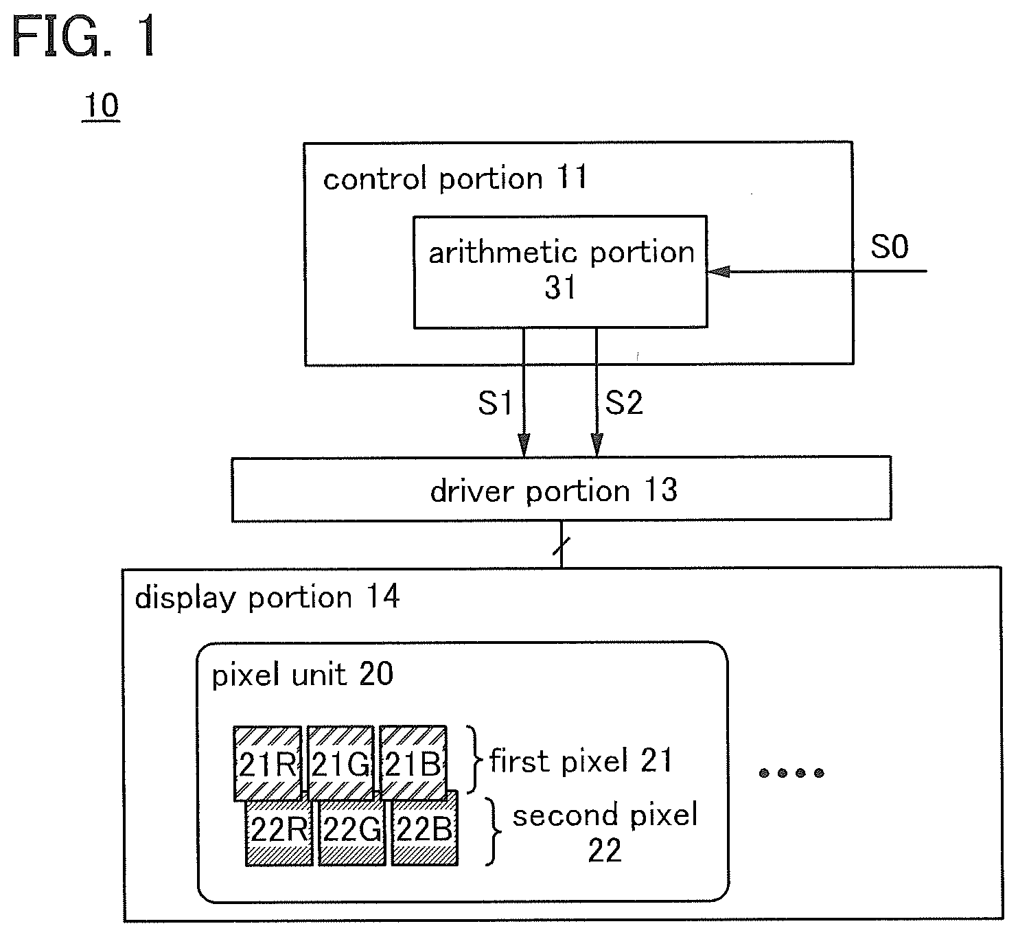
[0018] Another embodiment of the present invention is a display device including a first display element, a second display element, and a control portion. The first display element reflects visible light. The second display element emits visible light. The control portion is configured to not drive the first display element and to drive the second display element such that a maximum value of luminance of light emitted from the second display element is greater than or equal to 50% and less than or equal to 100% of maximum luminance on the assumption that the maximum luminance of light which is emitted from the second display element is 100%.
[0019] In the above, the second display element preferably includes an island-shaped first light-emitting layer that emits light of a predetermined color. At that time, a plurality of second display elements is arranged at a resolution of higher than or equal to 50 ppi and lower than 300 ppi.
[0020] In the above, it is preferable that the display device further include a coloring layer that is provided to overlap with the second display element. The second display element preferably includes a second light-emitting layer that emits white light. At that time, a plurality of second display elements is preferably arranged at a resolution of higher than or equal to 300 ppi and lower than or equal to 3000 ppi, preferably higher than or equal to 500 ppi and lower than or equal to 2500 ppi.
[0021] According to one embodiment of the present invention, power consumption of a display device can be reduced. Alternatively, display quality of a display device can be improved. Alternatively, a high-quality image can be displayed regardless of a usage environment.
[0022] Note that one embodiment of the present invention does not necessarily achieve all the effects listed above. Other effects will be apparent from and can be derived from the description of the specification, the drawings, the claims, and the like.
BRIEF DESCRIPTION OF THE DRAWINGS
[0023] FIG. 1 is a block diagram of a display device of one embodiment.
[0024] FIGS. 2A to 2C illustrate pixel units of one embodiment.
[0025] FIGS. 3A, 3B1 and 3B2 illustrate a display panel of one embodiment.
[0026] FIG. 4 is a circuit diagram of a display panel of one embodiment.
[0027] FIG. 5A is a circuit diagram of a display panel of one embodiment, and FIG. 5B is a structure example of a pixel of one embodiment.
[0028] FIG. 6 is a structure example of a display panel of one embodiment.
[0029] FIG. 7 is a structure example of a display panel of one embodiment.
[0030] FIG. 8 is a structure example of a display panel of one embodiment.
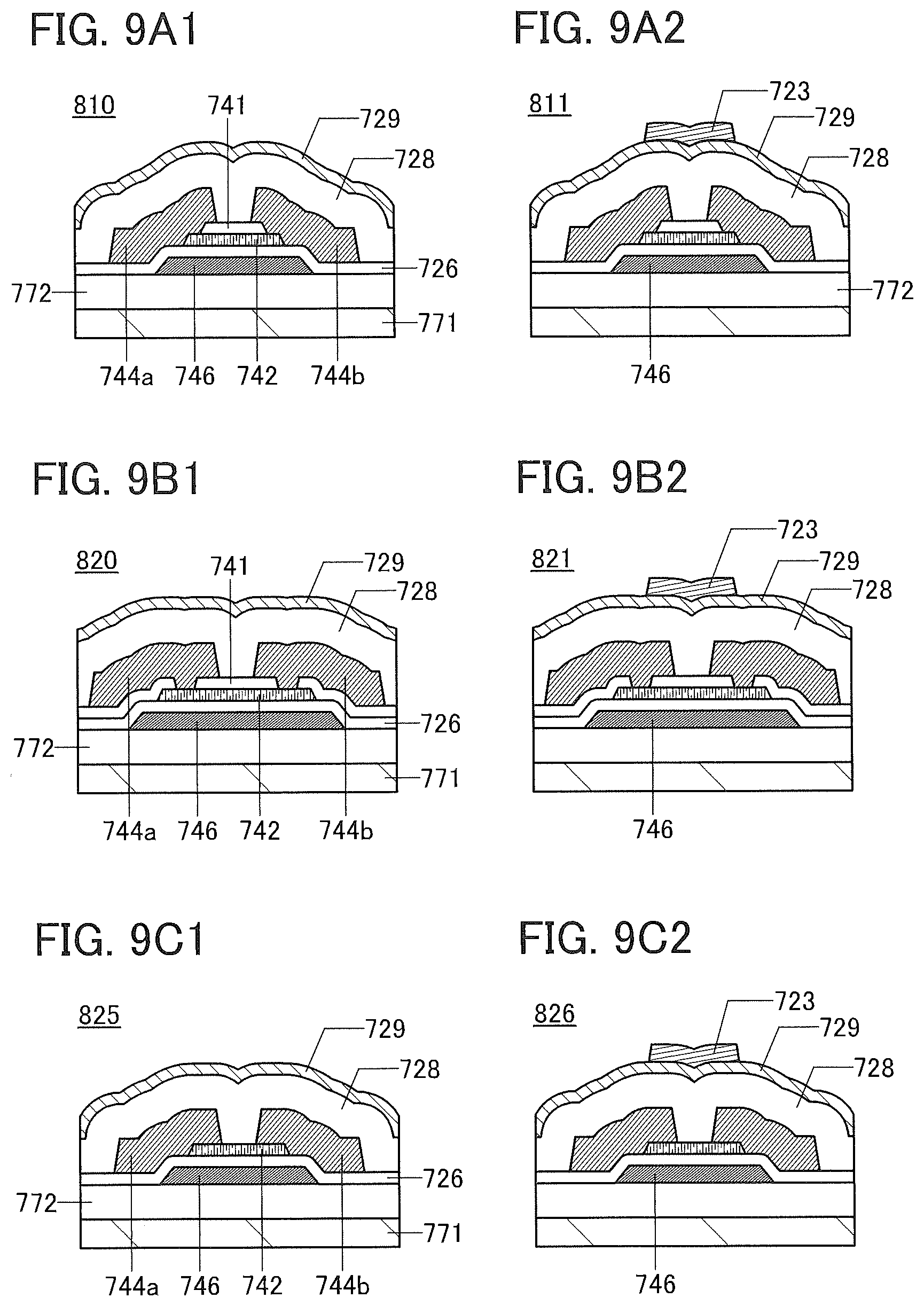
[0031] FIGS. 9A1, 9A2, 9B1, 9B2, 9C1, and 9C2 are structure examples of transistors of one embodiment.
[0032] FIGS. 10A1, 10A2, 10A3, 10B1, and 10B2 are structure examples of transistors of one embodiment.
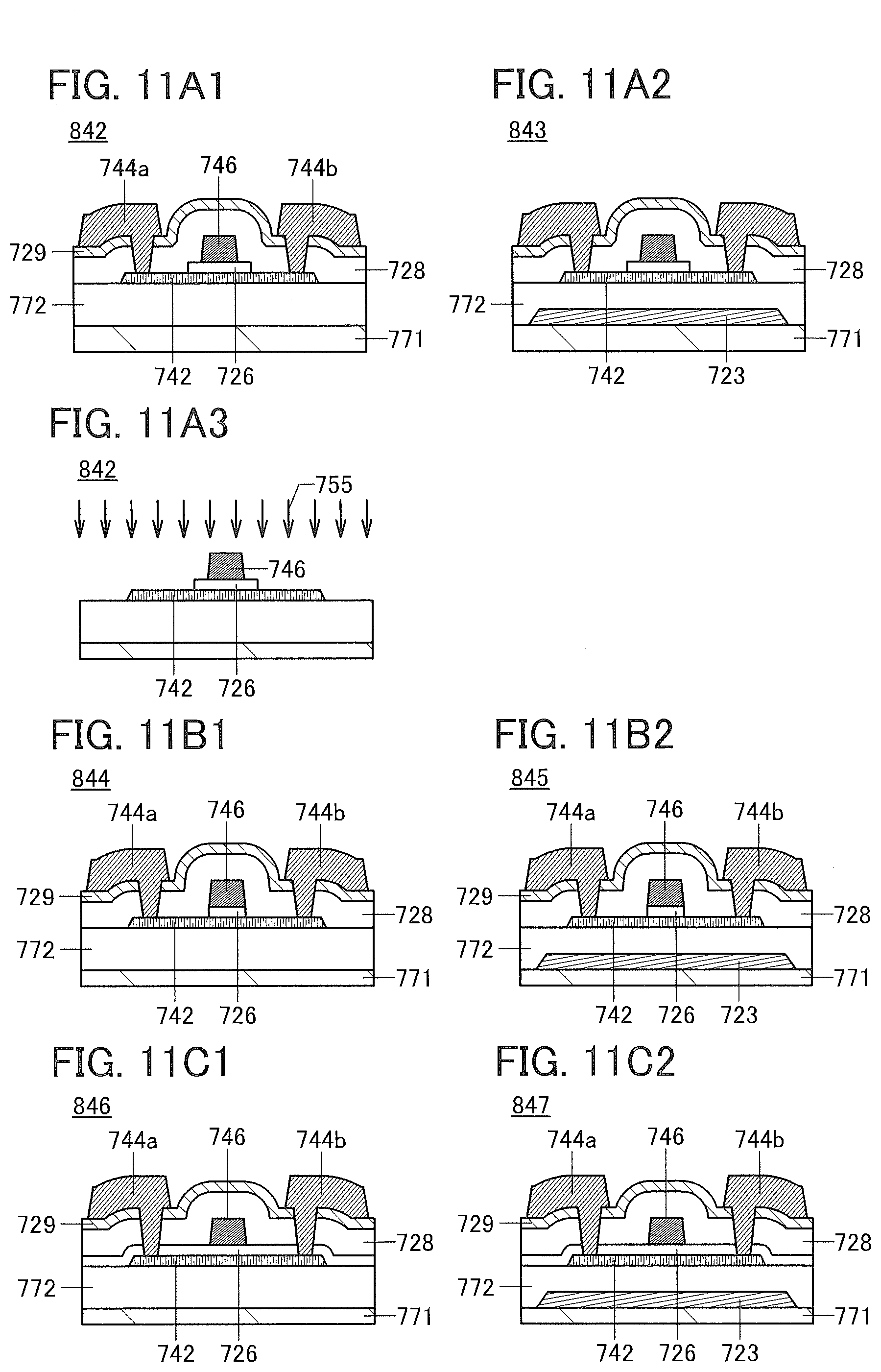
[0033] FIGS. 11A1, 11A2, 11A3, 11B1, 11B2, 11C1, and 11C2 are structure examples of transistors of one embodiment.
[0034] FIGS. 12A to 12F illustrate examples of electronic devices and a lighting device of one embodiment. FIGS. 13A to 13I illustrate examples of electronic devices of one embodiment.
[0035] FIGS. 14A to 14F illustrate examples of electronic devices of one embodiment.
BEST MODE FOR CARRYING OUT THE INVENTION
[0036] Embodiments are described in detail with reference to the drawings. Note that the present invention is not limited to the description below, and it is easily understood by those skilled in the art that various changes and modifications can be made without departing from the spirit and scope of the present invention. Thus, the present invention should not be construed as being limited to the description in the following embodiments.
[0037] Note that in structures of the present invention described below, the same portions or portions having similar functions are denoted by the same reference numerals in different drawings, and a description thereof is not repeated. Further, the same hatching pattern is used for portions having similar functions, and the portions are not especially denoted by reference numerals in some cases.
[0038] Note that in each drawing described in this specification, the size, the layer thickness, or the region of each component is exaggerated for clarity in some cases. Therefore, embodiments of the present invention are not limited to such a scale.
[0039] Note that in this specification and the like, ordinal numbers such as "first," "second," and the like are used in order to avoid confusion among components and do not limit the number.
[0040] A transistor is a kind of semiconductor elements and can achieve amplification of current and voltage, switching operation for controlling conduction and non-conduction, and the like. A transistor in this specification includes an insulated-gate field effect transistor (IGFET) and a thin film transistor (TFT).
Embodiment 1
[0041] In this embodiment, a display device of one embodiment of the present invention and a driving method thereof are described.
[0042] In the display device of one embodiment of the present invention, a first display element that reflects visible light and a second display element that emits visible light are mixed.
[0043] The display device has a function of displaying an image utilizing one or both of first light reflected by the first display element and second light emitted from the second display element. Alternatively, the display device has a function of expressing gray scales by individually controlling the amount of first light reflected by the first display element and the amount of second light emitted from the second display element.
[0044] It is preferable that the display device have a structure including a first pixel expressing gray scales by controlling the amount of light reflected from the first display element and a second pixel expressing gray scales by controlling the amount of light emitted from the second display element. For example, the first pixels are arranged in a matrix and the second pixels are arranged in a matrix to form a display portion.
[0045] The number of the first pixels is preferably the same as that of the second pixels, and the first pixels and the second pixels are preferably arranged in a display region with the same pitch. Here, the first pixel and the second pixel adjacent to each other can be collectively referred to as a pixel unit.
[0046] Furthermore, the first pixels and the second pixels are preferably mixed in the display region of the display device. Accordingly, as described later, an image displayed by a plurality of first pixels, an image displayed by a plurality of second pixels, and an image displayed by both the plurality of first pixels and the plurality of second pixels can be displayed in the same display region.
[0047] As the first display element included in the first pixel, an element that performs display by reflecting external light can be used. Such an element does not include a light source and thus power consumption in display can be significantly reduced.
[0048] As the first display element, a reflective liquid crystal element can be typically used. As the first display element, other than a Micro Electro Mechanical Systems (MEMS) shutter element and an optical interference type MEMS element, an element using a microcapsule method, an electrophoretic method, an electrowetting method, an Electronic Liquid Powder (registered trademark) method, or the like can be used.
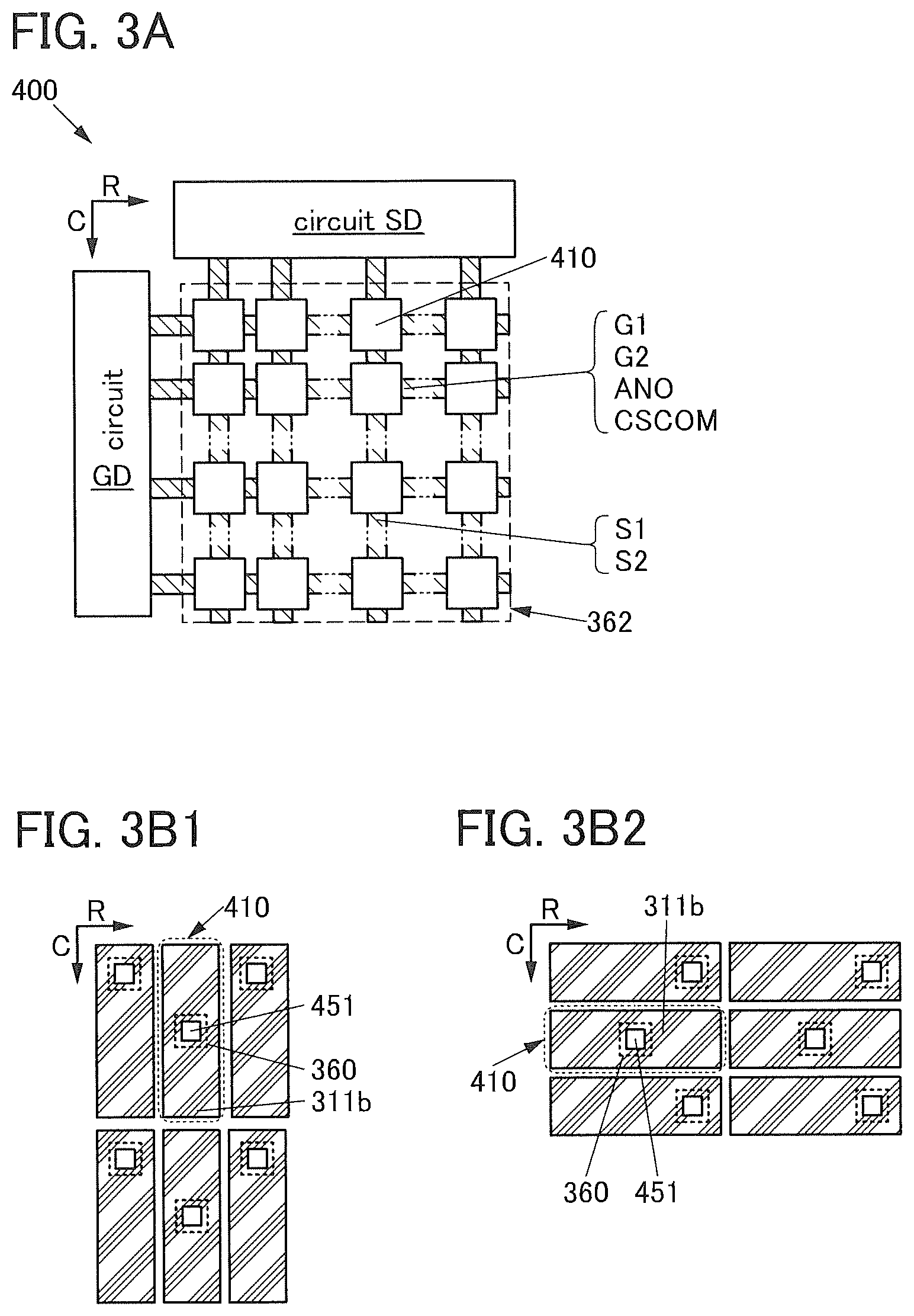
[0049] As the second display element included in the second pixel, an element including a light source and performing display using light from the light source can be used. Specifically, it is preferable to use an electroluminescence element in which light can be extracted from a light-emitting substance by application of an electric field. Since the luminance and the chromaticity of light emitted from such a pixel are not affected by external light, an image with high color reproducibility (a wide color gamut) and a high contrast, i.e., a vivid image can be displayed.
[0050] As the second display element, a self-luminous light-emitting element such as an organic light-emitting diode (OLED), a light-emitting diode (LED), and a quantum-dot light-emitting diode (QLED) can be used. Alternatively, a combination of a backlight that is a light source and a transmissive liquid crystal element controlling the amount of light transmitted from the backlight may be used as the display element included in the second pixel.
[0051] The first pixel can include, for example, subpixels emitting light of white (W), or subpixels emitting light of three colors of red (R), green (G), and blue (B), respectively. Similarly, the second pixel can include, for example, subpixels emitting light of white (W), or subpixels emitting light of three colors of red (R), green (G), and blue (B), respectively. Note that the first pixel and the second pixel may each include subpixels of four colors or more. As the number of subpixels is increased, power consumption can be reduced and color reproducibility can be improved.
[0052] In one embodiment of the present invention, a first mode in which an image is displayed by the first pixels, a second mode in which an image is displayed by the second pixels, and a third mode in which an image is displayed by the first pixels and the second pixels can be switched.
[0053] The first mode is a mode in which an image is displayed utilizing light reflected from the first display element. In the first mode, a light source is not necessary and thus the first mode is a driving mode with extremely low power consumption. The first mode is effective in the case where, for example, external light has a sufficiently high illuminance and is white light or light near white light. The first mode is a display mode appropriate for displaying text data, such as that of a book or that of a document. Use of reflected light enables eye-friendly display, thereby mitigating eye fatigue.
[0054] The second mode is a mode in which an image is displayed utilizing light emitted from the second display element. Thus, an extremely vivid image (high contrast and high color reproducibility) can be displayed regardless of the illuminance and chromaticity of external light. For example, the second mode is effective in the case where the illuminance of external light is extremely low, such as during the night or in a dark room. When a bright image is displayed under weak external light, a user may feel that the image is too bright. To prevent this, an image with reduced luminance is preferably displayed in the second mode. Thus, not only a reduction in the luminance but also low power consumption can be achieved. The second mode is a mode suitable for obtaining a vivid image and a smooth moving image.
[0055] The third mode is a mode in which display is performed using both light reflected from the first display element and light emitted from the second display element. Specifically, the display device is driven so that light emitted from the first pixel and light emitted from the second pixel adjacent to the first pixel are mixed to express one color. Accordingly, a more vivid image than that in the first mode can be displayed and power consumption can be made lower than that in the second mode. For example, the third mode is effective when the illuminance of external light is relatively low such as under indoor illumination or in the morning or evening, or when the external light does not represent a white chromaticity. Furthermore, the use of light obtained by mixing reflected light and emitted light makes it possible to display an image that gives a viewer the impression of seeing a picture.
[0056] Here, in the third mode in which an image is displayed using both light reflected from the first display element and light emitted from the second display element, luminance of the second display element is preferably reduced. For example, on the assumption that a maximum value of luminance (also referred to as maximum luminance) of light which is emitted from the second display element is 100%, a maximum value of luminance of light emitted from the second display element in the third mode is preferably greater than or equal to 5% and less than or equal to 50%, preferably greater than or equal to 1% and less than or equal to 60% of the maximum luminance. Accordingly, display with low power consumption can be achieved, a picture-like image can be displayed, and eye-friendly display can be performed.
[0057] Furthermore, in the second mode in which only a display element that emits visible light is used, luminance of the display element that emits visible light is preferably increased. For example, a maximum value of luminance of light emitted from the second display element in the second mode can be 100%, or greater than or equal to 50% and less than or equal to 100%, preferably greater than or equal to 60% and less than or equal to 100% of the maximum luminance. Accordingly, a vivid image can be displayed even in a place with bright external light.
[0058] Here, the maximum value of luminance of light emitted from the second display element can be expressed by a dynamic range of the second display element. That is, the dynamic range of the second display element in the third mode can be set narrower than that in the second mode. For example, the dynamic range of the second display element in the third mode can be set at greater than or equal to 5% and less than or equal to 50%, preferably greater than or equal to 1% and less than or equal to 60% of the dynamic range of the second display element in the second mode.
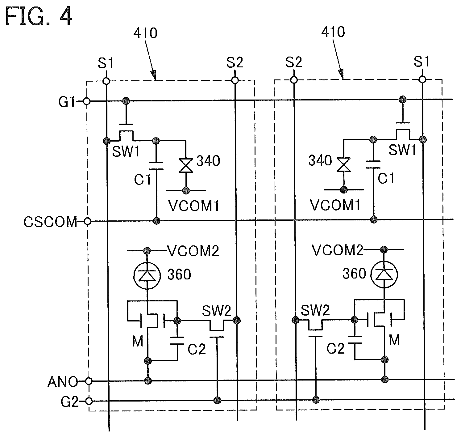
[0059] More specifically, the display device can include a display panel including the first and second pixels, and a control portion. The control portion generates and outputs a first gray level and a second gray level to the first pixel and the second pixel, respectively, on the basis of image data input from the outside. Here, the image data is data including a gray level corresponding to each pixel unit, and an image signal such as a video signal is given as an example.
[0060] Note that the control portion may have a function of selecting the above-described display modes on the basis of external light illuminance and the like.
[0061] A more specific example of one embodiment of the present invention is described below with reference to drawings.
Structure Example of Display Device
[0062] FIG. 1 is a block diagram of a display device 10 of one embodiment of the present invention. The display device 10 includes a control portion 11, a driver portion 13, and a display portion 14. The display device 10 may have a photometric portion which measures external light illuminance and the like.
[0063] The control portion 11 includes an arithmetic portion 31.
[0064] The display portion 14 includes a plurality of pixel units 20 arranged in a matrix. The pixel unit 20 includes a first pixel 21 and a second pixel 22.
[0065] FIG. 1 shows an example where the first pixel 21 and the second pixel 22 each include display elements corresponding to three colors of red (R), green (G), and blue (B).
[0066] The first pixel 21 includes a display element 21R corresponding to red (R), a display element 21G corresponding to green (G), and a display element 21B corresponding to blue (B). The display elements 21R, 21G, and 21B each utilize reflection of external light.
[0067] The second pixel 22 includes a display element 22R corresponding to red (R), a display element 22G corresponding to green (G), and a display element 22B corresponding to blue (B). The display elements 22R, 22G, and 22B each utilize light of a light source.
[0068] The driver portion 13 includes a circuit for driving the plurality of pixel units 20 in the display portion 14. Specifically, the driver portion 13 includes a circuit that supplies a signal including a gray level, a scan signal, a power supply potential, and the like to the first pixel 21 and the second pixel 22 included in the pixel unit 20. The driver portion 13 includes a signal line driver circuit and a scan line driver circuit, for example.
[0069] A image signal S0 including image data is input to the control portion 11 from the outside. The control portion 11 generates two signals (a signal S1 and a signal S2) including gray levels supplied to each pixel unit 20 in the display portion 14, and outputs the signals to the driver portion 13. The control portion 11 generates a timing signal such as a clock signal or a start pulse signal in addition to the signals Si and S2 and outputs the signals to the driver portion 13.
[0070] The signal S1 includes a gray level supplied to the first pixel 21 in the pixel unit 20. Here, the signal S1 includes data of three gray levels supplied to the respective display elements 21R, 21G, and 21B in one pixel unit 20.
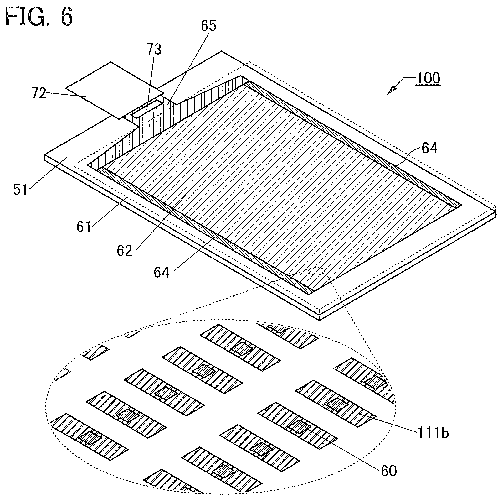
[0071] The signal S2 includes gray levels supplied to the second pixel 22 in the pixel unit 20. Here, the signal S2 includes data of three gray levels supplied to the respective display elements 22R, 22G, and 22B in one pixel unit 20.
[0072] The signals S1 and S2 each may be a serial signal transmitted through one signal line or a parallel signal transmitted through a plurality of signal lines.
[0073] The control portion 11 is configured to select one of the first mode, the second mode, and the third mode described below, generate the signals S1 and S2 based on the respective modes, and output the signals to the driver portion 13.
[0074] For example, in the third mode in which both a display element that reflects external light and a display element that emits light are driven to display an image, the control portion 11 is configured to drive the display element that reflects external light and the display element that emits light at the same time such that a maximum value of luminance of light emitted from the display element that emits light is greater than or equal to 5% and less than or equal to 50%, preferably greater than or equal to 1% and less than or equal to 60% of maximum luminance on the assumption that the maximum luminance of light which is emitted from the display element that emits light is 100%.
[0075] Furthermore, for example, in the second mode in which the display element that emits light is driven to display an image, the control portion 11 is configured to not drive the display element that reflects external light and to drive the display element that emits light such that the maximum value of luminance of light emitted from the display element that emits light is 100%, or greater than or equal to 50% and less than or equal to 100%, preferably greater than or equal to 60% and less than or equal to 100% of maximum luminance on the assumption that the maximum luminance of light which is emitted from the display element that emits light is 100%.
[0076] Here, a microprocessor such as a graphics processing unit (GPU) can be used as the arithmetic portion 31, for example. Furthermore, such a microprocessor may be obtained with a programmable logic device (PLD) such as a field programmable gate array (FPGA) or a field programmable analog array (FPAA).
[0077] Here, the image signal S0 may be generated by a central processing unit (CPU) or the like provided separately from the display device 10 and supplied to the control portion 11. Alternatively, the arithmetic portion 31 may serve as a CPU and have a function of generating the image signal S0.
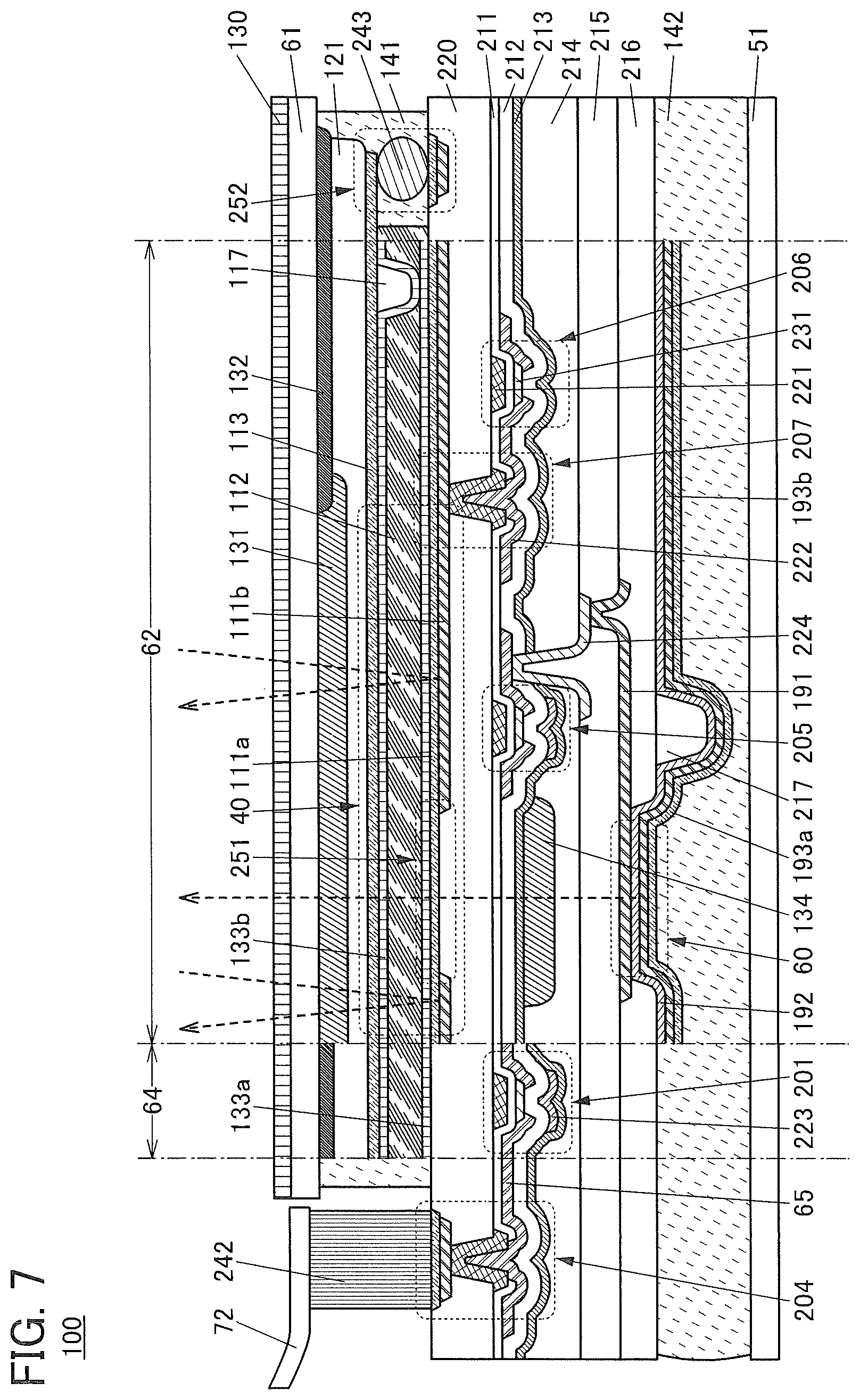
[0078] The image signal S0 input from the outside may be a signal that has already been subjected to gamma correction. The arithmetic portion 31 may have a function of performing the correction. The arithmetic portion 31 may generate the signals S1 and S2 based on a signal resulting from correction being performed on the image signal S0 or may correct each of generated signals S1 and S2.
[0079] The arithmetic portion 31 interprets and executes instructions from programs to process various kinds of data and control programs. The programs executed by the processor may be stored in a memory region included in the processor or a memory device which is additionally provided.
[0080] The arithmetic portion 31 may include a main memory. The main memory can include a volatile memory, such as a random access memory (RAM), and a nonvolatile memory, such as a read only memory (ROM).
[0081] For example, a dynamic random access memory (DRAM) is used for the RAM. A memory space as a workspace for the arithmetic portion 31 is virtually allocated for the RAM and used in the arithmetic portion 31. An operating system, an application program, a program module, program data, and the like stored in a memory device provided outside are loaded into the RAM and executed. The data, program, and program module which are loaded into the RAM are directly accessed and operated by the arithmetic portion 31.
[0082] The control portion 11 may be mounted on a circuit board such as a printed circuit, and the driver portion 13 may be provided over a substrate over which the display portion 14 is formed. Here, the circuit board and the driver portion 13 are connected to each other via a flexible printed circuit (FPC) or the like. Furthermore, the driver portion 13 may be formed over a substrate over which the display portion 14 is formed through the same step as transistors and the like included in the display portion 14, and part or all of the driver portion 13 may be mounted on the substrate as an integrated circuit (IC). Alternatively, the control portion 11 and the driver portion 13 may be mounted on the substrate as one or more ICs. Alternatively, the control portion 11 and the driver portion 13 may be formed over a substrate over which the display portion 14 is formed through the same step as transistors included in the display portion 14.
[0083] That is the description of the structure examples of the display device.
Structure Example of Pixel Unit
[0084] Next, the pixel unit 20 is explained with reference to FIGS. 2A to 2C. FIGS. 2A to 2C are schematic views illustrating structure examples of the pixel unit 20.
[0085] The first pixel 21 includes the display elements 21R, 21G, and 21B. The display element 21R reflects external light and emits red light R1, to the display surface side, with luminance in accordance with a gray level corresponding to red included in the first gray level input to the first pixel 21. Similarly, the display element 21G and the display element 21B emit green light G1 and blue light B1, respectively, to the display surface side.
[0086] The second pixel 22 includes the display elements 22R, 22G, and 22B. The display element 22R includes a light source and emits red light R2, to the display surface side, with luminance in accordance with a gray level corresponding to red included in the second gray level input to the second pixel 22. Similarly, the display element 22G and the display element 22B emit green light G2 and blue light B2, respectively, to the display surface side.
Third Mode
[0087] FIG. 2A illustrates an example of an operation mode in which both the display elements 21R, 21G, and 21B that reflect external light and the display elements 22R, 22G, and 22B that emit light are driven to display an image. As illustrated in FIG. 2A, the pixel unit 20 can emit light 25 of a predetermined color to the display surface side by mixing light of six colors, the light R1, the light G1, the light B1, the light R2, the light G2, and the light B2.
[0088] At this time, luminance of each of the display elements 22R, 22G, and 22B is preferably lowered. For example, on the assumption that the maximum value of luminance (also referred to as maximum luminance) of light which is emitted from each of the display elements 22R, 22G, and 22B is 100%, the maximum value of luminance of light emitted from each of the display elements 22R, 22G, and 22B in the third mode is greater than or equal to 5% and less than or equal to 50%, preferably greater than or equal to 1% and less than or equal to 60% of the maximum luminance. Accordingly, display with low power consumption can be achieved, a picture-like image can be displayed, and eye-friendly display can be achieved.
First Mode
[0089] FIG. 2B illustrates an example of an operation mode in which the display elements 21R, 21G, and 21B that reflect external light are driven to display an image. As illustrated in FIG. 2B, in the case where illuminance of external light is sufficiently high, for example, the pixel unit 20 can emit the light 25 of a predetermined color to the display surface side by not driving the second pixel 22 and mixing only light (the light R1, the light G1, and the light B1) from the first pixel 21. Thus, driving with extremely low power consumption can be performed.
Second Mode
[0090] FIG. 2C illustrates an example of an operation mode in which the display elements 22R, 22G, and 22B are driven to display an image. As illustrated in FIG. 2C, in the case where illuminance of external light is extremely low, for example, the pixel unit 20 can emit the light 25 of a predetermined color to the display surface side by not driving the first pixel 21 and mixing only light (the light R2, the light G2, and the light B2) from the second pixel 22. Accordingly, a clear image can be displayed. Furthermore, luminance is lowered when illuminance of external light is low, which can prevent a user from feeling glare and reduce power consumption.
[0091] At this time, the luminance of the display elements that emit visible light in the second mode is preferably higher than that in the third mode. For example, the maximum value of luminance of light emitted from each of the display elements 22R, 22G, and 22B in the second mode can be 100%, or greater than or equal to 50% or less than or equal to 100%, preferably greater than or equal to 60% or less than or equal to 100% of the maximum luminance. Accordingly, a vivid image can be displayed even in a place with bright external light.
[0092] Here, the maximum value of luminance of light emitted from each of the display elements 22R, 22G, and 22B can be replaced with a dynamic range thereof. That is, the dynamic range of each of the display elements 22R, 22G, and 22B in the third mode can be set narrower than that in the second mode. For example, the dynamic range of each of the display elements 22R, 22G, and 22B in the third mode is set to be greater than or equal to 5% and less than or equal to 50%, preferably greater than or equal to 1% and less than or equal to 60% of the dynamic range of the second mode.
[0093] The above is the description of the structure example of the pixel unit 20.
[0094] At least part of this embodiment can be implemented in combination with any of the other embodiments described in this specification as appropriate.
Embodiment 2
[0095] An example of a display panel that can be used for the display portion or the like of the display device of one embodiment of the present invention is described below. The display panel described below as an example includes both a reflective liquid crystal element and a light-emitting element and can display an image both in a transmissive mode and in a reflective mode.
Structure Example
[0096] FIG. 3A is a block diagram illustrating an example of the structure of a display device 400. The display device 400 includes a plurality of pixels 410 that are arranged in a matrix in a display portion 362. The display device 400 also includes a circuit GD and a circuit SD. In addition, the display device 400 includes a plurality of wirings G1, a plurality of wirings G2, a plurality of wirings ANO, and a plurality of wirings CSCOM, which are electrically connected to the circuit GD and the plurality of pixels 410 arranged in a direction R. Moreover, the display device 400 includes the plurality of pixels 410 arranged in a direction C, and a plurality of wirings S1 and a plurality of wirings S2 that are electrically connected to the circuit SD.
[0097] Although the display device includes one circuit GD and one circuit SD here for simplification, the circuit GD and the circuit SD for driving a liquid crystal element and the circuit GD and the circuit SD for driving a light-emitting element may be separately provided.
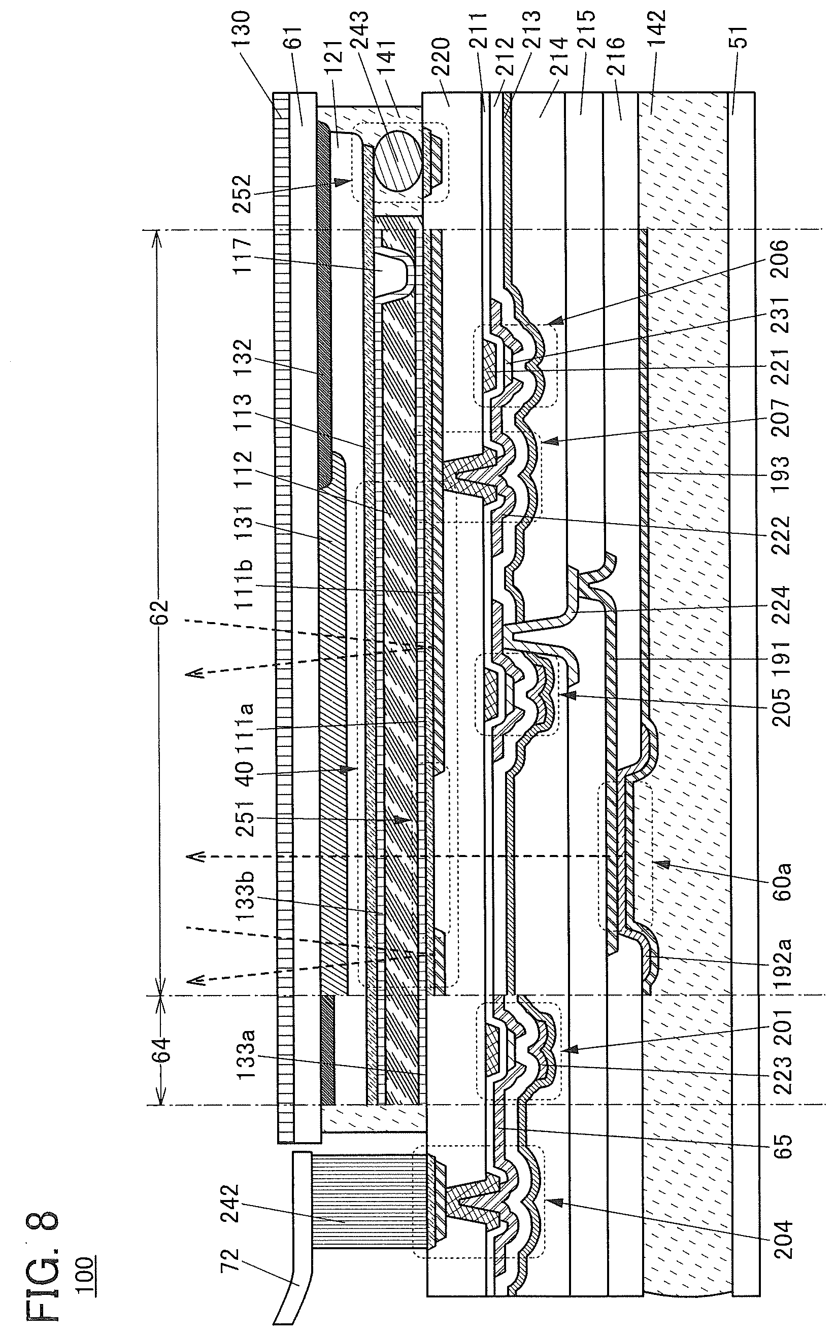
[0098] The pixel 410 includes a reflective liquid crystal element and a light-emitting element. In the pixel 410, the liquid crystal element and the light emitting element partly overlap with each other.
[0099] FIG. 3B1 illustrates a structure example of an electrode 311b included in the pixel 410. The electrode 311b serves as a reflective electrode of the liquid crystal element in the pixel 410. The electrode 311b has an opening 451.
[0100] In FIG. 3B1, the light-emitting element 360 in a region overlapping with the electrode 311b is denoted by a dashed line. The light-emitting element 360 overlaps with the opening 451 included in the electrode 311b. Thus, light from the light-emitting element 360 is emitted to a display surface side through the opening 451.
[0101] In FIG. 3B1, the pixels 410 adjacent in the direction R correspond to different colors. As illustrated in FIG. 3B1, the openings 451 are preferably provided in different positions in the electrodes 311b so as not to be aligned in the two pixels adjacent to each other in the direction R. This allows the two light-emitting elements 360 to be apart from each other, thereby preventing light emitted from the light-emitting element 360 from entering a coloring layer in the adjacent pixel 410 (such a phenomenon is also referred to as crosstalk). Furthermore, since the two adjacent light-emitting elements 360 can be arranged apart from each other, a high-resolution display device is achieved even when EL layers of the light-emitting elements 360 are separately formed with a shadow mask or the like.
[0102] Alternatively, arrangement illustrated in FIG. 3B2 may be employed.
[0103] If the ratio of the total area of the opening 451 to the total area except for the opening is too large, display performed using the liquid crystal element is dark. If the ratio of the total area of the opening 451 to the total area except for the opening is too small, display performed using the light-emitting element 360 is dark.
[0104] If the area of the opening 451 in the electrode 311b serving as a reflective electrode is too small, light emitted from the light-emitting element 360 is not efficiently extracted.
[0105] The opening 451 may have a polygonal shape, a quadrangular shape, an elliptical shape, a circular shape, a cross-like shape, a stripe shape, a slit-like shape, or a checkered pattern, for example. The opening 451 may be provided close to the adjacent pixel. Preferably, the opening 451 is provided close to another pixel emitting light of the same color, in which case crosstalk can be suppressed.
Circuit Structure Example
[0106] FIG. 4 is a circuit diagram illustrating a structure example of the pixel 410. FIG. 4 shows two adjacent pixels 410.
[0107] The pixel 410 includes a switch SW1, a capacitor C1, a liquid crystal element 340, a switch SW2, a transistor M, a capacitor C2, the light-emitting element 360, and the like. The pixel 410 is electrically connected to the wiring G1, the wiring G2, the wiring ANO, the wiring CSCOM, the wiring S1, and the wiring S2. FIG. 4 illustrates a wiring VCOM1 electrically connected to the liquid crystal element 340 and a wiring VCOM2 electrically connected to the light-emitting element 360.
[0108] FIG. 4 illustrates an example in which a transistor is used as each of the switches SW1 and SW2.
[0109] A gate of the switch SW1 is connected to the wiring G1. One of a source and a drain of the switch SW1 is connected to the wiring S1, and the other of the source and the drain is connected to one electrode of the capacitor C1 and one electrode of the liquid crystal element 340. The other electrode of the capacitor C1 is connected to the wiring CSCOM. The other electrode of the liquid crystal element 340 is connected to the wiring VCOM1.
[0110] A gate of the switch SW2 is connected to the wiring G2. One of a source and a drain of the switch SW2 is connected to the wiring S2, and the other of the source and the drain is connected to one electrode of the capacitor C2 and a gate of the transistor M. The other electrode of the capacitor C2 is connected to one of a source and a drain of the transistor M and the wiring ANO. The other of the source and the drain of the transistor M is connected to one electrode of the light-emitting element 360. The other electrode of the light-emitting element 360 is connected to the wiring VCOM2.
[0111] FIG. 4 illustrates an example in which the transistor M includes two gates between which a semiconductor is provided and which are connected to each other. This structure can increase the amount of current flowing through the transistor M.
[0112] The wiring G1 can be supplied with a signal for changing the on/off state of the switch SW1. A predetermined potential can be supplied to the wiring VCOM1. The wiring S1 can be supplied with a signal for changing the orientation of liquid crystals of the liquid crystal element 340. A predetermined potential can be supplied to the wiring CSCOM.
[0113] The wiring G2 can be supplied with a signal for changing the on/off state of the switch SW2. The wiring VCOM2 and the wiring ANO can be supplied with potentials having a difference large enough to make the light-emitting element 360 emit light. The wiring S2 can be supplied with a signal for changing the conduction state of the transistor M.
[0114] In the case of performing display in the reflective mode, the pixel 410 shown in FIG. 4 can display an image by being driven with signals supplied to the wiring G1 and the wiring S1 and by utilizing optical modulation of the liquid crystal element 340. Furthermore, in the case of performing display in the transmissive mode, the pixel 410 shown in FIG. 4 can display an image by being driven with signals supplied to the wiring G2 and the wiring S2 and by making the light-emitting element 360 emit light. Furthermore, an image can be displayed while driving the pixel in both modes with the signals supplied to the wiring G1, the wiring G2, the wiring S1, and the wiring S2.
[0115] Although FIG. 4 illustrates an example in which one liquid crystal element 340 and one light-emitting element 360 are provided in one pixel 410, one embodiment of the present invention is not limited thereto. FIG. 5A illustrates an example in which one liquid crystal element 340 and four light-emitting elements 360 (light-emitting elements 360r, 360g, 360b, and 360w) are provided in one pixel 410. The pixel 410 in FIG. 5A is capable of full color display by one pixel, which is different from the pixel in FIG. 4.
[0116] In FIG. 5A, in addition to the example of FIG. 4, a wiring G3 and a wiring S3 are connected to the pixel 410.
[0117] In the example of FIG. 5A, light-emitting elements emitting red light (R), green light (G), blue light (B), and white light (W) can be used for the four light-emitting elements 360, for example. Furthermore, as the liquid crystal element 340, a reflective liquid crystal element emitting white light can be used. In the case of performing display in the reflective mode, white display with high reflectivity can be performed. In the case of performing display in the transmissive mode, images can be displayed with a higher color rendering property at low power consumption.
[0118] FIG. 5B illustrates a structure example of the pixel 410. The pixel 410 includes the light-emitting element 360w which overlaps with the opening of an electrode 311 and the light-emitting element 360r, 360g, and 360b which are provided in the periphery of the electrode 311. It is preferable that the light-emitting elements 360r, 360g, and 360b have almost the same light-emitting area.
Structure Example of Display Panel
[0119] FIG. 6 is a schematic perspective view illustrating a display panel 100 of one embodiment of the present invention. In the display panel 100, a substrate 51 and a substrate 61 are attached to each other. In FIG. 6, the substrate 61 is denoted by a dashed line.
[0120] The display panel 100 includes a display portion 62, a circuit 64, a wiring 65, and the like. The substrate 51 is provided with the circuit 64, the wiring 65, a conductive layer 111b which serves as a pixel electrode, and the like. In FIG. 6, an IC 73 and an FPC 72 are mounted on the substrate 51. Thus, the structure illustrated in FIG. 6 can be referred to as a display module including the display panel 100, the FPC 72, and the IC 73.
[0121] As the circuit 64, for example, a circuit functioning as a scan line driver circuit can be used.
[0122] The wiring 65 has a function of supplying a signal or electric power to the display portion 62 or the circuit 64. The signal or electric power is input to the wiring 65 from the outside through the FPC 72 or from the IC 73.
[0123] FIG. 6 shows an example in which the IC 73 is provided on the substrate 51 by a chip on glass (COG) method or the like. As the IC 73, an IC functioning as a scan line driver circuit, a signal line driver circuit, or the like can be used. Note that it is possible that the IC 73 is not provided when, for example, the display panel 100 includes circuits serving as a scan line driver circuit and a signal line driver circuit and when the circuits serving as a scan line driver circuit and a signal line driver circuit are provided outside and a signal for driving the display panel 100 is input through the FPC 72. Alternatively, the IC 73 may be mounted on the FPC 72 by a chip on film (COF) method or the like.
[0124] FIG. 6 also shows an enlarged view of part of the display portion 62. The conductive layers 111b included in a plurality of display elements are arranged in a matrix in the display portion 62. The conductive layer 111b has a function of reflecting visible light and serves as a reflective electrode of the liquid crystal element 40 described later.
[0125] As illustrated in FIG. 6, the conductive layer 111b has an opening. The light-emitting element 60 is provided on the substrate 51 side of the conductive layer 111b. Light is emitted from the light-emitting element 60 to the substrate 61 side through the opening in the conductive layer 111b.
Cross-Sectional Structure Example
[0126] FIG. 7 shows an example of cross sections of part of a region including the FPC 72, part of a region including the circuit 64, and part of a region including the display portion 62 of the display panel illustrated in FIG. 6.
[0127] The display panel includes an insulating layer 220 between the substrates 51 and 61. The display panel also includes the light-emitting element 60, a transistor 201, a transistor 205, a transistor 206, a coloring layer 134, and the like between the substrate 51 and the insulating layer 220. Furthermore, the display panel includes the liquid crystal element 40, the coloring layer 131 and the like between the insulating layer 220 and the substrate 61. The substrate 61 and the insulating layer 220 are bonded with an adhesive layer 141. The substrate 51 and the insulating layer 220 are bonded with an adhesive layer 142.
[0128] The transistor 206 is electrically connected to the liquid crystal element 40 and the transistor 205 is electrically connected to the light-emitting element 60. Since the transistors 205 and 206 are formed on a surface of the insulating layer 220 which is on the substrate 51 side, the transistors 205 and 206 can be formed through the same process.
[0129] The coloring layer 131, a light-blocking layer 132, an insulating layer 121, and a conductive layer 113 serving as a common electrode of the liquid crystal element 40, an alignment film 133b, an insulating layer 117, and the like are provided over the substrate 61. The insulating layer 117 serves as a spacer for holding a cell gap of the liquid crystal element 40.
[0130] Insulating layers such as an insulating layer 211, an insulating layer 212, an insulating layer 213, an insulating layer 214, an insulating layer 215, and the like are provided on the substrate 51 side of the insulating layer 220. Part of the insulating layer 211 functions as a gate insulating layer of each transistor. The insulating layer 212, the insulating layer 213, and the insulating layer 214 are provided to cover each transistor and the like. The insulating layer 215 is provided to cover the insulating layer 214. The insulating layers 214 and 215 each function as a planarization layer. Note that an example where the three insulating layers, the insulating layers 212, 213, and 214, are provided to cover the transistors and the like is described here; however, one embodiment of the present invention is not limited to this example, and four or more insulating layers, a single insulating layer, or two insulating layers may be provided. The insulating layer 214 functioning as a planarization layer is not necessarily provided when not needed.
[0131] The transistors 201, 205, and 206 each include a conductive layer 221 part of which functions as a gate, conductive layers 222 part of which functions as a source and a drain, and a semiconductor layer 231. Here, a plurality of layers obtained by processing the same conductive film are shown with the same hatching pattern.
[0132] The liquid crystal element 40 is a reflective liquid crystal element. The liquid crystal element 40 has a structure in which a conductive layer 111a, a liquid crystal 112, and the conductive layer 113 are stacked. A conductive layer 111b which reflects visible light is provided in contact with the surface of the conductive layer 111a that is on the substrate 51 side. The conductive layer 111b includes an opening 251. The conductive layers 111a and 113 contain a material transmitting visible light. In addition, an alignment film 133a is provided between the liquid crystal 112 and the conductive layer 111a and the alignment film 133b is provided between the liquid crystal 112 and the conductive layer 113. A polarizing plate 130 is provided on an outer surface of the substrate 61.
[0133] In the liquid crystal element 40, the conductive layer 111b has a function of reflecting visible light, and the conductive layer 113 has a function of transmitting visible light. Light that enters the substrate 61 side is polarized by the polarizing plate 130, passes through the conductive layer 113 and the liquid crystal 112, and is reflected by the conductive layer 111b. Then, the light passes through the liquid crystal 112 and the conductive layer 113 again and reaches the polarizing plate 130. In this case, alignment of the liquid crystal 112 is controlled with a voltage that is applied between the conductive layer 111b and the conductive layer 113, and thus optical modulation of light can be controlled. That is, the intensity of light emitted through the polarizing plate 130 can be controlled. Light other than one in a particular wavelength region of the light is absorbed by the coloring layer 131, and thus, emitted light is red light, for example.
[0134] The light-emitting element 60 is a bottom-emission light-emitting element. The light-emitting element 60 has a structure in which a conductive layer 191, an EL layer 192, and a conductive layer 193b are stacked in this order from the insulating layer 220 side. In addition, a conductive layer 193a is provided to cover the conductive layer 193b. The conductive layer 193b contains a material reflecting visible light, and the conductive layers 191 and 193a contain a material transmitting visible light. Light is emitted from the light-emitting element 60 to the substrate 61 side through the coloring layer 134, the insulating layer 220, the opening 251, the conductive layer 113, and the like.
[0135] Here, as illustrated in FIG. 7, the conductive layer 111a transmitting visible light is preferably provided for the opening 251. Accordingly, the liquid crystal 112 is aligned in a region overlapping with the opening 251 as well as in the other regions, in which case an alignment defect of the liquid crystal is prevented from being generated in the boundary portion of these regions and undesired light leakage can be suppressed.
[0136] As the polarizing plate 130 provided on an outer surface of the substrate 61, a linear polarizing plate or a circularly polarizing plate can be used. An example of a circularly polarizing plate is a stack including a linear polarizing plate and a quarter-wave retardation plate. Such a structure can reduce reflection of external light. The cell gap, alignment, drive voltage, and the like of the liquid crystal element used as the liquid crystal element 40 are controlled depending on the kind of the polarizing plate so that desirable contrast is obtained.
[0137] An insulating layer 217 is provided on the insulating layer 216 covering an end portion of the conductive layer 191. The insulating layer 217 has a function as a spacer for preventing the insulating layer 220 and the substrate 51 from getting closer more than necessary. In addition, in the case where the EL layer 192 or the conductive layer 193a is formed using a blocking mask (metal mask), the insulating layer 217 may have a function of preventing the blocking mask from being in contact with a surface on which the EL layer 192 or the conductive layer 193a is formed. Note that the insulating layer 217 is not necessarily provided.
[0138] One of a source and a drain of the transistor 205 is electrically connected to the conductive layer 191 of the light-emitting element 60 through a conductive layer 224.
[0139] One of a source and a drain of the transistor 206 is electrically connected to the conductive layer 111b through a connection portion 207. The conductive layers 111b and 111a are in contact with and electrically connected to each other. Here, in the connection portion 207, the conductive layers provided on both surfaces of the insulating layer 220 are connected to each other through openings in the insulating layer 220.
[0140] A connection portion 204 is provided in a region where the substrates 51 and 61 do not overlap with each other. The connection portion 204 has a structure similar to that of the connection portion 207. On the top surface of the connection portion 204, a conductive layer obtained by processing the same conductive film as the conductive layer 111a is exposed. Thus, the connection portion 204 and the FPC 72 can be electrically connected to each other through the connection layer 242.
[0141] A connection portion 252 is provided in part of a region where the adhesive layer 141 is provided. In the connection portion 252, the conductive layer obtained by processing the same conductive film as the conductive layer 111a is electrically connected to part of the conductive layer 113 with a connector 243. Accordingly, a signal or a potential input from the FPC 72 connected to the substrate 51 side can be supplied to the conductive layer 113 formed on the substrate 61 side through the connection portion 252.
[0142] As the connector 243, a conductive particle can be used, for example. As the conductive particle, a particle of an organic resin, silica, or the like coated with a metal material can be used. It is preferable to use nickel or gold as the metal material because contact resistance can be decreased. It is also preferable to use a particle coated with layers of two or more kinds of metal materials, such as a particle coated with nickel and further with gold. As the connector 243, a material capable of elastic deformation or plastic deformation is preferably used. As illustrated in FIG. 7, the connector 243 which is the conductive particle has a shape that is vertically crushed in some cases. With the crushed shape, the contact area between the connector 243 and a conductive layer electrically connected to the connector 243 can be increased, thereby reducing contact resistance and suppressing the generation of problems such as disconnection.
[0143] The connector 243 is preferably provided so as to be covered with the adhesive layer 141. For example, the connector 243 is dispersed in the adhesive layer 141 before curing of the adhesive layer 141.
[0144] FIG. 7 illustrates an example of the circuit 64 in which the transistor 201 is provided.
[0145] The structure in which the semiconductor layer 231 where a channel is formed is provided between two gates is used as an example of the transistors 201 and 205 in FIG. 7. One gate is formed using the conductive layer 221 and the other gate is formed using a conductive layer 223 overlapping with the semiconductor layer 231 with the insulating layer 212 provided therebetween. Such a structure enables control of the threshold voltage of a transistor. In that case, the two gate electrodes may be connected to each other and supplied with the same signal to operate the transistor. Such a transistor can have higher field-effect mobility and thus have higher on-state current than other transistors. Consequently, a circuit capable of high-speed operation can be obtained. Furthermore, the area occupied by a circuit portion can be reduced. The use of the transistor having high on-state current can reduce signal delay in wirings and can reduce display unevenness even in a display panel in which the number of wirings is increased because of increase in size or resolution.
[0146] Note that the transistor included in the circuit 64 and the transistor included in the display portion 62 may have the same structure. A plurality of transistors included in the circuit 64 may have the same structure or different structures. A plurality of transistors included in the display portion 62 may have the same structure or different structures.
[0147] A material through which impurities such as water or hydrogen do not easily diffuse is preferably used for at least one of the insulating layers 212 and 213 which cover the transistors. That is, the insulating layer 212 or the insulating layer 213 can function as a barrier film. Such a structure can effectively suppress diffusion of the impurities into the transistors from the outside, and a highly reliable display panel can be provided.
[0148] The insulating layer 121 is provided on the substrate 61 side to cover the coloring layer 131 and the light-blocking layer 132. The insulating layer 121 may have a function of a planarization layer. The insulating layer 121 enables the conductive layer 113 to have an almost flat surface, resulting in a uniform alignment state of the liquid crystal 112.
[0149] An example of the method for manufacturing the display panel 100 is described. For example, the conductive layer 111a, the conductive layer 111b, and the insulating layer 220 are formed in order over a support substrate provided with a separation layer, and the transistor 205, the transistor 206, the light-emitting element 60, and the like are formed. Then, the substrate 51 and the support substrate are bonded with the adhesive layer 142. After that, separation is performed at the interface between the separation layer and each of the insulating layer 220 and the conductive layer 111a, whereby the support substrate and the separation layer are removed. Separately, the coloring layer 131, the light-blocking layer 132, the conductive layer 113, and the like are formed over the substrate 61 in advance. Then, the liquid crystal 112 is dropped onto the substrate 51 or 61 and the substrates 51 and 61 are bonded with the adhesive layer 141, whereby the display panel 100 can be manufactured.
[0150] A material for the separation layer can be selected such that separation at the interface with the insulating layer 220 and the conductive layer 111a occurs. In particular, it is preferable that a stacked layer of a layer including a high-melting-point metal material, such as tungsten, and a layer including an oxide of the metal material be used as the separation layer, and a stacked layer of a plurality of layers, such as a silicon nitride layer, a silicon oxynitride layer, and a silicon nitride oxide layer be used as the insulating layer 220 over the separation layer. The use of the high-melting-point metal material for the separation layer can increase the formation temperature of a layer formed in a later step, which reduces impurity concentration and achieves a highly reliable display panel.
[0151] As the conductive layer 111a, an oxide or a nitride such as a metal oxide, a metal nitride, or an oxide such as an oxide semiconductor whose resistance is reduced is preferably used. In the case of using an oxide semiconductor, a material in which at least one of the concentrations of hydrogen, boron, phosphorus, nitrogen, and other impurities and the number of oxygen vacancies is made to be higher than those in a semiconductor layer of a transistor is used for the conductive layer 111a.
[0152] Here, FIG. 7 shows a structure in which color display is performed using the light-emitting element 60 that emits white light and the coloring layer 134. In FIG. 7, the EL layer 192 is formed without being divided between adjacent pixels.
[0153] FIG. 8 illustrates an example in which a light-emitting element 60a that emits light of a predetermined color is used. In FIG. 8, the coloring layer 134 is not provided. The EL layer 192a is formed in an island shape, and is divided between adjacent pixels. The EL layers 192a are separately formed so as to contain at least a different light-emitting material between pixels of different colors. For example, the EL layers 192a can be formed by an evaporation method using a shadow mask such as a metal mask, a deposition method using a liquid material such as an inkjet method or an imprint lithography, or the like.
Components
[0154] The above components are described below.
Substrate
[0155] A material having a flat surface can be used as the substrate included in the display panel. The substrate on the side from which light from the display element is extracted is formed using a material transmitting the light. For example, a material such as glass, quartz, ceramics, sapphire, or an organic resin can be used.
[0156] The weight and thickness of the display panel can be decreased by using a thin substrate. A flexible display panel can be obtained by using a substrate that is thin enough to have flexibility.
[0157] Since the substrate through which light emission is not extracted does not need to have a light-transmitting property, a metal substrate or the like can be used in addition to the above-mentioned substrates. A metal material, which has high thermal conductivity, is preferable because it can easily conduct heat to the whole substrate and accordingly can prevent a local temperature rise in the display panel. To obtain flexibility and bendability, the thickness of a metal substrate is preferably greater than or equal to 10 .mu.m and less than or equal to 200 .mu.m, further preferably greater than or equal to 20 .mu.m and less than or equal to 50 .mu.m.
[0158] Although there is no particular limitation on a material of a metal substrate, it is favorable to use, for example, a metal such as aluminum, copper, and nickel, an aluminum alloy, or an alloy such as stainless steel.
[0159] It is preferable to use a substrate subjected to insulation treatment, e.g., a metal substrate whose surface is oxidized or provided with an insulating film. The insulating film may be formed by, for example, a coating method such as a spin-coating method or a dipping method, an electrodeposition method, an evaporation method, or a sputtering method. An oxide film may be formed on the substrate surface by exposure to or heating in an oxygen atmosphere or by an anodic oxidation method or the like.
[0160] Examples of the material that has flexibility and transmits visible light include glass that is thin enough to have flexibility, polyester resins such as polyethylene terephthalate (PET) and polyethylene naphthalate (PEN), a polyacrylonitrile resin, a polyimide resin, a polymethyl methacrylate resin, a polycarbonate (PC) resin, a polyethersulfone (PES) resin, a polyamide resin, a cycloolefin resin, a polystyrene resin, a polyamide imide resin, a polyvinyl chloride resin, and a polytetrafluoroethylene (PTFE). It is particularly preferable to use a material with a low thermal expansion coefficient, for example, a material with a thermal expansion coefficient lower than or equal to 30.times.10.sup.-6 /K, such as a polyamide imide resin, a polyimide resin, or PET. A substrate in which a glass fiber is impregnated with an organic resin or a substrate whose thermal expansion coefficient is reduced by mixing an inorganic filler with an organic resin can also be used. A substrate using such a material is lightweight, and thus a display panel using this substrate can also be lightweight.
[0161] In the case where a fibrous body is included in the above material, a high-strength fiber of an organic compound or an inorganic compound is used as the fibrous body. The high-strength fiber is specifically a fiber with a high tensile elastic modulus or a fiber with a high Young's modulus. Typical examples thereof include a polyvinyl alcohol based fiber, a polyester based fiber, a polyamide based fiber, a polyethylene based fiber, an aramid based fiber, a polyparaphenylene benzobisoxazole fiber, a glass fiber, and a carbon fiber. As the glass fiber, a glass fiber using E glass, S glass, D glass, Q glass, or the like can be used. These fibers may be used in a state of a woven or nonwoven fabric, and a structure body in which this fibrous body is impregnated with a resin and the resin is cured may be used as the flexible substrate. The structure body including the fibrous body and the resin is preferably used as the flexible substrate, in which case the reliability against bending or breaking due to local pressure can be increased.
[0162] Alternatively, glass, metal, or the like that is thin enough to have flexibility can be used as the substrate. Alternatively, a composite material where glass and a resin material are attached to each other may be used.
[0163] A hard coat layer (e.g., a silicon nitride layer and an aluminum oxide layer) by which a surface of a display panel is protected from damage, a layer (e.g., an aramid resin layer) that can disperse pressure, or the like may be stacked over the flexible substrate. Furthermore, to suppress a decrease in lifetime of the display element due to moisture and the like, an insulating film with low water permeability may be stacked over the flexible substrate. For example, an inorganic insulating material such as silicon nitride, silicon oxynitride, silicon nitride oxide, aluminum oxide, or aluminum nitride can be used.
[0164] The substrate may be formed by stacking a plurality of layers. When a glass layer is used, a barrier property against water and oxygen can be improved and thus a highly reliable display panel can be provided.
Transistor
[0165] The transistor includes a conductive layer serving as a gate electrode, a semiconductor layer, a conductive layer serving as a source electrode, a conductive layer serving as a drain electrode, and an insulating layer serving as a gate insulating layer. In the above, a bottom-gate transistor is used.
[0166] Note that there is no particular limitation on the structure of the transistor included in the display device of one embodiment of the present invention. For example, a planar transistor, a staggered transistor, or an inverted staggered transistor may be used. A top-gate transistor or a bottom-gate transistor may be used. Gate electrodes may be provided above and below a channel.
[0167] There is no particular limitation on the crystallinity of a semiconductor material used for the transistors, and an amorphous semiconductor or a semiconductor having crystallinity (a microcrystalline semiconductor, a polycrystalline semiconductor, a single-crystal semiconductor, or a semiconductor partly including crystal regions) may be used. It is preferable that a semiconductor having crystallinity be used, in which case deterioration of the transistor characteristics can be suppressed.
[0168] As a semiconductor material used for the transistor, an element of Group 14 (e.g., silicon or germanium), a compound semiconductor, or an oxide semiconductor can be used, for example. Typically, a semiconductor containing silicon, a semiconductor containing gallium arsenide, an oxide semiconductor containing indium, or the like can be used.
[0169] In particular, an oxide semiconductor having a wider band gap than silicon is preferably used. A semiconductor material having a wider band gap and a lower carrier density than silicon is preferably used because the off-state leakage current of the transistor can be reduced.
[0170] For the semiconductor layer, it is particularly preferable to use an oxide semiconductor including a plurality of crystal parts whose c-axes are aligned substantially perpendicular to a surface on which the semiconductor layer is formed or the top surface of the semiconductor layer and in which a grain boundary is not observed between adjacent crystal parts.
[0171] There is no grain boundary in such an oxide semiconductor; therefore, generation of a crack in an oxide semiconductor film which is caused by stress when a display panel is bent is prevented. Therefore, such an oxide semiconductor can be preferably used for a flexible display panel which is used in a bent state, or the like.
[0172] Moreover, the use of such an oxide semiconductor with crystallinity for the semiconductor layer makes it possible to provide a highly reliable transistor with a small change in electrical characteristics.
[0173] A transistor with an oxide semiconductor whose band gap is larger than that of silicon can hold electric charge accumulated in a capacitor that is series-connected to the transistor for a long time, owing to the low off-state current of the transistor. When such a transistor is used for a pixel, operation of a driver circuit can be stopped while a gray scale of each pixel is maintained. As a result, a display device with extremely low power consumption can be obtained.
[0174] The semiconductor layer preferably includes, for example, a film represented by an In-M-Zn-based oxide that contains at least indium, zinc, and M (a metal such as aluminum, titanium, gallium, germanium, yttrium, zirconium, lanthanum, cerium, tin, neodymium, or hafnium). In order to reduce variations in electrical characteristics of the transistor including the oxide semiconductor, the oxide semiconductor preferably contains a stabilizer in addition to indium, zinc, and M.
[0175] Examples of the stabilizer, including metals that can be used as M, are gallium, tin, hafnium, aluminum, and zirconium. As another stabilizer, lanthanoid such as lanthanum, cerium, praseodymium, neodymium, samarium, europium, gadolinium, terbium, dysprosium, holmium, erbium, thulium, ytterbium, or lutetium can be given.
[0176] As an oxide semiconductor included in the semiconductor layer, any of the following can be used, for example: an In--Ga--Zn-based oxide, an In--Al--Zn-based oxide, an In--Sn--Zn-based oxide, an In--Hf--Zn-based oxide, an In--La--Zn-based oxide, an In--Ce--Zn-based oxide, an In--Pr--Zn-based oxide, an In--Nd--Zn-based oxide, an In--Sm--Zn-based oxide, an In--Eu--Zn-based oxide, an In--Gd--Zn-based oxide, an In--Tb--Zn-based oxide, an In--Dy--Zn-based oxide, an In--Ho--Zn-based oxide, an In--Er--Zn-based oxide, an In--Tm--Zn-based oxide, an In--Yb--Zn-based oxide, an In--Lu--Zn-based oxide, an In--Sn--Ga--Zn-based oxide, an In--Hf--Ga--Zn-based oxide, an In--Al--Ga--Zn-based oxide, an In--Sn--Al--Zn-based oxide, an In--Sn--Hf--Zn-based oxide, and an In--Hf--Al--Zn-based oxide.
[0177] Note that here, an "In--Ga--Zn-based oxide" means an oxide containing In, Ga, and Zn as its main components, and there is no limitation on the ratio of In: Ga: Zn. The In--Ga--Zn-based oxide may contain another metal element in addition to In, Ga, and Zn.
[0178] The semiconductor layer and the conductive layer may include the same metal elements contained in the above oxides. The use of the same metal elements for the semiconductor layer and the conductive layer can reduce the manufacturing cost. For example, when metal oxide targets with the same metal composition are used, the manufacturing cost can be reduced, and the same etching gas or the same etchant can be used in processing the semiconductor layer and the conductive layer. Note that even when the semiconductor layer and the conductive layer include the same metal elements, they have different compositions in some cases. For example, a metal element in a film is released during the manufacturing process of the transistor and the capacitor, which might result in different metal compositions.
[0179] The energy gap of the oxide semiconductor contained in the semiconductor layer is preferably 2 eV or more, further preferably 2.5 eV or more, and still further preferably 3 eV or more. With the use of an oxide semiconductor having such a wide energy gap, the off-state current of the transistor can be reduced.
[0180] In the case where the oxide semiconductor contained in the semiconductor layer contains an In--M--Zn oxide, it is preferable that the atomic ratio of metal elements of a sputtering target used for forming a film of the In--M--Zn oxide satisfy In.gtoreq.M and Zn.gtoreq.M. As the atomic ratio of metal elements of such a sputtering target, In:M:Zn =1:1:1, In:M:Zn=1:1:1.2, In:M: Zn=3:1:2, In:M:Zn=4:2:4.1 and the like are preferable. Note that the atomic ratio of metal elements in the formed semiconductor layer varies from the above atomic ratio of metal elements of the sputtering target within a range of .+-.40% as an error.
[0181] An oxide semiconductor film with low carrier density is used as the semiconductor layer. For example, the semiconductor layer is an oxide semiconductor film whose carrier density is lower than or equal to 1.times.10.sup.17/cm.sup.3, preferably lower than or equal to 1.times.10.sup.15/cm.sup.3, further preferably lower than or equal to 1.times.10.sup.13/cm.sup.3, still further preferably lower than or equal to 1.times.10.sup.11/cm.sup.3, even further preferably lower than 1.times.10.sup.10/cm.sup.3, and higher than or equal to 1.times.10.sup.-9/cm.sup.3. Such an oxide semiconductor is referred to as a highly purified intrinsic or substantially highly purified intrinsic oxide semiconductor. The oxide semiconductor has a low impurity concentration and a low density of defect states and can thus be referred to as an oxide semiconductor having stable characteristics.
[0182] Note that, without limitation to those described above, a material with an appropriate composition may be used depending on required semiconductor characteristics and electrical characteristics (e.g., field-effect mobility and threshold voltage) of a transistor. To obtain the required semiconductor characteristics of the transistor, it is preferable that the carrier density, the impurity concentration, the defect density, the atomic ratio between a metal element and oxygen, the interatomic distance, the density, and the like of the semiconductor layer be set to appropriate values.
[0183] When silicon or carbon that is one of elements belonging to Group 14 is contained in the oxide semiconductor contained in the semiconductor layer, oxygen vacancies are increased in the semiconductor layer, and the semiconductor layer becomes n-type. Thus, the concentration of silicon or carbon (measured by secondary ion mass spectrometry) in the semiconductor layer is lower than or equal to 2.times.10.sup.18 atoms/cm.sup.3, preferably lower than or equal to 2.times.10.sup.17 atoms/cm.sup.3.
[0184] Alkali metal and alkaline earth metal might generate carriers when bonded to an oxide semiconductor, in which case the off-state current of the transistor might be increased. Therefore, the concentration of alkali metal or alkaline earth metal of the semiconductor layer, which is measured by secondary ion mass spectrometry, is lower than or equal to 1.times.10.sup.18 atoms/cm.sup.3, preferably lower than or equal to 2.times.10.sup.16 atoms/cm.sup.3.
[0185] When nitrogen is contained in the oxide semiconductor contained in the semiconductor layer, electrons serving as carriers are generated and the carrier density increases, so that the semiconductor layer easily becomes n-type. Thus, a transistor including an oxide semiconductor which contains nitrogen is likely to be normally on. Hence, the concentration of nitrogen which is measured by secondary ion mass spectrometry is preferably set to lower than or equal to 5.times.10.sup.18 atoms/cm.sup.3.
[0186] The semiconductor layer may have a non-single-crystal structure, for example. The non-single-crystal structure includes CAAC-OS (c-axis aligned crystalline oxide semiconductor, or c-axis aligned a-b-plane-anchored crystalline oxide semiconductor), a polycrystalline structure, a microcrystalline structure, or an amorphous structure, for example. Among the non-single-crystal structures, an amorphous structure has the highest density of defect states, whereas CAAC-OS has the lowest density of defect states.
[0187] An oxide semiconductor film having an amorphous structure has disordered atomic arrangement and no crystalline component, for example. Alternatively, an oxide film having an amorphous structure has, for example, an absolutely amorphous structure and no crystal part.
[0188] Note that the semiconductor layer may be a mixed film including two or more of the following: a region having an amorphous structure, a region having a microcrystalline structure, a region having a polycrystalline structure, a region of CAAC-OS, and a region having a single-crystal structure. The mixed film has, for example, a single-layer structure or a stacked-layer structure including two or more of the above-described regions in some cases.
Composition of CAC-OS
[0189] Described below is the composition of a cloud-aligned composite oxide semiconductor (CAC-OS) applicable to a transistor disclosed in one embodiment of the present invention.
[0190] The CAC-OS refers to, for example, a composition of a material in which elements included in an oxide semiconductor are unevenly distributed. The material including unevenly distributed elements has a size of greater than or equal to 0.5 nm and less than or equal to 10 nm, preferably greater than or equal to 1 nm and less than or equal to 2 nm, or a similar size. Note that in the following description of an oxide semiconductor, a state in which one or more metal elements are unevenly distributed and regions including the metal element(s) are mixed is referred to as a mosaic pattern or a patch-like pattern. The region has a size of greater than or equal to 0.5 nm and less than or equal to 10 nm, preferably greater than or equal to 1 nm and less than or equal to 2 nm, or a similar size.
[0191] Note that an oxide semiconductor preferably contains at least indium. In particular, indium and zinc are preferably contained. In addition, one or more of aluminum, gallium, yttrium, copper, vanadium, beryllium, boron, silicon, titanium, iron, nickel, germanium, zirconium, molybdenum, lanthanum, cerium, neodymium, hafnium, tantalum, tungsten, magnesium, and the like may be contained.
[0192] For example, of the CAC-OS, an In--Ga--Zn oxide with the CAC composition (such an In-Ga-Zn oxide may be particularly referred to as CAC-IGZO) has a composition in which materials are separated into indium oxide (InO.sub.X1, where X1 is a real number greater than 0) or indium zinc oxide (In.sub.X2Zn.sub.Y2O.sub.Z2, where X2, Y2, and Z2 are real numbers greater than 0), and gallium oxide (GaO.sub.X3, where X3 is a real number greater than 0) or gallium zinc oxide (Ga.sub.X4Zn.sub.Y4O.sub.Z4, where X4, Y4, and Z4 are real numbers greater than 0), and a mosaic pattern is formed. Then, InO.sub.X1 or In.sub.X2Zn.sub.Y2O.sub.Z2 forming the mosaic pattern is evenly distributed in the film. This composition is also referred to as a cloud-like composition.
[0193] That is, the CAC-OS is a composite oxide semiconductor with a composition in which a region including GaO.sub.X3 as a main component and a region including In.sub.X2Zn.sub.Y2O.sub.Z2 or InO.sub.X1 as a main component are mixed. Note that in this specification, for example, when the atomic ratio of In to an element M in a first region is greater than the atomic ratio of In to an element M in a second region, the first region has higher In concentration than the second region.
[0194] Note that a compound including In, Ga, Zn, and O is also known as IGZO. Typical examples of IGZO include a crystalline compound represented by InGaO.sub.3(ZnO).sub.m1 (m1 is a natural number) and a crystalline compound represented by In.sub.(1+x0)Ga.sub.(1-x0)O.sub.3(ZnO).sub.m0 (-1.ltoreq.x0.ltoreq.1; m0 is a given number).
[0195] The above crystalline compounds have a single crystal structure, a polycrystalline structure, or a CAAC structure. Note that the CAAC structure is a crystal structure in which a plurality of IGZO nanocrystals have c-axis alignment and are connected in the a-b plane direction without alignment.
[0196] On the other hand, the CAC-OS relates to the material composition of an oxide semiconductor. In a material composition of a CAC-OS including In, Ga, Zn, and O, nanoparticle regions including Ga as a main component are observed in part of the CAC-OS and nanoparticle regions including In as a main component are observed in part thereof. These nanoparticle regions are randomly dispersed to form a mosaic pattern. Therefore, the crystal structure is a secondary element for the CAC-OS.
[0197] Note that in the CAC-OS, a stacked-layer structure including two or more films with different atomic ratios is not included. For example, a two-layer structure of a film including In as a main component and a film including Ga as a main component is not included.
[0198] A boundary between the region including GaO.sub.X3 as a main component and the region including In.sub.X2Zn.sub.Y2O.sub.Z2 or InO.sub.X1 as a main component is not clearly observed in some cases.
[0199] In the case where one or more of aluminum, yttrium, copper, vanadium, beryllium, boron, silicon, titanium, iron, nickel, germanium, zirconium, molybdenum, lanthanum, cerium, neodymium, hafnium, tantalum, tungsten, magnesium, and the like are contained instead of gallium in a CAC-OS, nanoparticle regions including the selected element(s) as a main component(s) are observed in part of the CAC-OS and nanoparticle regions including In as a main component are observed in part of the CAC-OS, and these nanoparticle regions are randomly dispersed to form a mosaic pattern in the CAC-OS.
[0200] The CAC-OS can be formed by a sputtering method under a condition where a substrate is not heated intentionally. In the case where the CAC-OS is formed by a sputtering method, one or more of an inert gas (typically, argon), an oxygen gas, and a nitrogen gas is used as a deposition gas. Furthermore, the flow rate of the oxygen gas to the total flow rate of the deposition gas in deposition is preferably as low as possible, for example, the flow rate of the oxygen gas is higher than equal to 0% and lower than 30%, preferably higher than equal to 0% and lower than or equal to 10%.
[0201] The CAC-OS has a characteristic in that a clear peak is not observed when measurement is conducted using a .theta./2.theta. scan by an out-of-plane method with an X-ray diffraction (XRD). That is, it is found that there are no alignment in the a-b plane direction and no alignment in the c-axis alignment in the measured areas by the XRD.
[0202] In the CAC-OS, an electron diffraction pattern that is obtained by irradiation with an electron beam with a probe diameter of 1 nm (also referred to as nanobeam electron beam) has regions with high luminance in a ring pattern and a plurality of bright spots appear in the ring-like pattern. Thus, it is found from the electron diffraction pattern that the crystal structure of the CAC-OS includes a nanocrystalline (nc) structure that does not show alignment in the plane direction and the cross-sectional direction.
[0203] For example, energy dispersive X-ray spectroscopy (EDX) is used to obtain EDX mapping, and according to the EDX mapping, the CAC-OS of the In--Ga--Zn oxide has a composition in which the regions including GaO.sub.X3 as a main component and the regions including In.sub.X2Zn.sub.Y2O.sub.Z2 or InO.sub.X1 as a main component are unevenly distributed and mixed.
[0204] The CAC-OS has a structure different from that of an IGZO compound in which metal elements are evenly distributed, and has characteristics different from those of the IGZO compound. That is, in the CAC-OS, regions including GaO.sub.X3 or the like as a main component and regions including In.sub.X2Zn.sub.Y2O.sub.Z2 or InO.sub.X1 as a main component are separated to form a mosaic pattern.
[0205] The conductivity of a region including In.sub.X2Zn.sub.Y2O.sub.Z2 or InO.sub.X1 as a main component is higher than that of a region including GaO.sub.X3 or the like as a main component. In other words, when carriers flow through regions including In.sub.X2Zn.sub.Y2O.sub.Z2 or InO.sub.X1 as a main component, the conductivity of an oxide semiconductor is generated. Accordingly, when regions including In.sub.X2Zn.sub.Y2O.sub.Z2 or InO.sub.X1 as a main component are distributed in an oxide semiconductor like a cloud, high field-effect mobility (.mu.) can be achieved.
[0206] In contrast, the insulating property of a region including GaO.sub.X3 or the like as a main component is higher than that of a region including In.sub.X2Zn.sub.Y2O.sub.Z2 or InO.sub.X1 as a main component. In other words, when regions including GaO.sub.X3 or the like as a main component are distributed in an oxide semiconductor, leakage current can be suppressed and favorable switching operation can be achieved.
[0207] Accordingly, when a CAC-OS is used for a semiconductor element, the insulating property derived from GaO.sub.X3 or the like and the conductivity derived from In.sub.X2Zn.sub.Y2O.sub.Z2 or InO.sub.X1 complement each other, whereby high on-state current (I.sub.on) and high field-effect mobility (.mu.) can be achieved.
[0208] A semiconductor element including a CAC-OS has high reliability. Thus, the CAC-OS is suitably used in a variety of semiconductor devices typified by a display.
[0209] Alternatively, silicon is preferably used as a semiconductor in which a channel of a transistor is formed. Although amorphous silicon may be used as silicon, silicon having crystallinity is particularly preferable. For example, microcrystalline silicon, polycrystalline silicon, single crystal silicon, or the like is preferably used. In particular, polycrystalline silicon can be formed at a lower temperature than single crystal silicon and has higher field effect mobility and higher reliability than amorphous silicon. When such a polycrystalline semiconductor is used for a pixel, the aperture ratio of the pixel can be improved. Even in the case where pixels are provided at extremely high resolution, a gate driver circuit and a source driver circuit can be formed over a substrate over which the pixels are formed, and the number of components of an electronic device can be reduced.
[0210] The bottom-gate transistor described in this embodiment is preferable because the number of manufacturing steps can be reduced. When amorphous silicon, which can be formed at a lower temperature than polycrystalline silicon, is used for the semiconductor layer, materials with low heat resistance can be used for a wiring, an electrode, or a substrate below the semiconductor layer, resulting in wider choice of materials. For example, an extremely large glass substrate can be favorably used. Meanwhile, the top-gate transistor is preferable because an impurity region is easily formed in a self-aligned manner and variation in characteristics can be reduced. In that case, the use of polycrystalline silicon, single crystal silicon, or the like is particularly preferable.
Conductive Layer
[0211] As materials for a gate, a source, and a drain of a transistor, and a conductive layer such as a wiring or an electrode included in a display device, any of metals such as aluminum, titanium, chromium, nickel, copper, yttrium, zirconium, molybdenum, silver, tantalum, and tungsten, or an alloy containing any of these metals as its main component can be used. A single-layer structure or multi-layer structure including a film containing any of these materials can be used. For example, the following structures can be given: a single-layer structure of an aluminum film containing silicon, a two-layer structure in which an aluminum film is stacked over a titanium film, a two-layer structure in which an aluminum film is stacked over a tungsten film, a two-layer structure in which a copper film is stacked over a copper-magnesium-aluminum alloy film, a two-layer structure in which a copper film is stacked over a titanium film, a two-layer structure in which a copper film is stacked over a tungsten film, a three-layer structure in which a titanium film or a titanium nitride film, an aluminum film or a copper film, and a titanium film or a titanium nitride film are stacked in this order, and a three-layer structure in which a molybdenum film or a molybdenum nitride film, an aluminum film or a copper film, and a molybdenum film or a molybdenum nitride film are stacked in this order. Note that an oxide such as indium oxide, tin oxide, or zinc oxide may be used. Copper containing manganese is preferably used because the controllability of a shape by etching is increased.
[0212] As a light-transmitting conductive material, a conductive oxide such as indium oxide, indium tin oxide, indium zinc oxide, zinc oxide, or zinc oxide to which gallium is added, or graphene can be used. Alternatively, a metal material such as gold, silver, platinum, magnesium, nickel, tungsten, chromium, molybdenum, iron, cobalt, copper, palladium, or titanium, or an alloy material containing any of these metal materials can be used. Alternatively, a nitride of the metal material (e.g., titanium nitride) or the like may be used. In the case of using the metal material or the alloy material (or the nitride thereof), the thickness is set small enough to be able to transmit light. Alternatively, a stack of any of the above materials can be used as the conductive layer. For example, a stacked film of indium tin oxide and an alloy of silver and magnesium is preferably used because the conductivity can be increased. They can also be used for conductive layers such as a variety of wirings and electrodes included in a display device, and conductive layers (e.g., conductive layers serving as a pixel electrode or a common electrode) included in a display element.
Insulating Layer
[0213] Examples of an insulating material that can be used for the insulating layers include a resin such as acrylic or epoxy resin, a resin having a siloxane bond, and an inorganic insulating material such as silicon oxide, silicon oxynitride, silicon nitride oxide, silicon nitride, or aluminum oxide.
[0214] The light-emitting element is preferably provided between a pair of insulating films with low water permeability, in which case impurities such as water can be prevented from entering the light-emitting element, preventing a decrease in the reliability of the device.
[0215] As an insulating film with low water permeability, a film containing nitrogen and silicon (e.g., a silicon nitride film or a silicon nitride oxide film), a film containing nitrogen and aluminum (e.g., an aluminum nitride film), or the like can be used. Alternatively, a silicon oxide film, a silicon oxynitride film, an aluminum oxide film, or the like may be used.
[0216] For example, the water vapor transmittance of the insulating film with low water permeability is lower than or equal to 1.times.10.sup.-5 [g/(m.sup.2day)], preferably lower than or equal to 1.times.10.sup.-6 [g/(m.sup.2day)], further preferably lower than or equal to 1.times.10.sup.-7 [g/(m.sup.2day)], and still further preferably lower than or equal to 1.times.10.sup.-8 [g/(m.sup.2day)].
Liquid Crystal Element
[0217] The liquid crystal element can employ, for example, a vertical alignment (VA) mode. Examples of the vertical alignment mode include a multi-domain vertical alignment (MVA) mode, a patterned vertical alignment (PVA) mode, and an advanced super view (ASV) mode.
[0218] The liquid crystal element can employ a variety of modes; for example, other than the VA mode, a twisted nematic (TN) mode, an in-plane switching (IPS) mode, a fringe field switching (FFS) mode, an axially symmetric aligned micro-cell (ASM) mode, an optically compensated birefringence (OCB) mode, a ferroelectric liquid crystal (FLC) mode, or an antiferroelectric liquid crystal (AFLC) mode can be used.
[0219] The liquid crystal element controls the transmission or non-transmission of light utilizing an optical modulation action of a liquid crystal. Note that the optical modulation action of the liquid crystal is controlled by an electric field applied to the liquid crystal (including a horizontal electric field, a vertical electric field, or an oblique electric field). As the liquid crystal used for the liquid crystal element, thermotropic liquid crystal, low-molecular liquid crystal, high-molecular liquid crystal, polymer dispersed liquid crystal (PDLC), ferroelectric liquid crystal, anti-ferroelectric liquid crystal, or the like can be used. These liquid crystal materials exhibit a cholesteric phase, a smectic phase, a cubic phase, a chiral nematic phase, an isotropic phase, or the like depending on conditions.
[0220] As the liquid crystal material, either a positive liquid crystal or a negative liquid crystal may be used, and an appropriate liquid crystal material can be used depending on the mode or design to be used.
[0221] An alignment film can be provided to adjust the alignment of a liquid crystal. In the case where a horizontal electric field mode is employed, a liquid crystal exhibiting a blue phase for which an alignment film is unnecessary may be used. The blue phase is a liquid crystal phase, which is generated just before a cholesteric phase changes into an isotropic phase when the temperature of a cholesteric liquid crystal is increased. Since the blue phase appears only in a narrow temperature range, a liquid crystal composition in which several weight percent or more of a chiral material is mixed is used for the liquid crystal layer in order to improve the temperature range. The liquid crystal composition containing a liquid crystal exhibiting a blue phase and a chiral material has a short response time and optical isotropy, which eliminates the need for an alignment process and reduces the viewing angle dependence. Since the alignment film does not need to be provided, rubbing treatment is not necessary; accordingly, electrostatic discharge damage caused by the rubbing treatment can be prevented, reducing defects and damage of a liquid crystal display device in the manufacturing process.
[0222] The liquid crystal element may be a transmissive liquid crystal element, a reflective liquid crystal element, a semi-transmissive liquid crystal element, or the like.
[0223] In one embodiment of the present invention, in particular, the reflective liquid crystal element can be used.
[0224] In the case where a transmissive or semi-transmissive liquid crystal element is used, two polarizing plates are provided such that a pair of substrates are sandwiched therebetween. Furthermore, a backlight is provided on the outer side of the polarizing plate. The backlight may be a direct-below backlight or an edge-light backlight. The direct-below backlight including a light-emitting diode (LED) is preferably used because local dimming is easily performed to improve contrast. The edge-light type backlight is preferably used because the thickness of a module including the backlight can be reduced.
[0225] In the case where a reflective liquid crystal element is used, a polarizing plate is provided on a display surface. In addition, a light diffusion plate is preferably provided on the display surface to improve visibility.
[0226] In the case where the reflective or the semi-transmissive liquid crystal element is used, a front light may be provided outside the polarizing plate. As the front light, an edge-light front light is preferably used. A front light including a light-emitting diode (LED) is preferably used to reduce power consumption.
Light-Emitting Element
[0227] As the light-emitting element, a self-luminous element can be used, and an element whose luminance is controlled by current or voltage is included in the category of the light-emitting element. For example, an LED, an organic EL element, an inorganic EL element, or the like can be used.
[0228] The light-emitting element has a top emission structure, a bottom emission structure, a dual emission structure, or the like. A conductive film that transmits visible light is used as the electrode through which light is extracted. A conductive film that reflects visible light is preferably used as the electrode through which light is not extracted.
[0229] The EL layer includes at least a light-emitting layer. In addition to the light-emitting layer, the EL layer may further include one or more layers containing any of a substance with a high hole-injection property, a substance with a high hole-transport property, a hole-blocking material, a substance with a high electron-transport property, a substance with a high electron-injection property, a substance with a bipolar property (a substance with a high electron- and hole-transport property), and the like.
[0230] For the EL layer, either a low-molecular compound or a high-molecular compound can be used, and an inorganic compound may also be used. Each of the layers included in the EL layer can be formed by any of the following methods: an evaporation method (including a vacuum evaporation method), a transfer method, a printing method, an inkjet method, a coating method, and the like.
[0231] When a voltage higher than the threshold voltage of the light-emitting element is applied between a cathode and an anode, holes are injected to the EL layer from the anode side and electrons are injected to the EL layer from the cathode side. The injected electrons and holes are recombined in the EL layer and a light-emitting substance contained in the EL layer emits light.
[0232] In the case where a light-emitting element emitting white light is used as the light-emitting element, the EL layer preferably contains two or more kinds of light-emitting substances. For example, the two or more kinds of light-emitting substances are selected so as to emit light of complementary colors to obtain white light emission. Specifically, it is preferable to contain two or more selected from light-emitting substances emitting light of red (R), green (G), blue (B), yellow (Y), orange (O), and the like and light-emitting substances emitting light containing two or more of spectral components of R, G, and B. The light-emitting element preferably emits light with a spectrum having two or more peaks in the wavelength range of a visible light region (e.g., 350 nm to 750 nm). An emission spectrum of a material emitting light having a peak in a yellow wavelength range preferably includes spectral components also in green and red wavelength ranges.
[0233] A light-emitting layer containing a light-emitting material emitting light of one color and a light-emitting layer containing a light-emitting material emitting light of another color are preferably stacked in the EL layer. For example, the plurality of light-emitting layers in the EL layer may be stacked in contact with each other or may be stacked with a region not including any light-emitting material therebetween. For example, between a fluorescent layer and a phosphorescent layer, a region containing the same material as one in the fluorescent layer or the phosphorescent layer (for example, a host material or an assist material) and no light-emitting material may be provided. This facilitates the manufacture of the light-emitting element and reduces the drive voltage.
[0234] The light-emitting element may be a single element including one EL layer or a tandem element in which a plurality of EL layers are stacked with a charge generation layer therebetween.
[0235] The conductive film that transmits visible light can be formed using, for example, indium oxide, indium tin oxide, indium zinc oxide, zinc oxide, or zinc oxide to which gallium is added. Alternatively, a film of a metal material such as gold, silver, platinum, magnesium, nickel, tungsten, chromium, molybdenum, iron, cobalt, copper, palladium, or titanium; an alloy containing any of these metal materials; or a nitride of any of these metal materials (e.g., titanium nitride) can be formed thin so as to have a light-transmitting property. Alternatively, a stacked film of any of the above materials can be used for the conductive layers. For example, a stacked film of indium tin oxide and an alloy of silver and magnesium is preferably used, in which case conductivity can be increased. Further alternatively, graphene or the like may be used.
[0236] For the conductive film that reflects visible light, for example, a metal material such as aluminum, gold, platinum, silver, nickel, tungsten, chromium, molybdenum, iron, cobalt, copper, or palladium or an alloy containing any of these metal materials can be used. Furthermore, lanthanum, neodymium, germanium, or the like may be added to the metal material or the alloy. Alternatively, an alloy containing aluminum (an aluminum alloy) such as an alloy of aluminum and titanium, an alloy of aluminum and nickel, or an alloy of aluminum and neodymium may be used. Alternatively, an alloy containing silver such as an alloy of silver and copper, an alloy of silver and palladium, or an alloy of silver and magnesium may be used. An alloy containing silver and copper is preferable because of its high heat resistance. Furthermore, when a metal film or a metal oxide film is stacked in contact with an aluminum film or an aluminum alloy film, oxidation can be suppressed. Examples of a material for the metal film or the metal oxide film include titanium and titanium oxide. Alternatively, the above conductive film that transmits visible light and a film containing a metal material may be stacked. For example, a stack of silver and indium tin oxide, a stack of an alloy of silver and magnesium and indium tin oxide, or the like can be used.
[0237] Each of the electrodes can be formed by an evaporation method or a sputtering method. Alternatively, a discharging method such as an inkjet method, a printing method such as a screen printing method, or a plating method may be used.
[0238] Note that the aforementioned light-emitting layer and layers containing a substance with a high hole-injection property, a substance with a high hole-transport property, a substance with a high electron-transport property, a substance with a high electron-injection property, and a substance with a bipolar property may include an inorganic compound such as a quantum dot or a high molecular compound (e.g., an oligomer, a dendrimer, and a polymer). For example, used for the light-emitting layer, the quantum dot can serve as a light-emitting material.
[0239] The quantum dot may be a colloidal quantum dot, an alloyed quantum dot, a core-shell quantum dot, a core quantum dot, or the like. The quantum dot containing elements belonging to Groups 12 and 16, elements belonging to Groups 13 and 15, or elements belonging to Groups 14 and 16, may be used. Alternatively, the quantum dot containing an element such as cadmium, selenium, zinc, sulfur, phosphorus, indium, tellurium, lead, gallium, arsenic, or aluminum may be used.
Adhesive Layer
[0240] As the adhesive layer, a variety of curable adhesives such as a reactive curable adhesive, a thermosetting adhesive, an anaerobic adhesive, and a photocuring adhesive such as an ultraviolet curable adhesive can be used. Examples of these adhesives include an epoxy resin, an acrylic resin, a silicone resin, a phenol resin, a polyimide resin, an imide resin, a polyvinyl chloride (PVC) resin, a polyvinyl butyral (PVB) resin, and an ethylene vinyl acetate (EVA) resin. In particular, a material with low moisture permeability, such as an epoxy resin, is preferred. Alternatively, a two-component-mixture-type resin may be used. Further alternatively, an adhesive sheet or the like may be used.
[0241] Furthermore, the resin may include a drying agent. For example, a substance that adsorbs water by chemical adsorption, such as oxide of an alkaline earth metal (e.g., calcium oxide or barium oxide), can be used. Alternatively, a substance that adsorbs water by physical adsorption, such as zeolite or silica gel, may be used. The drying agent is preferably included because it can prevent impurities such as water from entering the element, thereby improving the reliability of the display panel.
[0242] In addition, it is preferable to mix a filler with a high refractive index or light-scattering member into the resin, in which case light extraction efficiency can be enhanced. For example, titanium oxide, barium oxide, zeolite, zirconium, or the like can be used.
Connection Layer
[0243] As the connection layers, an anisotropic conductive film (ACF), an anisotropic conductive paste (ACP), or the like can be used.
Coloring Layer
[0244] Examples of a material that can be used for the coloring layers include a metal material, a resin material, and a resin material containing a pigment or dye.
Light-Blocking Layer
[0245] Examples of a material that can be used for the light-blocking layer include carbon black, titanium black, a metal, a metal oxide, and a composite oxide containing a solid solution of a plurality of metal oxides. The light-blocking layer may be a film containing a resin material or a thin film of an inorganic material such as a metal. Stacked films containing the material of the coloring layer can also be used for the light-blocking layer. For example, a stacked-layer structure of a film containing a material of a coloring layer which transmits light of a certain color and a film containing a material of a coloring layer which transmits light of another color can be employed. It is preferable that the coloring layer and the light-blocking layer be formed using the same material because the same manufacturing apparatus can be used and the process can be simplified.
[0246] The above is the description of each of the components.
Manufacturing Method Example
[0247] A manufacturing method example of a display panel using a flexible substrate is described.
[0248] Here, layers each including a display element, a circuit, a wiring, an electrode, an optical member such as a coloring layer or a light-blocking layer, an insulating layer, and the like, are collectively referred to as an element layer. The element layer includes, for example, a display element, and may additionally include a wiring electrically connected to the display element or an element such as a transistor used in a pixel or a circuit.
[0249] In addition, here, a flexible member which supports the element layer at a stage at which the display element is completed (the manufacturing process is finished) is referred to as a substrate. For example, a substrate includes an extremely thin film with a thickness greater than or equal to 10 nm and less than or equal to 300 .mu.m and the like.
[0250] As a method for forming an element layer over a flexible substrate provided with an insulating surface, typically, there are two methods shown below. One of them is to directly form an element layer over the substrate. The other method is to form an element layer over a support substrate that is different from the substrate and then to separate the element layer from the support substrate to be transferred to the substrate. Although not described in detail here, in addition to the above two methods, there is a method in which the element layer is formed over a substrate which does not have flexibility and the substrate is thinned by polishing or the like to have flexibility.
[0251] In the case where a material of the substrate can withstand heating temperature in a process for forming the element layer, it is preferable that the element layer be formed directly over the substrate, in which case a manufacturing process can be simplified. At this time, the element layer is preferably formed in a state where the substrate is fixed to the support substrate, in which case transfer thereof in an apparatus and between apparatuses can be easy.
[0252] In the case of employing the method in which the element layer is formed over the support substrate and then transferred to the substrate, first, a separation layer and an insulating layer are stacked over the support substrate, and then the element layer is formed over the insulating layer. Next, the element layer is separated from the support substrate and then transferred to the substrate. At this time, selected is a material with which separation at an interface between the support substrate and the separation layer, at an interface between the separation layer and the insulating layer, or in the separation layer occurs. With the method, it is preferable that a material having high heat resistance be used for the support substrate or the separation layer, in which case the upper limit of the temperature applied when the element layer is formed can be increased, and an element layer including a higher reliable element can be formed.
[0253] For example, it is preferable that a stack of a layer containing a high-melting-point metal material, such as tungsten, and a layer containing an oxide of the metal material be used as the separation layer, and a stack of a plurality of layers, such as a silicon oxide layer, a silicon nitride layer, a silicon oxynitride layer, and a silicon nitride oxide layer be used as the insulating layer over the separation layer. Note that in this specification, oxynitride contains more oxygen than nitrogen, and nitride oxide contains more nitrogen than oxygen.
[0254] As the method for separating the support substrate from the element layer, applying mechanical force, etching the separation layer, and making a liquid permeate the separation interface are given as examples. Alternatively, separation may be performed by heating or cooling the support substrate by utilizing a difference in thermal expansion coefficient of two layers which form the separation interface.
[0255] The separation layer is not necessarily provided in the case where the separation can be performed at an interface between the support substrate and the insulating layer.
[0256] For example, glass and an organic resin such as polyimide can be used as the support substrate and the insulating layer, respectively. In that case, a separation trigger may be formed by, for example, locally heating part of the organic resin with laser light or the like, or by physically cutting part of or making a hole through the organic resin with a sharp tool, so that separation may be performed at an interface between the glass and the organic resin.
[0257] Alternatively, a heat generation layer may be provided between the support substrate and the insulating layer formed of an organic resin, and separation may be performed at an interface between the heat generation layer and the insulating layer by heating the heat generation layer. As the heat generation layer, any of a variety of materials such as a material which generates heat by feeding current, a material which generates heat by absorbing light, and a material which generates heat by applying a magnetic field can be used. For example, for the heat generation layer, a material selected from a semiconductor, a metal, and an insulator can be used.
[0258] In the aforementioned methods, the insulating layer formed of an organic resin can be used as a substrate after the separation.
[0259] The above is the description of a manufacturing method of a flexible display panel.
[0260] At least part of this embodiment can be implemented in combination with any of the other embodiments and the other examples described in this specification as appropriate.
Embodiment 3
[0261] In this embodiment, an example of a transistor that can be used as the transistors described in the above embodiments is described with reference to drawings.
[0262] The display device of one embodiment of the present invention can be fabricated by using a transistor with any of various modes, such as a bottom-gate transistor or a top-gate transistor. Therefore, a material for a semiconductor layer or the structure of a transistor can be easily changed in accordance with the existing production line.
Bottom-Gate Transistor
[0263] FIG. 9A1 is a cross-sectional view of a transistor 810 that is a channel-protective transistor, which is a type of bottom-gate transistor. In FIG. 9A1, the transistor 810 is formed over a substrate 771. The transistor 810 includes an electrode 746 over the substrate 771 with an insulating layer 772 provided therebetween. The transistor 810 includes a semiconductor layer 742 over the electrode 746 with an insulating layer 726 provided therebetween. The electrode 746 can serve as a gate electrode. The insulating layer 726 can serve as a gate insulating layer.
[0264] The transistor 810 includes an insulating layer 741 over a channel formation region in the semiconductor layer 742. The transistor 810 includes an electrode 744a and an electrode 744b which are partly in contact with the semiconductor layer 742 and over the insulating layer 726. The electrode 744a can serve as one of a source electrode and a drain electrode. The electrode 744b can serve as the other of the source electrode and the drain electrode. Part of the electrode 744a and part of the electrode 744b are formed over the insulating layer 741.
[0265] The insulating layer 741 can serve a channel protective layer. With the insulating layer 741 provided over the channel formation region, the semiconductor layer 742 can be prevented from being exposed at the time of forming the electrodes 744a and 744b. Thus, the channel formation region in the semiconductor layer 742 can be prevented from being etched at the time of forming the electrodes 744a and 744b. According to one embodiment of the present invention, a transistor with favorable electrical characteristics can be provided.
[0266] The transistor 810 includes an insulating layer 728 over the electrode 744a, the electrode 744b, and the insulating layer 741 and further includes an insulating layer 729 over the insulating layer 728.
[0267] The insulating layer 772 can be formed using a material and a method similar to those of insulating layers 722 and 705. Note that the insulating layer 772 may be formed of a stack of insulating layers. For example, the semiconductor layer 742 can be formed using a material and a method similar to those of the semiconductor layer 708. Note that the semiconductor layer 742 may be formed of a stack of semiconductor layers. For example, the electrode 746 can be formed using a material and a method similar to those of the electrode 706. Note that the electrode 746 may be formed of a stack of conductive layers. The insulating layer 726 can be formed using a material and a method similar to those of the insulating layer 707. Note that the insulating layer 726 may be formed of a stack of insulating layers. For example, the electrodes 744a and 744b can be formed using a material and a method similar to those of the electrode 714 or 715. Note that the electrodes 744a and 744b may be formed of a stack of conductive layers. For example, the insulating layer 741 can be formed using a material and a method similar to those of the insulating layer 726. Note that the insulating layer 741 may be formed of a stack of insulating layers. For example, the insulating layer 728 can be formed using a material and a method similar to those of the insulating layer 710. Note that the insulating layer 728 may be formed of a stack of insulating layers. For example, the insulating layer 729 can be formed using a material and a method similar to those of the insulating layer 711. Note that the insulating layer 729 may be formed of a stack of insulating layers.
[0268] The electrode, the semiconductor layer, the insulating layer, and the like used in the transistor disclosed in this embodiment can be formed using a material and a method disclosed in any of the other embodiments.
[0269] In the case where an oxide semiconductor is used for the semiconductor layer 742, a material capable of removing oxygen from part of the semiconductor layer 742 to generate oxygen vacancies is preferably used for regions of the electrodes 744a and 744b that are in contact with at least the semiconductor layer 742. The carrier concentration in the regions of the semiconductor layer 742 where oxygen vacancies are generated is increased, so that the regions become n-type regions (n.sup.+ layers). Accordingly, the regions can serve as a source region and a drain region. When an oxide semiconductor is used for the semiconductor layer 742, examples of the material capable of removing oxygen from the semiconductor layer 742 to generate oxygen vacancies include tungsten and titanium.
[0270] Formation of the source region and the drain region in the semiconductor layer 742 makes it possible to reduce the contact resistance between the semiconductor layer 742 and each of the electrodes 744a and 744b. Accordingly, the electric characteristics of the transistor, such as the field-effect mobility and the threshold voltage, can be favorable.
[0271] In the case where a semiconductor such as silicon is used for the semiconductor layer 742, a layer that serves as an n-type semiconductor or a p-type semiconductor is preferably provided between the semiconductor layer 742 and the electrode 744a and between the semiconductor layer 742 and the electrode 744b. The layer that serves as an n-type semiconductor or a p-type semiconductor can serve as the source region or the drain region in the transistor.
[0272] The insulating layer 729 is preferably formed using a material that can prevent or reduce diffusion of impurities into the transistor from the outside. The insulating layer 729 is not necessarily formed.
[0273] When an oxide semiconductor is used for the semiconductor layer 742, heat treatment may be performed before and/or after the insulating layer 729 is formed. The heat treatment can fill oxygen vacancies in the semiconductor layer 742 by diffusing oxygen contained in the insulating layer 729 or other insulating layers into the semiconductor layer 742. Alternatively, the insulating layer 729 may be formed while the heat treatment is performed, so that oxygen vacancies in the semiconductor layer 742 can be filled.
[0274] Note that a CVD method can be generally classified into a plasma enhanced CVD (PECVD) method using plasma, a thermal CVD (TCVD) method using heat, and the like. A CVD method can be further classified into a metal CVD (MCVD) method, a metal organic CVD (MOCVD) method, and the like according to a source gas to be used.
[0275] Furthermore, an evaporation method can be generally classified into a resistance heating evaporation method, an electron beam evaporation method, a molecular beam epitaxy (MBE) method, a pulsed laser deposition (PLD) method, an ion beam assisted deposition (IBAD) method, an atomic layer deposition (ALD) method, and the like.
[0276] By using the PECVD method, a high-quality film can be formed at a relatively low temperature. By using a deposition method that does not use plasma for deposition, such as an MOCVD method or an evaporation method, a film with few defects can be formed because damage is not easily caused on a surface on which the film is deposited.
[0277] A sputtering method is generally classified into a DC sputtering method, a magnetron sputtering method, an RF sputtering method, an ion beam sputtering method, an electron cyclotron resonance (ECR) sputtering method, a facing-target sputtering method, and the like.
[0278] In the facing-target sputtering method, plasma is confined between targets; thus, plasma damage to a substrate can be reduced. Furthermore, step coverage can be improved because the incident angle of a sputtered particle to a substrate can be made smaller depending on the inclination of the target.
[0279] A transistor 811 illustrated in FIG. 9A2 is different from the transistor 810 in that an electrode 723 that can serve as a back gate electrode is provided over the insulating layer 729. The electrode 723 can be formed using a material and a method similar to those of the electrode 746.
[0280] In general, the back gate electrode is formed using a conductive layer and positioned so that a channel formation region of a semiconductor layer is positioned between the gate electrode and the back gate electrode. Thus, the back gate electrode can function in a manner similar to that of the gate electrode. The potential of the back gate electrode may be the same as that of the gate electrode or may be a ground (GND) potential or a predetermined potential. By changing the potential of the back gate electrode independently of the potential of the gate electrode, the threshold voltage of the transistor can be changed.
[0281] The electrode 746 and the electrode 723 can each serve as a gate electrode. Thus, the insulating layers 726, 728, and 729 can each serve as a gate insulating layer. The electrode 723 may also be provided between the insulating layers 728 and 729.
[0282] In the case where one of the electrodes 746 and 723 is referred to as a "gate electrode", the other is referred to as a "back gate electrode". For example, in the transistor 811, in the case where the electrode 723 is referred to as a "gate electrode", the electrode 746 is referred to as a "back gate electrode". In the case where the electrode 723 is used as a "gate electrode", the transistor 811 can be regarded as a kind of top-gate transistor. Alternatively, one of the electrodes 746 and 723 may be referred to as a "first gate electrode", and the other may be referred to as a "second gate electrode".
[0283] By providing the electrodes 746 and 723 with the semiconductor layer 742 provided therebetween and setting the potentials of the electrodes 746 and 723 to be the same, a region of the semiconductor layer 742 through which carriers flow is enlarged in the film thickness direction; thus, the number of transferred carriers is increased. As a result, the on-state current and field-effect mobility of the transistor 811 are increased.
[0284] Therefore, the transistor 811 has a high on-state current for its area. That is, the area of the transistor 811 can be small for a required on-state current. According to one embodiment of the present invention, the area occupied by a transistor can be reduced. Therefore, according to one embodiment of the present invention, a semiconductor device having a high degree of integration can be provided.
[0285] The gate electrode and the back gate electrode are formed using conductive layers and thus each have a function of preventing an electric field generated outside the transistor from influencing the semiconductor layer in which the channel is formed (in particular, an electric field blocking function against static electricity and the like). When the back gate electrode is formed larger than the semiconductor layer such that the semiconductor layer is covered with the back gate electrode, the electric field blocking function can be enhanced.
[0286] Since the electrodes 746 and 723 each have a function of blocking an electric field generated outside, electric charge of charged particles and the like generated on the insulating layer 772 side or above the electrode 723 do not influence the channel formation region in the semiconductor layer 742. Thus, degradation by a stress test (e.g., a negative gate bias temperature (-GBT) stress test in which negative electric charge is applied to a gate) can be reduced. Furthermore, a change in gate voltage (rising voltage) at which on-state current starts flowing depending on drain voltage can be reduced. Note that this effect is obtained when the electrodes 746 and 723 have the same potential or different potentials.
[0287] The BT stress test is one kind of acceleration test and can evaluate, in a short time, a change by long-term use (i.e., a change over time) in characteristics of a transistor. In particular, the amount of change in the threshold voltage of a transistor before and after the BT stress test is an important indicator when examining the reliability of the transistor. As the change in threshold voltage is smaller, the transistor has higher reliability.
[0288] By providing the electrodes 746 and 723 and setting the potentials of the electrodes 746 and 723 to be the same, the amount of change in threshold voltage is reduced. Accordingly, variations in electrical characteristics among a plurality of transistors are also reduced.
[0289] A transistor including a back gate electrode has a smaller change in threshold voltage before and after a positive GBT stress test, in which positive electric charge is applied to a gate, than a transistor including no back gate electrode.
[0290] When the back gate electrode is formed using a light-blocking conductive film, light can be prevented from entering the semiconductor layer from the back gate electrode side. Therefore, photodegradation of the semiconductor layer can be prevented, and deterioration in electrical characteristics of the transistor, such as a shift of the threshold voltage, can be prevented.
[0291] According to one embodiment of the present invention, a transistor with high reliability can be provided. Moreover, a semiconductor device with high reliability can be provided.
[0292] FIG. 9B1 is a cross-sectional view of a channel-protective transistor 820 that is a type of bottom-gate transistor. The transistor 820 has substantially the same structure as the transistor 810 but is different from the transistor 810 in that the insulating layer 741 covers an end portion of the semiconductor layer 742. The semiconductor layer 742 is electrically connected to the electrode 744a through an opening formed by selectively removing part of the insulating layer 741 which overlaps with the semiconductor layer 742. The semiconductor layer 742 is electrically connected to the electrode 744b through another opening formed by selectively removing part of the insulating layer 741 which overlaps with the semiconductor layer 742. A region of the insulating layer 741 which overlaps with the channel formation region can serve as a channel protective layer.
[0293] A transistor 821 illustrated in FIG. 9B2 is different from the transistor 820 in that the electrode 723 that can serve as a back gate electrode is provided over the insulating layer 729.
[0294] With the insulating layer 741, the semiconductor layer 742 can be prevented from being exposed at the time of forming the electrodes 744a and 744b. Thus, the semiconductor layer 742 can be prevented from being reduced in thickness at the time of forming the electrodes 744a and 744b.
[0295] The length between the electrode 744a and the electrode 746 and the length between the electrode 744b and the electrode 746 in the transistors 820 and 821 are larger than those in the transistors 810 and 811. Thus, the parasitic capacitance generated between the electrode 744a and the electrode 746 can be reduced. Moreover, the parasitic capacitance generated between the electrode 744b and the electrode 746 can be reduced. According to one embodiment of the present invention, a transistor with favorable electrical characteristics can be provided.
[0296] A transistor 825 illustrated in FIG. 9C1 is a channel-etched transistor that is a type of bottom-gate transistor. In the transistor 825, the electrodes 744a and 744b are formed without providing the insulating layer 741. Thus, part of the semiconductor layer 742 that is exposed at the time of forming the electrodes 744a and 744b is etched in some cases. However, since the insulating layer 741 is not provided, the productivity of the transistor can be increased.
[0297] A transistor 826 illustrated in FIG. 9C2 is different from the transistor 825 in that the electrode 723 which can serve as a back gate electrode is provided over the insulating layer 729.
Top-Gate Transistor
[0298] FIG. 10A1 is a cross-sectional view of a transistor 830 that is a type of top-gate transistor. The transistor 830 includes the semiconductor layer 742 over the insulating layer 772, the electrodes 744a and 744b that are over the semiconductor layer 742 and the insulating layer 772 and in contact with part of the semiconductor layer 742, the insulating layer 726 over the semiconductor layer 742 and the electrodes 744a and 744b, and the electrode 746 over the insulating layer 726.
[0299] Since the electrode 746 overlaps with neither the electrode 744a nor the electrode 744b in the transistor 830, the parasitic capacitance generated between the electrodes 746 and 744a and the parasitic capacitance generated between the electrodes 746 and 744b can be reduced. After the formation of the electrode 746, an impurity 755 is introduced into the semiconductor layer 742 using the electrode 746 as a mask, so that an impurity region can be formed in the semiconductor layer 742 in a self-aligned manner (see FIG. 10A3). According to one embodiment of the present invention, a transistor with favorable electrical characteristics can be provided.
[0300] The introduction of the impurity 755 can be performed with an ion implantation apparatus, an ion doping apparatus, or a plasma treatment apparatus.
[0301] As the impurity 755, for example, at least one kind of element of Group 13 elements and Group 15 elements can be used. In the case where an oxide semiconductor is used for the semiconductor layer 742, it is possible to use at least one kind of element of a rare gas, hydrogen, and nitrogen as the impurity 755.
[0302] A transistor 831 illustrated in FIG. 10A2 is different from the transistor 830 in that the electrode 723 and the insulating layer 727 are included. The transistor 831 includes the electrode 723 formed over the insulating layer 772 and the insulating layer 727 formed over the electrode 723. The electrode 723 can serve as a back gate electrode. Thus, the insulating layer 727 can serve as a gate insulating layer. The insulating layer 727 can be formed using a material and a method similar to those of the insulating layer 726.
[0303] Like the transistor 811, the transistor 831 has a high on-state current for its area. That is, the area of the transistor 831 can be small for a required on-state current. According to one embodiment of the present invention, the area occupied by a transistor can be reduced. Therefore, according to one embodiment of the present invention, a semiconductor device having a high degree of integration can be provided.
[0304] A transistor 840 illustrated in FIG. 10B1 is a type of top-gate transistor. The transistor 840 is different from the transistor 830 in that the semiconductor layer 742 is formed after the formation of the electrodes 744a and 744b. A transistor 841 illustrated in FIG. 10B2 is different from the transistor 840 in that the electrode 723 and the insulating layer 727 are included. In the transistors 840 and 841, part of the semiconductor layer 742 is formed over the electrode 744a and another part of the semiconductor layer 742 is formed over the electrode 744b.
[0305] Like the transistor 811, the transistor 841 has a high on-state current for its area. That is, the area of the transistor 841 can be small for a required on-state current. According to one embodiment of the present invention, the area occupied by a transistor can be reduced. Therefore, according to one embodiment of the present invention, a semiconductor device having a high degree of integration can be provided.
[0306] A transistor 842 illustrated in FIG. 11A1 is a type of top-gate transistor. The transistor 842 is different from the transistor 830 or 840 in that the electrodes 744a and 744b are formed after the formation of the insulating layer 729. The electrodes 744a and 744b are electrically connected to the semiconductor layer 742 through openings formed in the insulating layers 728 and 729.
[0307] Part of the insulating layer 726 that does not overlap with the electrode 746 is removed, and the impurity 755 is introduced into the semiconductor layer 742 using the electrode 746 and the insulating layer 726 that is left as a mask, so that an impurity region can be formed in the semiconductor layer 742 in a self-aligned manner (see FIG. 11A3). The transistor 842 includes a region where the insulating layer 726 extends beyond an end portion of the electrode 746. The semiconductor layer 742 in a region into which the impurity 755 is introduced through the insulating layer 726 has a lower impurity concentration than the semiconductor layer 742 in a region into which the impurity 755 is introduced without through the insulating layer 726. Thus, a lightly doped drain (LDD) region is formed in a region which does not overlap with the electrode 746.
[0308] A transistor 843 illustrated in FIG. 11A2 is different from the transistor 842 in that the electrode 723 is included. The transistor 843 includes the electrode 723 that is formed over the substrate 771 and overlaps with the semiconductor layer 742 with the insulating layer 772 provided therebetween. The electrode 723 can serve as a back gate electrode.
[0309] As in a transistor 844 illustrated in FIG. 11B1 and a transistor 845 illustrated in FIG. 11B2, the insulating layer 726 in a region that does not overlap with the electrode 746 may be completely removed. Alternatively, as in a transistor 846 illustrated in FIG. 11C1 and a transistor 847 illustrated in FIG. 11C2, the insulating layer 726 may be left.
[0310] In the transistors 842 to 847, after the formation of the electrode 746, the impurity 755 is introduced into the semiconductor layer 742 using the electrode 746 as a mask, so that an impurity region can be formed in the semiconductor layer 742 in a self-aligned manner. According to one embodiment of the present invention, a transistor with favorable electrical characteristics can be provided. Furthermore, according to one embodiment of the present invention, a semiconductor device having a high degree of integration can be provided.
[0311] At least part of this embodiment can be implemented in combination with any of the other embodiments and the other examples described in this specification as appropriate.
Embodiment 4
[0312] In this embodiment, electronic devices and lighting devices of one embodiment of the present invention are described with reference to drawings.
[0313] Electronic devices and lighting devices can be manufactured by using the display device of one embodiment of the present invention. Electronic devices and lighting devices with low power consumption can be manufactured by using the display device of one embodiment of the present invention. In addition, highly reliable electronic devices and highly reliable lighting devices can be manufactured using the display device of one embodiment of the present invention.
[0314] By applying the display device of one embodiment of the present invention, using a mode in which an image is displayed using reflected light, an electronic device capable of displaying a clear image can be provided even in a place where external light illuminance is sufficiently high (e.g., outdoors on a sunny day) or in a place where external light illuminance is extremely low (e.g., during the night time or in a dark room). Furthermore, by using light obtained by mixing reflected light and emitted light, an electronic device capable of displaying an image that gives a viewer the impression of seeing an actual picture can be provided. Furthermore, by performing display using emitted light, an electronic device capable of displaying a vivid image, a smooth moving image, or the like can be provided.
[0315] Examples of electronic devices include a television set, a desktop or laptop personal computer, a monitor of a computer or the like, a digital camera, a digital video camera, a digital photo frame, a mobile phone, a portable game machine, a portable information terminal, an audio reproducing device, and a large game machine such as a pachinko machine.
[0316] The electronic device or the lighting device of one embodiment of the present invention can be incorporated along a curved inside/outside wall surface of a house or a building or a curved interior/exterior surface of a car.
[0317] The electronic device of one embodiment of the present invention may include a secondary battery. Preferably, the secondary battery is capable of being charged by contactless power transmission.
[0318] Examples of the secondary battery include a lithium ion secondary battery such as a lithium polymer battery (lithium ion polymer battery) using a gel electrolyte, a nickel-hydride battery, a nickel-cadmium battery, an organic radical battery, a lead-acid battery, an air secondary battery, a nickel-zinc battery, and a silver-zinc battery.
[0319] The electronic device of one embodiment of the present invention may include an antenna. When a signal is received by the antenna, an image, data, or the like can be displayed on a display portion. When the electronic device includes an antenna and a secondary battery, the antenna may be used for contactless power transmission.
[0320] The electronic device of one embodiment of the present invention may include a sensor (a sensor having a function of measuring force, displacement, position, speed, acceleration, angular velocity, rotational frequency, distance, light, liquid, magnetism, temperature, chemical substance, sound, time, hardness, electric field, electric current, voltage, electric power, radiation, flow rate, humidity, gradient, oscillation, odor, or infrared rays).
[0321] The electronic device of one embodiment of the present invention can have a variety of functions such as a function of displaying a variety of information (e.g., a still image, a moving image, and a text image) on the display portion, a touch panel function, a function of displaying a calendar, date, time, and the like, a function of executing a variety of software (programs), a wireless communication function, and a function of reading out a program or data stored in a recording medium.
[0322] Furthermore, the electronic device including a plurality of display portions can have a function of displaying image information mainly on one display portion while displaying text information mainly on another display portion, a function of displaying a three-dimensional image by displaying images where parallax is considered on a plurality of display portions, or the like. Furthermore, the electronic device including an image receiving portion can have a function of photographing a still image or a moving image, a function of automatically or manually correcting a photographed image, a function of storing a photographed image in a recording medium (an external recording medium or a recording medium incorporated in the electronic device), a function of displaying a photographed image on a display portion, or the like. Note that the functions of the electronic devices of embodiments of the present invention are not limited thereto, and the electronic devices can have a variety of functions.
[0323] FIGS. 12A to 12E illustrate examples of an electronic device including a display portion 7000 with a curved surface. The display surface of the display portion 7000 is curved, and images can be displayed on the curved display surface. The display portion 7000 may have flexibility.
[0324] The display portion 7000 can be formed using the display device or the like of one embodiment of the present invention. One embodiment of the present invention makes it possible to provide a highly reliable electronic device with low power consumption and a curved display portion.
[0325] FIGS. 12A and 12B illustrate examples of mobile phones. A mobile phone 7100 illustrated in FIG. 12A and a mobile phone 7110 illustrated in FIG. 12B each include a housing 7101, the display portion 7000, operation buttons 7103, an external connection port 7104, a speaker 7105, a microphone 7106, and the like. The mobile phone 7110 illustrated in FIG. 12B also includes a camera 7107.
[0326] Each mobile phone includes a touch sensor in the display portion 7000. Operations such as making a call and inputting a letter can be performed by touch on the display portion 7000 with a finger, a stylus, or the like.
[0327] With the operation buttons 7103, power ON or OFF can be switched. In addition, types of images displayed on the display portion 7000 can be switched; for example, switching from a mail creation screen to a main menu screen can be performed.
[0328] When a detection device such as a gyroscope or an acceleration sensor is provided inside the mobile phone, the direction of display on the screen of the display portion 7000 can be automatically changed by determining the orientation of the mobile phone (whether the mobile phone is placed horizontally or vertically). Furthermore, the direction of display on the screen can be changed by touch on the display portion 7000, operation with the operation button 7103, sound input using the microphone 7106, or the like.
[0329] FIGS. 12C and 12D illustrate examples of portable information terminals. A portable information terminal 7200 illustrated in FIG. 12C and a portable information terminal 7210 illustrated in FIG. 12D each include a housing 7201 and the display portion 7000. Each of the portable information terminals may also include an operation button, an external connection port, a speaker, a microphone, an antenna, a camera, a battery, or the like. The display portion 7000 is provided with a touch sensor. An operation of the portable information terminal can be performed by touching the display portion 7000 with a finger, a stylus, or the like.
[0330] Each of the portable information terminals illustrated in this embodiment functions as, for example, one or more of a telephone set, a notebook, and an information browsing system. Specifically, the portable information terminals each can be used as a smartphone. Each of the portable information terminals illustrated in this embodiment is capable of executing, for example, a variety of applications such as mobile phone calls, e-mailing, reading and editing texts, music reproduction, Internet communication, and a computer game.
[0331] The portable information terminals 720
D00000
D00001
D00002
D00003
D00004
D00005
D00006
D00007
D00008
D00009
D00010
D00011
D00012

D00013
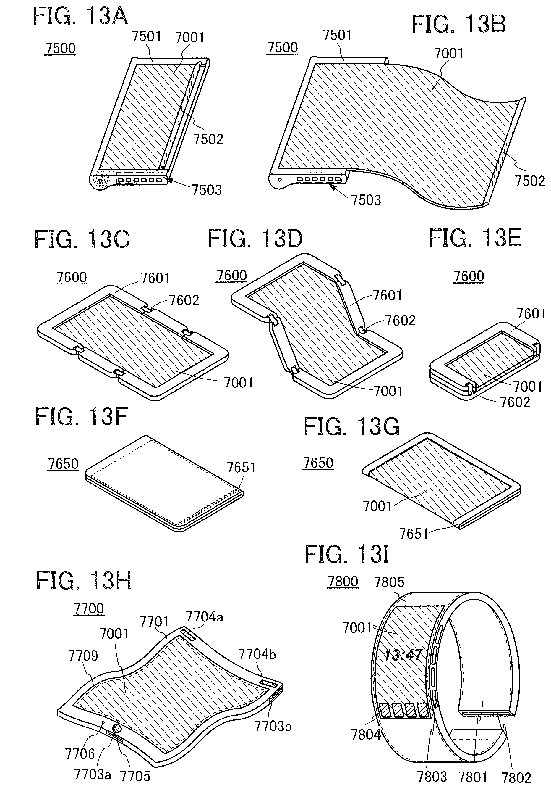
D00014
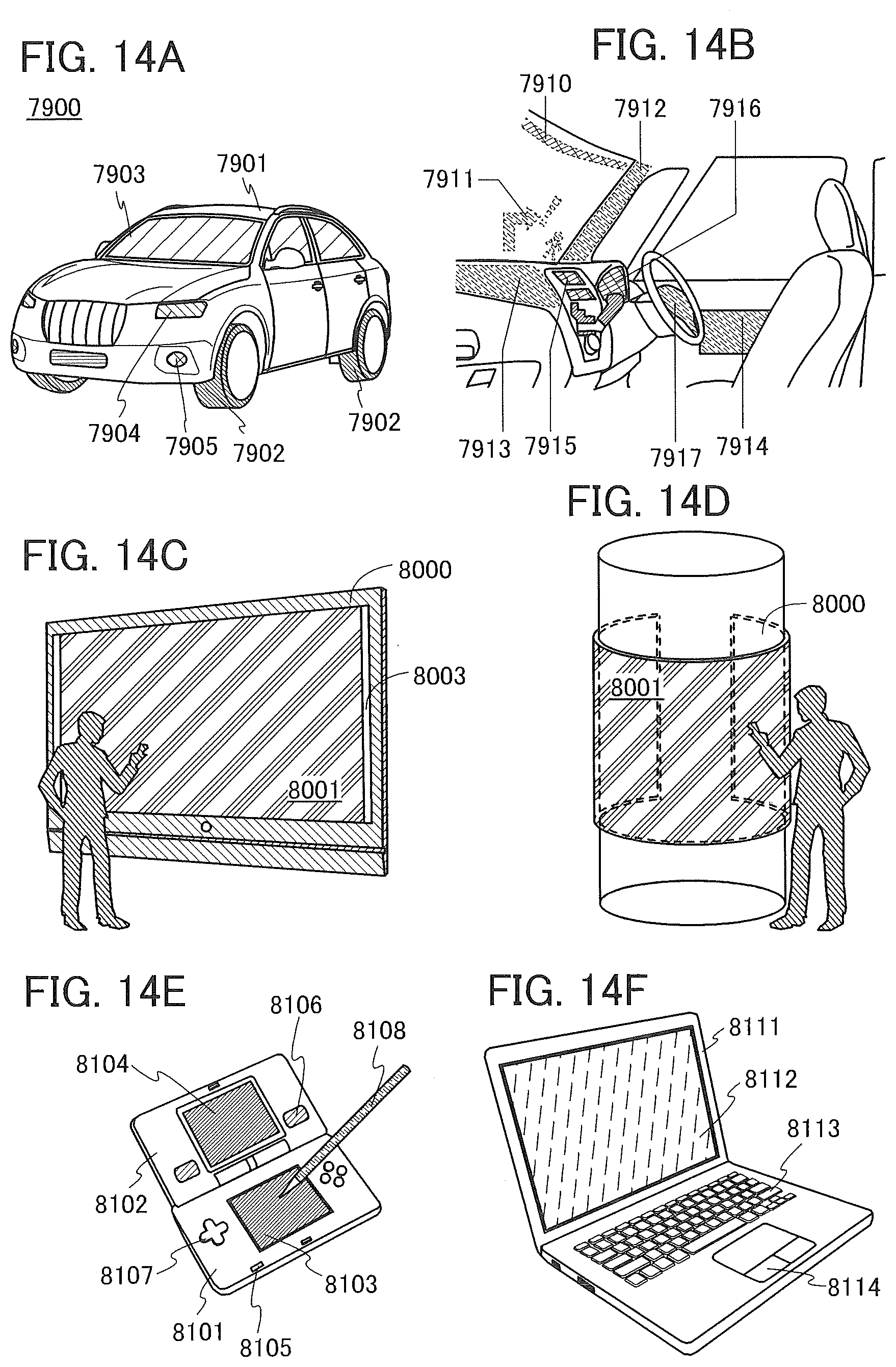
XML
uspto.report is an independent third-party trademark research tool that is not affiliated, endorsed, or sponsored by the United States Patent and Trademark Office (USPTO) or any other governmental organization. The information provided by uspto.report is based on publicly available data at the time of writing and is intended for informational purposes only.
While we strive to provide accurate and up-to-date information, we do not guarantee the accuracy, completeness, reliability, or suitability of the information displayed on this site. The use of this site is at your own risk. Any reliance you place on such information is therefore strictly at your own risk.
All official trademark data, including owner information, should be verified by visiting the official USPTO website at www.uspto.gov. This site is not intended to replace professional legal advice and should not be used as a substitute for consulting with a legal professional who is knowledgeable about trademark law.