Optical Modulating Device, Back Light Module, Display Apparatus, And Fabricating Method Thereof
Qi; Yonglian ; et al.
U.S. patent application number 16/080592 was filed with the patent office on 2020-02-13 for optical modulating device, back light module, display apparatus, and fabricating method thereof. This patent application is currently assigned to BOE Technology Group Co., Ltd.. The applicant listed for this patent is Beijing BOE Display Technology Co., Ltd., BOE Technology Group Co., Ltd.. Invention is credited to Bingqiang Gui, Shuai Liu, Yonglian Qi, Lianjie Qu, Guangdong Shi, Xianxue Yang, Hebin Zhao.
| Application Number | 20200052170 16/080592 |
| Document ID | / |
| Family ID | 65723212 |
| Filed Date | 2020-02-13 |


| United States Patent Application | 20200052170 |
| Kind Code | A1 |
| Qi; Yonglian ; et al. | February 13, 2020 |
OPTICAL MODULATING DEVICE, BACK LIGHT MODULE, DISPLAY APPARATUS, AND FABRICATING METHOD THEREOF
Abstract
The present application provides an optical modulating device having a light transmissive region and a light blocking region. The optical modulating device includes a base substrate; a plurality of protrusions on the base substrate in the light transmissive region and configured to allow light emitting out of a side of the optical modulating device; and a reflective layer on the base substrate in the light blocking region and configured to block light from emitting out of the side of the optical modulating device.
| Inventors: | Qi; Yonglian; (Beijing, CN) ; Qu; Lianjie; (Beijing, CN) ; Zhao; Hebin; (Beijing, CN) ; Gui; Bingqiang; (Beijing, CN) ; Yang; Xianxue; (Beijing, CN) ; Liu; Shuai; (Beijing, CN) ; Shi; Guangdong; (Beijing, CN) | ||||||||||
| Applicant: |
|
||||||||||
|---|---|---|---|---|---|---|---|---|---|---|---|
| Assignee: | BOE Technology Group Co.,
Ltd. Beijing CN Beijing BOE Display Technology Co., Ltd. Beijing CN |
||||||||||
| Family ID: | 65723212 | ||||||||||
| Appl. No.: | 16/080592 | ||||||||||
| Filed: | March 20, 2018 | ||||||||||
| PCT Filed: | March 20, 2018 | ||||||||||
| PCT NO: | PCT/CN2018/079593 | ||||||||||
| 371 Date: | August 28, 2018 |
| Current U.S. Class: | 1/1 |
| Current CPC Class: | H01L 2933/0058 20130101; G02B 6/0055 20130101; G02B 6/0065 20130101; G02F 1/133603 20130101; G02B 5/00 20130101; H01L 33/60 20130101 |
| International Class: | H01L 33/60 20060101 H01L033/60; G02F 1/1335 20060101 G02F001/1335; F21V 8/00 20060101 F21V008/00 |
Foreign Application Data
| Date | Code | Application Number |
|---|---|---|
| Sep 18, 2017 | CN | 201710840999.4 |
Claims
1. An optical modulating device having a light transmissive region and a light blocking region, comprising: a base substrate; a plurality of protrusions on the base substrate in the light transmissive region and configured to allow light emitting out of a side of the optical modulating device; and a reflective layer on the base substrate in the light blocking region and configured to block light from emitting out of the side of the optical modulating device.
2. The optical modulating device of claim 1, wherein each of the plurality of protrusions has a first surface on which the reflective layer is absent and a second surface on which the reflective layer is present; the second surface connecting the first surface with the base substrate; the first surface is in the light transmissive region; and the second surface is in the light blocking region.
3. The optical modulating device of claim 2, wherein an orthographic projection of the plurality of protrusions on the base substrate is at least partially non-overlapping with an orthographic projection of the reflective layer on the base substrate; and an orthographic projection of the first surface of the plurality of protrusions on the base substrate is substantially non-overlapping with the orthographic projection of the reflective layer on the base substrate.
4. The optical modulating device of claim 1, further comprising a plurality of recesses in the light transmissive region, each of which on a side of one of the plurality of protrusions distal to the base substrate; wherein an orthographic projection of the plurality of recesses on the base substrate is substantially non-overlapping with an orthographic projection of the reflective layer on the base substrate.
5. The optical modulating device of claim 4, further comprising an insulating layer on a side of the plurality of protrusions distal to the base substrate; wherein the insulating layer comprises a plurality of insulating blocks, each of which in one of the plurality of recesses and in the light transmissive region.
6. The optical modulating device of claim 1, wherein the base substrate and the plurality of protrusions are formed as an integral light transmission layer.
7. The optical modulating device of claim 1, wherein the plurality of protrusions are a plurality of nanoscale protrusions.
8. The optical modulating device of claim 1, wherein the optical modulating device is a light guide plate.
9. A back light module, comprising the optical modulating device of claim 1 and one or more light sources.
10. A display apparatus, comprising the back light module of claim 9.
11. A method of fabricating an optical modulating device having a light transmissive region and a light blocking region, comprising: forming a light transmission layer comprising a plurality of protrusions on a base substrate in the light transmissive region and configured to allow light emitting out of a side of the plurality of protrusions; and forming a reflective layer on the base substrate in the light blocking region and configured to block light from emitting out of the light transmission layer.
12. The method of claim 11, wherein prior to forming the reflective layer, further comprising forming an insulating layer having a plurality of insulating blocks, each of which on a side of one of the plurality of protrusions distal to the base substrate.
13. The method of claim 12, wherein forming the reflective layer comprises forming a reflective material layer on the base substrate in a region outside the plurality of insulating blocks.
14. The method of claim 12, wherein forming the reflective layer comprises: forming a reflective material layer throughout the light transmission layer, the reflective material layer being formed to cover a region having the plurality of insulating blocks and a region outside the plurality of insulating blocks; and removing the insulating layer; wherein a portion of the reflective material layer on a side of the plurality of insulating blocks distal to the base substrate is removed together with the insulating layer, thereby forming a reflective layer.
15. The method of claim 11, further comprising: forming a mold; embossing a light transmission main body using the mold; and separating the mold from the light transmission main body to form the light transmission layer having the plurality of protrusions on the base substrate.
16. The method of claim 15, wherein forming the mold comprises: forming a replication master layer on a second base substrate, the replication master layer is formed to include a plurality of replication masters corresponding to the plurality of protrusions to be formed in the optical modulating device; forming a conductive surface on an exposed surface of the replication master layer and the second base substrate; forming a metal layer on the conductive surface; and separating the metal layer from the replication master layer and the second base substrate, thereby forming the mold.
17. The method of claim 15, wherein embossing the light transmission main body comprises: embossing the light transmission main body using the mold, thereby forming a light transmission layer having a plurality of protrusions on a base substrate, and a plurality of recesses, each of which on a side of one of the plurality of protrusions distal to the base substrate.
18. The method of claim 17, wherein prior to forming the reflective layer, further comprising forming an insulating layer having a plurality of insulating blocks, each of which on a side of one of the plurality of protrusions distal to the base substrate; wherein forming the insulating layer comprises: printing an ink in the plurality of recesses on a side of the plurality of protrusions distal to the base substrate; and curing the ink in the plurality of recesses on a side of the plurality of protrusions distal to the base substrate, thereby forming the insulating layer having a plurality of insulating blocks, each of which in one of the plurality of recesses.
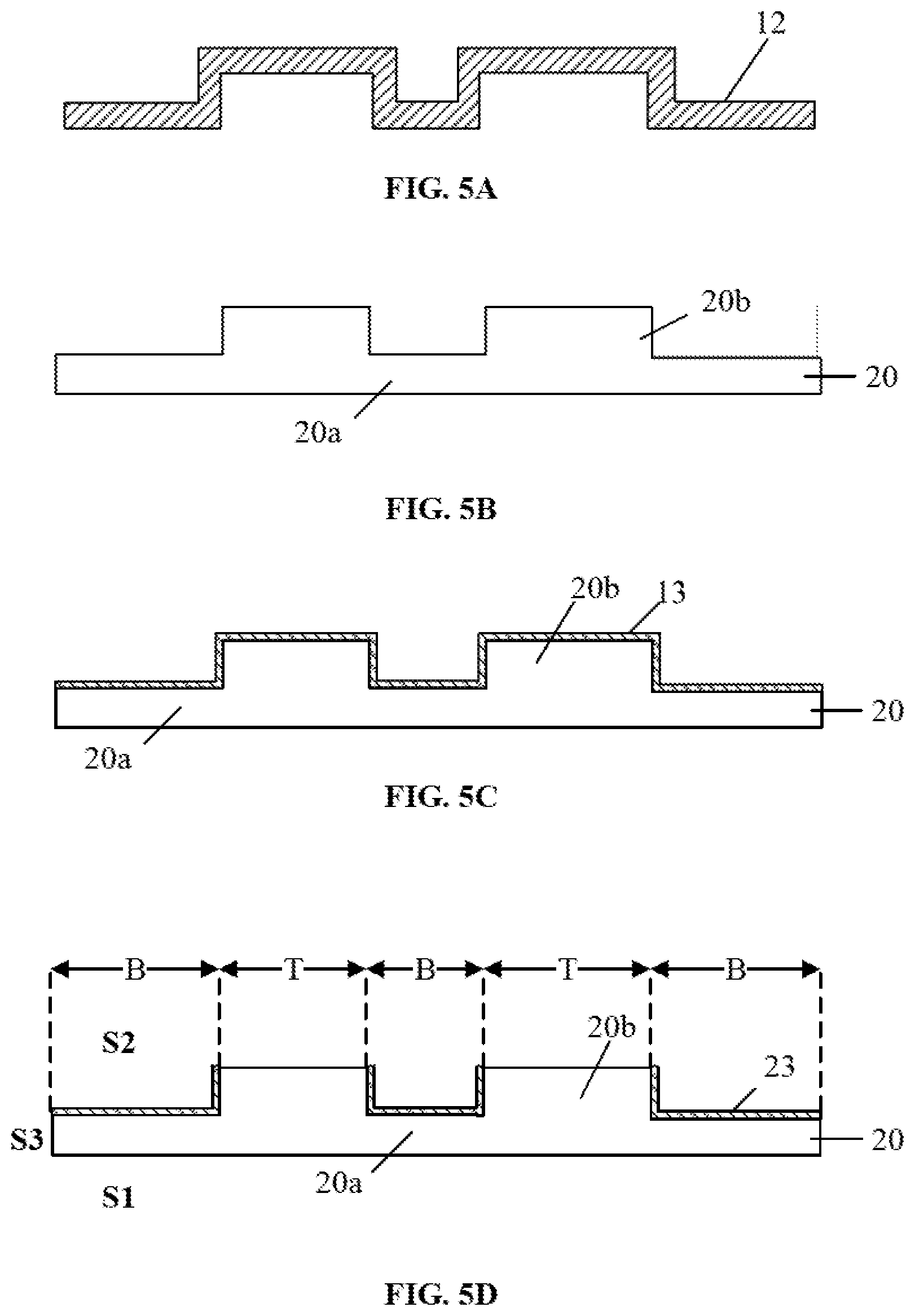
19. The method of claim 11, wherein forming the light transmission layer comprises forming the plurality of protrusions and the base substrate as an integral structure.
20. The method of claim 12, wherein forming the reflective layer comprises: forming a reflective material layer throughout the light transmission layer, the reflective material layer being formed to cover a region having the plurality of protrusions and a region outside the plurality of protrusions; and removing a portion of the reflective material layer on a side of the plurality of insulating blocks distal to the base substrate thereby forming the reflective layer.
Description
CROSS-REFERENCE TO RELATED APPLICATION
[0001] This application claims priority to Chinese Patent Application No. 201710840999.4, filed Sep. 18, 2017, the contents of which are incorporated by reference in the entirety.
TECHNICAL FIELD
[0002] The present invention relates to display technology, more particularly, to a back light module, a display apparatus, and a method of fabricating an optical modulating device.
BACKGROUND
[0003] Typically, a back light module is required in a liquid crystal display apparatus. The back light module includes one or more light sources and a light guide plate for receiving light from the one or more light sources and guiding the light along a transmission direction. The light guide plate enhances the brightness and ensures the light is evenly distributed in a display panel. Typically, a light guide plate includes numerous light guide points (a.k.a., light guide pattern or light guide dots), which disrupt light total reflection locally and reflect light into the display panel along a direction perpendicular to the incident light direction.
SUMMARY
[0004] In one aspect, the present invention provides an optical modulating device having a light transmissive region and a light blocking region, comprising a base substrate; a plurality of protrusions on the base substrate in the light transmissive region and configured to allow light emitting out of a side of the optical modulating device; and a reflective layer on the base substrate in the light blocking region and configured to block light from emitting out of the side of the optical modulating device.
[0005] Optionally, each of the plurality of protrusions has a first surface on which the reflective layer is absent and a second surface on which the reflective layer is present; the second surface connecting the first surface with the base substrate; the first surface is in the light transmissive region; and the second surface is in the light blocking region.
[0006] Optionally, an orthographic projection of the plurality of protrusions on the base substrate is at least partially non-overlapping with an orthographic projection of the reflective layer on the base substrate; and an orthographic projection of the first surface of the plurality of protrusions on the base substrate is substantially non-overlapping with the orthographic projection of the reflective layer on the base substrate.
[0007] Optionally, the optical modulating device further comprises a plurality of recesses in the light transmissive region, each of which on a side of one of the plurality of protrusions distal to the base substrate; wherein an orthographic projection of the plurality of recesses on the base substrate is substantially non-overlapping with an orthographic projection of the reflective layer on the base substrate.
[0008] Optionally, the optical modulating device further comprises an insulating layer on a side of the plurality of protrusions distal to the base substrate; wherein the insulating layer comprises a plurality of insulating blocks, each of which in one of the plurality of recesses and in the light transmissive region.
[0009] Optionally, the base substrate and the plurality of protrusions are formed as an integral light transmission layer.
[0010] Optionally, the plurality of protrusions are a plurality of nanoscale protrusions.
[0011] Optionally, the optical modulating device is a light guide plate.
[0012] In another aspect, the present invention provides a back light module comprising the optical modulating device described herein and one or more light sources.
[0013] In another aspect, the present invention provides a display apparatus comprising the back light module described herein.
[0014] In another aspect, the present invention provides a method of fabricating an optical modulating device having a light transmissive region and a light blocking region, comprising forming a light transmission layer comprising a plurality of protrusions on a base substrate in the light transmissive region and configured to allow light emitting out of a side of the plurality of protrusions; and forming a reflective layer on the base substrate in the light blocking region and configured to block light from emitting out of the light transmission layer.
[0015] Optionally, prior to forming the reflective layer, further comprising forming an insulating layer having a plurality of insulating blocks, each of which on a side of one of the plurality of protrusions distal to the base substrate.
[0016] Optionally, forming the reflective layer comprises forming a reflective material layer on the base substrate in a region outside the plurality of insulating blocks.
[0017] Optionally, forming the reflective layer comprises forming a reflective material layer throughout the light transmission layer, the reflective material layer being formed to cover a region having the plurality of insulating blocks and a region outside the plurality of insulating blocks; and removing the insulating layer; wherein a portion of the reflective material layer on a side of the plurality of insulating blocks distal to the base substrate is removed together with the insulating layer, thereby forming a reflective layer.
[0018] Optionally, the method further comprises forming a mold; embossing a light transmission main body using the mold; and separating the mold from the light transmission main body to form the light transmission layer having the plurality of protrusions on the base substrate.
[0019] Optionally, forming the mold comprises forming a replication master layer on a second base substrate, the replication master layer is formed to include a plurality of replication masters corresponding to the plurality of protrusions to be formed in the optical modulating device; forming a conductive surface on an exposed surface of the replication master layer and the second base substrate; forming a metal layer on the conductive surface; and separating the metal layer from the replication master layer and the second base substrate, thereby forming the mold.
[0020] Optionally, embossing the light transmission main body comprises embossing the light transmission main body using the mold, thereby forming a light transmission layer having a plurality of protrusions on a base substrate, and a plurality of recesses, each of which on a side of one of the plurality of protrusions distal to the base substrate.
[0021] Optionally, prior to forming the reflective layer, further comprising forming an insulating layer having a plurality of insulating blocks, each of which on a side of one of the plurality of protrusions distal to the base substrate; wherein forming the insulating layer comprises printing an ink in the plurality of recesses on a side of the plurality of protrusions distal to the base substrate; and curing the ink in the plurality of recesses on a side of the plurality of protrusions distal to the base substrate, thereby forming the insulating layer having a plurality of insulating blocks, each of which in one of the plurality of recesses.
[0022] Optionally, forming the light transmission layer comprises forming the plurality of protrusions and the base substrate as an integral structure.
[0023] Optionally, forming the reflective layer comprises forming a reflective material layer throughout the light transmission layer, the reflective material layer being formed to cover a region having the plurality of protrusions and a region outside the plurality of protrusions; and removing a portion of the reflective material layer on a side of the plurality of insulating blocks distal to the base substrate thereby forming the reflective layer.
BRIEF DESCRIPTION OF THE FIGURES
[0024] The following drawings are merely examples for illustrative purposes according to various disclosed embodiments and are not intended to limit the scope of the present invention.
[0025] FIG. 1A is a schematic diagram illustrating the structure of an optical modulating device in some embodiments according to the present disclosure.
[0026] FIG. 1B is a plan view of the optical modulating device in FIG. 1A.
[0027] FIG. 2 is a zoom-in view of one of the plurality of protrusions in an optical modulating device in some embodiments according to the present disclosure.
[0028] FIG. 3 is a schematic diagram illustrating the structure of an optical modulating device in some embodiments according to the present disclosure.
[0029] FIG. 4 is a schematic diagram illustrating the structure of an optical modulating device in some embodiments according to the present disclosure.
[0030] FIGS. 5A to 5D illustrate a process of fabricating an optical modulating device in some embodiments according to the present disclosure.
[0031] FIG. 6 is a flow chart illustrating a process of fabricating an optical modulating device in some embodiments according to the present disclosure.
[0032] FIG. 7 is a flow chart illustrating a process of fabricating an optical modulating device in some embodiments according to the present disclosure.
[0033] FIGS. 8A to 8H illustrate a process of fabricating an optical modulating device in some embodiments according to the present disclosure.
[0034] FIG. 9 is a flow chart illustrating a process of fabricating an optical modulating device in some embodiments according to the present disclosure.
[0035] FIGS. 10A to 10B illustrate a process of fabricating an optical modulating device in some embodiments according to the present disclosure.
DETAILED DESCRIPTION
[0036] The disclosure will now be described more specifically with reference to the following embodiments. It is to be noted that the following descriptions of some embodiments are presented herein for purpose of illustration and description only. It is not intended to be exhaustive or to be limited to the precise form disclosed.
[0037] The present disclosure provides, inter alia, an optical modulating device, a back light module, a display apparatus, and a method of fabricating an optical modulating device that substantially obviate one or more of the problems due to limitations and disadvantages of the related art. In one aspect, the present disclosure provides an optical modulating device having a light transmissive region and a light blocking region. In some embodiments, the optical modulating device includes a base substrate; a plurality of protrusions on the base substrate in the light transmissive region and configured to allow light emitting out of a side of the optical modulating device; and a reflective layer on the base substrate in the light blocking region and configured to block light from emitting out of the side of the optical modulating device.
[0038] FIG. 1A is a schematic diagram illustrating the structure of an optical modulating device in some embodiments according to the present disclosure. FIG. 1B is a plan view of the optical modulating device in FIG. 1A. Referring to FIG. 1A and FIG. 1B, the optical modulating device 100 in some embodiments has a first side S1 (e.g., a bottom side), a second side S2 (e.g., a top side) substantially opposite to the first side S1, and a third side S3 (e.g., a lateral side) connecting the first side S1 and the second side S2. In some embodiments, the second side S2 is a light emitting side of the optical modulating device 100, e.g., light emits out of the optical modulating device 100 from the second side S2. The optical modulating device 100 in some embodiments has a light transmissive region T and a light blocking region B. Light emits out of the optical modulating device 100 from the light transmissive region T on the second side S2, and light is substantially blocked in the light blocking region B on the second side S2. Optionally, at least a portion of the first side S1 is substantially light transmissive, and light from one or more light sources enters the optical modulating device 100 from the first side S1 (direct-lit type). Optionally, at least a portion of the third side S3 is substantially light transmissive, and light from one or more light sources enters the optical modulating device 100 from the third side S3 (edge-lit type).
[0039] In some embodiments, the optical modulating device 100 includes a base substrate 20a, a plurality of protrusions 20b on the base substrate 20a in the light transmissive region T and configured to allow light emitting out of the second side S2, and a reflective layer 23 on the base substrate 20a in the light blocking region B and configured to block light from emitting out of the second side S2. Optionally, the base substrate 20a and the plurality of protrusions 20b constitute an integral structure. Optionally, the base substrate 20a and the plurality of protrusions 20b are made of a substantially transparent material. As used herein, the term "substantially transparent" means at least 50 percent (e.g., at least 60 percent, at least 70 percent, at least 80 percent, at least 90 percent, and at least 95 percent) of light in the visible wavelength range transmitted therethrough. Optionally, the plurality of protrusions 20b are spaced apart from each other by the reflective layer 23. As shown in FIG. 1A and FIG. 1B, in some embodiments, the reflective layer 23 corresponds to the light blocking region B, and the plurality of protrusions 20b correspond to the light transmissive region T.
[0040] Optionally, the plurality of protrusions 20b are a plurality of nanoscale protrusions. As used herein, the term "nanoscale" refers to structures having sizes or dimensions (e.g., diameters) no greater than 1000 nanometers (nm), e.g., in a range of approximately 10 nm to approximately 1000 nm, approximately 10 nm to approximately 100 nm, approximately 100 nm to approximately 200 an, approximately 200 urn to approximately 300 an, approximately 300 nm to approximately 400 nm, approximately 400 nm to approximately 500 nm, approximately 500 nm to approximately 600 nm, approximately 600 nm to approximately 700 nm, approximately 700 nm to approximately 800 nm, approximately 800 n to approximately 900 nm, approximately 900 nm to approximately 1000 nm.
[0041] FIG. 2 is a zoom-in view of one of the plurality of protrusions in an optical modulating device in some embodiments according to the present disclosure. Referring to FIG. 2, each of the plurality of protrusions 20b in some embodiments has an exposed surface Se on which the reflective layer 23 is absent, and a covered surface Sc on which the reflective layer 23 is present. Optionally, the covered surface Sc is a lateral surface of each of the plurality of protrusions 20b, the covered surface Sc connecting the exposed surface Se with the base substrate 20a. The exposed surface Se is in the light transmissive region T, and the covered surface Sc is in the light blocking region B. By having the reflective layer 23 at least partially covers the lateral surface of the plurality of protrusions 20b, the light emitted from the optical modulating device can be further aligned.
[0042] In some embodiments, an orthographic projection of the plurality of protrusions 20b on the base substrate 20a is at least partially non-overlapping with an orthographic projection of the reflective layer 23 on the base substrate 20a. Optionally, the orthographic projection of the plurality of protrusions 20b on the base substrate 20a is substantially non-overlapping with the orthographic projection of the reflective layer 23 on the base substrate 20a. Optionally, an orthographic projection of the exposed surface Se of the plurality of protrusions 20b on the base substrate 20a is substantially non-overlapping with the orthographic projection of the reflective layer 23 on the base substrate 20a.
[0043] Various appropriate shapes may be adopted for the plurality of protrusions 20b. Examples of appropriate shapes for the plurality of protrusions 20b include a cylinder, a truncated cylinder, a domed cylinder, a sphere, a hemisphere, a sub-hemisphere, a cube, a cuboid, a pyramid, a cone, a truncated cone, a triangular prism, a barrel, and so on.
[0044] Various appropriate reflective materials and various appropriate fabricating methods may be used for making the reflective layer 23. Examples of appropriate reflective materials for making the reflective layer 23 include metals having high reflectivity such as silver and aluminum.
[0045] Optionally, the optical modulating device 100 is a light guide plate. Optionally, the second side S2 of the optical modulating device 100 is a light emitting side of the optical modulating device 100 for providing a back light for a display panel. Optionally, one or more light sources may be disposed on the first side S1 or on the third side S3, or both.
[0046] In some embodiments, and as shown in FIG. 1A and FIG. 2, the plurality of protrusions 20b have a substantially leveled surface.
[0047] FIG. 3 is a schematic diagram illustrating the structure of an optical modulating device in some embodiments according to the present disclosure. Referring to FIG. 3, the optical modulating device 100 in some embodiments further includes a plurality of recesses R in the light transmissive region T, each of which on a side of one of the plurality of protrusions 20b distal to the base substrate 20a. An orthographic projection of the plurality of recesses R on the base substrate 20a is at least partially non-overlapping with an orthographic projection of the reflective layer 23 on the base substrate 20a. Optionally, the orthographic projection of the plurality of recesses R on the base substrate 20a is substantially non-overlapping with the orthographic projection of the reflective layer 23 on the base substrate 20a. Optionally, an orthographic projection of the exposed surface Se of the plurality of protrusions 20b on the base substrate 20a substantially overlaps with the orthographic projection of the plurality of recesses R on the base substrate 20a.
[0048] Optionally, the plurality of recesses R are a plurality of nanoscale recesses. Optionally, the plurality of recesses R have sizes or dimensions (e.g., diameters) no greater than 1000 nanometers (urn), e.g., in a range of approximately 10 nm to approximately 1000 nm, approximately 10 nm to approximately 100 nm, approximately 100 nm to approximately 200 nm, approximately 200 nm to approximately 300 nm, approximately 300 urn to approximately 400 nm, approximately 400 nm to approximately 500 nm, approximately 500 nm to approximately 600 an, approximately 600 urn to approximately 700 nm, approximately 700 urn to approximately 800 nm, approximately 800 n to approximately 900 nm, approximately 900 nm to approximately 1000 nm.
[0049] FIG. 4 is a schematic diagram illustrating the structure of an optical modulating device in some embodiments according to the present disclosure. Referring to FIG. 4, the optical modulating device 100 in some embodiments further includes an insulating layer 22 on a side of the plurality of protrusions 20b distal to the base substrate 20a. The insulating layer 22 includes a plurality of insulating blocks 22b, each of which in one of the plurality of recesses R and in the light transmissive region T. Optionally, the insulating layer 22 is made of a substantially transparent material. Optionally, an orthographic projection of the plurality of insulating blocks 22b on the base substrate 20a is at least partially non-overlapping with an orthographic projection of the reflective layer 23 on the base substrate 20a. Optionally, the orthographic projection of the plurality of insulating blocks 22b on the base substrate 20a is substantially non-overlapping with the orthographic projection of the reflective layer 23 on the base substrate 20a. Optionally, an orthographic projection of the exposed surface Se of the plurality of protrusions 20b on the base substrate 20a substantially overlaps with the orthographic projection of the plurality of insulating blocks 22b on the base substrate 20a.
[0050] Optionally, the plurality of insulating blocks 22b are a plurality of nanoscale insulating blocks. Optionally, the plurality of insulating blocks 22b have sizes or dimensions (e.g., diameters) no greater than 1000 nanometers (nm), e.g., in a range of approximately 10 nm to approximately 1000 nm, approximately 10 nm to approximately 100 nm, approximately 100 nm to approximately 200 in, approximately 200 m to approximately 300 nm, approximately 300 nm to approximately 400 in, approximately 400 nm to approximately 500 nm, approximately 500 nm to approximately 600 nm, approximately 600 nm to approximately 700 n, approximately 700 nm to approximately 800 nm, approximately 800 nm to approximately 900 nm, approximately 900 m to approximately 1000 nm.
[0051] In another aspect, the present disclosure provides a method of fabricating an optical modulating device having a light transmissive region and a light blocking region. The optical modulating device is fabricated to have a first side (e.g., a bottom side), a second side (e.g., a top side) substantially opposite to the first side, and a third side (e.g., a lateral side) connecting the first side and the second side. In some embodiments, the second side is a light emitting side of the optical modulating device, e.g., light emits out of the optical modulating device from the second side. Light emits out of the optical modulating device from the light transmissive region on the second side, and light is substantially blocked in the light blocking region on the second side.
[0052] In some embodiments, the method includes forming a light transmission layer having a plurality of protrusions in the light transmissive region and configured to allow light emitting out of the plurality of protrusions, and forming a reflective layer on the base substrate in the light blocking region and configured to block light from emitting out of the light transmission layer. Optionally, the base substrate and the plurality of protrusions are formed as an integral structure. Optionally, the base substrate and the plurality of protrusions are made of a substantially transparent material. Optionally, the plurality of protrusions are formed to be spaced apart from each other by the reflective layer. Optionally, the reflective layer is formed in the light blocking region, and the plurality of protrusions are formed in the light transmissive region.
[0053] FIGS. 5A to 5D illustrate a process of fabricating an optical modulating device in some embodiments according to the present disclosure. Referring to FIG. 5A to FIG. 5D, the method in some embodiments includes forming a mold 12 (FIG. 5A), embossing a light transmission main body using the mold 12 and separating the mold 12 from the light transmission main body to form a light transmission layer 20 having a plurality of protrusions 20b on a base substrate 20a (FIG. 5B), forming a reflective material layer 13 on the light transmission layer 20 having the plurality of protrusions 20b and the base substrate 20a (FIG. 5C), and removing a portion of the reflective material layer 13 on the plurality of protrusions 20b to form a reflective layer 23 (FIG. 5D). The reflective layer 23 is formed in the light blocking region B and configured to block light from emitting out of the second side S2.
[0054] FIG. 6 is a flow chart illustrating a process of fabricating an optical modulating device in some embodiments according to the present disclosure. Referring to FIG. 6, the method in some embodiments includes forming a light transmission layer having a base substrate and a plurality of protrusions on the base substrate, the plurality of protrusions being a plurality of nanoscale protrusions spaced apart from each other and being light transmissive; forming an insulating layer having a plurality of insulating blocks, each of which on a side of one of the plurality of protrusions distal to the base substrate; and forming a reflective layer on the base substrate in a region outside the plurality of insulating blocks. Optionally, the reflective layer is made of a metallic material.
[0055] By first forming an insulating layer covering a top surface of the plurality of protrusions, the reflective layer can be formed only in a region outside the top surface of the plurality of protrusions. In one example, by first forming the insulating layer covering the top surface of the plurality of protrusions, the reflective material is not deposited on the top surface of the plurality of protrusions at all. For example, the surface of the light transmission layer can be treated to become conductive prior to forming the insulating layer, followed by forming the plurality of insulating blocks on top of the plurality of protrusions. Subsequently, the reflective material is deposited on the conductive surface by, e.g., electrodeposition. Because the top surface of the plurality of protrusions are covered by the plurality of insulating blocks which is not conductive, the reflective material is not deposited on the plurality of insulating blocks. In another example, the insulating layer is first formed to cover the top surface of the plurality of protrusions, a reflective material layer is then formed throughout the surface of the light transmission layer, the plurality of insulating blocked is then removed subsequent to forming the reflective material layer. A portion of the reflective material layer on top of the plurality of insulating blocks is also removed during the process of removing the plurality of insulating blocks, thereby forming the reflective layer. The reflective layer so formed does not cover the top surface of the plurality of protrusions.
[0056] Optionally, each of the plurality of protrusions is formed to have an exposed on which the reflective layer is absent, and a covered surface on which the reflective layer 23 is present. Optionally, the exposed surface is a top surface of each of the plurality of protrusions. Optionally, the covered surface is a lateral surface of each of the plurality of protrusions, the covered surface connecting the exposed surface with the base substrate. The exposed surface is formed in the light transmissive region, and the covered surface is formed in the light blocking region. By having the reflective layer at least partially covers the lateral surface of the plurality of protrusions, the light emitted from the optical modulating device can be further aligned.
[0057] The plurality of protrusions may be formed to have various appropriate shapes. Examples of appropriate shapes for the plurality of protrusions include a cylinder, a truncated cylinder, a domed cylinder, a sphere, a hemisphere, a sub-hemisphere, a cube, a cuboid, a pyramid, a cone, a truncated cone, a triangular prism, a barrel, and so on.
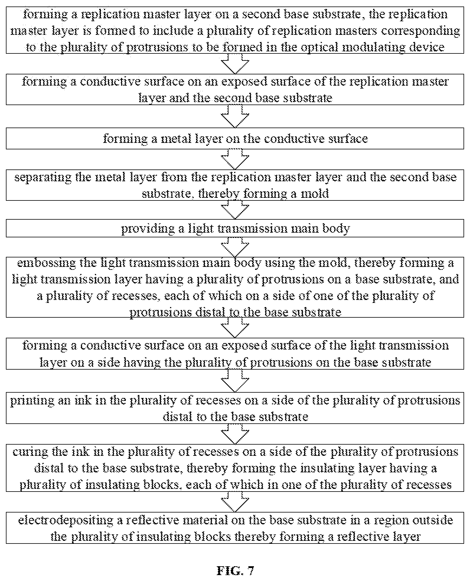
[0058] FIG. 7 is a flow chart illustrating a process of fabricating an optical modulating device in some embodiments according to the present disclosure. FIGS. 8A to 8H illustrate a process of fabricating an optical modulating device in some embodiments according to the present disclosure. Referring to FIG. 8E, the method in some embodiments includes forming a light transmission layer 20 having a base substrate 20a and a plurality of protrusions 20b on the base substrate 20a. The plurality of protrusions 20b are formed as a plurality of nanoscale protrusions spaced apart from each other and are light transmissive. As shown in FIG. 8E, the light transmission layer 20 is formed to have a plurality of recesses R respectively, each of which on a side of one of the plurality of protrusions 20b distal to the base substrate 20a. The plurality of recesses R may be formed to have various appropriate shapes configured to contain a liquid. Optionally, the optical modulating device is made of a polymer material. Optionally, the light transmission layer 20 is formed using an embossing process.
[0059] Referring to FIG. 8C, the method in some embodiments includes forming a mold 33. Referring to FIG. 7, the step of forming the mold in some embodiments includes forming a replication master layer 32 on a second base substrate 31, the replication master layer 32 is formed to include a plurality of replication masters 32a corresponding to the plurality of protrusions to be formed in the optical modulating device. Optionally, the plurality of replication masters 32a are equivalent to the plurality of protrusions in terms of size, dimension, and shape. Optionally, a photoresist layer is first formed on the second base substrate 31, followed by exposure and development, thereby forming the replication master layer 32. Referring to FIG. 7, the step of forming the mold in some embodiments further includes forming a conductive surface on an exposed surface of the replication master layer 32 and the second base substrate 31. For example, the conductive surface is formed on the top surface and the lateral surface of each of the plurality of replication masters 32a, and is formed on the second base substrate 31 in a region not covered by the plurality of replication masters 32a. Referring to FIG. 7, the step of forming the mold in some embodiments further includes forming a metal layer 331 on the conductive surface (see, e.g., FIG. 8B). Optionally, the metal layer 331 includes nickel. Referring to FIG. 7, the step of forming the mold in some embodiments further includes separating the metal layer 331 from the replication master layer 32 and the second base substrate 31, thereby forming a mold 33 (see, e.g., FIG. 8C).
[0060] Referring to FIG. 7, the method in some embodiments further includes providing a light transmission main body 34. Optionally, the light transmission main body 34 is made of a polymer material.
[0061] Referring to FIG. 7, the method in some embodiments further includes embossing the light transmission main body 34 using the mold 33, thereby forming a light transmission layer 20 having a plurality of protrusions 20b on a base substrate 20a, and a plurality of recesses R, each of which on a side of one of the plurality of protrusions 20b distal to the base substrate 20a (see, e.g., FIG. 8D and FIG. 8E).
[0062] Referring to FIG. 7, the method in some embodiments further includes forming a conductive surface on an exposed surface of the light transmission layer 20 on a side having the plurality of protrusions 20b on the base substrate 20a. Referring to FIG. 8E, the light transmission layer 20 in some embodiments has a first side S1 (e.g., a bottom side), a second side S2 (e.g., a top side) substantially opposite to the first side S1, and a third side S3 (e.g., a lateral side) connecting the first side S and the second side S2. The plurality of protrusions 20b are formed on the second side S2 of the light transmission layer 20. Optionally, the conductive surface is formed on the exposed surface of the second side S2 of the light transmission layer 20.
[0063] In some embodiments, the method further includes forming an insulating layer 22 on a side of the plurality of protrusions 20b distal to the base substrate 20a. The insulating layer 22 is formed to include a plurality of insulating blocks 22b, each of which on a side of one of the plurality of protrusions 20b distal to the base substrate 20a (see. e.g., FIG. 8G). Referring to FIG. 7, the step of forming the insulating layer 22 in some embodiments includes printing an ink 221 in the plurality of recesses R on a side of the plurality of protrusions 20b distal to the base substrate 20a (see, e.g., FIG. 8F).
[0064] Referring to FIG. 7, the step of forming the insulating layer 22 in some embodiments further includes curing the ink 221 in the plurality of recesses R on a side of the plurality of protrusions 20b distal to the base substrate 20a, thereby forming the insulating layer 22 having a plurality of insulating blocks 22b, each of which in one of the plurality of recesses R (see, e.g., FIG. 8G).
[0065] In some embodiments, the method further includes forming a reflective layer 23 on the base substrate 20a in a region outside the plurality of insulating blocks 22b. For example, the reflective layer 23 is formed on the base substrate 20a in a region not covered by the plurality of protrusions 20b and on a lateral surface of the plurality of protrusions 20b. Referring to FIG. 7, the step of forming the reflective layer 23 in some embodiments includes electrodepositing a reflective material on the base substrate 20a in a region outside the plurality of insulating blocks 22b thereby forming a reflective layer 23 (see. e.g., FIG. 811H). Because the surface of the light transmission layer 20 is treated to become conductive prior to forming the insulating layer 22, and the insulating layer 22 covers the top surface of the plurality of protrusions 20b, the step of electrodepositing the reflective material would not deposit the reflective material in the region having the insulating layer 22, i.e., the step of electrodepositing the reflective material would only deposit the reflective material on the base substrate 20a in a region not covered by the plurality of protrusions 20b and on a lateral surface of the plurality of protrusions 20b. Optionally, the step of electrodepositing the reflective material is performed by an electroforming process.
[0066] In some embodiments, the method further includes removing the insulating layer 22, e.g., by ashing.
[0067] In some embodiments, the insulating layer 22 is made of a substantially transparent material. Optionally, the insulating layer 22 is not removed, and remains in the optical modulating device.
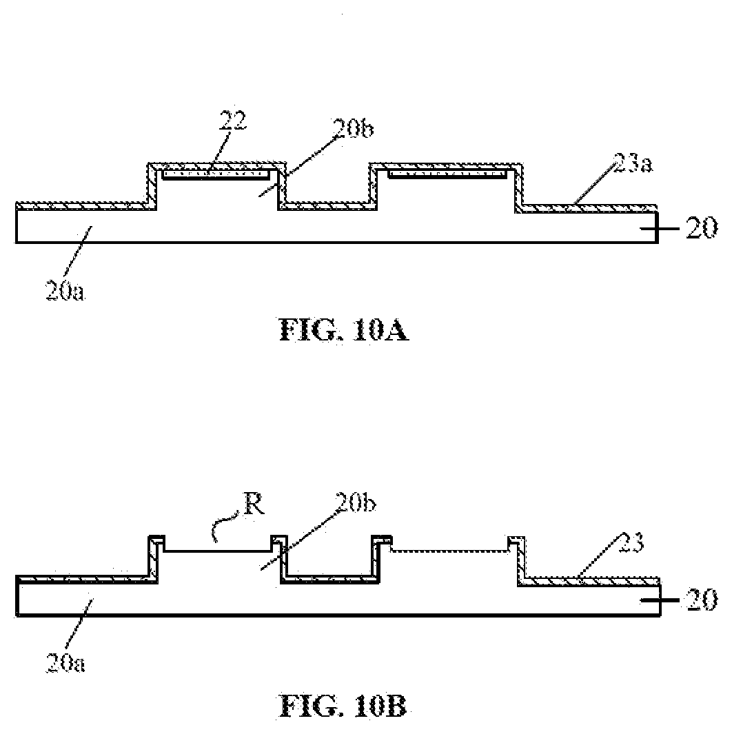
[0068] FIG. 9 is a flow chart illustrating a process of fabricating an optical modulating device in some embodiments according to the present disclosure. FIGS. 10A to 10B illustrate a process of fabricating an optical modulating device in some embodiments according to the present disclosure. Referring to FIG. 9, FIGS. 8A to 8G, and FIGS. 10A to 10B, the method in some embodiments includes forming a mold 33. Referring to FIG. 9 and FIGS. 8A to 8G, the step of forming the mold in some embodiments includes forming a replication master layer 32 on a second base substrate 31, the replication master layer 32 is formed to include a plurality of replication masters 32a corresponding to the plurality of protrusions to be formed in the optical modulating device; forming a conductive surface on an exposed surface of the replication master layer 32 and the second base substrate 31; and forming a metal layer 331 on the conductive surface.
[0069] Referring to FIG. 9 and FIGS. 8A to 8G, the method in some embodiments further includes providing a light transmission main body 34; embossing the light transmission main body 34 using the mold 33, thereby forming a light transmission layer 20 having a plurality of protrusions 20b on a base substrate 20a, and a plurality of recesses R, each of which on a side of one of the plurality of protrusions 20b distal to the base substrate 20a; forming a conductive surface on an exposed surface of the light transmission layer 20 on a side having the plurality of protrusions 20b on the base substrate 20a; and forming an insulating layer 22 on a side of the plurality of protrusions 20b distal to the base substrate 20a. The insulating layer 22 is formed to include a plurality of insulating blocks 22b, each of which on a side of one of the plurality of protrusions 20b distal to the base substrate 20a. Referring to FIG. 9 and FIGS. 8A to 8G, the the step of forming the insulating layer 22 in some embodiments includes printing an ink 221 in the plurality of recesses R on a side of the plurality of protrusions 20b distal to the base substrate 20a; and curing the ink 221 in the plurality of recesses R on a side of the plurality of protrusions 20b distal to the base substrate 20a, thereby forming the insulating layer 22 having a plurality of insulating blocks 22b, each of which in one of the plurality of recesses R.
[0070] Referring to FIG. 9 and FIG. 10A, the method in some embodiments further includes forming a reflective material layer 23a throughout the light transmission layer 20, the reflective material layer 23a being formed to cover a region having the plurality of insulating blocks 22b and a region outside the plurality of insulating blocks 22b. Optionally, the reflective material layer 23a is forming by sputtering a reflective material on the light transmission layer 20.
the plurality of insulating blocked is then removed subsequent to forming the reflective material layer. A portion of the reflective material layer on top of the plurality of insulating blocks is also removed during the process of removing the plurality of insulating blocks, thereby forming the reflective layer. The reflective layer so formed does not cover the top surface of the plurality of protrusions
[0071] Referring to FIG. 9 and FIG. 10B, the method in some embodiments further includes removing the insulating layer 22, a portion of the reflective material layer 23a on a side of the plurality of insulating blocks 22b distal to the base substrate 20a being removed together with the insulating layer 22, thereby forming a reflective layer 23. Optionally, the step of removing the insulating layer is performed by photodecomposition. Optionally, the step of removing the insulating layer is performed by a lift-off process using a solvent.
[0072] In another aspect, the present disclosure provides a back light module having the optical modulating device described herein or fabricated by a method described herein. Optionally, the optical modulating device is a light guide plate in the back light module. The present optical modulating device significantly improves the alignment of light emitted from the back light module. As a result, light utilization rate of the back light module can be substantially enhanced by having the present optical modulating device.
[0073] In another aspect, the present disclosure provides a display apparatus having the back light module described herein. Examples of appropriate touch control display apparatuses include, but are not limited to, an electronic paper, a mobile phone, a tablet computer, a television, a monitor, a notebook computer, a digital album, a GPS, etc.
[0074] The foregoing description of the embodiments of the invention has been presented for purposes of illustration and description. It is not intended to be exhaustive or to limit the invention to the precise form or to exemplary embodiments disclosed. Accordingly, the foregoing description should be regarded as illustrative rather than restrictive. Obviously, many modifications and variations will be apparent to practitioners skilled in this art. The embodiments are chosen and described in order to explain the principles of the invention and its best mode practical application, thereby to enable persons skilled in the art to understand the invention for various embodiments and with various modifications as are suited to the particular use or implementation contemplated. It is intended that the scope of the invention be defined by the claims appended hereto and their equivalents in which all terms are meant in their broadest reasonable sense unless otherwise indicated. Therefore, the term "the invention". "the present invention" or the like does not necessarily limit the claim scope to a specific embodiment, and the reference to exemplary embodiments of the invention does not imply a limitation on the invention, and no such limitation is to be inferred. The invention is limited only by the spirit and scope of the appended claims. Moreover, these claims may refer to use "first", "second", etc. following with noun or element. Such terms should be understood as a nomenclature and should not be construed as giving the limitation on the number of the elements modified by such nomenclature unless specific number has been given. Any advantages and benefits described may not apply to all embodiments of the invention. It should be appreciated that variations may be made in the embodiments described by persons skilled in the art without departing from the scope of the present invention as defined by the following claims. Moreover, no element and component in the present disclosure is intended to be dedicated to the public regardless of whether the element or component is explicitly recited in the following claims.
* * * * *
D00000
D00001
D00002
D00003
D00004
D00005
D00006
D00007
D00008
D00009
XML
uspto.report is an independent third-party trademark research tool that is not affiliated, endorsed, or sponsored by the United States Patent and Trademark Office (USPTO) or any other governmental organization. The information provided by uspto.report is based on publicly available data at the time of writing and is intended for informational purposes only.
While we strive to provide accurate and up-to-date information, we do not guarantee the accuracy, completeness, reliability, or suitability of the information displayed on this site. The use of this site is at your own risk. Any reliance you place on such information is therefore strictly at your own risk.
All official trademark data, including owner information, should be verified by visiting the official USPTO website at www.uspto.gov. This site is not intended to replace professional legal advice and should not be used as a substitute for consulting with a legal professional who is knowledgeable about trademark law.